Comparison of Test Methods for Human Body Model (HBM ...
6
1 Special Edition: Comparison of Test Methods for Human Body Model (HBM) Electrostatic Discharge (ESD) Volume 11, Issue 2, September 27, 2020 Damage from ESD is a cause of major costs to the microcircuit industry in terms of time, money, and mission risk. The EEE Parts Bulletin has released four special issues on ESD [1]–[4]. The first issue, in 2016, stressed the need to upgrade specifications related to ESD and suggested improved ESD practices wherever parts are manufactured, stored, or prepared for shipment. The second ESD special issue, in 2017, focused on a parts failure investigation that ultimately identified ESD as the most likely cause of the failure. The 2017 special issue also included an important reminder about regular ESD testing. The third issue, in 2018, provided an example demonstrating the importance of maintaining ESD discipline and high-level risk analysis related to ESD. The fourth issue, later in 2018, was a compendium of the previous three special issues and included an overall updated view of the subject matter. The current special issue focuses on one specific aspect of ESD damage that is caused by the human body during parts handling. The susceptibility of electronic devices to such damage is characterized by the human body model (HBM). For illustration, the magnitude of electrostatic voltage built up on a chip under different handling means and relative humidity (RH) conditions is shown in Table 1 [1]. A microcircuit device exposed to an ESD event induced by contact with a human body can easily experience an electrostatic voltage attack in the kilovolt range. Thus, a better understanding of HBM ESD events is warranted. In this issue of the EEE Parts Bulletin, we report on independent experimental evaluations of two popular HBM-specific test methods: MIL-STD-883 Test Method 3015.7 [5] and JEDEC JS001-2017 [6]. Similar to the latter, the Automotive Electronics Council (AEC) HBM test method is also included for reference. For a fair and straightforward comparison, a chosen microcircuit chip was subjected to HBM zaps under MIL-STD-883 and JEDEC/AEC conditions, respectively. Table 1. Voltages experienced by electronic devices exposed to various HBM-ESD events [1]. Means of Static Generation Electrostatic Voltages 10–20% RH 65–90% RH Walking across carpet 35,000 1,500 Walking over vinyl floor 12,000 250 Worker at bench 6,000 100 Vinyl envelopes for work instructions 7,000 600 Common poly bag picked up from bench 20,000 1,200 Work chair padded with polyurethane foam 18,000 1,500 HBM Test Standards A good overview of HBM test standards was presented in the first EEE Parts Bulletin special issue on ESD [1]. In this special issue, we compare and evaluate three popular HBM test standards: 1. MIL-STD-883 Test Method 3015.7 (abbreviated MIL- STD-883) [5] 2. JEDEC JS001-2017 (based on JESD22-A114, abbreviated JEDEC-JS001) [6], [7] 3. AEC-Q200-002 REV-B (abbreviated AEC-Q200) [8] In the following sections, test methods and classifications for these three test standards are extracted from their respective specification documents. The test methods and classifications are summarized and compared in Table 5. There are many similarities between JEDEC-JS001 and AEC-Q200, so the primary focus of the comparison was between MIL-STD-883 and JEDEC-JS001.
Transcript of Comparison of Test Methods for Human Body Model (HBM ...

1
Special Edition: Comparison of Test Methods for Human Body Model (HBM) Electrostatic Discharge (ESD)
Volume 11, Issue 2, September 27, 2020
Damage from ESD is a cause of major costs to the microcircuit industry in terms of time, money, and mission risk. The
EEE Parts Bulletin has released four special issues on ESD [1]–[4]. The first issue, in 2016, stressed the need to upgrade
specifications related to ESD and suggested improved ESD practices wherever parts are manufactured, stored, or
prepared for shipment. The second ESD special issue, in 2017, focused on a parts failure investigation that ultimately
identified ESD as the most likely cause of the failure. The 2017 special issue also included an important reminder about
regular ESD testing. The third issue, in 2018, provided an example demonstrating the importance of maintaining ESD
discipline and high-level risk analysis related to ESD. The fourth issue, later in 2018, was a compendium of the previous
three special issues and included an overall updated view of the subject matter.
The current special issue focuses on one specific aspect of ESD damage that is caused by the human body during parts
handling. The susceptibility of electronic devices to such damage is characterized by the human body model (HBM). For
illustration, the magnitude of electrostatic voltage built up on a chip
under different handling means and relative humidity (RH) conditions is
shown in Table 1 [1]. A microcircuit device exposed to an ESD event
induced by contact with a human body can easily experience an
electrostatic voltage attack in the kilovolt range. Thus, a better
understanding of HBM ESD events is warranted. In this issue of the EEE
Parts Bulletin, we report on independent experimental evaluations of
two popular HBM-specific test methods: MIL-STD-883 Test Method
3015.7 [5] and JEDEC JS001-2017 [6]. Similar to the latter, the
Automotive Electronics Council (AEC) HBM test method is also included
for reference. For a fair and straightforward comparison, a chosen
microcircuit chip was subjected to HBM zaps under MIL-STD-883 and
JEDEC/AEC conditions, respectively.
Table 1. Voltages experienced by electronic devices exposed to various HBM-ESD events [1].
Means of Static Generation
Electrostatic Voltages
10–20% RH 65–90% RH
Walking across carpet 35,000 1,500
Walking over vinyl floor 12,000 250
Worker at bench 6,000 100
Vinyl envelopes for work instructions
7,000 600
Common poly bag picked up from bench
20,000 1,200
Work chair padded with polyurethane foam
18,000 1,500
HBM Test Standards
A good overview of HBM test standards was presented
in the first EEE Parts Bulletin special issue on ESD [1]. In
this special issue, we compare and evaluate three
popular HBM test standards:
1. MIL-STD-883 Test Method 3015.7 (abbreviated MIL-
STD-883) [5]
2. JEDEC JS001-2017 (based on JESD22-A114,
abbreviated JEDEC-JS001) [6], [7]
3. AEC-Q200-002 REV-B (abbreviated AEC-Q200) [8]
In the following sections, test methods and
classifications for these three test standards are
extracted from their respective specification
documents. The test methods and classifications are
summarized and compared in Table 5. There are many
similarities between JEDEC-JS001 and AEC-Q200, so the
primary focus of the comparison was between
MIL-STD-883 and JEDEC-JS001.
2
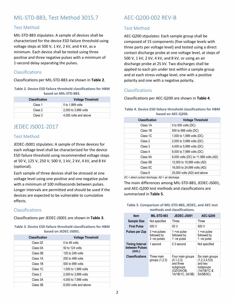
MIL-STD-883, Test Method 3015.7
Test Method
MIL-STD-883 stipulates: A sample of devices shall be
characterized for the device ESD failure threshold using
voltage steps at 500 V, 1 kV, 2 kV, and 4 kV, as a
minimum. Each device shall be tested using three
positive and three negative pulses with a minimum of
1-second delay separating the pulses.
Classifications
Classifications per MIL-STD-883 are shown in Table 2.
Table 2. Device ESD failure threshold classifications for HBM based on MIL-STD-883.
Classification Voltage Threshold
Class 1 0 to 1,999 volts
Class 2 2,000 to 3,999 volts
Class 3
4,000 volts and above
JEDEC JS001-2017
Test Method
JEDEC-JS001 stipulates: A sample of three devices for
each voltage level shall be characterized for the device
ESD failure threshold using recommended voltage steps
at 50 V, 125 V, 250 V, 500 V, 1 kV, 2 kV, 4 kV, and 8 kV
(optional).
Each sample of three devices shall be stressed at one
voltage level using one positive and one negative pulse
with a minimum of 100 milliseconds between pulses.
Longer intervals are permitted and should be used if the
devices are expected to be vulnerable to cumulative
effects.
Classifications
Classifications per JEDEC-JS001 are shown in Table 3.
Table 3. Device ESD failure threshold classifications for HBM based on JEDEC-JS001.
Classification Voltage Threshold
Class 0Z 0 to 49 volts
Class 0A 50 to 124 volts
Class 0B 125 to 249 volts
Class 1A 250 to 499 volts
Class 1B 500 to 999 volts
Class 1C 1,000 to 1,999 volts
Class 2 2,000 to 3,999 volts
Class 3A 4,000 to 7,999 volts
Class 3B 8,000 volts and above
AEC-Q200-002 REV-B
Test Method
AEC-Q200 stipulates: Each sample group shall be
composed of 15 components (five voltage levels with
three parts per voltage level) and tested using a direct
contact discharge probe at one voltage level, at steps of
500 V, 1 kV, 2 kV, 4 kV, and 8 kV, or using an air
discharge probe at 25 kV. Two discharges shall be
applied to each pin under test within a sample group
and at each stress voltage level, one with a positive
polarity and one with a negative polarity.
Classifications
Classifications per AEC-Q200 are shown in Table 4.
Table 4. Device ESD failure threshold classifications for HBM based on AEC-Q200.
Classification Voltage Threshold
Class 1A 0 to 500 volts (DC)
Class 1B 500 to 999 volts (DC)
Class 1C 1,000 to 1,999 volts (DC)
Class 2 2,000 to 3,999 volts (DC)
Class 3 4,000 to 5,999 volts (DC)
Class 4 6,000 to 7,999 volts (DC)
Class 5A 8,000 volts (DC) to 11,999 volts (AD)
Class 5B 12,000 to 15,999 volts (AD)
Class 5C 16,000 to 24,999 volts (AD)
Class 6 25,000 volts (AD) and above
DC = direct contact discharge; AD = air discharge.
The main differences among MIL-STD-883, JEDEC-JS001,
and AEC-Q200 test methods and classifications are
summarized in Table 5.
Table 5. Comparison of MIL-STD-883, JEDEC, and AEC test methods and classifications.
Item MIL-STD-883 JEDEC-JS001 AEC-Q200
Sample Size Not specified Three Three
First Pulse 500 V 50 V 500 V
Pulses per Zap 3 +ve pulses followed by 3 -ve pulses
1 +ve pulse followed by 1 -ve pulse
1 +ve pulse followed by 1 -ve pulse
Timing Interval between Pulses
(min.)
1 second 0.3 second Not specified
Classifications
Three main groups (1,2,3)
Four main groups (0,1,2,3) and three subgroups (OZ/OA/OB, 1A/1B/1C, 3A/3B)
Six main groups (1,2,3,4,5,6) and two subgroups (1A/1B/1C & 5A/5B/5C)

3
Experimental Results
The device under test (DUT) selected for this
experiment was an octal digital driver fabricated using a
rad-hard 1.2-µm complementary metal-oxide-
semiconductor (CMOS) technology. This is a common
driver chip used in several NASA Jet Propulsion
Laboratory (JPL) projects. All of the DUT parts were
sourced with the same date/lot code and tested by the
same test vendor with the same test procedure and
hardware. The HBM test was based on a two-terminal
zap apparatus where one terminal was always
connected to a virtual switching system (VSS) while the
other terminal was applied to the specific test pin of the
DUT with other remaining pins floated. Proper HBM-
specific waveform calibrations were also performed
prior to the start of the experiment.
First HBM Trial: MIL-STD-883 and JEDEC-JS001
A first trial was conducted on this octal driver chip using
a common initial 250-V step following test procedures
for both MIL-STD-883 and JEDEC-JS001 methods.
Table 6 summarizes the experimental results and
observations. The test was conducted under “stop-
after-failure” criteria. One can conclude that the
majority of the parts failed after the 250-V step per
MIL-STD-883 and JEDEC-JS001 classifications. The failure
criterion is defined as a ±15% tolerance in measured
currents between pre- and post-zapped two-terminal
current–voltage (IV) characterization.
Table 6. Summary of first HBM trial (250-V pulse step).
Method Results
MIL-STD-883 Three parts failed after 250 V
JEDEC Two parts failed after 250 V
One part failed after 500 V
Second Trial: MIL-STD-883
A second experiment was then designed with smaller
pulse steps—an initial voltage step of 50 V with 100-V
increments in the subsequent zaps: 50 V, 100 V, 200 V.
Table 7 summarizes the results of the second trial-run
HBM test based on MIL-STD-883. Two parts (M1 and
M2) exhibited fairly gross HBM ESD failures over a
majority of the pins. Part M3 showed that it could
handle the 200-V (max.) zaps across all its pins. Another
common failure signature showed in Table 6 is that
Pins 1–9 of the three parts consistently failed after the
HBM zaps.
Table 7. MIL-STD 883–based test results.
4
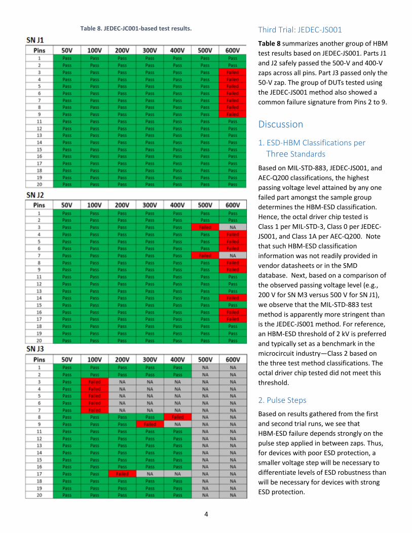
Third Trial: JEDEC-JS001
Table 8 summarizes another group of HBM
test results based on JEDEC-JS001. Parts J1
and J2 safely passed the 500-V and 400-V
zaps across all pins. Part J3 passed only the
50-V zap. The group of DUTs tested using
the JEDEC-JS001 method also showed a
common failure signature from Pins 2 to 9.
Table 8. JEDEC-JC001-based test results.
Discussion
1. ESD-HBM Classifications per
Three Standards
Based on MIL-STD-883, JEDEC-JS001, and
AEC-Q200 classifications, the highest
passing voltage level attained by any one
failed part amongst the sample group
determines the HBM-ESD classification.
Hence, the octal driver chip tested is
Class 1 per MIL-STD-3, Class 0 per JEDEC-
JS001, and Class 1A per AEC-Q200. Note
that such HBM-ESD classification
information was not readily provided in
vendor datasheets or in the SMD
database. Next, based on a comparison of
the observed passing voltage level (e.g.,
200 V for SN M3 versus 500 V for SN J1),
we observe that the MIL-STD-883 test
method is apparently more stringent than
is the JEDEC-JS001 method. For reference,
an HBM-ESD threshold of 2 kV is preferred
and typically set as a benchmark in the
microcircuit industry—Class 2 based on
the three test method classifications. The
octal driver chip tested did not meet this
threshold.
2. Pulse Steps
Based on results gathered from the first
and second trial runs, we see that
HBM-ESD failure depends strongly on the
pulse step applied in between zaps. Thus,
for devices with poor ESD protection, a
smaller voltage step will be necessary to
differentiate levels of ESD robustness than
will be necessary for devices with strong
ESD protection.
5
3. Weak HBM-ESD Protection
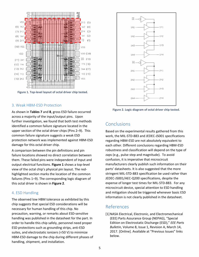
As shown in Tables 7 and 8, gross ESD failure occurred
across a majority of the input/output pins. Upon
further investigation, we found that both test methods
identified a common failure signature located in the
upper section of the octal driver chips (Pins 2─9). This
common failure signature suggests a weak ESD
protection network was implemented against HBM-ESD
damage for this octal driver chip.
A comparison between the pin definitions and pin
failure locations showed no direct correlation between
them. These failed pins were independent of Input and
output electrical functions. Figure 1 shows a top-level
view of the octal chip’s physical pin layout. The red-
highlighted section marks the location of the common
failures (Pins 1–9). The corresponding logic diagram of
this octal driver is shown in Figure 2.
Figure 1. Top-level layout of octal driver chip tested.
Figure 2. Logic diagram of octal driver chip tested.
4. ESD Handling
The observed low HBM tolerance as exhibited by this
chip suggests that special ESD considerations will be
necessary for human handling of this chip. No
precaution, warning, or remarks about ESD-sensitive
handling was published in the datasheet for the part. In
order to handle this chip safely, personnel need proper
ESD protections such as grounding strips, anti-ESD
suites, and electrostatic ionizers (<50 V) to minimize
HBM-ESD damage to the chip during different phases of
handling, shipment, and installation.
Conclusions
Based on the experimental results gathered from this
work, the MIL-STD-883 and JEDEC-JS001 specifications
regarding HBM-ESD are not absolutely equivalent to
each other. Different conclusions regarding HBM-ESD
robustness and classification will depend on the type of
zaps (e.g., pulse step and magnitude). To avoid
confusion, it is imperative that microcircuit
manufacturers clearly publish such information on their
parts’ datasheets. It is also suggested that the more
stringent MIL-STD-883 specification be used rather than
JEDEC-JS001/AEC-Q200 specifications, despite the
expense of longer test times for MIL-STD-883. For any
microcircuit device, special attention to ESD handling
and mitigation should be triggered whenever basic ESD
information is not clearly published in the datasheet.
References
[1] NASA Electrical, Electronic, and Electromechanical (EEE) Parts Assurance Group (NEPAG), “Special Edition on Electrostatic Discharge (ESD),” EEE Parts Bulletin, Volume 8, Issue 1, Revision A, March 14, 2017. [Online]. Available at “Previous Issues” links below.

6
[2] NEPAG, “Second Special Edition on Electrostatic Discharge (ESD),” EEE Parts Bulletin, Volume 9, Issue 1, June 16, 2017. [Online]. Available at “Previous Issues” links below.
[3] NEPAG, “Third Special Edition on Electrostatic Discharge (ESD),” EEE Parts Bulletin, Volume 10, Issue 1, July 17, 2018. [Online]. Available at “Previous Issues” links below.
[4] NEPAG, “Compendium Special Edition on Electrostatic Discharge (ESD),” EEE Parts Bulletin, Volume 10, Issue 2, April 30, 2019, [Online]. Available at “Previous Issues” links below.
[5] Electrostatic Discharge Sensitivity Classification, MIL-STD-883, Method 3015.7, Defense Logistics Agency, Columbus, Ohio, 22 March 1989. [Online]. Available: https://landandmaritimeapps.dla.mil/Programs/MilSpec/ListDocs.aspx?BasicDoc=MIL-STD-883
[6] ESDA/JEDEC Joint Standard for Electrostatic Discharge Sensitivity Testing—Human Body Model (HBM)—Component Level, ANSI/ESDA/JEDEC JS-001-2017, (This is a revision of JEDEC-JS-001-2014, which supersedes and replaces JESD22-A114F.)
[7] Electrostatic Discharge (ESD) Sensitivity Testing Human Body Model (HBM). JESD22-A114F, JEDEC Solid State Technology Association, December 2008.
[8] Human Body Model Electrostatic Discharge Test, AEC-Q200-002 REV-B, Automotive Electronics Council, 2010. [Online]. Available: http://www.aecouncil.com/Documents/AEC_Q200-002B.pdf
Contacts
Peter Majewicz, NEPP Manager [email protected]
Jonathan Pellish, NEPP Deputy Manager & NASA-EEE Parts Manager [email protected]
Shri Agarwal, NEPAG Coordinator 818-354-5598 [email protected]
Michael Han 281-770-7604 [email protected]
Dori Gallagher [email protected]
Brandon Bodkin [email protected]
Robert Evans [email protected]
Armian Hanelli [email protected]
Shayena Khandker [email protected]
Erick Kim [email protected]
Nazia Ovee [email protected]
Claire Marie-Peterson [email protected]
ATPO Doug Sheldon [email protected]
JPL Electronic Parts http://parts.jpl.nasa.gov
Mohammad M. Mojarradi [email protected]
Jeremy L. Bonnell [email protected]
PREVIOUS ISSUES
NASA OSMA EEE Parts: https://sma.nasa.gov/sma-disciplines/eee-parts
Other NASA Centers: https://nepp.nasa.gov/
Public Link (Best with Internet Explorer): https://trs.jpl.nasa.gov/handle/2014/41402
Reference herein to any specific commercial product,
process, or service by trade name, trademark,
manufacturer, or otherwise, does not constitute or
imply its endorsement by the United States
Government or the Jet Propulsion Laboratory, California
Institute of Technology.
www.nasa.gov National Aeronautics and Space Administration
Jet Propulsion Laboratory California Institute of Technology Pasadena, California
© 2020 California Institute of Technology. Government sponsorship acknowledged.