Comparison of OQPSK and CPM for Communications at 60GHz ...
14
Hindawi Publishing Corporation EURASIP Journal on Wireless Communications and Networking Volume 2007, Article ID 86206, 14 pages doi:10.1155/2007/86206 Research Article Comparison of OQPSK and CPM for Communications at 60 GHz with a Nonideal Front End Jimmy Nsenga, 1, 2 Wim Van Thillo, 1, 2 Franc ¸ois Horlin, 1 Andr ´ e Bourdoux, 1 and Rudy Lauwereins 1, 2 1 IMEC, Kapeldreef 75, 3001 Leuven, Belgium 2 Departement Elektrotechniek - ESAT, Katholieke Universiteit Leuven, Kasteelpark Arenberg 10, 3001 Leuven, Belgium Received 4 May 2006; Revised 14 November 2006; Accepted 3 January 2007 Recommended by Su-Khiong Yong Short-range digital communications at 60GHz have recently received a lot of interest because of the huge bandwidth available at those frequencies. The capacity offered to the users could finally reach 2 Gbps, enabling the deployment of new multimedia applications. However, the design of analog components is critical, leading to a possible high nonideality of the front end (FE). The goal of this paper is to compare the suitability of two different air interfaces characterized by a low peak-to-average power ratio (PAPR) to support communications at 60GHz. On one hand, we study the offset-QPSK (OQPSK) modulation combined with a channel frequency-domain equalization (FDE). On the other hand, we study the class of continuous phase modulations (CPM) combined with a channel time-domain equalizer (TDE). We evaluate their performance in terms of bit error rate (BER) considering a typical indoor propagation environment at 60 GHz. For both air interfaces, we analyze the degradation caused by the phase noise (PN) coming from the local oscillators; and by the clipping and quantization errors caused by the analog-to-digital converter (ADC); and finally by the nonlinearity in the PA. Copyright © 2007 Jimmy Nsenga et al. This is an open access article distributed under the Creative Commons Attribution License, which permits unrestricted use, distribution, and reproduction in any medium, provided the original work is properly cited. 1. INTRODUCTION We are witnessing an explosive growth in the demand for wireless connectivity. Short-range wireless links like wire- less local area networks (WLANs) and wireless personal area networks (WPANs) will soon be expected to deliver bit rates of over 1 Gbps to keep on satisfying this demand. Fast wireless download of multimedia content and stream- ing high-definition TV are two obvious examples. As lower frequencies (below 10 GHz) are getting completely congested though, bandwidth for these Gbps links has to be sought at higher frequencies. Recent regulation assigned a 3 GHz wide, worldwide available frequency band at 60 GHz to this kind of applications [1]. Communications at 60 GHz have some advantages as well as some disadvantages. The main advantages are three- fold. The large unlicensed bandwidth around 60 GHz (more than 3 GHz wide) will enable very high data rate wireless ap- plications. Secondly, the high free space path loss and high attenuation by walls simplify the frequency reuse over small distances. Thirdly, as the wavelength in free space is only 5 mm, the analog components can be made small. Therefore, on a small area, one can design an array of antennas, which steers the beam in a given target direction. This improves the link budget and reduces the time dispersion of the channel. Opposed to this are some disadvantages: the high path loss will restrict communications at 60 GHz to short distances, more stringent requirements are put on the analog com- ponents (like multi-Gsamples/s analog-to-digital converter ADC), and nonidealities of the radio frequency (RF) front end have a much larger impact than at lower frequencies. The design of circuits at millimeter waves is more problematic than at lower frequencies for two important reasons. First, the operating frequency is relatively close to the cut-off fre- quency and to the maximum oscillation frequency of nowa- days’ complementary metal oxide semiconductor (CMOS) transistors (e.g., the cut-off frequency of a transistor in a 90 nm state-of-the-art CMOS is around 150 GHz [2]), reduc- ing significantly the design freedom. Second, the wavelength approaches the size of on-chip dimensions so that the inter- connects have to be modeled as (lossy) transmission lines, complicating the modeling and circuit simulation and also the layout of the chip. A suitable air interface for low-cost, low-power 60 GHz transceivers should thus use a modulation technique that has a high level of immunity to FE nonidealities (especially phase
Transcript of Comparison of OQPSK and CPM for Communications at 60GHz ...

Hindawi Publishing CorporationEURASIP Journal on Wireless Communications and NetworkingVolume 2007, Article ID 86206, 14 pagesdoi:10.1155/2007/86206
Research ArticleComparison of OQPSK and CPM for Communications at60 GHz with a Nonideal Front End
Jimmy Nsenga,1, 2 Wim Van Thillo,1, 2 Francois Horlin,1 Andre Bourdoux,1 and Rudy Lauwereins1, 2
1 IMEC, Kapeldreef 75, 3001 Leuven, Belgium2 Departement Elektrotechniek - ESAT, Katholieke Universiteit Leuven, Kasteelpark Arenberg 10, 3001 Leuven, Belgium
Received 4 May 2006; Revised 14 November 2006; Accepted 3 January 2007
Recommended by Su-Khiong Yong
Short-range digital communications at 60 GHz have recently received a lot of interest because of the huge bandwidth availableat those frequencies. The capacity offered to the users could finally reach 2 Gbps, enabling the deployment of new multimediaapplications. However, the design of analog components is critical, leading to a possible high nonideality of the front end (FE).The goal of this paper is to compare the suitability of two different air interfaces characterized by a low peak-to-average powerratio (PAPR) to support communications at 60 GHz. On one hand, we study the offset-QPSK (OQPSK) modulation combinedwith a channel frequency-domain equalization (FDE). On the other hand, we study the class of continuous phase modulations(CPM) combined with a channel time-domain equalizer (TDE). We evaluate their performance in terms of bit error rate (BER)considering a typical indoor propagation environment at 60 GHz. For both air interfaces, we analyze the degradation caused bythe phase noise (PN) coming from the local oscillators; and by the clipping and quantization errors caused by the analog-to-digitalconverter (ADC); and finally by the nonlinearity in the PA.
Copyright © 2007 Jimmy Nsenga et al. This is an open access article distributed under the Creative Commons Attribution License,which permits unrestricted use, distribution, and reproduction in any medium, provided the original work is properly cited.
1. INTRODUCTION
We are witnessing an explosive growth in the demand forwireless connectivity. Short-range wireless links like wire-less local area networks (WLANs) and wireless personalarea networks (WPANs) will soon be expected to deliverbit rates of over 1 Gbps to keep on satisfying this demand.Fast wireless download of multimedia content and stream-ing high-definition TV are two obvious examples. As lowerfrequencies (below 10 GHz) are getting completely congestedthough, bandwidth for these Gbps links has to be sought athigher frequencies. Recent regulation assigned a 3 GHz wide,worldwide available frequency band at 60 GHz to this kind ofapplications [1].
Communications at 60 GHz have some advantages aswell as some disadvantages. The main advantages are three-fold. The large unlicensed bandwidth around 60 GHz (morethan 3 GHz wide) will enable very high data rate wireless ap-plications. Secondly, the high free space path loss and highattenuation by walls simplify the frequency reuse over smalldistances. Thirdly, as the wavelength in free space is only5 mm, the analog components can be made small. Therefore,on a small area, one can design an array of antennas, which
steers the beam in a given target direction. This improves thelink budget and reduces the time dispersion of the channel.Opposed to this are some disadvantages: the high path losswill restrict communications at 60 GHz to short distances,more stringent requirements are put on the analog com-ponents (like multi-Gsamples/s analog-to-digital converterADC), and nonidealities of the radio frequency (RF) frontend have a much larger impact than at lower frequencies. Thedesign of circuits at millimeter waves is more problematicthan at lower frequencies for two important reasons. First,the operating frequency is relatively close to the cut-off fre-quency and to the maximum oscillation frequency of nowa-days’ complementary metal oxide semiconductor (CMOS)transistors (e.g., the cut-off frequency of a transistor in a90 nm state-of-the-art CMOS is around 150 GHz [2]), reduc-ing significantly the design freedom. Second, the wavelengthapproaches the size of on-chip dimensions so that the inter-connects have to be modeled as (lossy) transmission lines,complicating the modeling and circuit simulation and alsothe layout of the chip.
A suitable air interface for low-cost, low-power 60 GHztransceivers should thus use a modulation technique that hasa high level of immunity to FE nonidealities (especially phase

2 EURASIP Journal on Wireless Communications and Networking
noise (PN) and ADC quantization and clipping), and allowsan efficient operation of the power amplifier (PA). Since the60 GHz channel has been shown to be frequency selectivefor very large bandwidths and low antenna gains [3, 4], or-thogonal frequency division multiplexing (OFDM) has beenproposed for communications at 60 GHz. However, it is verysensitive to nonidealities such as PN and carrier frequencyoffset (CFO). Moreover, due to its high PAPR, it requires thePA to be backed off by several dB more than for a single car-rier (SC) system, thus lowering the power efficiency of thesystem.
Therefore, we consider two other promising air interfacesthat relax the FE requirements. First, we study an SCtransmission scheme combined with OQPSK because ithas a lower PAPR than regular QPSK or QAM in band-limited channels. As the multipath channel should beequalized at a low complexity, we add redundancy at thetransmitter to make the signal cyclic and to be able toequalize the channel in the frequency domain [5]. Sec-ondly, we study CPM techniques [6]. These have a per-fectly constant amplitude, or a PAPR of 0 dB. Moreover,their continuous phase property results in lower spectralsidelobes. Linear representations and approximations de-veloped by Laurent [7] and Rimoldi [8] allow for greatcomplexity reductions in the equalization and detectionprocesses. In order to mitigate the multipath channel,a conventional convolutive zero-forcing (ZF) equalizer isused.
The goal of this paper is to analyze, by means of simula-tions, the impact of three of the most critical building blocksin RF transceivers, and to compare the robustness of the twoair interfaces to their nonideal behavior:
(i) the mixing stage where the local oscillator PN can bevery high at 60 GHz,
(ii) the ADC that, for low-power consumption, must havethe lowest possible resolution (number of bits) giventhe very high bit rate,
(iii) the PA where nonlinearities cause distortion and spec-tral regrowth.
The paper is organized as follows. In Section 2, we de-scribe the indoor channel at 60 GHz. Section 3 describesthe considered FE nonidealities. Sections 4 and 5 intro-duce the OQPSK and CPM air interfaces, respectively, to-gether with their receiver design. Simulation setup and re-sults are provided in Section 6 and the conclusions are drawnin Section 7.
Notation
We use roman letters to represent scalars, single underlinedletters to denote column vectors, and double underlined let-ters to represent matrices. [·]T and [·]H stand for trans-pose and complex conjugate transpose operators, respec-tively. The symbol � denotes the convolution operation and⊗ the Kronecker product. I
kis the identity matrix of size
k × k and 0m×n is an m × n matrix with all entries equal
to 0.
2. THE INDOOR 60 GHZ CHANNEL
2.1. Propagation characteristics
The interest in the 60 GHz band is motivated by the largeamount of unlicensed bandwidth located between 57 and64 GHz [1, 9]. Analyzing the spectrum allocation in theUnited States (US), Japan, and Europe, one notices that thereis a common contiguous 3 GHz bandwidth between 59 and62 GHz that has been reserved for high data rate applications.This large amount of bandwidth can be exploited to establisha wireless connection at more than 1 Gbps.
Different measurement campaigns have been carried outto characterize the 60 GHz channel. The free space loss (FSL)can be computed using the Friis formula (1) as follows:
FSL [dB] = 20× log10
(4πdλ
), (1)
where λ is signal wavelength and d is the distance of the ter-minal from the transmitter base station. One can see that theFLS is already 68 dB at 1 m separation away from the trans-mitter. Thus, given the limited transmitted power, the com-munication range will hardly extend over 10 m. Besides theFSL, reflection and penetration losses of objects at 60 GHzare higher than at lower frequencies [10, 11]. For instance,concrete walls 15 cm thick attenuate the signal by 36 dB. Theyact thus as real boundaries between different rooms.
However, the signals reflected off the concrete walls havea sufficient amplitude to contribute to the total receivedpower, thus making the 60 GHz channel a multipath chan-nel [3, 12]. Typical root mean-square (RMS) delay spreads at60 GHz can vary from 10 nanoseconds to 100 nanosecondsif omni-directional antennas are used, depending on the di-mensions and reflectivity of the environment [3]. However,the RMS delay spread can be greatly reduced to less than 1nanosecond by using directional antennas, thus increasingthe coherence bandwidth of the channel up to 200 MHz [13].
Moreover, the objects moving within the communica-tion environment make the channel variant over time. Typ-ical values of Doppler spread at 60 GHz are around 200 Hzat a normal walking speed of 1 millisecond. This results ina coherence time of approximatively 1 millisecond. With asymbol period of 1 nanosecond, 106 symbols can be trans-mitted in a quasistatic environment. Thus, Doppler spreadat 60 GHz will not have a significant impact on the systemperformance.
In summary, 60 GHz communications are mainly suit-able for short-range communications due to the high prop-agation loss. The channel is frequency selective due to thelarge bandwidth used (more than 1 GHz). However, one canassume the channel to be time invariant during the transmis-sion of one block.
2.2. Channel model
In this study, we model the indoor channel at 60 GHz us-ing the Saleh-Valenzuela model [14], which assumes that the

Jimmy Nsenga et al. 3
received signals arrive in clusters. The rays within a clusterhave independent uniform phases. They also have indepen-dent Rayleigh amplitudes whose variances decay exponen-tially with cluster and rays delays. In the Saleh-Valenzuelamodel, the cluster decay factor is denoted by Γ and the raysdecay factor is represented by γ. The clusters and the raysform Poisson arrival processes that have different, but fixedrates Λ and λ, respectively [14].
We consider the same scenario as that defined in [15].The base station has an omni-directional antenna with 120◦
beam width and is located in the center of the room. The re-mote station has an omni-directional antenna with 60◦ beamwidth and is placed at the edge of the room. The correspond-ing Saleh-Valenzuela parameters are presented in Table 1.
3. NONIDEALITIES IN ANALOG TRANSCEIVERS
In this section, we introduce 3 FE nonidealities: ADC clip-ping and quantization, PN and nonlinearity of the PA. Therationale for choosing these 3 nonidealities is that a good PA,a high resolution ADC, and a low PN oscillator have a highpower consumption [16].
3.1. Clipping and quantization
3.1.1. Motivation
The number of bits (NOB) of the ADC must be kept as lowas possible for obvious reasons of cost and power consump-tion. On the other hand, a large number of bits is desirableto reduce the effect of quantization noise and the risk of clip-ping the signal. Clipping occurs when the signal fluctuationis larger than the dynamic range of the ADC. Without goinginto detail, we mention that there is always an optimal clip-ping level for a given NOB. As the clipping level is increased,the signal degradation due to clipping is reduced. However,the degradation due to quantization is increased as a largerdynamic range must be covered with the same NOB. For amore elaborate discussion, we refer to [17].
3.1.2. Model
The ADC is thus characterized by two parameters: the NOBand the normalized clipping level μ, which is the ratio of theclipping level to the RMS value of the amplitude of the signal.In Figure 1, we illustrate the clipping/quantization functionfor an NOB = 3. This simple model is used in our simula-tions in Section 6.4.
3.2. Phase noise
3.2.1. Motivation
PN originates from nonideal clock oscillators, voltagecon-trolled oscillators (VCO), and frequency synthesis circuits.In the frequency domain, PN is most often characterized bythe power spectral density (PSD) of the the oscillator phaseφ(t). The PSD of an ideal oscillator has only a Dirac pulse atits carrier frequency, corresponding to no phase fluctuation
Table 1: Saleh-Valenzuela channel parameters at 60 GHz.
1/Λ 75 nanoseconds
Γ 20 nanoseconds
1/λ 5 nanoseconds
γ 9 nanoseconds
Normalized Vout
Normalized Vin
[Vin
RMS(Vin)
]
−μ
Figure 1: ADC input-output characteristic.
at all. In practice, the PSD of the phase exhibits a 20 dB/decdecreasing behavior as the offset from the carrier frequencyincreases. Nonmonotonic behavior is attributable to, for ex-ample, phase-locked loop (PLL) filters in the frequency syn-thesis circuit.
3.2.2. Model
We characterize the phase noise by a set of 3 parameters (seeFigure 2) [18]:
(i) the integrated PSD denotedK , expressed in dBc, whichis the two-sided integral of the phase noise PSD,
(ii) the 3 dB bandwidth,(iii) the VCO noise floor.
Note that these 3 parameters will fix the value of the PN PSDat low frequency offsets. In our simulations (see Section 6.3),we assume a phase noise bandwidth of 1 MHz and a noisefloor of −130 dBc/Hz. Typical values of the level of PN PSDat 1 MHz are considered [19] and the corresponding inte-grated PSD is calculated in Table 2. In order to generate aphase noise characterized by the PSD illustrated in Figure 2,a white Gaussian noise is convolved with a filter whose fre-quency domain response is equal to the square root of thePSD.
3.3. Nonlinear power amplification
3.3.1. Motivation
Nonlinear behavior can occur in any amplifier but it is morelikely to occur in the last amplifier of the transmitter wherethe signal power is the highest. For power consumption rea-sons, this amplifier must have a saturated output power thatis as low as possible, compatible with the system level con-straints such as transmit power and link budget. The gaincharacteristic of an amplifier is almost perfectly linear at low

4 EURASIP Journal on Wireless Communications and Networking
Table 2: Simulated integrated PSD.
PN @1 MHz [dBc/Hz] Integrated PSD [dBc]
−90 −24
−85 −20
−82 −16
10G
Hz
1G
Hz
100
MH
z
10M
Hz
1M
Hz
100
kHz
10kH
z
1kH
z
100
Hz
10H
z
Offset from carrier
−140
−130
−120
−110
−100
−90
−80
−70
Ph
ase
noi
seP
SD[d
Bc/
Hz]
3 dB cut-off
−20 dB/decade
Noise floor
Figure 2: Piecewise linear phase noise PSD definition used in thephase noise model.
input level and, for increasing input power, deviates fromthe linear behavior as the input power approaches the 1-dBcompression point (P1 dB: the point at which the gain is re-duced by 1-dB because the amplifier is driven into satura-tion) and eventually reaches complete saturation. The inputthird-order intercept point (IP3) is also often used to quan-tify the nonlinear behavior of amplifiers. It is the input powerat which the power of the two-tone third-order intermodu-lation product would become equal to the power of the first-order term. When peaks are present in the transmitted wave-form, one has to operate the PA with a few dBs of backoff toprevent distortion. This backoff actually reduces the powerefficiency of the PA and must be kept to a minimum.
3.3.2. Model
In our simulation (see Section 6.5), we characterize the non-linearity of the PA by a third-order nonlinear equation
y(t) = a1x(t) + a3∣∣x(t)
∣∣2x(t), (2)
where x(t) and y(t) are the baseband equivalent PA inputand output, respectively, a1 and a3 are real polynomial coef-ficients. We assume an amplifier with a unity gain (a1 = 1)and an input amplitude at 1-dB compression point A1dB nor-malized to 1. Therefore, by using (3), one can compute thethird-order coefficient a3
a3 = −0.145a1
A21 dB
. (3)
Ain1xRMS
Backoff > 0
yRMS
1
Aout
1 dB
Figure 3: PA input-output power characteristic.
The parameter a3 is then equal to −0.145. Note that (2)models only the amplitude-to-amplitude (AM-AM) conver-sion of a nonlinear PA. In order to make our model morerealistic, a saturation level is set from the extremum of thecubic function. The root mean-square (RMS) value of the in-put PA signal is computed and its level is adapted accordingto the backoff requirement. The backoff is defined relative toA1 dB and is the only varying parameter. Then the nonlinear-ity is introduced using the AM-AM conversion as shown inFigure 3.
4. OFFSET QPSK WITH FREQUENCYDOMAIN EQUALIZATION
4.1. Initial concept
Offset-QPSK, a variant of QPSK digital modulation, is char-acterized by a half symbol period delay between the datamapped on the quadrature (Q) branch and the one mappedon the inphase (I) branch. This offset imposes that either theI or theQ signal changes during the half symbol period. Con-sequently, the phase shift between two consecutive OQPSKsymbols is limited to ±90◦ (±180◦ in conventional QPSKmodulation), thus avoiding the amplitude of the signal to gothrough the “0” point. The advantage of an OQPSK mod-ulated signal over QPSK signal is observed in band-limitedchannels where nonrectangular pulse shaping, for instance,root raised root cosine, is used. The envelope fluctuation ofan OQPSK signal is found to be 70% lower than that of aconventional QPSK signal [20]. Thus, OQPSK is consideredto be a low PAPR modulation scheme, for which a nonlinearPA with less backoff can be used, thus increasing the powerefficiency of the system.
4.2. System model
Our system model is inspired from the model of Wang andGiannakis [21]. Let us consider the baseband block trans-mitter model represented in Figure 4. The inphase compo-nent of the digital OQPSK signal is denoted by uI[k] and

Jimmy Nsenga et al. 5
uI [k]
uQ[k]
S/P
S/P
uI [k]
uQ[k]Tcp
Tcp
xI [k]
xQ[k]
P/S
P/S
xI [k]
xQ[k]gTQ(t)
gTI (t)
× j
s(t)
Figure 4: Offset QPSK block transmission.
the quadrature-phase component denoted by uQ[k]. The twostreams are first serial-to-parallel (S/P) converted to formblocks uI[k] := [uI[kB],uI[kB + 1], . . . ,uI[kB + B − 1]]T
and uQ[k] := [uQ[kB],uQ[kB + 1], . . . ,uQ[kB + B − 1]]T
where B is the block size. Then, a cyclic prefix (CP) of lengthNcp is inserted at the beginning of each block to get cyclicblocks xI[k] and xQ[k]. The cyclic prefix insertion is doneby multiplying both uI[k] and uQ[k] with the matrix T
cp=
[0Ncp×(B−Ncp)
, INcp
; IB
] of size (B +Ncp)×B. In a practical sys-
tem, the Ncp should be larger than the channel impulse re-sponse length, and the size of the block B is chosen so thatthe CP overhead is limited (practically an overhead of 1/5 isoften used). The size B should on the other hand be as smallas possible to reduce the complexity and to ensure that thechannel is constant within one symbol block duration. Thecyclic blocks xI[k] and xQ[k] are afterwards converted backto serial streams and the resulting streams xI[k] and xQ[k] ofsample duration equal to T are filtered by square root raisedcosine filters gTI (t) and gTQ(t), respectively. The inherent offsetbetween I and Q branches, which differentiates the OQPSKsignaling from the normal QPSK, is modeled through thepulse-shaping filters defined such that gTQ(t) = gTI (t − T/2).The two pulse-shaped signals are then summed together toform the equivalent complex lowpass transmitted signal s(t).
The signal s(t) is then transmitted through a frequencyselective channel, which we model by its equivalent lowpasschannel impulse response c(t). Figure 5 shows a block dia-gram of the receiver. The received signal rin(t) is corruptedby additive white Gaussian noise (AWGN), n(t), generatedby analog FE components. The noisy received signal is firstlowpass-filtered by an anti-aliasing filter with ideal lowpassspecifications before the discretization. We consider the fol-lowing two sample rates.
(i) The nonfractional sampling (NFS) rate which corre-sponds to sampling the analog signal every T seconds.The corresponding anti-aliasing filter, denoted gRNFS(t),eliminates all the frequencies above 0.5/T .
(ii) The fractional sampling (FS) rate for which the sam-pling period is T/2 seconds. The cutoff frequency ofthe anti-aliasing filter gRFS(t) is set to 1/T .
More information about the two sampling modes can befound in [22]. In the sequel, we focus on the FS case. TheNFS can be seen as a special case of FS. In order to character-ize the received signal, we define hI(t) := gTI (t)�c(t)�gRFS(t)and hQ(t) := j ∗ gTQ(t) � c(t) � gRFS(t) as the overall chan-nel impulse response encountered by data symbols on I andQ, respectively. The received signal after lowpass filtering is
given by
r(t) =∑k
xI[k]hI(t − kT) +∑k
xQ[k]hQ(t − kT) + v(t)
(4)
in which v(t) is the lowpass filtered noise. The analog re-ceived signal r(t) is then sampled every T/2 seconds to getthe discrete-time sequence r[m].
As explained in [22], fractionally sampled signals are pro-cessed by creating polyphase components, where even andodd indexed samples of the received signal are separated. Inthe following, the index “0” is related to even samples orpolyphase component “0” while odd samples are representedby index “1” or polyphase component “1.” Thus, we define
rρ[m]def= r[2m + ρ],
vρ[m]def= v[2m + ρ],
hρI [m]
def= hI[2m + ρ],
hρQ[m]
def= hQ[2m + ρ],
(5)
where ρ denotes either the polyphase component “0” or thepolyphase component “1,” r[m] and v[m] are, respectively,the received signal r(t) and the noise v(t) sampled every T/2seconds, hI[m] and hQ[m] represent the discrete-time ver-sion of, respectively, hI(t) and hQ(t) sampled every T/2 sec-onds. The sampled channels h
ρI [m] and h
ρQ[m] have finite
impulse responses, of length LI and LQ, respectively. Thesetime dispersions cause the intersymbol interference (ISI) be-tween consecutive symbols, which, if not mitigated, degradesthe performance of the system. Next to the separation inpolyphase components, we separate the real and imaginaryparts of different polyphase signals. Starting from now, weuse the supplementary upper index c = {r, i} to identify thereal or imaginary parts of the sequences.
The four real-valued sequences rρc[m] are serialto parallel converted to obtain the blocks rρc[m] :=[rρc[mB], rρc[mB+1], . . . , rρc[mB+B+Ncp−1]]T of (B+Ncp)samples. The corresponding transmit-receive block relation-ship, assuming a correct time and frequency synchroniza-tion, is given by
rρc[m] = HρcI
[0]TcpuI[m] + Hρc
I[1]T
cpuI[m− 1]
+ HρcQ
[0]TcpuQ[m] + Hρc
Q[1]T
cpuQ[m− 1]
+ vρc[m],
(6)
where vρc[m] is the mth filtered noise block defined asvρc[m] := [vρc[mB], vρc[mB+1], . . . , vρc[mB+B+Ncp−1]]T .The square matrices Hρc
X[0] and Hρc
X[1] of size (B+Ncp)×(B+
Ncp), with X equal to I or Q, are represented in the following

6 EURASIP Journal on Wireless Communications and Networking
rin(t)
n(t)
gRNFS(t)
T
r(t)r[m]
Real
Imag.
S/P
S/P
rr[m]
ri[m]
Rcp
Rcp
yr[m]
yi[m]
rin(t)
n(t)
gRFS(t)
T/2
r(t)r[m]
z−1
2
2
Real
r0[m]
Imag.
Real
r1[m]
Imag.
S/P
S/P
S/P
S/P
r0r[m]
r0i[m]
r1r[m]
r1i[m]
Rcp
Rcp
Rcp
Rcp
y0r[m]
y0i[m]
y1r[m]
y1i[m]
Figure 5: Receiver: upper part NFS, lower part FS.
equations:
HρcX
[0] =
⎡⎢⎢⎢⎢⎢⎢⎢⎢⎢⎣
hρcX [0] 0 0 · · · 0
... hρcX [0] 0 · · · 0
hρcX [LX] · · · . . . · · · 0
.... . . · · · . . . 0
0 · · · hρcX [LX] · · · h
ρcX [0]
⎤⎥⎥⎥⎥⎥⎥⎥⎥⎥⎦
,
HρcX
[1] =
⎡⎢⎢⎢⎢⎢⎢⎢⎢⎢⎣
0 · · · hρcX [LX] · · · h
ρcX [1]
.... . . 0
. . ....
0 · · · . . . · · · hρcX [LX]
...... · · · . . .
...0 · · · 0 · · · 0
⎤⎥⎥⎥⎥⎥⎥⎥⎥⎥⎦.
(7)
The second and the fourth terms in (6) highlight the inter-block interference (IBI) that arises between consecutiveblocks due to the time dispersion of the channel. The IBIbetween consecutive blocks uI[m] or uQ[m] is afterwardseliminated by discarding the first Ncp samples in each re-ceived block. This operation is carried out by multiplyingthe received blocks in (6) by a guard removal matrix R
cp=
[0B×Ncp
, IB
] of size B × (B + Ncp). We get
yρc[m]def= R
cprρc[m] = R
cpHρc
I[0]T
cpuI[m]
+ RcpHρc
I[1]T
cpuI[m− 1] + R
cpHρc
Q[0]T
cpuQ[m]
+ RcpHρc
Q[1]T
cpuQ[m− 1] + R
cpvρc[m].
(8)
AsNcp has been chosen to be larger than the max{LI ,LQ},the product of R
cpand each of Hρc
I[1] and Hρc
Q[1] matri-
ces is null. Moreover, the left and right cyclic prefix inser-tion and removal operations around Hρc
I[0] and Hρc
Q[0], de-
scribed mathematically as RcpHρc
I[0]T
cpand R
cpHρc
Q[0]T
cp,
respectively, result in circulant matrices Hρc
Iand H
ρc
Qof size
(B × B). Finally, the discrete-time block input-output rela-tionship taking the CP insertion and removal operations intoaccount is
yρc[m] = Hρc
IuI[m] + H
ρc
QuQ[m] + wρc[m] (9)
in which wρc[m] is obtained by discarding the first Ncp sam-ples from the filtered noise block vρc[m]. By stacking the realand the imaginary parts of the two polyphase componentson top of each other, the matrix representation of the FS caseis
⎡⎢⎢⎢⎣
y0r[m]y0i[m]y1r[m]y1i[m]
⎤⎥⎥⎥⎦
︸ ︷︷ ︸y[m]
=
⎡⎢⎢⎢⎢⎢⎢⎣
H0r
IH
0r
Q
H0i
IH
0i
Q
H1r
IH
1r
Q
H1i
IH
1i
Q
⎤⎥⎥⎥⎥⎥⎥⎦
︸ ︷︷ ︸H
[uI[m]uQ[m]
]
︸ ︷︷ ︸u[m]
+
⎡⎢⎢⎢⎣w0r[m]w0i[m]w1r[m]w1i[m]
⎤⎥⎥⎥⎦
︸ ︷︷ ︸w[m]
. (10)
Finally, we get
y[m] = H u[m] + w[m] (11)
in which y[m] denotes the compound received signal, u[m]is a vector containing both the I and Q transmitted symbols,and w[m] denotes the noise vector, H is the compound chan-nel matrix. The vectors y[m] and w[m] contain 4B symbols,
H is a matrix of size 4B × 2B, and u[m] is a vector of 2Bsymbols. Notice that all these vectors and matrices are realvalued. Interestingly, the NFS case can be obtained from theFS by the two following adaptations.
(i) First, one has to change the analog anti-aliasing filterat the receiver. In fact, the cut-off frequency of the NFSfilter is 0.5/T while it is 1/T for the FS filter.
(ii) Second, one keeps only the polyphase component withsuperscript index “0” in (10).
Jimmy Nsenga et al. 7
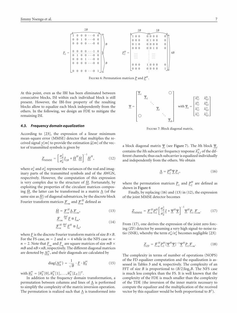
P1 =
2B
B
B
1 0 0 0 · · ·0 00 0 1 0 · · ·0 00 0 0 0 · · ·0 0
0 0 0 0 · · ·1 00 1 0 0 · · ·0 00 0 0 1 · · ·0 00 0 0 0 · · ·0 0
0 0 0 0 · · ·0 1
PH2 =
2B 2B
4B
1 0 0 0 0 0 0 00 0 0 0 1 0 0 00 1 0 0 0 0 0 00 0 0 0 0 1 0 0
. . . . . .
. . . . . .
. . . . . .
0 0 0 1 0 0 0 00 0 0 0 0 0 0 1
Figure 6: Permutation matrices P and PH .
At this point, even as the IBI has been eliminated betweenconsecutive blocks, ISI within each individual block is stillpresent. However, the IBI-free property of the resultingblocks allow to equalize each block independently from theothers. In the following, we design an FDE to mitigate theremaining ISI.
4.3. Frequency domain equalization
According to [23], the expression of a linear minimummean-square error (MMSE) detector that multiplies the re-ceived signal y[m] to provide the estimation u[m] of the vec-tor of transmitted symbols is given by
ZMMSE
=[σ2w
σ2uI
2B+ H
HH]−1
HH
, (12)
where σ2u and σ2
w represent the variances of the real and imag-inary parts of the transmitted symbols and of the AWGN,respectively. However, the computation of this expressionis very complex due to the structure of H . Fortunately, byexploiting the properties of the circulant matrices compos-ing H , the latter can be transformed in a matrix Λ (of thesame size as H) of diagonal submatrices, by the discrete block
Fourier transform matrices Fm
and F Hn
defined as
H = F HnΛF
m, (13)
Fm
def= F ⊗ Im
,
F Hn
def= FH ⊗ In,
(14)
where F is the discrete Fourier transform matrix of size B×B.For the FS case, m = 2 and n = 4 while in the NFS case m =n = 2. Note that F
mand F
nare square matrices of size mB ×
mB and nB×nB, respectively. The different diagonal matricesare denoted by Λρc
X, and their diagonals are calculated by
diag(ΛρcX
) = 1√B· F · hρcX (15)
with hρcX = [h
ρcX [0],h
ρcX [1], . . . ,h
ρcX [LX]]T .
In addition to the frequency domain transformation, apermutation between columns and lines of Λ is performedto simplify the complexity of the matrix inversion operation.The permutation is realized such that Λ is transformed into
Ψ =
⎡⎢⎢⎢⎢⎢⎢⎢⎢⎢⎢⎢⎣
Ψ1
©Ψ
2
. . .Ψ
l
© . . .Ψ
B
⎤⎥⎥⎥⎥⎥⎥⎥⎥⎥⎥⎥⎦
with Ψl=
⎡⎢⎢⎢⎢⎢⎣
λ0rI ,l λ0r
Q,l
λ0iI ,l λ0i
Q,l
λ1rI ,l λ1r
Q,l
λ1iI ,l λ1i
Q,l
⎤⎥⎥⎥⎥⎥⎦
Figure 7: Block diagonal matrix.
a block diagonal matrix Ψ (see Figure 7). The lth block Ψl
contains the lth subcarrier frequency response λρcX ,l of the dif-
ferent channels; thus each subcarrier is equalized individuallyand independently from the others. We obtain
Λ = PH2ΨP
1, (16)
where the permutation matrices P1
and PH2
are defined asshown in Figure 6
Finally, by replacing (16) and (13) in (12), the expressionof the joint MMSE detector becomes
ZMMSE
= F HnPH
2
[σ2w
σ2uI + ΨHΨ
]−1
ΨHP1F
m. (17)
From (17), one derives the expression of the joint zero forc-ing (ZF) detector by assuming a very high signal-to-noise ra-tio (SNR), whereby the term σ2
w/σ2u becomes negligible [23]:
ZZF= F H
nPH
2[ΨHΨ]−1ΨHP
1F
m. (18)
The complexity in terms of number of operations (NOPS)of the FD equalizer computation and the equalization is as-sessed in Tables 3 and 4, respectively. The complexity of anFFT of size B is proportional to (B/2)log2B. The NFS caseis much less complex than the FS. It is well known that thecomplexity of the FDE is much smaller than the complexityof the TDE (the inversion of the inner matrix necessary tocompute the equalizer and the multiplication of the receivedvector by this equalizer would be both proportional to B3).
8 EURASIP Journal on Wireless Communications and Networking
Table 3: Equalizer computation.
Task OperationNOPS
FS NFS
Computation of diag(ΛρcX
) FFT 8 4
Computation of [ΨHΨ]−1ΨH + and × 8B 4B
Table 4: Equalization.
Task OperationNOPS
FS NFS
Frequency components of yρc[m] FFT 4 2
Equalization + and × 14B 6B
Equalized symbols in time domain IFFT 2 2
5. CONTINUOUS PHASE MODULATION
5.1. Transmitted signal
CPM covers a large class of modulation schemes with a con-stant amplitude, defined by
s(t, a) =√
2EST
e jφ(t,a), (19)
where s(t, a) is the sent complex baseband signal, ES theenergy per symbol, T the symbol duration, and a =[a[0], a[1], . . . , a[N − 1]] is a vector of length N con-taining the sequence of M-ary data symbols a[n] =±1,±3, . . . ,±(M − 1). The transmitted information is con-tained in the phase
φ(t, a) = 2πhN−1∑n=0
a[n] · q(t − nT), (20)
where h is the modulation index and
q(t) =∫ t
−∞g(τ)dτ. (21)
Normally the function g(t) is a smooth pulse shape overa finite time interval 0 ≤ t ≤ LT and zero outside. ThusL is the length of the pulse per unit T . The function g(t) isnormalized such that
∫∞−∞ g(t)dt = 1/2. This means that for
schemes with positive pulses of finite length, the maximumphase change over any symbol interval is (M − 1)hπ.
As shown in [24], the BER can be halved by precodingthe information sequence before passing it through the CPMmodulator. If d = [d[1],d[2], . . . ,d[N − 1]] is a vector con-taining the uncoded input bipolar symbol stream, the outputof the precoder a (assuming M = 2) can be written as
a[n] = d[n] · d[n− 1], (22)
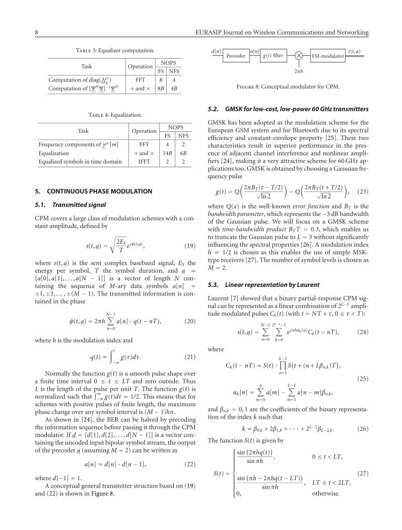
where d[−1] = 1.A conceptual general transmitter structure based on (19)
and (22) is shown in Figure 8.
d[n]Precoder
a[n]g(t) filter
2πh
FM-modulators(t, a)
Figure 8: Conceptual modulator for CPM.
5.2. GMSK for low-cost, low-power 60 GHz transmitters
GMSK has been adopted as the modulation scheme for theEuropean GSM system and for Bluetooth due to its spectralefficiency and constant-envelope property [25]. These twocharacteristics result in superior performance in the pres-ence of adjacent channel interference and nonlinear ampli-fiers [24], making it a very attractive scheme for 60 GHz ap-plications too. GMSK is obtained by choosing a Gaussian fre-quency pulse
g(t) = Q(
2πBT(t − T/2)√ln 2
)−Q
(2πBT(t + T/2)√
ln 2
), (23)
where Q(x) is the well-known error function and BT is thebandwidth parameter, which represents the−3 dB bandwidthof the Gaussian pulse. We will focus on a GMSK schemewith time-bandwidth product BTT = 0.3, which enables usto truncate the Gaussian pulse to L = 3 without significantlyinfluencing the spectral properties [26]. A modulation indexh = 1/2 is chosen as this enables the use of simple MSK-type receivers [27]. The number of symbol levels is chosen asM = 2.
5.3. Linear representation by Laurent
Laurent [7] showed that a binary partial-response CPM sig-nal can be represented as a linear combination of 2L−1 ampli-tude modulated pulses Ck(t) (with t = NT + τ, 0 ≤ τ < T):
s(t, a) =N−1∑n=0
2L−1−1∑k=0
e jπhαk[n]Ck(t − nT), (24)
where
Ck(t − nT) = S(t) ·L−1∏n=1
S(t + (n + Lβn,k)T
),
αk[n] =n∑
m=0
a[m]−L−1∑m=1
a[n−m]βn,k,
(25)
and βn,k = 0, 1 are the coefficients of the binary representa-tion of the index k such that
k = β0,k + 2β1,k + · · · + 2L−2βL−2,k. (26)
The function S(t) is given by
S(t) =
⎧⎪⎪⎪⎪⎪⎪⎪⎪⎪⎨⎪⎪⎪⎪⎪⎪⎪⎪⎪⎩
sin(2πhq(t)
)sinπh
, 0 ≤ t < LT ,
sin(πh− 2πhq(t − LT)
)sinπh
, LT ≤ t < 2LT ,
0, otherwise.
(27)

Jimmy Nsenga et al. 9
5.4. Receiver design
In [27], it is shown that an optimal CPM receiver can bebuilt based on the Laurent linear representation and a Viterbidetector. Without going into details, we mention that suf-ficient statistics for the decision can be obtained by sam-pling at times nT the outputs of 2L−1 matched filters Ck(−t);k = 0, 1, . . . , 2L−1 − 1 simultaneously fed by the complex in-put r(t).
As we aim at bit rates higher than 1 Gbps using low-power receivers, the complexity of this type of receivers is notacceptable. Fortunately, the Laurent approximation allowsus to construct linear near-optimum MSK-type receivers. In(24), the pulse described by the component function C0(t)is the most important among all other components Ck(t). Itsduration is the longest (2T more than any other component),and it conveys the most significant part of the energy of thesignal. Kaleh [27] mentions the case of GMSK with L = 4,where more than 99% of the energy is contained in the mainpulse C0(t). It is therefore a reasonable attempt to representCPM using not all components, or even only one compo-nent. We study a linear receiver taking into account only thefirst Laurent pulse C0(t). According to (24), the sent signals(t) can thus be written as
s(t) =N−1∑n=0
e jπhα0[n]C0(t − nT) + ε(t), (28)
where ε(t) is a negligible term generated by the pulses Ck(t);k = 1, . . . , 2L−1 − 1. The received signal r(t) can be written as
r(t) = s(t)� h(t) + n(t), (29)
where h(t) is the linear multipath channel and n(t) is thecomplex-valued AWGN. The equalization of the multipathchannel is done with a simple zero-forcing filter fZF(t) as-suming perfect channel knowledge. The output of the ZF fil-ter can thus be written as
s(t) = s(t) + n(t)� fZF(t). (30)
Substituting (28) in (30), we get
s(t) =N−1∑n=0
e jπhα0[n]C0(t − nT) + ε(t) + n(t)� fZF(t).
(31)
The output y(t) of the filter matched to C0(t) can now bewritten as
y(t) =∫∞−∞
s(s) · C0(s− t)ds, (32)
and this signal sampled at t = nT becomes
y[n]def= y(t = nT) =
∫∞−∞
s(s) · C0(s− nT)ds. (33)
Substituting (31) in (33), we get
y[n] =N−1∑m=0
e jπhα0[m]∫∞−∞
C0(s−mT) · C0(s− nT)ds + ξ[n],
(34)
Table 5: System parameters OQPSK.
Filter bandwidth BW = 1 GHz
Sample period T = 1 ns
Number of bits per symbol 2
Number of symbols per block 256
Cyclic prefix length 64
Roll-off transmit filter 0.2
r(t)fZF(t)
s(t)C0(−t)
y(t) y[n]
nT
Thresholddetector
e jπhα0[n]
Decoderd[n]
Figure 9: Linear GMSK receiver using the Laurent approximation.
where
ξ[n] =∫∞−∞
[ε(s) + n(s)� fZF(s)
] · C0(s− nT)ds. (35)
The linear receiver presented in [27] includes a Wienerestimator, as C0(t) extends beyond t = T and thus causesintersymbol interference (ISI). When h = 0.5 though,e jπhα0[m] = jα0[m] is alternatively purely real and purely imag-inary, so the ISI in adjacent intervals is orthogonal to the sig-nal in that interval. As the power in the autocorrelation ofC0(t) at t1 − t2 ≥ 2T is very small, we can further simplifyour receiver by neglecting the ISI. Equation (34) is indeedapproximately:
y[n] ≈ e jπhα0[n] + ξ′[n]. (36)
Thus we get an estimate of the complex coefficient e jπhα0[n]
of the first Laurent pulse C0(t) after the threshold detector.Taking into account the precoder (22), the Viterbi detectioncan now be replaced by a simple decoder [24]
d[n] = j−n · e jπhα0[n]. (37)
This linear receiver is shown in Figure 9.
6. NUMERICAL RESULTS
6.1. Simulation setup
6.1.1. Offset-QPSK with FDE
The system parameters of OQPSK are summarized inTable 5. The root-raised cosine transmit filter has a band-width of 1 GHz. The sample period after the insertion of theCP is 1 nanosecond. An OQPSK symbol carries the infor-mation of 2 bits. The CP length has been set to 64 samples,which is larger than the maximum channel time dispersion(around 40 nanoseconds). The transmitter filter has a roll-off factor of 0.2. This configuration enables a bit rate equal to1.6 Gbps.

10 EURASIP Journal on Wireless Communications and Networking
1086420
Received Eb/N0 (dB)
10−4
10−3
10−2
10−1
100
BE
R
AWGN, Roll-off Tx = 0.2
AWGN boundFS no eq.NFS no eq.
(a)
2520151050
Average received Eb/N0 (dB)
10−4
10−3
10−2
10−1
100
BE
R
Indoor multipath channel at 60 GHz, Roll-off Tx = 0.2
AWGN boundRayleigh boundFS-MMSE
NFS-MMSEFS-ZFNFS-ZF
(b)
Figure 10: Uncoded BER performance of OQPSK with FDE for different receivers.
1086420
Received Eb/N0 (dB)
10−4
10−3
10−2
10−1
100
Bit
erro
rra
te()
AWGN with and without precoder
AWGN boundViterbi with precoderLinear with precoder
Viterbi without precoderLinear without precoder
(a)
2520151050
Average received Eb/N0 (dB)
10−4
10−3
10−2
10−1
100
Bit
erro
rra
te()
Indoor multipath @60 GHz-ZF equalizer
AWGN boundViterbi ZF receiverLinear ZF receiver
(b)
Figure 11: BER performance of CPM with ZF equalizer for different receivers.

Jimmy Nsenga et al. 11
Table 6: System parameters CPM.
Symbol duration T = 1 ns
Pulse shape Gaussian
Pulse duration 3.T
Modulation index h = 1/2
Number of symbol levels M = 2
Channel coding Uncoded
6.1.2. CPM
The system parameters for CPM are summarized in Table 6.With these parameters, a bit rate of 1 Gbps is reached.
6.2. BER performance with ideal FE
6.2.1. OQPSK with FDE
We have compared the uncoded BER performance of the ZFand MMSE equalizers for both FS and NFS receivers. Simula-tion results are represented in Figure 10. In Figure 10(a), weshow the BER performance in an AWGN channel. The sim-ulation in an indoor frequency fading channel at 60 GHz isshown in Figure 10(b). One notices that the performance ofFS receiver (solid line) is always better than that of NFS re-ceivers (dashed line). In fact, in the NFS case, the frequencycomponents of the transmitted signal above 0.5/T are filteredout by the anti-aliasing receiver filter, thus the received signaldoes not contain all the information from the transmittedsignal. On the contrary, in the FS case, the anti-aliasing fil-ter has a larger bandwidth than the transmitted signal, thusall the information from the transmitted signal is available inthe received sampled signal.
Simulations show that the performance gain of FS overNFS receiver at a BER of 10−3 is about 0.5 dB with an MMSEequalizer. This gain is much higher with a ZF equalizer. Infact, the ZF equalizer is known to be very sensitive to nullsin the frequency domain. However, in the FS case, the per-formance is improved thanks to the diversity provided by thepolyphase components. Thus, the probability that both thepolyphase channels fall in a deep fade at the same time is re-duced compared to the probability that only one of the chan-nels fades.
ZF equalizers perform at least 5 dB worse at a BER of10−3 relative to MMSE equalizers. However, even thoughthe FS receivers yield better performance, they require anADC with a sampling clock twice as fast as that neededby the NFS receivers. Moreover, the digital receiver is twiceas complex as that of NFS receivers. Therefore, by trading-off complexity, cost and BER performance, the combinationof NFS with MMSE is the most appropriate for low-costlow-consumption devices. We will thus use the NFS-MMSEreceiver to assess the impact of FE nonidealities on the BERperformance of OQPSK with FDE transceiver.
Notice that by comparing with the Rayleigh bound (solidtriangle Figure 10(b)), it can also be verified that the SCmodulation scheme with FDE inherently provides frequencydiversity [5].
2220181614121086420
Average received Eb/N0 (dB)
10−4
10−3
10−2
10−1
100
BE
R
Indoor multipath channel at 60 GHz
AWGN boundNo phase noiseK = −24 dBc
K = −20 dBcK = −16 dBc
Figure 12: Impact of phase noise on BER performance of OQPSK.
6.2.2. CPM
Figure 11 shows the comparison of different GMSK re-ceivers in AWGN and in a multipath 60 GHz scenario. InFigure 11(a), we compare the Viterbi and the linear receiversin AWGN, and show the theoretical BER bound as a refer-ence. An obvious conclusion is that using a precoder deliv-ers a gain of 0.5–1 dB with only a minor complexity increase.Next, we observe that using the linear receiver results in a lossof at most 0.5 dB compared to the Viterbi receiver. The com-plexity savings are huge though, so a linear receiver seems tobe the right choice for 60 GHz applications.
In Figure 11(b), the BER performance in a 60 GHz in-door multipath environment is shown. The Viterbi and lin-ear receiver, both with precoder and ZF equalizers, are com-pared. Here, the difference between both receivers almostcompletely vanishes. The linear receiver with ZF equalizerwill be used to assess the impact of FE nonidealities on CPM.
6.3. Impact of phase noise on BER performance
6.3.1. OQPSK with FDE
We have simulated the BER performance of the NFS-MMSEreceiver taking into account the phase noise. The simulationshave been carried out in an indoor multipath environmentat 60 GHz. Simulation results are represented in Figure 12.For a BER of 10−3, the performance degradation is about4 dB for an integrated PSD of −16 dBc. However, the perfor-mance can be improved by 3 dB when the integrated PSD is−20 dBc. That is at the price of more stringent requirementson VCO and synthesizer design.

12 EURASIP Journal on Wireless Communications and Networking
2520151050
Average received Eb/N0 (dB)
10−4
10−3
10−2
10−1
100
Bit
erro
rra
te()
Indoor multipath @60 GHz-linear ZF receiver with precoder
AWGN boundNo phase noiseK = −24 dBc
K = −20 dBcK = −16 dBc
Figure 13: Impact of phase noise on the BER performance of CPM.
20181614121086420
Average received Eb/N0 (dB)
10−4
10−3
10−2
10−1
100
BE
R
Indoor multipath channel at 60 GHz
AWGN boundNo quantization6 bits
5 bits4 bits
Figure 14: Impact of quantization on the BER performance ofOQPSK.
6.3.2. CPM
Simulation results with PN in an indoor multipath envi-ronment at 60 GHz are presented in Figure 13. The perfor-mance degradation is negligible for an integrated PN powerof −24 dBc. For a BER of 10−3, we lose only slightly morethan 1 dB with an integrated PN power of −16 dBc. CPMseems to be less sensitive to phase noise, or at least the ef-fect of the multipath propagation, equalized with a ZF filter,drowns it out.
2520151050
Average received Eb/N0 (dB)
10−4
10−3
10−2
10−1
100
Bit
erro
rra
te()
Indoor multipath @60 GHz-linear ZF receiver with precoder
AWGN boundInfinite resolution6 bits
5 bits4 bits
Figure 15: Impact of quantization on the BER performance ofCPM.
2220181614121086420
Eb/N0 (dB)
10−4
10−3
10−2
10−1
100
BE
R
Impact of PA nonlinearity for different backoffs
AWGN boundInfinity backoff
Backoff = 5 dBBackoff = 0 dB
Figure 16: Impact of PA nonlinearity on BER performance ofOQPSK.
6.4. Impact of ADC nonidealities on BER performance
6.4.1. OQPSK with FDE
The impact of the resolution of the ADC in terms of bits isanalyzed. Simulation results are represented in Figure 14. Fora BER of 10−3, the performance degradations are about 2 dBwith an ADC of 5 bits. With one additional bit, the perfor-mance degradation becomes negligible. However, by increas-ing the number of resolution bits, the power consumption ofthe ADC will grow up.

Jimmy Nsenga et al. 13
6.4.2. CPM
Figure 15 shows the effect of quantization due to the ADCfor CPM modulation. For a BER of 10−3, the performancedegradation is about 1 dB for an ADC with 5 bits. With anadditional bit, performance degradation becomes negligible.CPM is less affected by a low resolution ADC than OQPSK.
6.5. Impact of PA nonlinearity on BER performance
Figure 16 shows the impact of inband distortion due to PAnonlinearity on the performance of OQPSK for differentvalues of backoff. With a backoff of 5 dB, the performancedegradation is only 0.5 dB for a BER of 10−3. However, thepower efficiency of the system is reduced. If the PA operatesin the saturated region (0.5 dB backoff) to improve the powerefficiency, then the performance degradation becomes 2 dB.Note that CPM is not affected by the nonlinearity in the PAthanks to its completely constant envelope.
7. CONCLUSION
In this paper, we compared the OQPSK and CPM modu-lators for communications at 60 GHz with a nonideal FE.For the OQPSK modulator, the NFS-MMSE receiver offersthe best trade off between BER performance and complexity.Concerning the CPM modulator, the linear receiver offers ahuge complexity reduction with only a minor performancedegradation. The spectral efficiency of the OQPSK is higherthan that of CPM. However, CPM is slightly less sensible tophase noise than OQPSK. The same conclusion applies toADC resolution when the number of bits is less than 6. Thisis because the CPM signal after the multipath channel hasa smaller envelope fluctuation than the OQPSK signal. Forthe same reason, CPM allows more power efficient operationof the PA while OQPSK needs a few dBs of backoff to avoiddistortion.
REFERENCES
[1] http://www.ieee802.org/15/pub/TG3c.html.[2] B. M. Motlagh, S. E. Gunnarsson, M. Ferndahl, and H. Zirath,
“Fully integrated 60-GHz single-ended resistive mixer in 90-nm CMOS technology,” IEEE Microwave and Wireless Compo-nents Letters, vol. 16, no. 1, pp. 25–27, 2006.
[3] P. F. M. Smulders and A. G. Wagemans, “Wide-band mea-surements of MM-wave indoor radio channels,” in Proceedingsof the 3rd IEEE International Symposium on Personal, Indoorand Mobile Radio Communications (PIMRC ’92), pp. 329–333,Boston, Mass, USA, October 1992.
[4] H. Yang, P. F. M. Smulders, and M. H. A. J. Herben, “Fre-quency selectivity of 60-GHz LOS and NLOS indoor radiochannels,” in Proceedings of the 63rd IEEE Vehicular Technol-ogy Conference (VTC ’06), vol. 6, pp. 2727–2731, Melbourne,Australia, May 2006.
[5] D. Falconer, S. L. Ariyavisitakul, A. Benyamin-Seeyar, andB. Eidson, “Frequency domain equalization for single-carrierbroadband wireless systems,” IEEE Communications Maga-zine, vol. 40, no. 4, pp. 58–66, 2002.
[6] C.-E. Sundberg, “Continuous phase modulation,” IEEE Com-munications Magazine, vol. 24, no. 4, pp. 25–38, 1986.
[7] P. A. Laurent, “Exact and approximate construction of digitalphase modulations by superposition of amplitude modulatedpulses (AMP),” IEEE Transactions on Communications, vol. 34,no. 2, pp. 150–160, 1986.
[8] B. E. Rimoldi, “Decomposition approach to CPM,” IEEETransactions on Information Theory, vol. 34, no. 2, pp. 260–270, 1988.
[9] P. Smulders, “Exploiting the 60 GHz band for local wire-less multimedia access: prospects and future directions,” IEEECommunications Magazine, vol. 40, no. 1, pp. 140–147, 2002.
[10] C. R. Anderson and T. S. Rappaport, “In-building widebandpartition loss measurements at 2.5 and 60 GHz,” IEEE Trans-actions on Wireless Communications, vol. 3, no. 3, pp. 922–928,2004.
[11] P. F. M. Smulders and L. M. Correia, “Characterisation ofpropagation in 60 GHz radio channels,” Electronics and Com-munication Engineering Journal, vol. 9, no. 2, pp. 73–80, 1997.
[12] R. Davies, M. Bensebti, M. A. Beach, and J. P. McGeehan,“Wireless propagation measurements in indoor multipath en-vironments at 1.7 GHz and 60 GHz for small cell systems,” inProceedings of the 41st IEEE Vehicular Technology Conference(VTC ’91), pp. 589–593, St. Louis, Mo, USA, May 1991.
[13] P. F. M. Smulders and G. J. A. P. Vervuurt, “Influence of an-tenna radiation patterns on MM-wave indoor radio channels,”in Proceedings of the 2nd International Conference on UniversalPersonal Communications, vol. 2, pp. 631–635, Ottawa, Ont,Canada, October 1993.
[14] A. A. M. Saleh and R. A. Valenzuela, “Statistical model for in-door multipath propagation,” IEEE Journal on Selected Areasin Communications, vol. 5, no. 2, pp. 128–137, 1987.
[15] J.-H. Park, Y. Kim, Y.-S. Hur, K. Lim, and K.-H. Kim, “Anal-ysis of 60 GHz band indoor wireless channels with channelconfigurations,” in Proceedings of the 9th IEEE InternationalSymposium on Personal, Indoor and Mobile Radio Communi-cations (PIMRC ’98), vol. 2, pp. 617–620, Boston, Mass, USA,September 1998.
[16] A. Bourdoux and J. Liu, “Transceiver nonidealities in multi-antenna systems,” in Smart Antennas—State of the Art, chap-ter 32, pp. 651–682, Hindawi, New York, NY, USA, 2005.
[17] D. Dardari, “Exact analysis of joint clipping and quantizationeffects in high speed WLAN receivers,” in IEEE InternationalConference on Communications (ICC ’03), vol. 5, pp. 3487–3492, Anchorage, Alaska, USA, May 2003.
[18] M. Engels, Wireless OFDM Systems: How to Make Them Work?,Kluwer Academic, Norwell, Mass, USA, 2002.
[19] C. Cao and K. O. Kenneth, “Millimeter-wave voltage-controlled oscillators in 0.13-/spl μ/m CMOS technology,”IEEE Journal of Solid-State Circuits, vol. 41, no. 6, pp. 1297–1304, 2006.
[20] L. W. Couch II, Digital and Analog Communication Systems,Prentice Hall PTR, Upper Saddle River, NJ, USA, 6th edition,2001.
[21] Z. Wang and G. B. Giannakis, “Wireless multicarrier commu-nications,” IEEE Signal Processing Magazine, vol. 17, no. 3, pp.29–48, 2000.
[22] F. Horlin and L. Vandendorpe, “A comparison betweenchip fractional and non-fractional sampling for a direct se-quence CDMA receiver,” IEEE Transactions on Signal Process-ing, vol. 50, no. 7, pp. 1713–1723, 2002.
[23] A. Klein, G. K. Kaleh, and P. W. Baier, “Zero forcing and mini-mum mean-square-error equalization for multiuser detectionin code-division multiple-access channels,” IEEE Transactionson Vehicular Technology, vol. 45, no. 2, pp. 276–287, 1996.

14 EURASIP Journal on Wireless Communications and Networking
[24] N. Al-Dhahir and G. Saulnier, “A high-performance reduced-complexity GMSK demodulator,” IEEE Transactions on Com-munications, vol. 46, no. 11, pp. 1409–1412, 1998.
[25] K. Murota and K. Hirade, “GMSK modulation for digital mo-bile radio telephony,” IEEE Transactions on CommunicationsSystems, vol. 29, no. 7, pp. 1044–1050, 1981.
[26] J. G. Proakis, Digital Communications, McGraw-Hill, Boston,Mass, USA, 4th edition, 2001.
[27] G. K. Kaleh, “Simple coherent receivers for partial responsecontinuous phase modulation,” IEEE Journal on Selected Areasin Communications, vol. 7, no. 9, pp. 1427–1436, 1989.