Comparison of Linear vs Limiting Electrical Interface for ... · IEEE 802.3 HSSG 1 A. Ghiasi 1/30...
30
IEEE 802.3 HSSG 1 A. Ghiasi 1/30 Comparisons of Linear vs Limiting Electrical Interface for 4x10G and 10x10G IEEE 802.3 HSSG Meeting Atlanta Nov 2007 [email protected] 802.3 HSSG Nov 13, 2007 Ali Ghiasi
Transcript of Comparison of Linear vs Limiting Electrical Interface for ... · IEEE 802.3 HSSG 1 A. Ghiasi 1/30...
IEEE 802.3 HSSG1
A. Ghiasi 1/30
Comparisons of Linear vs Limiting Electrical Interface for 4x10G and 10x10G
IEEE 802.3 HSSG MeetingAtlanta
Nov 2007
802.3 HSSGNov 13, 2007
Ali Ghiasi
IEEE 802.3 HSSG2
A. Ghiasi 2/30
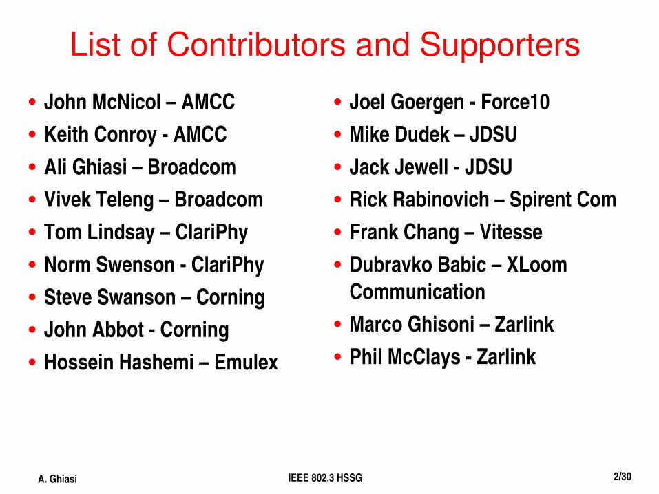
List of Contributors and Supporters
• John McNicol – AMCC• Keith Conroy AMCC• Ali Ghiasi – Broadcom• Vivek Teleng – Broadcom• Tom Lindsay – ClariPhy• Norm Swenson ClariPhy• Steve Swanson – Corning• John Abbot Corning• Hossein Hashemi – Emulex
• Joel Goergen Force10• Mike Dudek – JDSU• Jack Jewell JDSU• Rick Rabinovich – Spirent Com• Frank Chang – Vitesse• Dubravko Babic – XLoom
Communication• Marco Ghisoni – Zarlink• Phil McClays Zarlink

IEEE 802.3 HSSG3
A. Ghiasi 3/30
Overview
• The current assumption is not to use CDR in the 4x and 10x modules due to power dissipation and added cost.
• SFI single lane limiting specifications will be too difficult for 4x and 10x links.
• TX preemphasis and EDC either adaptive or nonadaptive will be used for all implementations to overcome FR4 losses.
• Limiting module specifications would be difficult to close even if the fibre reach is reduced from 300 m to 100 m on OM3 due to transmit DDJ.
• Linear module specifications with adaptive EDC provides extra margin to close the link without using CDR in the module.
• Propose SLI as the electrical interface which is light version of SFI.

IEEE 802.3 HSSG4
A. Ghiasi 4/30
PMA interface for the 4x10G
• SFI chips early on can enable the market.
4 x SFI,
QSFP
4 x SLI
MACReconciliation
PCS (APL/CTBI?)
Upper Layer Protocols
Multilane PMDMDI
Medium
PMD PMD PMD PMD

IEEE 802.3 HSSG5
A. Ghiasi 5/30
PMA interface for the 4x25G
• Same interface can support 10x10G
4 x SFI,
4x25GOptical XCVR
4 x SLI
MACReconciliation
PCS (APL/CTBI?)
Upper Layer Protocols
Multilane PMDMDI
Medium
PMD PMD PMD PMD
10:4 Mux/DeMux
PCS PCS PCS PCS
Ali Ghiasi

IEEE 802.3 HSSG6
A. Ghiasi 6/30
Block Diagram Limiting and Linear SFI/SLI
• Limiting SFI/SLI SFP + Connector (20 Positions)
SFI/SLI Channel
SFP + Module
Laser
LD DriverTP2
Limiter
PD/TIATP3
SFP + Connector (20 Positions)
SFI/SLI Channel
Laser
LD DriverTP2
AGC*
PD/TIATP3
• Linear SFI/SLI
* Common implementation incorporates AGC in the PD/TIA
B
C'D
B'
C SFP + Module
Host /SerDes
PreEmphasis
Mux
DeMux
Non Adaptive
EDC
Host /SerDes
PreEmphasis
Mux
DeMux
AdaptiveEDC
TX
RX
TX
RX
A

IEEE 802.3 HSSG7
A. Ghiasi 7/30
The Benefit of Linear Module Interface with Adaptive EDC
• EDC allow using slower lasers and detectors• Allow longer fibre reach • Support longer FR4 PCB traces• No need for the CDR in the module
– Enable smaller form factor– Lower power dissipation
• Lower cost• Potentially common host chips with the backplane and copper
cable.

8IEEE 802.3 HSSG
8A. Ghiasi 8/30
4X/10X Jitter Degradation Starting with SFI
• SFI DDJ at B=0.1 UI– DDJ at Host Output ( B ) for 4x link is expect at least 0.15 UI– DDJ at Host Output ( B ) for 10x link is expected to be at least 0.18
Degradation 4x Jitter (UI) 10x (UI)SFI B 0.100 0.100SerDes Penalty 0.025 0.040PCB Routing 0.025 0.040Total DDJ B 0.150 0.180Total TJ B 0.320 0.360
Degradation 4x Jitter (UI) 10x (UI)SFI C' 0.7 0.7SerDes Penalty 0.04 0.07PCB Routing 0.02 0.03TJ at C' 0.64 0.6

IEEE 802.3 HSSG9
A. Ghiasi 9/30
Starting Limiting Jitter Budget• Assumption made
– 10x10 Gig optics is given no excess penalty– DJ would increase by 0.05 UI
Jitter Compliance Points Β TP2 Fiber TP3 C*
4x10Gig
DJ UI 0.150 0.300 0.050 0.350 0.450
TJ UI 0.320 0.500 0.550 0.715
1-sigma RJ at max DJ for BER 1E-12 (ps) 1.178 1.386 1.386 1.836
10x10 Gig
DJ UI 0.180 0.330 0.050 0.380 0.480
TJ UI 0.360 0.550 0.600 0.765
1-sigma RJ at max DJ for BER 1E-12 (ps) 1.247 1.524 1.524 1.975
IEEE 802.3 HSSG10
A. Ghiasi 10/30
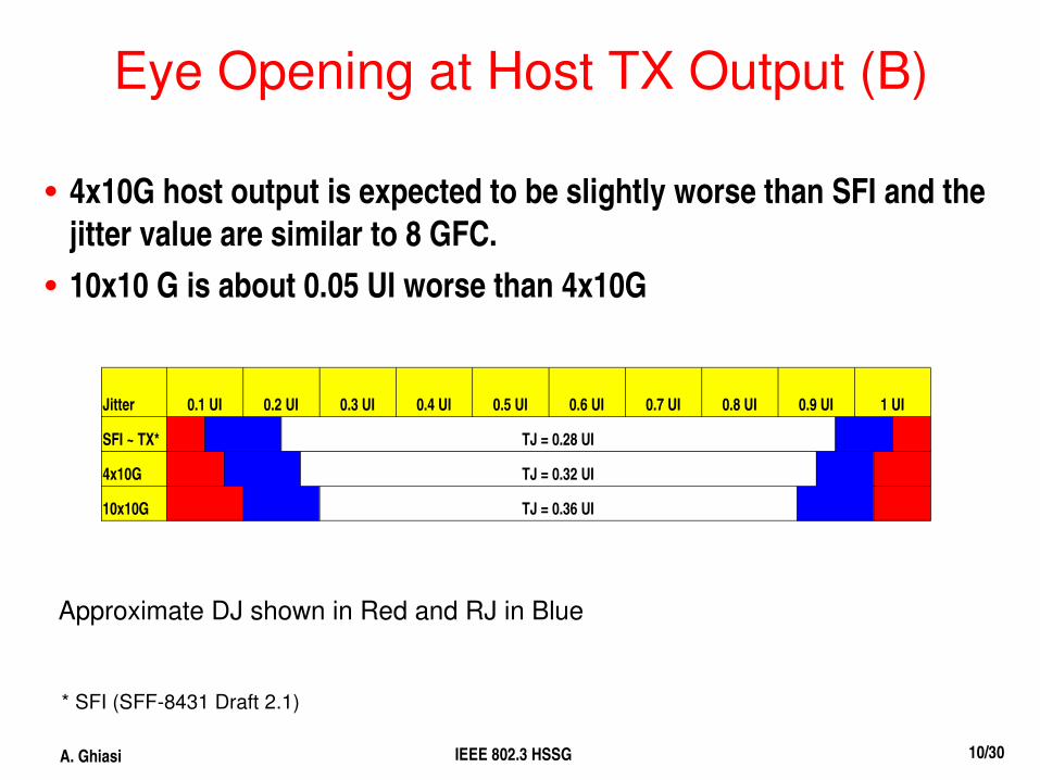
Eye Opening at Host TX Output (B)
• 4x10G host output is expected to be slightly worse than SFI and the jitter value are similar to 8 GFC.
• 10x10 G is about 0.05 UI worse than 4x10G
Jitter 0.1 UI 0.2 UI 0.3 UI 0.4 UI 0.5 UI 0.6 UI 0.7 UI 0.8 UI 0.9 UI 1 UI
SFI ~ TX* TJ = 0.28 UI
4x10G TJ = 0.32 UI
10x10G TJ = 0.36 UI
Approximate DJ shown in Red and RJ in Blue
* SFI (SFF8431 Draft 2.1)

IEEE 802.3 HSSG11
A. Ghiasi 11/30
Eye Opening at Host RX Input (C)
Jitter 0.1 UI 0.2 UI 0.3 UI 0.4 UI 0.5 UI 0.6 UI 0.7 UI 0.8 UI 0.9 UI 1 UI
SFI * TJ = 0.7 UI
4x10G TJ = 0.715 UI
10x10G TJ = 0.765 UI
4x SerDesTJ Input Max=0.64 UI
10x SerDesTJ Input Max=0.6 UI
Approximate DJ shown in Red and RJ in Blue
• 4x and 10x Jitter budget can not be closed reliably for limiting interface
When the module output TJ exceed the SerDes maximum input jitter the link does not close:
• The option is to use a linear receiver with lower overall cost and power
* SFI (SFF8431 Draft 2.1)

12IEEE 802.3 HSSG
12A. Ghiasi 12/30
SFI TP2 Simulation Setup
SFP + Connector (20 Positions)
TX
Noise
Soft LimiterTP2 OutputBT4
TX – Tr 47 ps
Transmitter
Host ASIC/SerDes
Mux + PreEmphasis
SFIChannel2”, 6”, 12”
• RIN penalty is not included• 2 inch stripline channel was inserted• Noise source at the SerDes was adjusted for UJ of ~0.023 UI (RMS) at B.• BT4 filter in the module was adjusted for Trise/fall of 47 ps 2080%.• Results shown is for optimum preemphasis

13IEEE 802.3 HSSG
13A. Ghiasi 13/30
SFI Transmitter Output with Optimum Preemphasis
2” Fr413 6” Fr413 12” Fr413
• Preemphasis single TSpaced post– Eye mask will get degraded further due to PCB and IC variations!

14IEEE 802.3 HSSG
14A. Ghiasi 14/30
Eye Diagram for 3 Sub10G Transmitters
SupplierA
• aronson_01_0907.pdf stated parallel link need more margin so we started with 3 sub10G transmitters
– The lasers DJ and TJ are similar to the jitter spreadsheet on page 9 at TP2!
DJ=32.3 psTJ=48.7 psDDJ=32.3 psDDPWS=20 ps
DJ=31.4 psTJ=46.5 psDDJ=31.4 psDDPWS=19.7 ps
DJ=41.6 psTJ=57.3 psDDJ=44.3 psDDPWS=19.1 ps
SupplierB SupplierC

15IEEE 802.3 HSSG
15A. Ghiasi 15/30
Impulse for 3 Sub10G Transmitters
• All 3 lasers exhibit strong precursor
SupplierA SupplierB SupplierC
16IEEE 802.3 HSSG
16A. Ghiasi 16/30
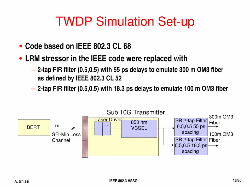
TWDP Simulation Setup
TX
Laser Driver 850 nmVCSEL
Sub 10G Transmitter
BERT SFIMin LossChannel SR 2tap Filter
0.5,0.5 18.3 ps spacing
100m OM3Fiber
SR 2tap Filter0.5,0.5 55 ps
spacing
300m OM3Fiber
• Code based on IEEE 802.3 CL 68• LRM stressor in the IEEE code were replaced with
– 2tap FIR filter (0.5,0.5) with 55 ps delays to emulate 300 m OM3 fiber as defined by IEEE 802.3 CL 52
– 2tap FIR filter (0.5,0.5) with 18.3 ps delays to emulate 100 m OM3 fiber

17IEEE 802.3 HSSG
17A. Ghiasi 17/30
TWDP Penalty as Function of FFE and DFE Taps (no fibre stressor)
• Based on the study of 3 suppliers A, B, and C sub 10G transmitters– Fiber and the RX electrical PCB/connector not included – Min reference receiver would be 4 T/2 FFE+2 T DFE
1 2 3 4 5 6 7 8 9 10 11 12 13 142.5
2.75
3
3.25
3.5
3.75
4
4.25
4.5
4.75
A2DFE
B2DFE
C2DFE
A3DFE
B3DFE
C3DFE
A4DFE
B4DFE
C4DFE
# FFE Tap
TW
DP
Pen
alty
(dB
o)

18IEEE 802.3 HSSG
18A. Ghiasi 18/30
WDP Penalty as Function of FFE and DFE Taps for 100m and 300
• Transmitter A response with 100m and 300 m of OM3 fiber– RX electrical PCB/connector not included – Reference receiver with 4 T/2 FFE+2 T DFE should be sufficient for 100m– Reference Receiver with 6 T/2 FFE+ 2 T DFE should be sufficient for 300m
1 2 3 4 5 6 7 82.5
3
3.5
4
4.5
5
5.5
6
6.5
7
0DFE100m
0DFE300m
2DFE100m
2DFE300m
3DFE100m
3DFE300m
4DFE100m
4DFE300m
# FFE Tap
TWD
P P
enal
ty (
dBo)

IEEE 802.3 HSSG19
A. Ghiasi 19/30
Relative Power of the Host Receivers• The limiting interface due to FR4 traces and connector require ~2 tap DFE+CDR.
• The linear interface require 4 to 6 tap T/2 FFE + 2 to 3 tap DFE+CDR.
• Increasing the limiting receiver EQ taps to support linear has overall cost and power advantage over putting a 2nd CDR in the module!
130 nm 65 nm 45 nm0
10
20
30
40
50
60
70
80
90
100
CDR
2DFE
6FFE2DFE
Process
Rel
ativ
e P
ower
%

IEEE 802.3 HSSG20
A. Ghiasi 20/30
Compatibility Requirement Between Limiting and Linear Interfaces
• Propose use of linear and limiting module – All modules with a mux will be limiting– All modules with 10G baudrate and without a mux will be linear.– A limiting module can plug in to a linear host
Solution Link Bit Rate Elec Elec Symbol Limiting Linear Retime Compatible
(Gb/s) Lanes Rate (Gbaud) Module Module Module with Adp EDC Host
XFP 10 1 10 x x x
SFP+ (Limiting) 10 1 10 x x
SFP+ (Linear) 10 1 10 x x
4x10G (SR) 40 4 10 x x
10x10G (SR) 100 10 10 x x
4x25G Gen 1 100 10 10 x x x
4x25G Gen 2 100 4 25 x x TBD

21IEEE 802.3 HSSG
21A. Ghiasi 21/30
Conclusion• SFI limiting jitter specifications are very challenging and would be
very difficult to scale to 4x and 10x limiting link.• Use of linear interface with adaptive EDC can allow
– Relaxing SerDes transmitter– Relaxing SerDes receiver– Allowing more margin for the host implementations– Common electrical interface for 4x and 10x– Use lower cost optics.– Possible SerDes chip commonality with copper cable and backplane.
• Linear can do 300 m with about 1 dB less penalty than limiting can do 100 m!
22IEEE 802.3 HSSG
22A. Ghiasi 22/30
Reference Material/Back Up Material
• For detail description of linear and limiting interface see: “Nextgeneration 10 GBaud module based on emerging SFP+ with hostbased EDC”, IEEE Communications Magazine, vol. 45, no. 3, March2007, pp. 32 38
• DDJ – Data Dependent Jitter
• DDWPS – Data Dependent Pulse Width Shrinkage
• TDP – Transmitter Dispersion Penalty see IEEE 802.3 CL 52
• TWDP – Transmitter Waveform Dispersion Penalty see IEEE 802.3 CL68
• WDP – Waveform Dispersion Penalty see SFF8431 ftp://ftp.seagate.com/sff/SFF8431.PDF

23IEEE 802.3 HSSG
23A. Ghiasi 23/30
SFI Reference Channels
• 5 mils Stripline channels with 2”, 6”, 8”, and 12” length– Traces include 2 via stubs– Include the PT enhanced connector (XFP, SFP+)– s4p files provided by Broadcom are available for the striplines and a set of microstrip
channels from www.t11.org doc # T11 06683v0

24IEEE 802.3 HSSG
24A. Ghiasi 24/30
SFI Reference Channels
• 12 mils Microstrip channels with 2”, 6”, 8”, and 12” length– Include the PT enhanced connector (XFP, SFP+)– s4p files provided by Broadcom are available for the striplines and a set of microstrip
channels from www.t11.org doc # T11 06683v0

25IEEE 802.3 HSSG
25A. Ghiasi 25/30
Informative Return Loss for Host and SFP+ Chips for 1011Gig
• More relax than XFI and similar to OIF CEI– Based on distributed models– Host chip 06236v0 and SFP+ chip is 06237v0 can be downloaded from T11 website.
Host Chip Return Loss SFP+ Chip Return Loss

26IEEE 802.3 HSSG
26A. Ghiasi 26/30
End to End Path Stripline
• Channel Response cascaded with the host IC and the module IC termination model T11 06236v0 and 06237v0

27IEEE 802.3 HSSG
27A. Ghiasi 27/30
End to End Path Microstrip
• Channel Response cascaded with the host IC and the module IC termination model T11 06236v0 and 06237v0

IEEE 802.3 HSSG28
A. Ghiasi 28/30
Channel End to End Impulse Response
• Each UI=97 ps

IEEE 802.3 HSSG29
A. Ghiasi 29/30
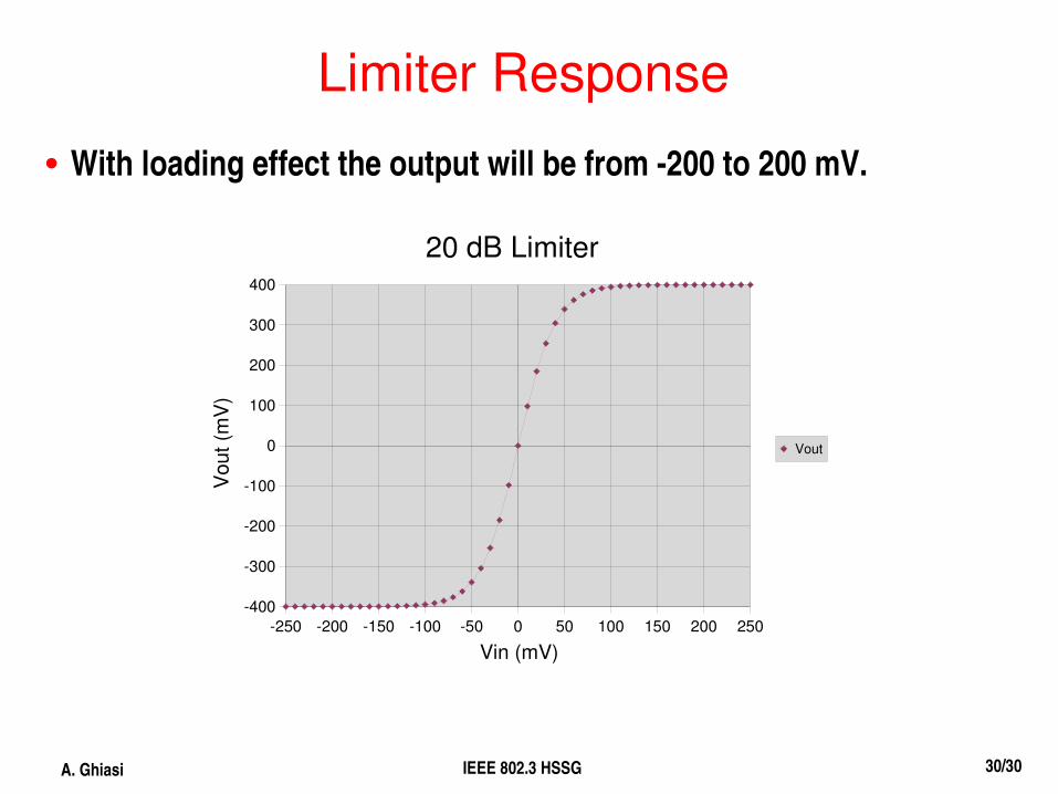
Transmitter/Limiter Model
• Limiter based on Hyperbolic Tangent– Soft limiter with 20 dB gain to emulate laser driver
• G=10 is the limiter Gain• Vs=400 is the saturated output level• Vi from 250 to 250 mV
• Laser is modelled currently as 47 ps rise time
Vo= Vi− [Vsx tanh G∗Vi /Vs ]
IEEE 802.3 HSSG30
A. Ghiasi 30/30
Limiter Response
• With loading effect the output will be from 200 to 200 mV.
250 200 150 100 50 0 50 100 150 200 250400
300
200
100
0
100
200
300
400
20 dB Limiter
Vout
Vin (mV)
Vou
t (m
V)