A Low-Power 9-bit Pipelined CMOS ADC for the front-end electronics of the Silicon Tracking System
Comparative Analysis of CMOS ADC
Topologies and Design of 4-Bit SAR ADC Using
Deep-submicron Technology
Kiran P. Kokate1, Amruta P. Chaudhary
2
1ME. student, G.H. Raisoni College of Engineering & Management, Amravati, (M.S.) India.
2Assistant Professor, PRMIT&R, Badnera,Amravati(M.S.), India
[email protected], [email protected]
Abstract: Analog-to-digital converters (ADCs) are key design blocks in digital systems and are currently used by
many application fields to improve digital systems, which achieve superior performances with respect to many
parameters. This paper presents the comparative analysis of different types of ADC based on different performance
parameters and design of SAR ADC. The application of ADC can be found in data acquisition systems, measurement
systems and digital communication systems. This paper provides comparison between different performance
parameters for ADCs & analyzing the better results & performance in future, the design of SAR ADC is suitable for
low power consumption. In modern era, VLSI design is one of the technique to have high speed, less power
consumption, effective use of space, easily available productivity and mobility. With the fast advancement of CMOS
technology, more & more signal processing functions are implemented in the digital domain for low cost, low power
consumption, higher yield, & higher reconfigurability.
Keywords: Analog to Digital Converter, CMOS, SAR, Low Power Consumption.
1 Introduction An Analog-to-Digital Converter (ADC),which is
used in digital system is a device that converts a
continuous physical quantity (usually voltage) to a
digital number which is the quantity's amplitude. The
conversion involves quantization of the input. Instead
of doing a single conversion, an ADC often performs
the conversions periodically. The result is a sequence
of digital values that have converted a continuous-
time and continuous-amplitude analog signal to a
discrete-time and discrete-amplitude digital signal.
ADC performs like a bridge between analog and
digital world.
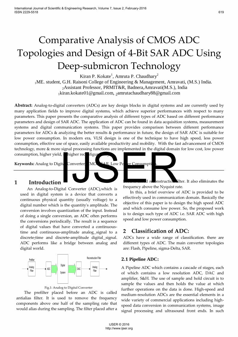
Fig.1: Analog to Digital Converter
The prefilter placed before an ADC is called
antialias filter. It is used to remove the frequency
components above one half of the sampling rate that
would alias during the sampling. The filter placed after a
DAC is called reconstruction filter. It also eliminates the
frequency above the Nyquist rate.
In this, a brief overview of ADC is provided to be
effectively used in communication domain. Basically the
objective of this paper is to design the high speed ADC
and which consume low power. So, the proposed work
is to design such type of ADC i.e. SAR ADC with high
speed and low power consumption.
2 Classification of ADC: ADCs have a wide range of classification. there are
different types of ADC. The main converter topologies
are: Flash, Pipeline, sigma-Delta, SAR.
2.1 Pipeline ADC:
A Pipeline ADC which contains a cascade of stages, each
of which contains a low resolution ADC, DAC and
amplifier, S&H. The use of sample and hold circuit is to
sample the values and then holds the value at which
further operations on the data is done. High-speed and
medium-resolution ADCs are the essential elements in a
wide variety of commercial applications including high-
speed data conversion in communication systems, image
signal processing and ultrasound front ends. In such
International Journal of Scientific & Engineering Research, Volume 7, Issue 2, February-2016 ISSN 2229-5518 619
IJSER © 2016 http://www.ijser.org
IJSER
applications, the reduction of power consumption
associated with high-speed sampling and quantization is
one key design issue to enhance portability and battery
operation of the system.
Fig.2: Pipeline ADC
2.2 Sigma-Delta (Σ - Δ) ADC:
Sigma-Delta converters are also called as oversampling
converters or charge balancing ADCs. Σ - Δ ADC sample
the input signals at a much higher rate than the
maximum input frequency. These converters are
classified as ADC topology that provides highest
resolution while still achieving high speed on the order of
24 bits at 1.5MHz. Oversampling & Noise shaping are the
two key techniques employed in these ADCs.
Oversampling helps avoid aliasing, improves resolution
and reduces noise. The sigma delta ADC oversamples the
desired signal by a large factor & filters the desired signal
band.
Fig.3: Sigma-Delta ADC
2.3 Flash ADC:
Flash ADC is highest speed of ADC, also called as
parallel ADC. Flash ADC uses one comparator per
quantization level (2N-1) and 2N resistors. The reference
voltage is divided into 2N values, each of which is fed
into comparator. The input voltage is compared with
each reference value and results in a thermometer code at
the output of the comparators. The value of thermometer
code remain all zero for each resistor level if the value of
VIN less than the value of resistor string and ones if the
value VIN is greater than the value of string.
Fig.4: Flash ADC
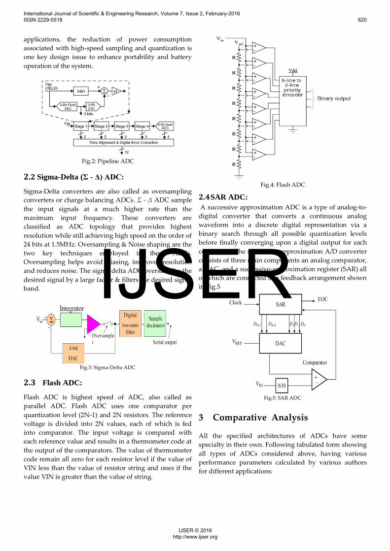
2.4 SAR ADC: A successive approximation ADC is a type of analog-to-
digital converter that converts a continuous analog
waveform into a discrete digital representation via a
binary search through all possible quantization levels
before finally converging upon a digital output for each
conversion. The successive-approximation A/D converter
consists of three main components an analog comparator,
a DAC, and a successive-approximation register (SAR) all
of which are connected in a feedback arrangement shown
in Fig.5
Fig.5: SAR ADC
3 Comparative Analysis
All the specified architectures of ADCs have some
specialty in their own. Following tabulated form showing
all types of ADCs considered above, having various
performance parameters calculated by various authors
for different applications:
International Journal of Scientific & Engineering Research, Volume 7, Issue 2, February-2016 ISSN 2229-5518 620
IJSER © 2016 http://www.ijser.org
IJSER
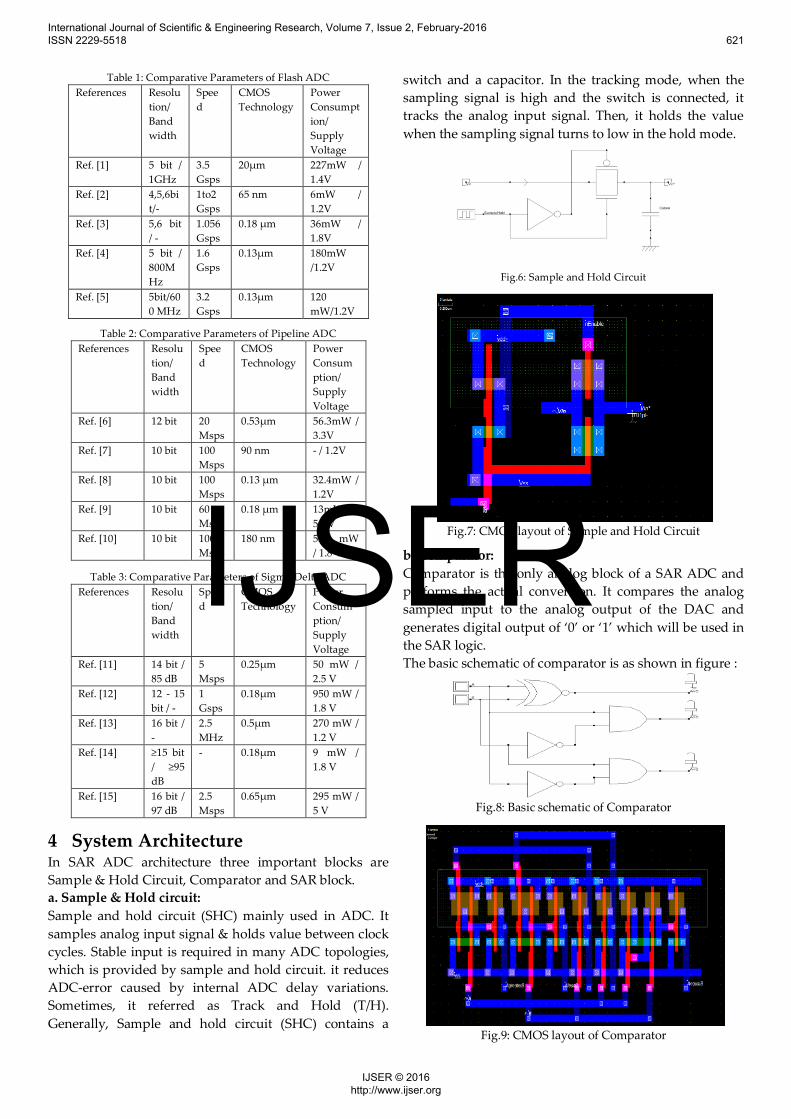
Table 1: Comparative Parameters of Flash ADC
References Resolu
tion/
Band
width
Spee
d
CMOS
Technology
Power
Consumpt
ion/
Supply
Voltage
Ref. [1] 5 bit /
1GHz
3.5
Gsps
20μm 227mW /
1.4V
Ref. [2] 4,5,6bi
t/-
1to2
Gsps
65 nm 6mW /
1.2V
Ref. [3] 5,6 bit
/ -
1.056
Gsps
0.18 μm 36mW /
1.8V
Ref. [4] 5 bit /
800M
Hz
1.6
Gsps
0.13μm 180mW
/1.2V
Ref. [5] 5bit/60
0 MHz
3.2
Gsps
0.13μm 120
mW/1.2V
Table 2: Comparative Parameters of Pipeline ADC References Resolu
tion/
Band
width
Spee
d
CMOS
Technology
Power
Consum
ption/
Supply
Voltage
Ref. [6] 12 bit 20
Msps
0.53μm 56.3mW /
3.3V
Ref. [7] 10 bit 100
Msps
90 nm - / 1.2V
Ref. [8] 10 bit 100
Msps
0.13 μm 32.4mW /
1.2V
Ref. [9] 10 bit 60
Msps
0.18 μm 13mW /
5mV
Ref. [10] 10 bit 100
Msps
180 nm 52.6 mW
/ 1.8 V
Table 3: Comparative Parameters of Sigma-Delta ADC References Resolu
tion/
Band
width
Spee
d
CMOS
Technology
Power
Consum
ption/
Supply
Voltage
Ref. [11] 14 bit /
85 dB
5
Msps
0.25μm 50 mW /
2.5 V
Ref. [12] 12 - 15
bit / -
1
Gsps
0.18μm 950 mW /
1.8 V
Ref. [13] 16 bit /
-
2.5
MHz
0.5μm 270 mW /
1.2 V
Ref. [14] ≥15 bit
/ ≥95
dB
- 0.18μm 9 mW /
1.8 V
Ref. [15] 16 bit /
97 dB
2.5
Msps
0.65μm 295 mW /
5 V
4 System Architecture In SAR ADC architecture three important blocks are
Sample & Hold Circuit, Comparator and SAR block.
a. Sample & Hold circuit:
Sample and hold circuit (SHC) mainly used in ADC. It
samples analog input signal & holds value between clock
cycles. Stable input is required in many ADC topologies,
which is provided by sample and hold circuit. it reduces
ADC-error caused by internal ADC delay variations.
Sometimes, it referred as Track and Hold (T/H).
Generally, Sample and hold circuit (SHC) contains a
switch and a capacitor. In the tracking mode, when the
sampling signal is high and the switch is connected, it
tracks the analog input signal. Then, it holds the value
when the sampling signal turns to low in the hold mode.
Fig.6: Sample and Hold Circuit
Fig.7: CMOS layout of Sample and Hold Circuit
b. Comparator:
Comparator is the only analog block of a SAR ADC and
performs the actual conversion. It compares the analog
sampled input to the analog output of the DAC and
generates digital output of ‘0’ or ‘1’ which will be used in
the SAR logic.
The basic schematic of comparator is as shown in figure :
Fig.8: Basic schematic of Comparator
Fig.9: CMOS layout of Comparator
International Journal of Scientific & Engineering Research, Volume 7, Issue 2, February-2016 ISSN 2229-5518 621
IJSER © 2016 http://www.ijser.org
IJSER
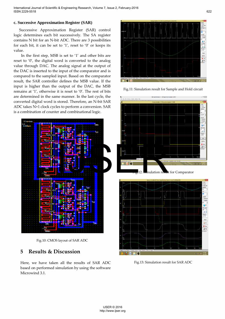
c. Successive Approximation Register (SAR)
Successive Approximation Register (SAR) control
logic determines each bit successively. The SA register
contains N bit for an N-bit ADC. There are 3 possibilities
for each bit, it can be set to ‘1’, reset to ‘0’ or keeps its
value.
In the first step, MSB is set to ‘1’ and other bits are
reset to ‘0’, the digital word is converted to the analog
value through DAC. The analog signal at the output of
the DAC is inserted to the input of the comparator and is
compared to the sampled input. Based on the comparator
result, the SAR controller defines the MSB value. If the
input is higher than the output of the DAC, the MSB
remains at ‘1’, otherwise it is reset to ‘0’. The rest of bits
are determined in the same manner. In the last cycle, the
converted digital word is stored. Therefore, an N-bit SAR
ADC takes N+1 clock cycles to perform a conversion. SAR
is a combination of counter and combinational logic.
Fig.10: CMOS layout of SAR ADC
5 Results & Discussion
Here, we have taken all the results of SAR ADC
based on performed simulation by using the software
Microwind 3.1.
Fig.11: Simulation result for Sample and Hold circuit
Fig.12: Simulation result for Comparator
Fig.13: Simulation result for SAR ADC
International Journal of Scientific & Engineering Research, Volume 7, Issue 2, February-2016 ISSN 2229-5518 622
IJSER © 2016 http://www.ijser.org
IJSER
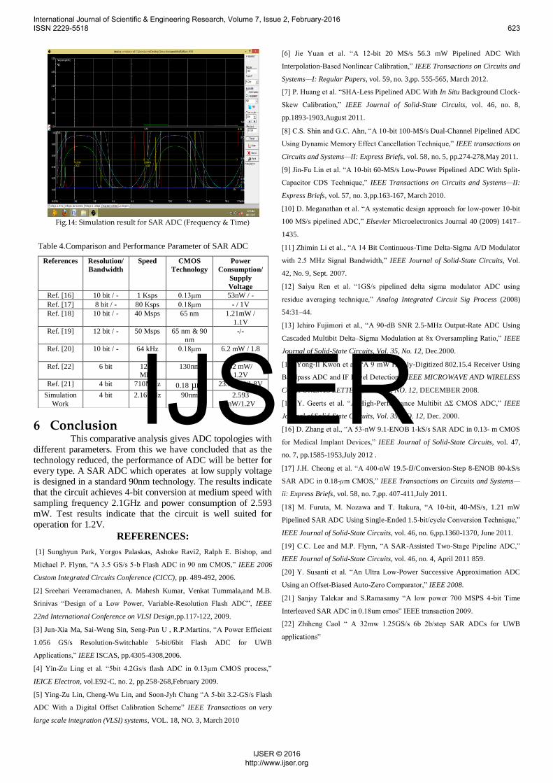
Fig.14: Simulation result for SAR ADC (Frequency & Time)
Table 4.Comparison and Performance Parameter of SAR ADC
References Resolution/
Bandwidth
Speed CMOS
Technology
Power
Consumption/
Supply
Voltage
Ref. [16] 10 bit / - 1 Ksps 0.13μm 53nW / -
Ref. [17] 8 bit / - 80 Ksps 0.18μm - / 1V
Ref. [18] 10 bit / - 40 Msps 65 nm 1.21mW /
1.1V
Ref. [19] 12 bit / - 50 Msps 65 nm & 90
nm
-/-
Ref. [20] 10 bit / - 64 kHz 0.18μm 6.2 mW / 1.8
V
Ref. [22] 6 bit 1250
MHz
130nm 32 mW/
1.2V
Ref. [21] 4 bit 710MHz 0.18 µm 23.3 mW/1.8V
Simulation
Work
4 bit 2.16GHz 90nm 2.593
mW/1.2V
6 Conclusion This comparative analysis gives ADC topologies with
different parameters. From this we have concluded that as the
technology reduced, the performance of ADC will be better for
every type. A SAR ADC which operates at low supply voltage
is designed in a standard 90nm technology. The results indicate
that the circuit achieves 4-bit conversion at medium speed with
sampling frequency 2.1GHz and power consumption of 2.593
mW. Test results indicate that the circuit is well suited for
operation for 1.2V.
REFERENCES:
[1] Sunghyun Park, Yorgos Palaskas, Ashoke Ravi2, Ralph E. Bishop, and
Michael P. Flynn, “A 3.5 GS/s 5-b Flash ADC in 90 nm CMOS,” IEEE 2006
Custom Integrated Circuits Conference (CICC), pp. 489-492, 2006.
[2] Sreehari Veeramachanen, A. Mahesh Kumar, Venkat Tummala,and M.B.
Srinivas “Design of a Low Power, Variable-Resolution Flash ADC”, IEEE
22nd International Conference on VLSI Design,pp.117-122, 2009.
[3] Jun-Xia Ma, Sai-Weng Sin, Seng-Pan U , R.P.Martins, “A Power Efficient
1.056 GS/s Resolution-Switchable 5-bit/6bit Flash ADC for UWB
Applications,” IEEE ISCAS, pp.4305-4308,2006.
[4] Yin-Zu Ling et al. “5bit 4.2Gs/s flash ADC in 0.13μm CMOS process,”
IEICE Electron, vol.E92-C, no. 2, pp.258-268,February 2009.
[5] Ying-Zu Lin, Cheng-Wu Lin, and Soon-Jyh Chang “A 5-bit 3.2-GS/s Flash
ADC With a Digital Offset Calibration Scheme” IEEE Transactions on very
large scale integration (VLSI) systems, VOL. 18, NO. 3, March 2010
[6] Jie Yuan et al. “A 12-bit 20 MS/s 56.3 mW Pipelined ADC With
Interpolation-Based Nonlinear Calibration,” IEEE Transactions on Circuits and
Systems—I: Regular Papers, vol. 59, no. 3,pp. 555-565, March 2012.
[7] P. Huang et al. “SHA-Less Pipelined ADC With In Situ Background Clock-
Skew Calibration,” IEEE Journal of Solid-State Circuits, vol. 46, no. 8,
pp.1893-1903,August 2011.
[8] C.S. Shin and G.C. Ahn, “A 10-bit 100-MS/s Dual-Channel Pipelined ADC
Using Dynamic Memory Effect Cancellation Technique,” IEEE transactions on
Circuits and Systems—II: Express Briefs, vol. 58, no. 5, pp.274-278,May 2011.
[9] Jin-Fu Lin et al. “A 10-bit 60-MS/s Low-Power Pipelined ADC With Split-
Capacitor CDS Technique,” IEEE Transactions on Circuits and Systems—II:
Express Briefs, vol. 57, no. 3,pp.163-167, March 2010.
[10] D. Meganathan et al. “A systematic design approach for low-power 10-bit
100 MS/s pipelined ADC,” Elsevier Microelectronics Journal 40 (2009) 1417–
1435.
[11] Zhimin Li et al., “A 14 Bit Continuous-Time Delta-Sigma A/D Modulator
with 2.5 MHz Signal Bandwidth,” IEEE Journal of Solid-State Circuits, Vol.
42, No. 9, Sept. 2007.
[12] Saiyu Ren et al. “1GS/s pipelined delta sigma modulator ADC using
residue averaging technique,” Analog Integrated Circuit Sig Process (2008)
54:31–44.
[13] Ichiro Fujimori et al., “A 90-dB SNR 2.5-MHz Output-Rate ADC Using
Cascaded Multibit Delta–Sigma Modulation at 8x Oversampling Ratio,” IEEE
Journal of Solid-State Circuits, Vol. 35, No. 12, Dec.2000.
[14] Yong-Il Kwon et al. “A 9 mW Highly-Digitized 802.15.4 Receiver Using
Bandpass ADC and IF Level Detection,” IEEE MICROWAVE AND WIRELESS
COMPONENTS LETTERS, VOL. 18, NO. 12, DECEMBER 2008.
[15] Y. Geerts et al. “A High-Performance Multibit ΔΣ CMOS ADC,” IEEE
Journal of Solid-State Circuits, Vol. 35, NO. 12, Dec. 2000.
[16] D. Zhang et al., “A 53-nW 9.1-ENOB 1-kS/s SAR ADC in 0.13- m CMOS
for Medical Implant Devices,” IEEE Journal of Solid-State Circuits, vol. 47,
no. 7, pp.1585-1953,July 2012 .
[17] J.H. Cheong et al. “A 400-nW 19.5-fJ/Conversion-Step 8-ENOB 80-kS/s
SAR ADC in 0.18-μm CMOS,” IEEE Transactions on Circuits and Systems—
ii: Express Briefs, vol. 58, no. 7,pp. 407-411,July 2011.
[18] M. Furuta, M. Nozawa and T. Itakura, “A 10-bit, 40-MS/s, 1.21 mW
Pipelined SAR ADC Using Single-Ended 1.5-bit/cycle Conversion Technique,”
IEEE Journal of Solid-State Circuits, vol. 46, no. 6,pp.1360-1370, June 2011.
[19] C.C. Lee and M.P. Flynn, “A SAR-Assisted Two-Stage Pipeline ADC,”
IEEE Journal of Solid-State Circuits, vol. 46, no. 4, April 2011 859.
[20] Y. Susanti et al. “An Ultra Low-Power Successive Approximation ADC
Using an Offset-Biased Auto-Zero Comparator,” IEEE 2008.
[21] Sanjay Talekar and S.Ramasamy “A low power 700 MSPS 4-bit Time
Interleaved SAR ADC in 0.18um cmos” IEEE transaction 2009.
[22] Zhiheng Caol “ A 32mw 1.25GS/s 6b 2b/step SAR ADCs for UWB
applications”
International Journal of Scientific & Engineering Research, Volume 7, Issue 2, February-2016 ISSN 2229-5518 623
IJSER © 2016 http://www.ijser.org
IJSER
International Journal of Scientific & Engineering Research, Volume 7, Issue 2, February-2016 ISSN 2229-5518 624
IJSER © 2016 http://www.ijser.org
IJSER