ColdFire+ Portfolio - Product Brief - NXP...
29
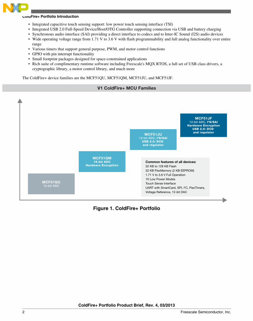
1 ColdFire+ Portfolio Introduction Freescale's ColdFire+ 32-bit microcontrollers are built on the Version 1 (V1) ColdFire® core and enabled by innovative 90 nm thin film storage (TFS) flash process technology with FlexMemory. The ColdFire+ portfolio consists of six families featuring ultra-low power capabilities in small footprint solutions with embedded flash memory that scales from 32 KB to 128 KB. The families offer a rich combination of additive peripherals including USB, high performance mixed signal capabilities, hardware encryption, an innovative touch sensing interface (TSI), and more. These key features make ColdFire+ microcontrollers ideal for portable handheld devices, wireless nodes, peripherals that require device authentication, building control security pads, and advanced remote control devices. The feature superset of all six pin- and software-compatible families includes: • Innovative FlexMemory enabling up to 2 KB of enhanced EEPROM or additional 32 KB of flash • 10 flexible low power modes, ideal for extending battery life • 16-bit or 12-bit ADC and 12-bit DAC to provide flexible and powerful mixed signal capabilities • Cryptographic Acceleration Unit (CAU) and Random Number Generator (RNGB) for secure communications Freescale Semiconductor Document Number:MCF51JxQxPB Product Brief Rev. 4, 03/2013 ColdFire+ Portfolio Product Brief Entry-level, 32-bit, ultra-low power, low cost, small form-factor, fully software- and pin-compatible solutions © 2010–2013 Freescale Semiconductor, Inc. Contents 1 ColdFire+ Portfolio Introduction...............................1 2 Target Applications...................................................3 3 Block Diagram..........................................................3 4 Features.....................................................................4 5 Developer Environment...........................................23 6 Revision History.....................................................28
Transcript of ColdFire+ Portfolio - Product Brief - NXP...
1 ColdFire+ PortfolioIntroduction
Freescale's ColdFire+ 32-bit microcontrollers are built on theVersion 1 (V1) ColdFire® core and enabled by innovative 90nm thin film storage (TFS) flash process technology withFlexMemory. The ColdFire+ portfolio consists of six familiesfeaturing ultra-low power capabilities in small footprintsolutions with embedded flash memory that scales from 32KB to 128 KB. The families offer a rich combination ofadditive peripherals including USB, high performance mixedsignal capabilities, hardware encryption, an innovative touchsensing interface (TSI), and more. These key features makeColdFire+ microcontrollers ideal for portable handhelddevices, wireless nodes, peripherals that require deviceauthentication, building control security pads, and advancedremote control devices.
The feature superset of all six pin- and software-compatiblefamilies includes:
• Innovative FlexMemory enabling up to 2 KB ofenhanced EEPROM or additional 32 KB of flash
• 10 flexible low power modes, ideal for extending batterylife
• 16-bit or 12-bit ADC and 12-bit DAC to provideflexible and powerful mixed signal capabilities
• Cryptographic Acceleration Unit (CAU) and RandomNumber Generator (RNGB) for secure communications
Freescale Semiconductor Document Number:MCF51JxQxPB
Product Brief Rev. 4, 03/2013
ColdFire+ Portfolio Product BriefEntry-level, 32-bit, ultra-low power, low cost, smallform-factor, fully software- and pin-compatiblesolutions
© 2010–2013 Freescale Semiconductor, Inc.
Contents
1 ColdFire+ Portfolio Introduction...............................1
2 Target Applications...................................................3
3 Block Diagram..........................................................3
4 Features.....................................................................4
5 Developer Environment...........................................23
6 Revision History.....................................................28
• Integrated capacitive touch sensing support: low power touch sensing interface (TSI)• Integrated USB 2.0 Full-Speed Device/Host/OTG Controller supporting connection via USB and battery charging• Synchronous audio interface (SAI) providing a direct interface to codecs and to Inter-IC Sound (I2S) audio devices• Wide operating voltage range from 1.71 V to 3.6 V with flash programmability and full analog functionality over entire
range• Various timers that support general purpose, PWM, and motor control functions• GPIO with pin interrupt functionality• Small footprint packages designed for space-constrained applications• Rich suite of complimentary runtime software including Freescale's MQX RTOS, a full set of USB class drivers, a
cryptographic library, a motor control library, and much more
The ColdFire+ device families are the MCF51QU, MCF51QM, MCF51JU, and MCF51JF.
Figure 1. ColdFire+ Portfolio
ColdFire+ Portfolio Introduction
ColdFire+ Portfolio Product Brief, Rev. 4, 03/2013
2 Freescale Semiconductor, Inc.
2 Target ApplicationsColdFire+ devices are optimal for a myriad of applications. The following table provides a partial list.
Table 1. Target Applications
Target application Description
Building, home, or industrial automation Electronic toll collection
Magnetic card reader
Wireless sensor/control nodes
Security/access control
HVAC control
Light automation
Portable consumer devices MP3 player accessories
Digital radio
Medical devices Portable medical devices
Mid-end/high-end PC peripheral accessories High-quality audio via USB
Full feature keyboard with touch pad, speakers, and microphone
Joysticks
General purpose applications High-end remote control
Metering/instrumentation
Video game accessories
3 Block DiagramThe block diagram shows the feature categories of all ColdFire+ device families, including those shared by and differingamong the families.
Target Applications
ColdFire+ Portfolio Product Brief, Rev. 4, 03/2013
Freescale Semiconductor, Inc. 3

Memory andMemory Interfaces
Flash RAM
12-bit DAC
6-bit DAC
CRC
Xtrinsic TouchSensing I/F
Analog Timers CommunicationInterfaces
System Securityand Integrity
SPI x2Carrier
ModulatorTransmitter
FlexNVM
ClocksCore and System
CPU Debug
AnalogComparator
VoltageReference
Low PowerTimers x2
Human-MachineInterface (HMI)
GPIO
PowerManagement
Watchdog
Frequency-Locked Loop
SerialProgrammingI/F (EzPort)
Phase-Locked Loop
InternalReference
Clocks
ProgrammableDelay Block
ModuloTimer
Low/HighFrequencyOscillators
UART x2 (withSmart Card)I2C x4Timers x2
ExternalInterrupt
Direct MemoryAccess
Low-LeakageWakeup
InterruptController
CrossbarSwitch
Only on QM & JFLEGEND Only on
QMOnly on QU,JU & JF
Only onJU & JF
V1 ColdFire Core
External BusInterface
(Mini-FlexBus)
FlexRAM
ColdFire+ Jx/Qx Families
USB ChargerDetect
VoltageRegulator
USB OTGLS/FS
I2S/SAI
RandomNumber
Generator
HardwareEncryption
(CAU)
16-bit ADC
12-bit ADC
EnhancedMultiply-
Accumulator
HardwareDivide
PowerManagement
Controller
System ModeController
Figure 2. Block Diagram of ColdFire+ Device Families
4 FeaturesThis section describes features of the entire ColdFire+ portfolio as well as of individual families, devices, and devicecomponents.
Features
ColdFire+ Portfolio Product Brief, Rev. 4, 03/2013
4 Freescale Semiconductor, Inc.
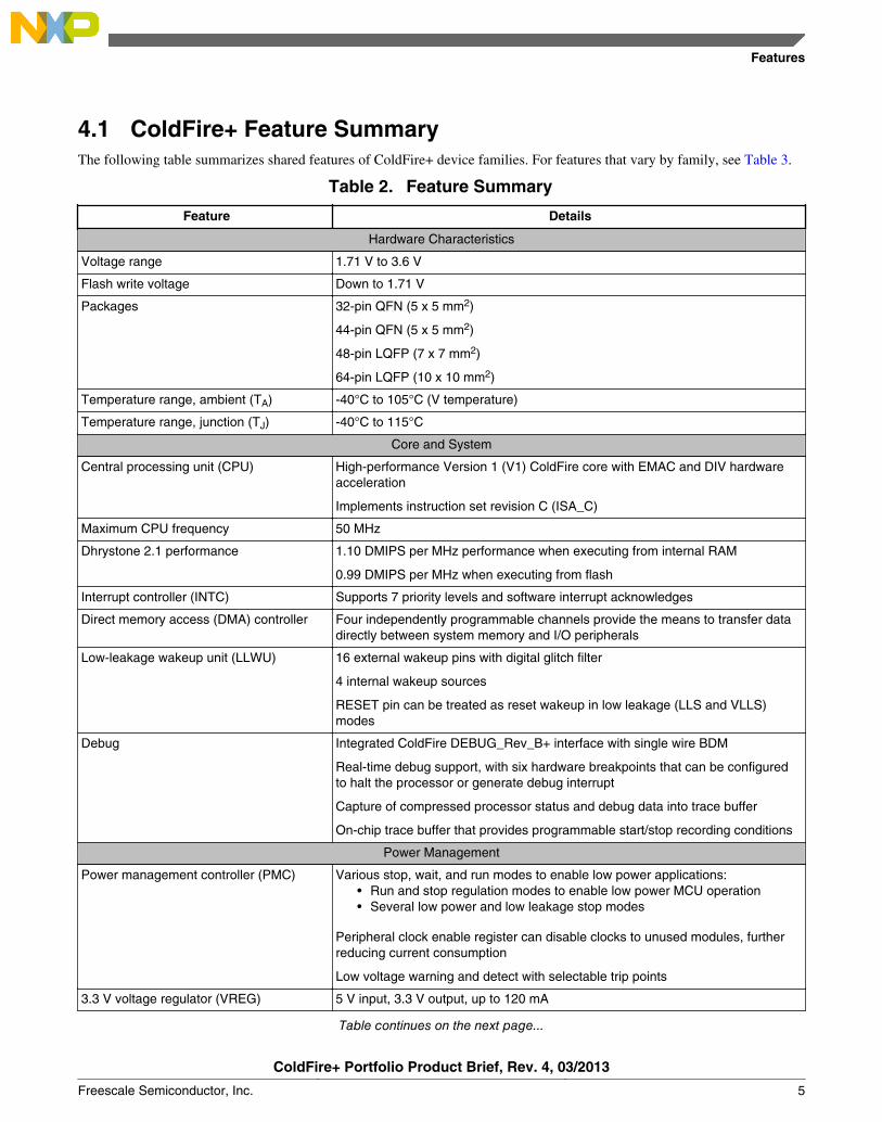
4.1 ColdFire+ Feature SummaryThe following table summarizes shared features of ColdFire+ device families. For features that vary by family, see Table 3.
Table 2. Feature Summary
Feature Details
Hardware Characteristics
Voltage range 1.71 V to 3.6 V
Flash write voltage Down to 1.71 V
Packages 32-pin QFN (5 x 5 mm2)
44-pin QFN (5 x 5 mm2)
48-pin LQFP (7 x 7 mm2)
64-pin LQFP (10 x 10 mm2)
Temperature range, ambient (TA) -40°C to 105°C (V temperature)
Temperature range, junction (TJ) -40°C to 115°C
Core and System
Central processing unit (CPU) High-performance Version 1 (V1) ColdFire core with EMAC and DIV hardwareacceleration
Implements instruction set revision C (ISA_C)
Maximum CPU frequency 50 MHz
Dhrystone 2.1 performance 1.10 DMIPS per MHz performance when executing from internal RAM
0.99 DMIPS per MHz when executing from flash
Interrupt controller (INTC) Supports 7 priority levels and software interrupt acknowledges
Direct memory access (DMA) controller Four independently programmable channels provide the means to transfer datadirectly between system memory and I/O peripherals
Low-leakage wakeup unit (LLWU) 16 external wakeup pins with digital glitch filter
4 internal wakeup sources
RESET pin can be treated as reset wakeup in low leakage (LLS and VLLS)modes
Debug Integrated ColdFire DEBUG_Rev_B+ interface with single wire BDM
Real-time debug support, with six hardware breakpoints that can be configuredto halt the processor or generate debug interrupt
Capture of compressed processor status and debug data into trace buffer
On-chip trace buffer that provides programmable start/stop recording conditions
Power Management
Power management controller (PMC) Various stop, wait, and run modes to enable low power applications:• Run and stop regulation modes to enable low power MCU operation• Several low power and low leakage stop modes
Peripheral clock enable register can disable clocks to unused modules, furtherreducing current consumption
Low voltage warning and detect with selectable trip points
3.3 V voltage regulator (VREG) 5 V input, 3.3 V output, up to 120 mA
Table continues on the next page...
Features
ColdFire+ Portfolio Product Brief, Rev. 4, 03/2013
Freescale Semiconductor, Inc. 5

Table 2. Feature Summary (continued)
Feature Details
Memory and Memory Interfaces
Total flash memory Up to 160 KB (128 KB + 32 KB)
Program flash Up to 128 KB
FlexNVM Up to 32 KB
FlexRAM Up to 2 KB
RAM Up to 32 KB
Total random access memory (RAM) Up to 34 KB (32 KB + 2 KB)
FlexMemory (FlexNVM plus FlexRAM)configuration examples1
Example 1: 32 KB additional program flash, no data flash or EEPROM, 2 KBadditional RAM
Example 2: 32 KB data flash memory, 2 KB additional RAM
Example 3: Up to 2 KB high-endurance, nonvolatile, enhanced EEPROM
Example 4: Partial data flash and EEPROM
Low-leakage standby memory Full RAM in LLS and VLLS3 power modes, 1 KB RAM or 8KB RAM in VLLS2mode
32-byte register file in all power modes, including VLLS1 mode
External bus interface (Mini-FlexBus) Supports glueless connections to external memories and peripherals
Up to 20 address and 8 data lines (non-muxed mode)
Up to 20 address lines and 16 data lines (muxed mode)
2 chip selects
Serial programming interface (EzPort) Supports flash in-system programming
Clocks
External crystal oscillator or resonator Low range, low power, or full-swing: 32 kHz to 40 kHz
Medium range, low power, or full-swing: 1 MHz to 8 MHz
High range, low power, or full-swing: 8 MHz to 32 MHz
External clock DC to 50 MHz
Internal clock references Two internal trimmable reference clocks• 32 kHz• 2 MHz
Internal 1 kHz low power oscillator
Phase-locked loop (PLL) Up to 100 MHz VCO
Frequency-locked loop (FLL) 1
System Security and Integrity
Cyclic redundancy check (CRC) module User configurable 16/32-bit hardware CRC generator circuit with programmablegenerator polynomial
Supports checksumming of any memory image
COP watchdog module 1
Memory Flash security features and block protection
Unique chip identification (ID) number 128 bits wide
Analog
Analog-to-digital converter (ADC) 1 successive approximation (SAR) ADC
Table continues on the next page...
Features
ColdFire+ Portfolio Product Brief, Rev. 4, 03/2013
6 Freescale Semiconductor, Inc.

Table 2. Feature Summary (continued)
Feature Details
12-bit digital-to-analog converter (DAC) 1
High-speed comparator (CMP) 1 with 6-bit DAC
Programmable voltage reference (VREF) 1
Timers
Programmable delay block (PDB) 1 ADC channel (with 2 triggers), 1 DAC channel, and 1 pulse-out to CMP
16-bit flexible timer (FTM0) Up to 2 channels, with quadrature decoder
16-bit flexible timer (FTM1) 6 channels
16-bit modulo timer (MTIM) 1
Carrier modulator transmitter (CMT) 1
Low-power timers (LPTMR0 and LPTMR1) Support Time of Day function with an external 32.768 kHz low power crystaloscillator
1-channel, 16-bit pulse counter or periodic interrupt
Communication Interfaces
16-bit serial peripheral interface (SPI0) 1 with independent 8-byte transmit and receive FIFOs
16-bit serial peripheral interface (SPI1) 1 (without FIFO)
Inter-Integrated Circuit (I2C) Up to 4
Universal asynchronous receivers/transmitters (UART0 and UART1)
Serial communications interface (SCI)
Support for ISO 7816 protocol for interfacing with smart cards
Hardware flow control
Higher baud rates (CPU clock)
Independent data FIFO for transmit and receive
Human-Machine Interface (HMI)
Rapid general-purpose input/output(RGPIO)2
Up to 16 bits of high-speed GPIO functionality connected to the processor's local32-bit bus with faster set, clear, and toggle functionality
Enhanced general-purpose input/output(EGPIO)
Up to 48
Pin interrupt / DMA request capability
Up to 16 EGPIOs (PORTB and PORTC) with digital glitch filter
Hysteresis and configurable pullup/pulldown device on all input pins
Configurable slew rate and drive strength on all output pins
Touch sensing inputs (TSI) Up to 16
Interrupt Request Pin (IRQ) Rising or falling edge selection
Level sensitivity option
Configurable internal pullup/pulldown
Defined as a nonmaskable interrupt request
1. FlexNVM can be used as program flash, as data flash, or, in conjunction with FlexRAM, as high-endurance EEPROM or acombination of data flash and EEPROM.
2. Shared with EGPIO pins
The following table summarizes features that vary by family.
Features
ColdFire+ Portfolio Product Brief, Rev. 4, 03/2013
Freescale Semiconductor, Inc. 7

Table 3. Feature Differences
QU QM JU JF Feature Details
System Security and Integrity
No Yes No Yes Random number generator (RNGB) Supports both true (TRNG) and pseudo-randomnumber (PRNG) generators
No Yes No Yes Cryptographic Acceleration Unit (CAU) Provides hardware encryption for:• DES• AES{-128, -192, -256}• SHA-1 and SHA-256• MD5
Enables more complex algorithms such as 3DES withsoftware encryption libraries that use the precedingbasic security blocks
Analog
No Yes No No 16-bit analog-to-digital converter (ADC) Up to 18 single-ended channels
Up to 2 differential channels (differential pairs)
Yes No Yes Yes 12-bit analog-to-digital converter (ADC) Up to 19 single-ended channels
Communication Interfaces
No No Yes Yes Universal Serial Bus (USB) 2.0 On-the-Go (OTG) controller1
Low-speed, full-speed
Host, device, and OTG support
No No Yes Yes USB device charger detect (DCD) Compliant with USB Battery Charging Specification,Revision 1.1, and supporting programmable timingparameters
No No Yes Yes Inter-IC Sound (I2S) / SynchronousAudio Interface (SAI)
1
1. The 3.3 V voltage regulator on all ColdFire+ devices powers the on-chip USB transceiver. The regulator input supports the5 V supply typically provided by USB VBUS power.
4.2 Features by PackageThe following summary identifies some aspects of common family features that vary by package. For a similar summary offeatures that vary by family and package, refer to Table 5.
Table 4. Feature Summary by Package
Part number
xx refers to every family:
JF, JU, QM, QU
MC
F51
xx32
VF
M
MC
F51
xx32
VH
S
MC
F51
xx64
VL
F
MC
F51
xx64
VH
S
MC
F51
xx12
8VH
S
MC
F51
xx12
8VL
H
Package type and number of pins 32-pin QFN 44-pin QFN48-pinLQFP
44-pin QFN64-pinLQFP
Package dimensions (mm x mm) 5x5 5x5 7x7 5x5 10x10
Core Processor
Table continues on the next page...
Features
ColdFire+ Portfolio Product Brief, Rev. 4, 03/2013
8 Freescale Semiconductor, Inc.
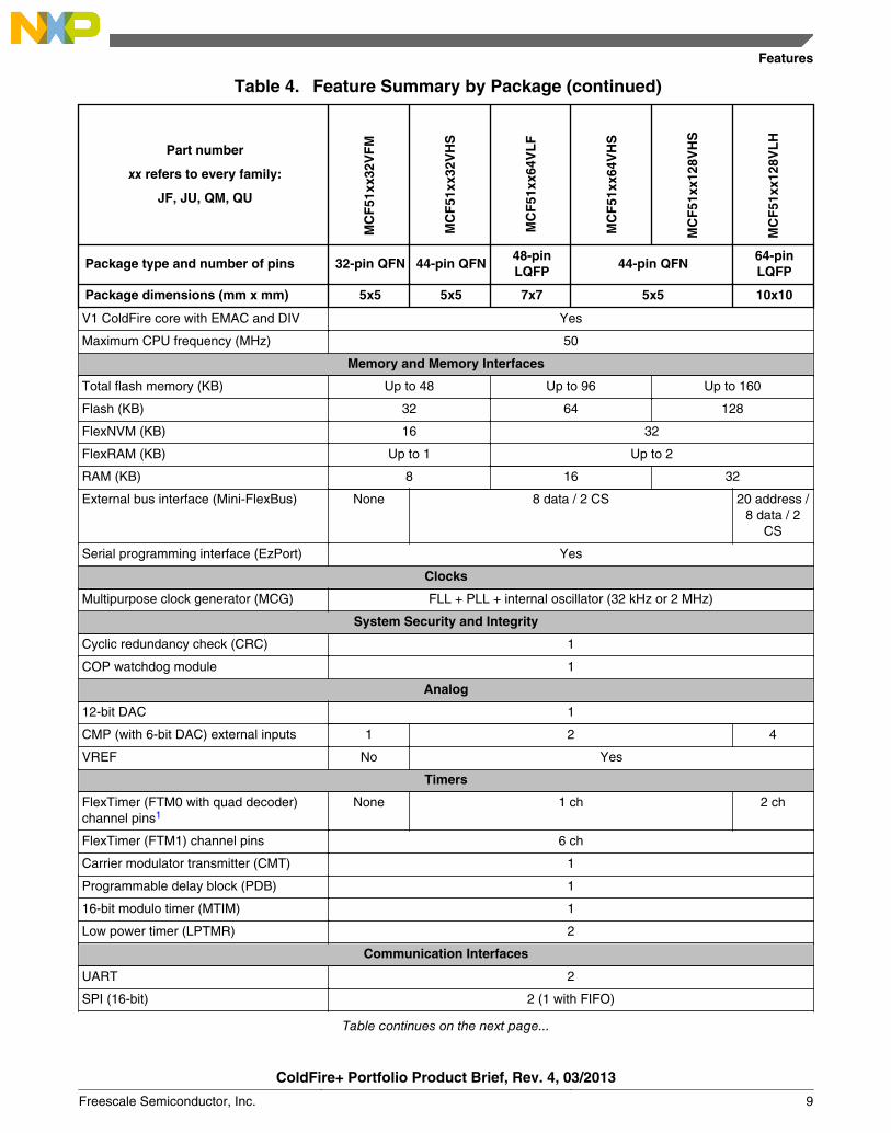
Table 4. Feature Summary by Package (continued)
Part number
xx refers to every family:
JF, JU, QM, QU
MC
F51
xx32
VF
M
MC
F51
xx32
VH
S
MC
F51
xx64
VL
F
MC
F51
xx64
VH
S
MC
F51
xx12
8VH
S
MC
F51
xx12
8VL
H
Package type and number of pins 32-pin QFN 44-pin QFN48-pinLQFP
44-pin QFN64-pinLQFP
Package dimensions (mm x mm) 5x5 5x5 7x7 5x5 10x10
V1 ColdFire core with EMAC and DIV Yes
Maximum CPU frequency (MHz) 50
Memory and Memory Interfaces
Total flash memory (KB) Up to 48 Up to 96 Up to 160
Flash (KB) 32 64 128
FlexNVM (KB) 16 32
FlexRAM (KB) Up to 1 Up to 2
RAM (KB) 8 16 32
External bus interface (Mini-FlexBus) None 8 data / 2 CS 20 address /8 data / 2
CS
Serial programming interface (EzPort) Yes
Clocks
Multipurpose clock generator (MCG) FLL + PLL + internal oscillator (32 kHz or 2 MHz)
System Security and Integrity
Cyclic redundancy check (CRC) 1
COP watchdog module 1
Analog
12-bit DAC 1
CMP (with 6-bit DAC) external inputs 1 2 4
VREF No Yes
Timers
FlexTimer (FTM0 with quad decoder)channel pins1
None 1 ch 2 ch
FlexTimer (FTM1) channel pins 6 ch
Carrier modulator transmitter (CMT) 1
Programmable delay block (PDB) 1
16-bit modulo timer (MTIM) 1
Low power timer (LPTMR) 2
Communication Interfaces
UART 2
SPI (16-bit) 2 (1 with FIFO)
Table continues on the next page...
Features
ColdFire+ Portfolio Product Brief, Rev. 4, 03/2013
Freescale Semiconductor, Inc. 9

Table 4. Feature Summary by Package (continued)
Part number
xx refers to every family:
JF, JU, QM, QU
MC
F51
xx32
VF
M
MC
F51
xx32
VH
S
MC
F51
xx64
VL
F
MC
F51
xx64
VH
S
MC
F51
xx12
8VH
S
MC
F51
xx12
8VL
H
Package type and number of pins 32-pin QFN 44-pin QFN48-pinLQFP
44-pin QFN64-pinLQFP
Package dimensions (mm x mm) 5x5 5x5 7x7 5x5 10x10
I2C 3 4
Human-Machine Interface (HMI)
Touch sensing inputs (TSI) 5 7 8 7 16
Total GPIO pins2 22 31 35 31 48
Pin interrupts 22 31 35 31 48
RGPIO 5 8 10 8 16
1. When an FTM channel pin is not present in a package, the channel's internal functionality remains available. In packageswhere FTM0 channel 0 is not available, the comparator can be used to connect an external input to FTM channel 0.
2. GPIO numbers include RGPIO
The following summary identifies features that vary by family and package.
Table 5. Feature Differences by Family and Package
QU QM JU JF Feature 32VFM 32VHS 64VLF
64V
HS
128V
HS
128VLH
Yes Yes Yes Yes Package type andnumber of pins
32-pin QFN 44-pin QFN 48-pinLQFP
44-pin QFN 64-pinLQFP
Yes Yes Yes Yes Package dimensions(mm x mm)
5x5 5x5 7x7 5x5 10x10
System Security and Integrity
No Yes No Yes Cryptographic acceleration unit (CAU)
No Yes No Yes Random number generator (RNGB)
Analog
No Yes No No 16-bit ADC single ended 11 ch 12 ch 18 ch
No Yes No No 16-bit ADC differential 2 ch (differential pair)
Yes No No No 12-bit ADC single ended(Qx families)
8 ch 11 ch 13 ch 11 ch 19 ch
No No Yes Yes 12-bit ADC single ended(Jx families)
6 ch 9 ch 11 ch 9 ch 17 ch
Communication Interfaces
No No Yes Yes USB 2.0 OTG LS/FS1
No No Yes Yes USB DCD
No No Yes Yes I2S/SAI
Features
ColdFire+ Portfolio Product Brief, Rev. 4, 03/2013
10 Freescale Semiconductor, Inc.

1. The 3.3 V voltage regulator on all ColdFire+ devices powers the on-chip USB transceiver. The regulator input supports the5 V supply typically provided by USB VBUS power.
4.3 Power modesThe V1 ColdFire CPU has two primary modes of operation, run and stop. The STOP instruction can invoke both stop andwait modes. The CPU does not differentiate between stop and wait modes. Stop, wait, and run are augmented in a number ofways to provide a lower-power MCU based on application needs.
The System Mode Controller (SMC) in ColdFire+ device families provides multiple power options. The Very Low PowerRun (VLPR) operating mode can drastically reduce runtime power when maximum processor frequency is not required.Corresponding wait and stop modes are the Very Low Power Wait (VLPW) and Very Low Power Stop (VLPS) modes.
Depending on the stop requirements of the user application, a variety of stop modes are available that provide state retention,partial power down, or full power down of certain logic and/or memory. I/O states are held in all modes of operation. Thefollowing table compares the various power modes available.
Table 6. MCU power modes
Power mode Description Normal recovery method
Normal run Allows maximum performance of MCU. -
Normal wait Allows peripherals to function while allowing CPU to sleep,reducing power.
Interrupt
Normal stop Places MCU in static state. Lowest power mode that retains allregisters while maintaining LVD protection.
Interrupt
VLPR (Very Low PowerRun)
Regulator in low power mode, LVD off. Maximum 2 MHz clocksource to core and 1 MHz to peripherals and flash.1
Interrupt
VLPW (Very Low PowerWait)
Similar to VLPR, with CPU in sleep to further reduce power. Interrupt
VLPS (Very Low PowerStop)
Places MCU in static state, with LVD operation off. Lowest powermode with ADC and pin interrupts functional. LPTMRs, TSI, CMP,12-bit DAC functional.
Interrupt
LLS (Low Leakage Stop) State retention power mode. LLWU, LPTMRs, TSI, CMP, 12-bitDAC functional. All RAM and 32-byte Register File powered.
LLWU interrupt
VLLS3 (Very Low LeakageStop3)
LLWU, LPTMRs, TSI, CMP, 12-bit DAC functional. All RAM and32-byte Register File powered.
Wakeup reset
VLLS2 (Very Low LeakageStop2)
LLWU, LPTMRs, TSI, CMP, 12-bit DAC functional. Portion of RAMpowered off. 32-byte Register File powered.
Wakeup reset
VLLS1 (Very Low LeakageStop1)
LLWU, LPTMRs, TSI, CMP, 12-bit DAC functional. All RAMpowered off. 32-byte Register File powered.
Wakeup reset
1. Some peripherals, such as the UARTs, use the system clock.
The following table summarizes the operation of each module in the low power modes.
Table 7. Module operation in low power modes
Module STOP VLPR VLPW VLPS LLS VLLSx
System peripherals
CPU clock OFF 2 MHz maximum OFF OFF OFF OFF
System clock OFF 2 MHz maximum 2 MHz maximum OFF OFF OFF
Table continues on the next page...
Features
ColdFire+ Portfolio Product Brief, Rev. 4, 03/2013
Freescale Semiconductor, Inc. 11
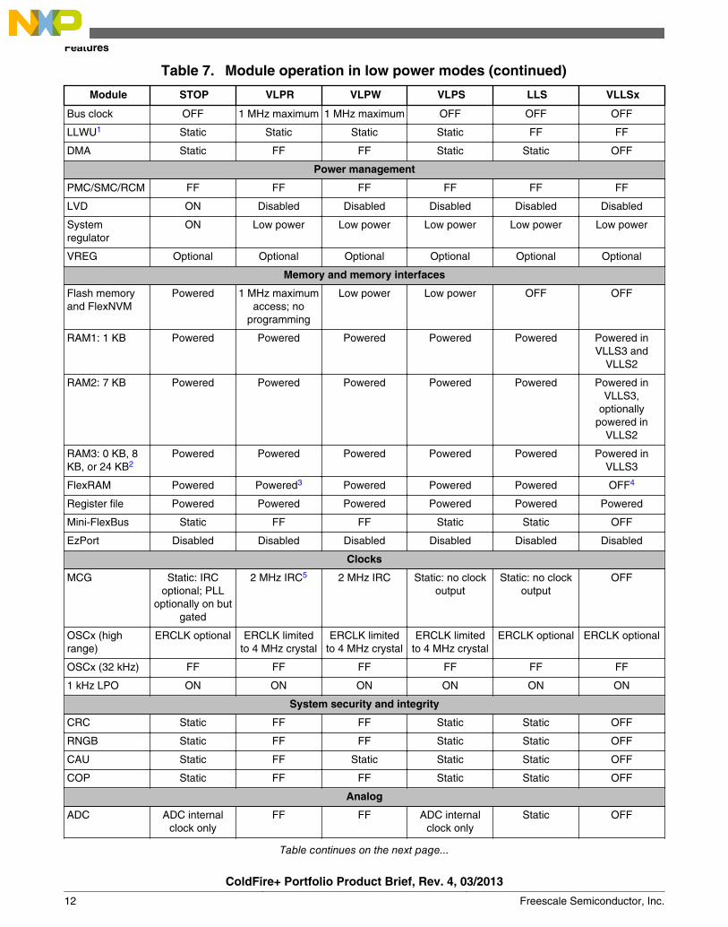
Table 7. Module operation in low power modes (continued)
Module STOP VLPR VLPW VLPS LLS VLLSx
Bus clock OFF 1 MHz maximum 1 MHz maximum OFF OFF OFF
LLWU1 Static Static Static Static FF FF
DMA Static FF FF Static Static OFF
Power management
PMC/SMC/RCM FF FF FF FF FF FF
LVD ON Disabled Disabled Disabled Disabled Disabled
Systemregulator
ON Low power Low power Low power Low power Low power
VREG Optional Optional Optional Optional Optional Optional
Memory and memory interfaces
Flash memoryand FlexNVM
Powered 1 MHz maximumaccess; no
programming
Low power Low power OFF OFF
RAM1: 1 KB Powered Powered Powered Powered Powered Powered inVLLS3 and
VLLS2
RAM2: 7 KB Powered Powered Powered Powered Powered Powered inVLLS3,
optionallypowered in
VLLS2
RAM3: 0 KB, 8KB, or 24 KB2
Powered Powered Powered Powered Powered Powered inVLLS3
FlexRAM Powered Powered3 Powered Powered Powered OFF4
Register file Powered Powered Powered Powered Powered Powered
Mini-FlexBus Static FF FF Static Static OFF
EzPort Disabled Disabled Disabled Disabled Disabled Disabled
Clocks
MCG Static: IRCoptional; PLL
optionally on butgated
2 MHz IRC5 2 MHz IRC Static: no clockoutput
Static: no clockoutput
OFF
OSCx (highrange)
ERCLK optional ERCLK limitedto 4 MHz crystal
ERCLK limitedto 4 MHz crystal
ERCLK limitedto 4 MHz crystal
ERCLK optional ERCLK optional
OSCx (32 kHz) FF FF FF FF FF FF
1 kHz LPO ON ON ON ON ON ON
System security and integrity
CRC Static FF FF Static Static OFF
RNGB Static FF FF Static Static OFF
CAU Static FF Static Static Static OFF
COP Static FF FF Static Static OFF
Analog
ADC ADC internalclock only
FF FF ADC internalclock only
Static OFF
Table continues on the next page...
Features
ColdFire+ Portfolio Product Brief, Rev. 4, 03/2013
12 Freescale Semiconductor, Inc.

Table 7. Module operation in low power modes (continued)
Module STOP VLPR VLPW VLPS LLS VLLSx
CMP HS or LScompare6
FF FF HS or LScompare6
LS compare7 LS compare7,8
6-bit DAC(integrated withCMP)
Static FF FF Static Static Static
VREF FF FF FF FF Static OFF
12-bit DAC Static FF FF Static Static Static
Timers
FTM Static FF FF Static Static OFF
MTIM Static FF FF Static Static OFF
PDB Static FF FF Static Static OFF
LPTMR FF FF FF FF FF FF
CMT Static FF FF Static Static OFF
Communication interfaces
UART Static, wakeupon edge
125 kbps 125 kbps Static, wakeupon edge
Static OFF
SPI Static 500 kbps inmaster mode,250 kbps inslave mode
500 kbps inmaster mode,250 kbps inslave mode
Static Static OFF
I2C Static, addressmatch wakeup
50 kbps 50 kbps Static, addressmatch wakeup
Static OFF
USB FS/LS Static Static Static Static Static OFF
USB DCD Static FF FF Static Static OFF
I2S/SAI FF with externalclock9
Maximum2 Mbps
Maximum2 Mbps
Maximum2 Mbps9
Static OFF
Human-machine interface (HMI)
EGPIO Wakeup FF FF Wakeup Static, pinslatched
OFF, pinslatched
RGPIO Static FF FF Static Static OFF
TSI Wakeup FF FF Wakeup Wakeup10 Wakeup10
IRQ Wakeup FF FF Wakeup Static, pinslatched
OFF, pinslatched
1. Using the LLWU module, the external pins available for this MCU do not require the associated peripheral function to beenabled. The only requirement is for the function controlling the pin (GPIO or peripheral) to be configured as an input toallow a transition to occur to the LLWU.
2. For the RAM3 size on a particular device, refer to the total RAM size provided in Feature Summary by Package.3. In VLPR mode, FlexRAM enabled as EEPROM is not writable (writes are ignored) but can be read. There are no access
restrictions in VLPR mode for FlexRAM configured as traditional RAM.4. FlexRAM is always powered off in VLLSx modes.5. Before executing an entry to VLPR mode, the MCG must be in one of two of its operating modes, each with a particular
clock source selected:• Either the MCG must be in its BLPE operating mode with only the low gain oscillator selected, or• The MCG must be in its BLPI operating mode with only the 2 MHz IRC selected.
6. The CMP in stop or VLPS mode supports high speed or low speed, external pin-to-pin or external pin-to-DAC compares.Windowed, sampled, and filtered modes of operation are not available in stop, VLPS, LLS, or VLLSx modes.
Features
ColdFire+ Portfolio Product Brief, Rev. 4, 03/2013
Freescale Semiconductor, Inc. 13

7. The CMP in LLS or VLLSx mode supports only low speed, external pin-to-pin or external pin-to-DAC compares.Windowed, sampled, and filtered modes of operation are not available in stop, VLPS, LLS, or VLLSx modes.
8. In VLLSx modes, the CMP0_OUT signal is gated until after MCU recovery.9. Use an externally generated bit clock or an externally generated audio master clock (including EXTAL).10. TSI wakeup from LLS and VLLSx modes is limited to a single selectable pin.
NOTE• ON means the module is operational by default in the designated power mode.• FF means "full functionality." The user has the option to enable the module's
operation in the designated power mode. In VLPR and VLPW modes, the systemfrequency might limit some modules.
• Static means the digital modules' register states and associated memories are held.• Powered means memory is powered to retain contents.• Low power means flash has a low power state that retains configuration registers to
support faster wakeup.• Wakeup means the module can serve as a wakeup source for the chip.• OFF means the module is powered off and is in a reset state upon wakeup.
4.4 Module-by-Module Feature ListThese descriptions extend the feature summaries.
Core and System
4.4.1.1 32-bit Version 1 ColdFire Central Processing Unit (CPU)
• Up to 50 MHz V1 Coldfire CPU from 1.71 V to 3.6 V across temperature range of –40ºC to 105ºC• Two-stage instruction fetch pipeline (IFP) (plus optional instruction buffer stage)• Two-stage operand execution pipeline (OEP)• Dhrystone 2.1 performance:
• 1.10 DMIPS per MHz performance when running from internal RAM• 0.99 DMIPS per MHz when running from flash
• Implements instruction set architecture C (ISA_C)• EMAC and hardware DIV modules
4.4.1.2 Debug
• Integrated ColdFire DEBUG_Rev_B+ interface with single wire BDM connection• Real-time debug support, with six hardware breakpoints (four PC, one address pair, and one data) that can be
configured into 1- or 2-level triggers and can be configured to halt the processor or generate debug interrupt• Capture of compressed processor status and debug data into on-chip trace buffer provides program (and optional slave
bus data) trace capabilities• On-chip trace buffer provides programmable start/stop recording conditions• Debug resources are accessible via single-pin BDM interface or the privileged WDEBUG instruction
4.4.1.3 V1 ColdFire Interrupt Controller (CF1_INTC)
• Support for up to 44 peripheral I/O interrupt requests and 7 software interrupt requests (1 per level)
4.4.1
Core and System
ColdFire+ Portfolio Product Brief, Rev. 4, 03/2013
14 Freescale Semiconductor, Inc.
• Fixed association between interrupt request source and level plus priority; up to two requests can be remapped to thehighest maskable level plus priority
• Unique vector number for each interrupt source• Support for service routine interrupt acknowledge (software IACK) read cycles for improved system performance
4.4.1.4 Crossbar Switch
• Hardware interconnect matrix interfacing bus masters to bus slaves• Two-stage pipelined system bus protocol• Support for concurrent data transfers to all crossbar slave targets• Programmable fixed priority or round robin arbitration
4.4.1.5 DMA Controller
• Four independently programmable DMA controller channels provides the means to directly transfer data betweensystem memory and I/O peripherals
• DMA controller is capable of functioning in run and wait modes of operation• Dual-address transfers via 32-bit master connection to the system bus• Data transfers in 8-, 16-, or 32-bit blocks• Continuous-mode or cycle-steal transfers from software or peripheral initiation• One programmable input selected from 16 possible peripheral requests per channel
Power Management
4.4.2.1 Power Management Controller (PMC)
• Separate digital (regulated) and analog (referenced to digital) supply outputs• Programmable low power modes• No output supply decoupling capacitors required• Wake-up from low power modes via internal modules and external inputs• Integrated Power-on Reset (POR) providing brownout detection in all power modes• Integrated Low Voltage Detect (LVD) with reset capability• Selectable LVD trip points• Programmable Low Voltage Warning (LVW) interrupt capability• Buffered bandgap reference voltage output• Factory programmed trim for bandgap and LVD• 1 kHz Low Power Oscillator (LPO)
4.4.2.2 Voltage Regulator (VREG)
• 3.3 V regulated output can power MCU main power supply• Output pin from regulator can power external board components and source up to 120 mA maximum• Eliminates cost of external LDO• For devices with integrated USB controller:
• 5 V regulator input typically provided by USB VBUS power• 3.3 V regulated output powers on-chip USB transceiver
4.4.2
Power Management
ColdFire+ Portfolio Product Brief, Rev. 4, 03/2013
Freescale Semiconductor, Inc. 15

Memory and Memory Interfaces
4.4.3.1 On-Chip Memory
• Up to 160 KB flash memory read/program/erase over full operating voltage and temperature• Up to 128 KB program flash array• FlexMemory for additional data/program space or up to 2 KB enhanced EEPROM
• 32 KB FlexNVM• 2 KB FlexRAM (can be used as normal RAM if enhanced EEPROM is not used)
• Separate block protection for standard flash array and FlexMemory (including data and EEPROM)• Up to 32 KB random access memory (RAM)• 32-byte register file, powered in all modes• Security circuitry to prevent unauthorized access to RAM and flash contents
4.4.3.2 External Bus Interface (Mini-FlexBus)
• Two independent, user-programmable chip-select signals that can gluelessly interface with external RAM, PROM,EPROM, EEPROM, flash, and other peripherals
• 8-bit and 16-bit port sizes with configuration for multiplexed or nonmultiplexed address and data buses• Byte, word, and longword transfers• Programmable address-setup time with respect to the assertion of chip select• Programmable address-hold time with respect to the negation of chip select and transfer direction
4.4.4 Clocks• Frequency-locked loop (FLL)
• Digitally controlled oscillator (DCO) with programmable frequency range• Option to program DCO frequency for a 32.768 kHz external reference clock source• Internal or external reference clock can be used to control the FLL
• Phase-locked loop (PLL)• Voltage-controlled oscillator (VCO)• External reference clock is used as the PLL source• Modulo VCO frequency divider phase/frequency detector• Integrated loop filter
• Internal reference clock (IRC) generator• 32 kHz low range clock with 9 trim bits for accuracy• 2 MHz fast clock with 3 trim bits• Low range clock can be used to control the FLL• Low range or fast clock can be selected as MCU's clock source• Can be used as a clock source for other on-chip peripherals
• External clock (ERCLK) from the Crystal Oscillator (XOSC)• Can be used as the FLL and/or PLL source• Can be selected as the clock source for the MCU
• External clock monitor with reset request capability• Lock detector with interrupt request capability for use with the PLL• Auto Trim Machine (ATM) for trimming both the low range and fast internal reference clocks• Reference dividers for both the FLL and PLL are provided• Clock source selected can be divided down by 1, 2, 4, 8, or 16
4.4.3
Memory and Memory Interfaces
ColdFire+ Portfolio Product Brief, Rev. 4, 03/2013
16 Freescale Semiconductor, Inc.

System Security and Integrity
4.4.5.1 Cryptographic Acceleration Unit (CAU)
• Tightly coupled execution unit accessed with ColdFire coprocessor instructions• Hardware acceleration of the following cryptographic algorithms: DES, AES-128, AES-192, AES-256, MD5, SHA-1,
and SHA-256 (enables more complex algorithms such as 3DES with software encryption libraries that use these basichardware security blocks)
• Simple, flexible programming model; very efficient ASM library is provided• ColdFire CAU Software Library: available at http://freescale.com
4.4.5.2 Random Number Generator (RNGB)
• National Institute of Standards and Technology (NIST)-capable pseudo-random number generator (reference: http://csrc.nist.gov )
• Support for the key generation algorithm defined in the Digital Signature Standard (reference: http://www.itl.nist.gov/fipspubs/fip186.htm )
• Integrated entropy sources capable of providing the RNGB with entropy for its seed
4.4.5.3 Cyclic Redundancy Check (CRC)
• Hardware CRC generator circuit using 16-bit or 32-bit (programmable) shift register• Programmable initial seed value and polynomial• Error detection for all single, double, and odd errors as well as most multibit errors• Optional feature to transpose input data and CRC result via transpose register (required for certain CRC standards)• Final XOR of the output (some CRCs have final XOR of their checksum with protocol-specified value)
4.4.5.4 COP Watchdog Module
• Independent clock source input (independent from CPU/bus clock)• Choice between two clock sources:
• LPO oscillator• Bus clock
Analog
4.4.6.1 16-bit Successive Approximation Analog-to-Digital Converter(ADC)
• Linear successive approximation algorithm with up to 16-bit resolution• Output modes:
• Differential 16-bit, 13-bit, 11-bit, and 9-bit modes, in two's complement 16-bit sign-extended format• Single-ended 16-bit, 12-bit, 10-bit, and 8-bit modes, in right-justified unsigned format
• Single or continuous conversion• Configurable sample time and conversion speed/power• Conversion complete and hardware average complete flag and interrupt
4.4.5
4.4.6
System Security and Integrity
ColdFire+ Portfolio Product Brief, Rev. 4, 03/2013
Freescale Semiconductor, Inc. 17

• Input clock selectable from up to four sources• Operation in low power modes for lower noise operation• Asynchronous clock source for lower noise operation with option to output the clock• Selectable asynchronous hardware conversion trigger with hardware channel select• Automatic compare with interrupt for various programmable values• Temperature sensor• Hardware average function• Selectable voltage reference• Self-calibration mode
4.4.6.2 12-bit Successive Approximation Analog-to-Digital Converter(ADC)
• Linear successive approximation algorithm with up to 12-bit resolution• Single-ended 12-bit, 10-bit, and 8-bit modes, in right-justified unsigned format• Single or continuous conversion• Configurable sample time and conversion speed/power• Conversion complete and hardware average complete flag and interrupt• Input clock selectable from up to four sources• Operation in low power modes for lower noise operation• Asynchronous clock source for lower noise operation with option to output the clock• Selectable asynchronous hardware conversion trigger with hardware channel select• Automatic compare with interrupt for various programmable values• Temperature sensor• Hardware average function• Selectable voltage reference• Self-calibration mode
4.4.6.3 High-Speed Comparator (CMP)
• Up to eight selectable comparator inputs; each input can be compared with any input by any polarity sequence• Selectable inversion on comparator output• Comparator output supports:
• Sampled• Windowed (ideal for certain PWM zero-crossing-detection applications)• Digitally filtered using external sample signal or scaled peripheral clock
• Selectable interrupt on rising edge, falling edge, or either rising or falling edges of comparator output• Two performance modes:
• Shorter propagation delay at the expense of higher power• Low power, with longer propagation delay
• Operational in all MCU power modes
4.4.6.3.1 6-bit Digital-to-Analog Converter (DAC)
• Integrated on high-speed comparator• 6-bit resolution• On-chip programmable reference generator output• Selectable supply reference source• Operational in all MCU power modes
Analog
ColdFire+ Portfolio Product Brief, Rev. 4, 03/2013
18 Freescale Semiconductor, Inc.

4.4.6.4 12-bit Digital-to-Analog Converter (DAC)
• 12-bit resolution• Guaranteed 6-sigma monotonicity over input word• High-speed and low-speed conversions: 1 µs conversion rate for high speed, 2 µs for low speed• Power-down mode• Choice of asynchronous or synchronous updates• Automatic mode allows the DAC to generate its own output waveforms including square, triangle, and sawtooth• Automatic mode allows programmable period, update rate, and range• DMA support with configurable watermark level
4.4.6.5 Voltage Reference (VREF)
• Programmable trim register with 0.5 mV steps, automatically loaded with room temperature value upon reset• Programmable mode selection:
• Off• Bandgap out (or stabilization delay)• Low-power buffer mode• Tight-regulation buffer mode
• 1.2 V output at room temperature• Dedicated output pin
Timers
4.4.7.1 FlexTimer (FTM)
• Selectable FTM source clock• Programmable prescaler• 16-bit counter supporting free-running or initial/final value, and counting is up or up-down• Input capture, output compare, and edge-aligned and center-aligned PWM modes• Input capture and output compare modes• Operation of FTM channels as pairs with equal outputs, pairs with complementary outputs, or independent channels
with independent outputs• Deadtime insertion is available for each complementary pair• Generation of hardware triggers• Software control of PWM outputs• Configurable channel polarity• Programmable interrupt on input capture, reference compare, overflowed counter, or detected fault condition
4.4.7.2 Carrier Modulator Transmitter (CMT)
• Four modes of operation• Time with independent control of high and low times• Baseband• Frequency shift key (FSK)• Direct software control of IRO pin
• Extended space operation in time, baseband, and FSK modes• Selectable input clock divide• Interrupt on end of cycle
4.4.7
Timers
ColdFire+ Portfolio Product Brief, Rev. 4, 03/2013
Freescale Semiconductor, Inc. 19
• Ability to disable IRO pin and use as timer interrupt• DMA Support
4.4.7.3 Programmable Delay Block (PDB)
• 16-bit resolution with prescaler• Positive transition of trigger event signal initiates the counter• Supports two triggered delay outputs signals, each with an independently controlled delay from the trigger event• Outputs can be ORed together to schedule two conversions from one input trigger event• Outputs can schedule precise edge placement for a pulsed output. This feature is used to generate the control signal for
the CMP's windowing feature and output to a package pin if needed for applications, such as critical conductive modepower factor correction.
• Continuous-pulse output or single-shot mode supported• Supports bypass mode• Each output is independently enabled• Seven possible trigger events
4.4.7.4 Modulo Timer (MTIM)
• 16-bit up-counter• Free-running or 16-bit modulo• Software controllable interrupt on overflow• Counter reset bit (TRST)• Counter stop bit (TSTP)
• Four software selectable clock sources for input to prescaler:• System bus clock — rising edge• Fixed frequency clock (XCLK) — rising edge• External clock source on the TCLK pin — rising edge• External clock source on the TCLK pin — falling edge
• Nine selectable clock prescale values:• Clock source divide by 1, 2, 4, 8, 16, 32, 64, 128, or 256
4.4.7.5 Low Power Timer (LPT)
• Operation as timer or pulse counter• Selectable clock for prescaler/glitch filter
• 1 kHz internal LPO• External low power crystal oscillator• Internal reference clock (not available in low leakage power modes)• Secondary external reference clock (for example, 32 kHz crystal)
• Configurable glitch filter or prescaler with 5-bit counter• Interrupt generated on timer compare• Hardware trigger generated on timer compare
Communication Interfaces
4.4.8.1 USB On-the-Go Controller
• USB 1.1 and 2.0 compliant full-speed device/Host controller
4.4.8
Communication Interfaces
ColdFire+ Portfolio Product Brief, Rev. 4, 03/2013
20 Freescale Semiconductor, Inc.

• On-the-Go protocol logic• 16 bidirectional endpoints• DMA or FIFO data stream interfaces• Low-power consumption
4.4.8.2 USB Device Charge Detect (DCD)
• Compliant with the latest industry standard specification, USB Battery Charging Specification, Revision 1.1• Compatible with systems powered from:
• Rechargeable battery• Nonrechargeable battery• External 3.3 V LDO regulator powered from USB or directly from USB using internal regulator
• Programmable event timers for flexibility and better compatibility with future udpates to the standards• Minimal configuration required:
• Set the clock frequency and enable the module• Preprogrammed default values ensure compatibility with the USB Battery Charging Specification, Revision 1.1
4.4.8.3 Inter-IC Sound (I2S) / Synchronous Audio Interface (SAI)
• Support for full-duplex serial interfaces with frame synchronization such as I2S, AC97, and CODEC/DSP interfaces• Two independent bit clock / frame sync pairs• Four software configurable transmit or receive channels that can be software allocated to any bit clock / frame sync pair• Independent 16 word x 32-bit FIFO per channel• Graceful restart after FIFO Error• Operation in stop modes
4.4.8.4 Universal Asynchronous Receiver/Transmitter (UART)
• Support for ISO 7816 protocol for interfacing with smart cards• Full-duplex operation• Standard mark/space non-return-to-zero (NRZ) format• 13-bit baud rate selection with fractional divide of 32• Programmable 8-bit or 9-bit data format• Separately enabled transmitter and receiver• Programmable transmitter output polarity• Programmable receive input polarity• 13-bit break character option• 11-bit break character detection option• Parameterizable buffer support for one dataword for each transmit and receive• Independent FIFO structure for transmit and receive• Two receiver wakeup methods:
• Idle line wakeup• Address mark wakeup
• Address match feature in receiver to reduce address mark wakeup ISR overhead• Ability to select MSB or LSB to be first bit on wire• Hardware flow control support for request to send (RTS) and clear to send (CTS) signals• Interrupt-driven operation with 11 flags:
• Transmitter data buffer at or below watermark• Transmission complete• Receiver data buffer at or above watermark• Idle receiver input• Receiver overrun
Communication Interfaces
ColdFire+ Portfolio Product Brief, Rev. 4, 03/2013
Freescale Semiconductor, Inc. 21

• Receiver data buffer underflow• Noise error• Framing error• Parity error• Active edge on receive pin• LIN break detect
• Receiver framing error detection• Hardware parity generation and checking• 1/16 bit-time noise detection• 5 channel DMA requests
4.4.8.5 Inter-Integrated Circuit (I2C)
• Compatible with I2C bus standard and SMBus Specification Version 2 features• Up to 100 kbps with maximum bus loading• Multimaster operation• Software programmable for one of 64 different serial clock frequencies• Programmable slave address and glitch input filter• Interrupt driven byte-by-byte data transfer or DMA support• Arbitration lost interrupt with automatic mode switching from master to slave• Calling address identification interrupt• Bus busy detection broadcast and 10-bit address extension• Address matching causes wakeup when processor is in low power modes
4.4.8.6 Serial Peripheral Interface (SPI)
• Master and slave mode• Full-duplex, three-wire synchronous transfers• Programmable transmit bit rate• Double-buffered transmit and receive data registers• Serial clock phase and polarity options• Slave select output• Mode fault error flag with CPU interrupt capability• Control of SPI operation during wait mode• Selectable MSB-first or LSB-first shifting• Programmable 8-bit or 16-bit data transmission length• Receive data buffer hardware match feature• 64-bit FIFO mode for high speed transfers of large amounts of data (SPI0 only)• Support for both transmit and receive by DMA
Human-Machine Interface (HMI)
4.4.9.1 Touch Sensing Input (TSI)
• Support for as many as 16 input capacitive touch sensing pins with individual result registers• Automatic detection of Electrode Capacitance Change with programmable upper and lower threshold• Automatic periodic scan unit with different duty cycles for run and low power modes• Full support (with Freescale's touch sensing software library suite) for implementing keypads, rotaries, and sliders• Operation across all low power modes: wait, stop, VLPR, VLPW, VLPS, LLS, VLLSx• Capability to wake MCU from low power modes
4.4.9
Human-Machine Interface (HMI)
ColdFire+ Portfolio Product Brief, Rev. 4, 03/2013
22 Freescale Semiconductor, Inc.

• Configurable interrupts:• End-of-Scan or Out-of-Range interrupt• TSI Error Interrupts: pad short to Vdd/Vss or Conversion Overrun
• Standalone operation not requiring any external crystal even in low power modes• Configurable integration of each electrode capacitance measurement from 1 to 32 times• Programmable Electrode Oscillator and TSI Reference Oscillator for high sensitivity, small scan time, and low power
functionality• Only one pin per electrode implementation with no external hardware required
4.4.9.2 Enhanced General Purpose Input/Output (EGPIO)
• Programmable glitch filter on up to 16 input pins and interrupt with selectable polarity on all input pins• Hysteresis and configurable pullup/pulldown device on all input pins• Configurable slew rate and drive strength on all output pins• Independent pin value register to read logic level on digital pin
4.4.9.3 Rapid General Purpose Input/Output (RGPIO)
• Package pin toggle rates typically faster than comparable pins mapped onto peripheral bus• 16 bits of high-speed GPIO functionality in memory-mapped device connected to the ColdFire core's local 32-bit bus
• All reads and writes complete in a single data phase cycle for zero wait-state response• Data bits can be accessed directly or via alternate addresses to provide set, clear, and toggle functions• Unique data direction and pin enable control registers
5 Developer EnvironmentFreescale's ColdFire products are supported by a widespread, established network of tools and third party developers andsoftware vendors. The ColdFire+ MCU families take advantage of these and similar development resources.
5.1 Freescale's Tower System SupportFreescale's Tower System is a modular development platform for 8-bit, 16-bit, and 32-bit microcontrollers that enablesadvanced development through rapid prototyping. Featuring multiple development boards or modules, the Tower Systemprovides designers with building blocks for entry-level to advanced microcontroller development.
Developer Environment
ColdFire+ Portfolio Product Brief, Rev. 4, 03/2013
Freescale Semiconductor, Inc. 23

The Freescale Tower System
MCU/MPU Module
• Tower controller board
• Works stand-alone or in Tower System
• Features new on-board debug interface for easy programming and debugging via mini-B USB cable
Secondary Elevator
• Additional serial and expansion buses and peripheral interfaces
Peripheral Module
• (i.e. serial, prototype, etc.)
Size
• Tower is approx. 3.5” H x 3.5” W x 3.5” D when fully assembled
Primary Elevator
• Common serial and expansion bus signals
• Two 2x80 connectors on backside for easy signal access and side-mounting board (i.e. LCD module)
• Power regulation circuitry
• Standardized signal assignments
Board Connectors
• Four card-edge connectors
• Uses PCI Express® connectors (x16, 90 mm/3.5” long, 164 pins)
Figure 3. Freescale's Tower System
Table 8. Tower Modules for ColdFire+ MCU Families
Microcontroller Modules Features
ColdFire+ JF Family MCU Module
TWR-MCF51JF
TWR-MCF51JF-KIT (contains TWR-ELEV andTWR-PROTO)
JF family 128 KB flash MCU in 64 LQFP package
On-board BDM debug interface
Access to all features
ColdFire+ QM Family MCU Module
TWR-MCF51QM
TWR-MCF51QM-KIT (contains TWR-ELEV andTWR-PROTO)
QM family 128 KB flash MCU in 64 LQFP package
On-board BDM debug interface
Access to all features
Developer Environment
ColdFire+ Portfolio Product Brief, Rev. 4, 03/2013
24 Freescale Semiconductor, Inc.
5.2 CodeWarrior Development StudioFreescale's CodeWarrior Development Studio for Microcontrollers v10.x integrates the development tools for the RS08,HCS08, ARM, ColdFire, and ColdFire+ architectures into a single product based on the Eclipse open development platform.Eclipse offers an excellent framework for building software development environments and is becoming a standardframework used by many embedded software vendors.
• Eclipse IDE 3.4• Build system with optimizing C/C++ compilers for RS08, HCS08, ARM, ColdFire, and ColdFire+ processors• Extensions to Eclipse C/C++ Development Tools (CDT) to provide sophisticated features to troubleshoot and repair
embedded applications
Table 9. CodeWarrior 10.x Differentiating Features
Differentiatingfeatures
Customerbenefits
Details
MCU ChangeWizard
Ability toeasilyretargetproject to anewprocessor
Simply select a new device (from the same or a different architecture) and select thedefault connection, and the CodeWarrior tool suite automatically reconfigures the projectfor the new device with the correct build tools and support files.
• Compiler• Assembler• Linker• Header files• Vector tables• Libraries• Linker configuration files
FreescaleProcessor Expert
Problems inhardwarelayer can beresolvedduring initialdesign phase
Combines easy-to-use component-based application creation with an expert knowledgesystem.
• CPU, on-chip peripherals, external peripherals, and software functionality areencapsulated into embedded components
• Each component’s functionality can be tailored to fit application requirements bymodifying the component’s properties, methods and events
• When the project is built, Processor Expert automatically generates highly optimizedembedded C code and places the source files into the project
• Graphical user interface: Allows an application to be specified by the functionalityneeded
• Automatic code generator: Creates tested, optimized C code tuned to applicationneeds and the selected Freescale device
• Built-in knowledgebase: Immediately flags resource conflicts and incorrect settings,so errors are caught early in design cycle
• Component wizard: Allows user-specific, hardware-independent embeddedcomponents to be created
Trace and profilesupport for on-chip trace buffers
Sophisticatedemulator-likedebugcapabilitywithoutadditionalhardware
The CodeWarrior profiling and analysis tools provide visibility into an application as it runson the processor to identify operational problems.
• Supports architectures with on-chip trace buffers (HCS08, V1 ColdFire, ARM)• Allows tracepoints to be set to enable and disable trace output• Can step through trace data and the corresponding source code simultaneously• Allows trace data to be exported into a Microsoft® Excel® file
Developer Environment
ColdFire+ Portfolio Product Brief, Rev. 4, 03/2013
Freescale Semiconductor, Inc. 25

5.3 Freescale's MQX™ Software SolutionsThe increasing complexity of industrial applications and expanding functionality of semiconductors are driving embeddeddevelopers toward solutions that combine proven hardware and software platforms. These solutions help accelerate time tomarket and improve application development success.
Freescale Semiconductor offers the MQX real-time operating system (RTOS), with TCP/IP and USB software stacks andperipheral drivers, to customers of ColdFire and ColdFire+ MCUs at no additional charge. The combination of Freescale'sMQX software solutions and Freescale's silicon portfolio creates a comprehensive source for hardware, software, tools, andservices.
Application
HAL
Hardware
On Device PC Hosted
CodeWarrior™ Development Environment
(MQX OS Aware)
CodeWarrior Processor Expert™
MQX Design and
Development Tools
Third Party: IAR
(MQX OS Aware)
Open Source BDM and
Third Party: Emulator/Probe
Demo Code ApplicationsCustomized ApplicationsApplication Tasks and
Industry-Specific Libraries
BSP/PSP
Microcontroller
Freescale Comprehensive Solution
Enablement Layer
Ethernet (RTCS)
File System
USB
CAN
MQX RTOS Optional Services
Core Services MQX RTOS
Discrete Driver, Third Party and
Freescale
BDM/JTAG
Figure 4. MQX Comprehensive Solution
Key benefits of Freescale's MQX RTOS include:
• Small memory footprint: The RTOS was designed for speed and size efficiency in embedded systems. It delivers truereal-time performance, with context switching and low-level interrupt routines hand-optimized in assembly.
• Component-based architecture: Provides a fully-functional RTOS core with additional, optional services. Freescale'sMQX RTOS includes 25 components (8 core components and 17 optional). Components are linked in only if needed,preventing unused functions from bloating the memory footprint.
Developer Environment
ColdFire+ Portfolio Product Brief, Rev. 4, 03/2013
26 Freescale Semiconductor, Inc.

• Full and lightweight components: Key components are included in both full and lightweight versions for further controlof size, RAM/ROM utilization, and performance options.
• Real-time, priority-based, preemptive multithreading: Allows high-priority threads to meet their deadlines consistently,no matter how many other threads are competing for CPU time.
• Scheduling: Enables faster development time by offloading from developers the task of creating or maintaining anefficient scheduling system and interrupt handling.
• Code reuse: Provides a framework with a simple, intuitive API to build and organize the features across Freescale’sbroad portfolio of embedded processors.
• Fast boot sequence: Ensures the application is running quickly after the hardware has been reset.• Simple Message Passing: Messages can be passed either from a system pool or a private pool, sent with either urgent
status or a user-defined priority, and broadcast or task specific. For maximum flexibility, a receiving task can operateon either the same CPU as the sending task or on a different CPU within the same system.
MQX RTOS—Customizable Component Set
Task Errors Utilities
Initialization Core Memory
Services Automatic Task
Creation
Lightweight Semaphores
Task Queue Scheduling
RR and FIFO Scheduling
Queues Name
Services Interrupts
Messages
Events
Mutexes
IPCs Exception Handling
Kernel Log Logs
I/O Subsystems
Formatted I/O
Timers
Watchdogs
Task Management
Partitions
As-Needed
Core
Semaphores
Figure 5. MQX Customizable Component Set
5.4 Additional Software Stacks Provided• Complimentary software driver library for the hardware Cryptographic Acceleration Unit (CAU) provides basic
encryption for all functions directly supported by the hardware: DES, AES-128, AES-192, AES-256, SHA-1,SHA-256, and MD5
• Complimentary ColdFire/ColdFire+ Digital Signal Processing Library using the EMAC hardware unit• Complimentary Bare-metal/No OS USB Stack complete with Personal Health Card Device (PHDC), Mass Storage
(MSC), Communications Device (CDC), human interface device (HID), and audio classes• Touch Sensing Software Suite
Developer Environment
ColdFire+ Portfolio Product Brief, Rev. 4, 03/2013
Freescale Semiconductor, Inc. 27

• Complimentary Freescale embedded graphical user interface (eGUI): http://www.freescale.com/egui• Bootloaders (USB, RF, serial)
6 Revision HistoryThe following table summarizes updates since the release of the prior version.
Table 10. Revision History
Revision Date Substantial Changes
3 08/2012 Removed references to discontinued QF and QH families.
4 03/2013 Updated 32-bit Version 1 ColdFire Central Processing Unit (CPU) feature list.
Revision History
ColdFire+ Portfolio Product Brief, Rev. 4, 03/2013
28 Freescale Semiconductor, Inc.

How to Reach Us:
Home Page:www.freescale.com
Web Support:http://www.freescale.com/support
USA/Europe or Locations Not Listed:Freescale SemiconductorTechnical Information Center, EL5162100 East Elliot RoadTempe, Arizona 85284+1-800-521-6274 or +1-480-768-2130www.freescale.com/support
Europe, Middle East, and Africa:Freescale Halbleiter Deutschland GmbHTechnical Information CenterSchatzbogen 781829 Muenchen, Germany+44 1296 380 456 (English)+46 8 52200080 (English)+49 89 92103 559 (German)+33 1 69 35 48 48 (French)www.freescale.com/support
Japan:Freescale Semiconductor Japan Ltd.HeadquartersARCO Tower 15F1-8-1, Shimo-Meguro, Meguro-ku,Tokyo 153-0064Japan0120 191014 or +81 3 5437 [email protected]
Asia/Pacific:Freescale Semiconductor China Ltd.Exchange Building 23FNo. 118 Jianguo RoadChaoyang DistrictBeijing 100022China+86 10 5879 [email protected]
Document Number: MCF51JxQxPBRev. 4, 03/2013
Information in this document is provided solely to enable system and softwareimplementers to use Freescale Semiconductors products. There are no express or impliedcopyright licenses granted hereunder to design or fabricate any integrated circuits orintegrated circuits based on the information in this document.
Freescale Semiconductor reserves the right to make changes without further notice to anyproducts herein. Freescale Semiconductor makes no warranty, representation, orguarantee regarding the suitability of its products for any particular purpose, nor doesFreescale Semiconductor assume any liability arising out of the application or use of anyproduct or circuit, and specifically disclaims any liability, including without limitationconsequential or incidental damages. "Typical" parameters that may be provided inFreescale Semiconductor data sheets and/or specifications can and do vary in differentapplications and actual performance may vary over time. All operating parameters,including "Typicals", must be validated for each customer application by customer'stechnical experts. Freescale Semiconductor does not convey any license under its patentrights nor the rights of others. Freescale Semiconductor products are not designed,intended, or authorized for use as components in systems intended for surgical implantinto the body, or other applications intended to support or sustain life, or for any otherapplication in which failure of the Freescale Semiconductor product could create asituation where personal injury or death may occur. Should Buyer purchase or useFreescale Semiconductor products for any such unintended or unauthorized application,Buyer shall indemnify Freescale Semiconductor and its officers, employees, subsidiaries,affiliates, and distributors harmless against all claims, costs, damages, and expenses, andreasonable attorney fees arising out of, directly or indirectly, any claim of personal injuryor death associated with such unintended or unauthorized use, even if such claims allegesthat Freescale Semiconductor was negligent regarding the design or manufacture ofthe part.
RoHS-compliant and/or Pb-free versions of Freescale products have the functionality andelectrical characteristics as their non-RoHS-complaint and/or non-Pb-free counterparts.For further information, see http://www.freescale.com or contact your Freescalesales representative.
For information on Freescale's Environmental Products program, go tohttp://www.freescale.com/epp.
Freescale™ and the Freescale logo are trademarks of Freescale Semiconductor, Inc.All other product or service names are the property of their respective owners.
© 2010–2013 Freescale Semiconductor, Inc.