CMOS VLSI Design DC Transfer Characteristics and Switch –level RC delay Models.
44
CMOS VLSI Design DC Transfer Characteristics and Switch –level RC delay Models
-
Upload
zachery-blakeway -
Category
Documents
-
view
238 -
download
3
Transcript of CMOS VLSI Design DC Transfer Characteristics and Switch –level RC delay Models.
CMOS VLSIDesign
DC Transfer Characteristics and Switch –level RC delay Models

Slide 2CMOS VLSI Design
DC Response DC Response: Vout vs. Vin for a gate
Ex: Inverter
– When Vin = 0 -> Vout = VDD
– When Vin = VDD -> Vout = 0
– In between, Vout depends on
transistor size and current– By KCL, must settle such that
Idsn = |Idsp|
– We could solve equations– But graphical solution gives more insight
Idsn
Idsp Vout
VDD
Vin
Slide 3CMOS VLSI Design
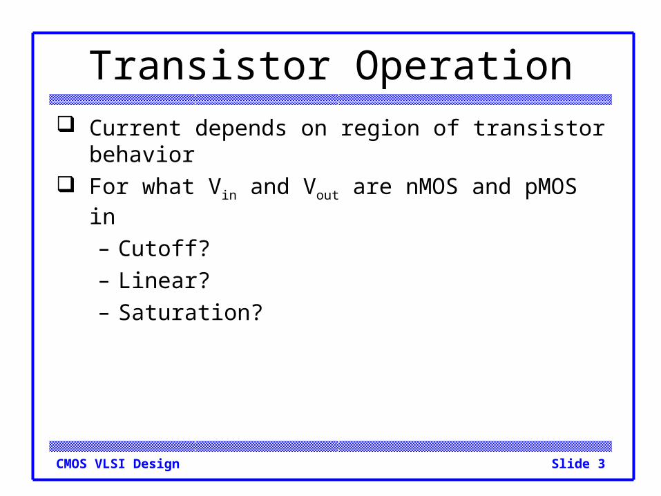
Transistor Operation Current depends on region of transistor behavior For what Vin and Vout are nMOS and pMOS in
– Cutoff?– Linear?– Saturation?

Slide 4CMOS VLSI Design
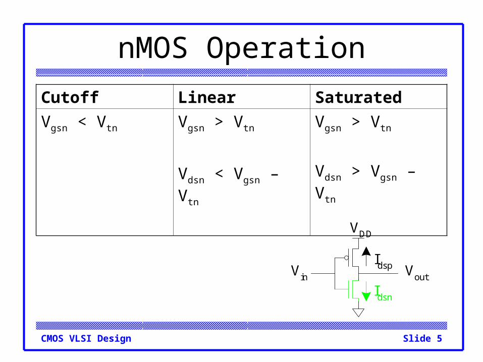
nMOS Operation
Cutoff Linear Saturated
Vgsn < Vgsn >
Vdsn <
Vgsn >
Vdsn >
Idsn
Idsp Vout
VDD
Vin
Slide 5CMOS VLSI Design
nMOS Operation
Cutoff Linear Saturated
Vgsn < Vtn Vgsn > Vtn
Vdsn < Vgsn – Vtn
Vgsn > Vtn
Vdsn > Vgsn – Vtn
Idsn
Idsp Vout
VDD
Vin

Slide 6CMOS VLSI Design
nMOS Operation
Cutoff Linear Saturated
Vgsn < Vtn Vgsn > Vtn
Vdsn < Vgsn – Vtn
Vgsn > Vtn
Vdsn > Vgsn – Vtn
Idsn
Idsp Vout
VDD
Vin
Vgsn = Vin
Vdsn = Vout

Slide 7CMOS VLSI Design
nMOS Operation
Cutoff Linear Saturated
Vgsn < Vtn
Vin < Vtn
Vgsn > Vtn
Vin > Vtn
Vdsn < Vgsn – Vtn
Vout < Vin - Vtn
Vgsn > Vtn
Vin > Vtn
Vdsn > Vgsn – Vtn
Vout > Vin - Vtn
Idsn
Idsp Vout
VDD
Vin
Vgsn = Vin
Vdsn = Vout
Slide 8CMOS VLSI Design
pMOS Operation
Cutoff Linear Saturated
Vgsp > Vgsp <
Vdsp >
Vgsp <
Vdsp <
Idsn
Idsp Vout
VDD
Vin

Slide 9CMOS VLSI Design
pMOS Operation
Cutoff Linear Saturated
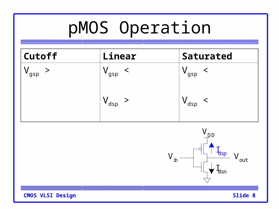
Vgsp > Vtp Vgsp < Vtp
Vdsp > Vgsp – Vtp
Vgsp < Vtp
Vdsp < Vgsp – Vtp
Idsn
Idsp Vout
VDD
Vin
Slide 10CMOS VLSI Design
pMOS Operation
Cutoff Linear Saturated
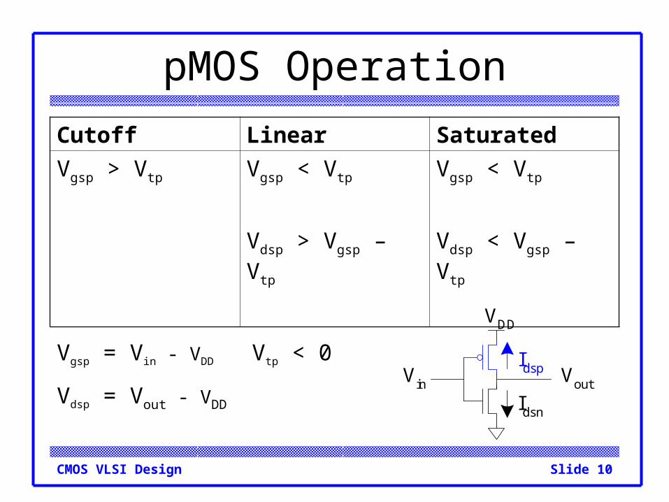
Vgsp > Vtp Vgsp < Vtp
Vdsp > Vgsp – Vtp
Vgsp < Vtp
Vdsp < Vgsp – Vtp
Idsn
Idsp Vout
VDD
Vin
Vgsp = Vin - VDD
Vdsp = Vout - VDD
Vtp < 0
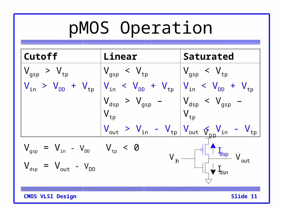
Slide 11CMOS VLSI Design
pMOS Operation
Cutoff Linear Saturated
Vgsp > Vtp
Vin > VDD + Vtp
Vgsp < Vtp
Vin < VDD + Vtp
Vdsp > Vgsp – Vtp
Vout > Vin - Vtp
Vgsp < Vtp
Vin < VDD + Vtp
Vdsp < Vgsp – Vtp
Vout < Vin - Vtp
Idsn
Idsp Vout
VDD
Vin
Vgsp = Vin - VDD
Vdsp = Vout - VDD
Vtp < 0

Slide 12CMOS VLSI Design
I-V Characteristics Make pMOS is wider than nMOS such that n = p
Vgsn5
Vgsn4
Vgsn3
Vgsn2Vgsn1
Vgsp5
Vgsp4
Vgsp3
Vgsp2
Vgsp1
VDD
-VDD
Vdsn
-Vdsp
-Idsp
Idsn
0

Slide 13CMOS VLSI Design
Current vs. Vout, Vin
Vin5
Vin4
Vin3
Vin2
Vin1
Vin0
Vin1
Vin2
Vin3
Vin4
Idsn |Idsp|
VoutVDD
plot absolute value of pMOS

Slide 14CMOS VLSI Design
Load Line Analysis
Vin5
Vin4
Vin3
Vin2Vin1
Vin0
Vin1
Vin2
Vin3Vin4
Idsn, |Idsp|
VoutVDD
For a given Vin:
– Plot Idsn, Idsp vs. Vout
– Vout must be where |currents| are equal in
Idsn
Idsp Vout
VDD
Vin

Slide 15CMOS VLSI Design
Load Line Analysis
Vin0
Vin0
Idsn, |Idsp|
VoutVDD
Vin = 0
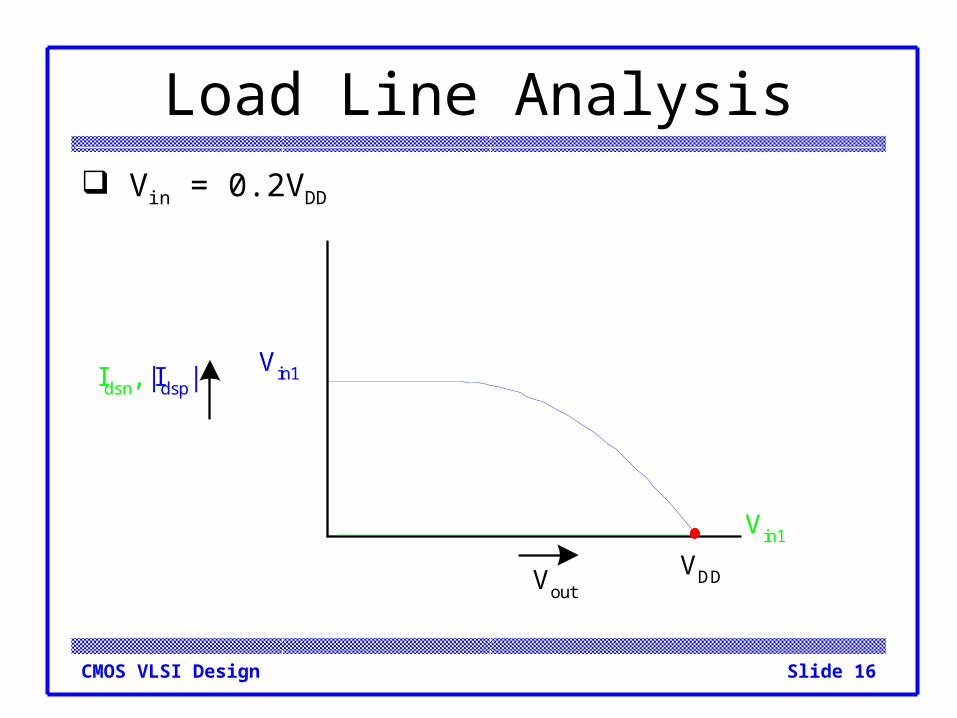
Slide 16CMOS VLSI Design
Load Line Analysis
Vin1
Vin1Idsn, |Idsp|
VoutVDD
Vin = 0.2VDD
Slide 17CMOS VLSI Design
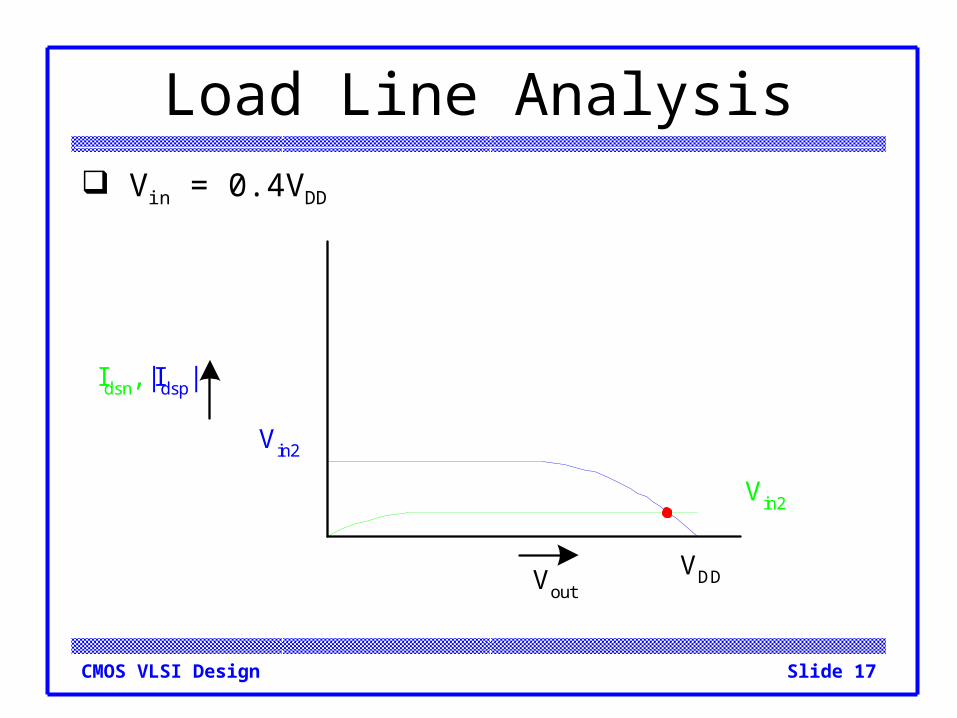
Load Line Analysis
Vin2
Vin2
Idsn, |Idsp|
VoutVDD
Vin = 0.4VDD

Slide 18CMOS VLSI Design
Load Line Analysis
Vin3
Vin3
Idsn, |Idsp|
VoutVDD
Vin = 0.6VDD

Slide 19CMOS VLSI Design
Load Line Analysis
Vin4
Vin4
Idsn, |Idsp|
VoutVDD
Vin = 0.8VDD

Slide 20CMOS VLSI Design
Load Line Analysis
Vin5Vin0
Vin1
Vin2
Vin3Vin4
Idsn, |Idsp|
VoutVDD
Vin = VDD

Slide 21CMOS VLSI Design
Load Line Summary
Vin5
Vin4
Vin3
Vin2Vin1
Vin0
Vin1
Vin2
Vin3Vin4
Idsn, |Idsp|
VoutVDD
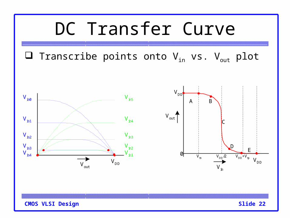
Slide 22CMOS VLSI Design
DC Transfer Curve Transcribe points onto Vin vs. Vout plot
Vin5
Vin4
Vin3
Vin2Vin1
Vin0
Vin1
Vin2
Vin3Vin4
VoutVDD
CVout
0
Vin
VDD
VDD
A B
DE
Vtn VDD/2 VDD+Vtp

Slide 23CMOS VLSI Design
Operating Regions Revisit transistor operating regions
CVout
0
Vin
VDD
VDD
A B
DE
Vtn VDD/2 VDD+Vtp
Region nMOS pMOS
A
B
C
D
E

Slide 24CMOS VLSI Design
Operating Regions Revisit transistor operating regions
CVout
0
Vin
VDD
VDD
A B
DE
Vtn VDD/2 VDD+Vtp
Region nMOS pMOS
A Cutoff Linear
B Saturation Linear
C Saturation Saturation
D Linear Saturation
E Linear Cutoff
Slide 25CMOS VLSI Design
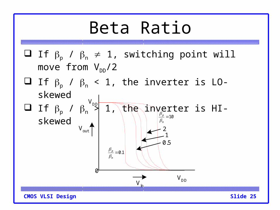
Beta Ratio If p / n 1, switching point will move from VDD/2
If p / n < 1, the inverter is LO-skewed
If p / n > 1, the inverter is HI-skewed
Vout
0
Vin
VDD
VDD
0.51
2
10p
n
0.1p
n

Slide 26CMOS VLSI Design
Noise Margins How much noise can a gate input see before it does
not recognize the input?
IndeterminateRegion
NML
NMH
Input CharacteristicsOutput Characteristics
VOH
VDD
VOL
GND
VIH
VIL
Logical HighInput Range
Logical LowInput Range
Logical HighOutput Range
Logical LowOutput Range
NMH= VOH-VIH
NML = VIL - VOL

Slide 27CMOS VLSI Design
Logic Levels To maximize noise margins, select logic levels at
VDD
Vin
Vout
VDD
p/n > 1
Vin Vout
0

Slide 28CMOS VLSI Design
Logic Levels To maximize noise margins, select logic levels at
– unity gain point of DC transfer characteristic
VDD
Vin
Vout
VOH
VDD
VOL
VIL VIHVtn
Unity Gain PointsSlope = -1
VDD-|Vtp|
p/n > 1
Vin Vout
0
Slide 29CMOS VLSI Design
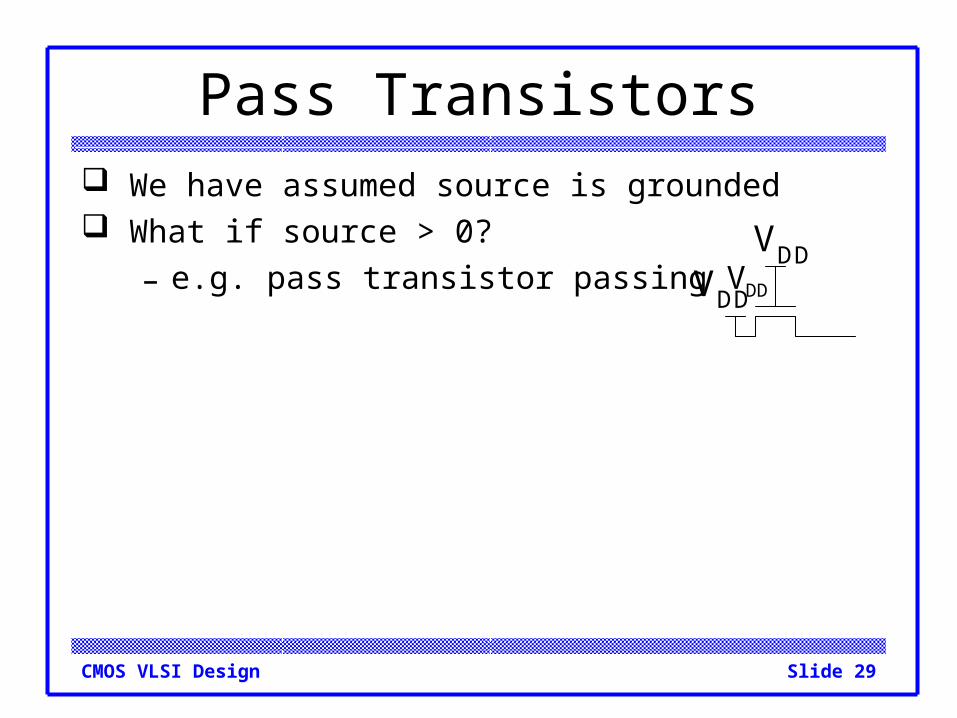
Pass Transistors We have assumed source is grounded What if source > 0?
– e.g. pass transistor passing VDD
VDDVDD

Slide 30CMOS VLSI Design
Pass Transistors We have assumed source is grounded What if source > 0?
– e.g. pass transistor passing VDD
Vg = VDD
– If Vs > VDD-Vt, Vgs < Vt
– Hence transistor would turn itself off nMOS pass transistors pull no higher than VDD-Vtn
– Called a degraded “1”
– Approach degraded value slowly (low Ids)
pMOS pass transistors pull no lower than Vtp
VDDVDD

Slide 31CMOS VLSI Design
Pass Transistor Ckts
VDDVDD
VSS
VDD
VDD
VDD VDD VDD
VDD

Slide 32CMOS VLSI Design
Pass Transistor Ckts
VDDVDD Vs = VDD-Vtn
VSS
Vs = |Vtp|
VDD
VDD-Vtn VDD-Vtn
VDD-Vtn
VDD
VDD VDD VDD
VDD
VDD-Vtn
VDD-2Vtn

Slide 33CMOS VLSI Design

Slide 34CMOS VLSI Design
Tristate Inverter
Why (d) is a bad design?
If EN = 0, Y is supposed to be float, but if A changes, charge at internal node may disturb node Y. more in section 6.3.4)

Slide 35CMOS VLSI Design
Effective Resistance Shockley models have limited value
– Not accurate enough for modern transistors– Too complicated for much hand analysis
Simplification: treat transistor as resistor
– Replace Ids(Vds, Vgs) with effective resistance R
– Ids = Vds/R
– R averaged across switching of digital gate Too inaccurate to predict current at any given time
– But good enough to predict RC delay

Slide 36CMOS VLSI Design

Slide 37CMOS VLSI Design
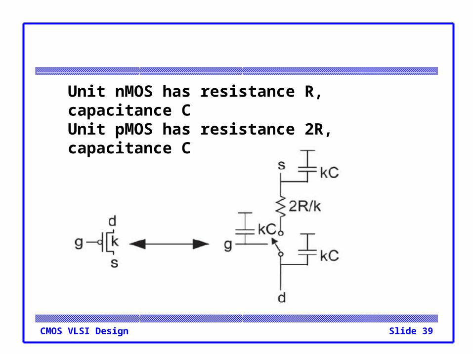
RC Delay Model Use equivalent circuits for MOS transistors
– Ideal switch + capacitance and ON resistance– Unit nMOS has resistance R, capacitance C– Unit pMOS has resistance 2R, capacitance C
Capacitance proportional to width Resistance inversely proportional to width
kg
s
d
g
s
d
kCkC
kCR/k
kg
s
d
g
s
d
kC
kC
kC
2R/k

Slide 38CMOS VLSI Design
A nMOS transistor of unit size: minimum length and minimum contacted diffusion width, size = 1 means that W = 4 , L = 2 , W/L = 2
A nMOS transistor size = k
Slide 39CMOS VLSI Design
Unit nMOS has resistance R, capacitance CUnit pMOS has resistance 2R, capacitance C

Slide 40CMOS VLSI Design
RC Values Capacitance
– C = Cg = Cs = Cd = 2 fF/m of gate width
– Values similar across many processes Resistance
– R 6 K/m in 0.6um process– Improves with shorter channel lengths
Unit transistors– May refer to minimum contacted device (4/2 )– Or maybe 1 m wide device– Doesn’t matter as long as you are consistent

Slide 41CMOS VLSI Design
Inverter Delay Estimate Estimate the delay of a fanout-of-1 inverter
2
1A
Y 2
1

Slide 42CMOS VLSI Design
Inverter Delay Estimate Estimate the delay of a fanout-of-1 inverter
C
CR
2C
2C
R
2
1A
Y
C
2C
Y2
1

Slide 43CMOS VLSI Design
Inverter Delay Estimate Estimate the delay of a fanout-of-1 inverter
C
CR
2C
2C
R
2
1A
Y
C
2C
C
2C
C
2C
RY
2
1

Slide 44CMOS VLSI Design
Inverter Delay Estimate Estimate the delay of a fanout-of-1 inverter
C
CR
2C
2C
R
2
1A
Y
C
2C
C
2C
C
2C
RY
2
1
d = 6RC