CMOS Force Sensor with Scanning Signal Process Circuit for...
18
3 CMOS Force Sensor with Scanning Signal Process Circuit for Vertical Probe Card Jung-Tang Huang, Kuo-Yu Lee and Ming-Chieh Chiu National Taipei University of Technology Taiwan 1. Introduction The constant advancement of semiconductor technology has prompted a further reduction in size and an increase in the density of integrated circuits. In order to meet the various requirements of the industry, higher accuracy, longer fatigue life, and a greater capability to withstand temperature extremes have become important criteria in the design of probe cards (Iscoff, 1994; Gilg, 1997). After a certain period of use, probe cards must be calibrated by a professional machine; several properties need to be verified, such as the probe’s maximum current, resistivity (contact resistance), and reaction force. This verification procedure may influence the efficiency of production lines, since it is performed offline. One crucial step in this procedure is monitoring the reaction force exerted by the probes on each other, in order to compute the average reaction force and complete coplanarity to ensure the efficient operation of the probe cards. To expedite this procedure, we designed an array- type CMOS force sensor that is capable of monitoring the status of vertical probe cards online in both die-level and wafer-level applications. In the past, the fabrication of pressure sensors typically involved an MEMS process with backside etching adopted for its post process (Ghalichechian, 2002; Malhair & Barbier, 2003). However, in recent years, more and more researchers have proposed to combining the standard CMOS process with the MEMS process to manufacture both microsensors and integrated circuits (Yang et al., 2005; Peng et al., 2005; Wang et al., 2006). The combined process also has additional advantages, such as a reduction in the noise and number of pads. Our design also adopted the combined CMOS-MEMS process to fabricate force sensors and their signal conditioning circuits. Moreover, as the conventional post process can barely handle the increasingly smaller pitch between the probes (Wilson, 1999), we etched a cavity on the silicon substrate to deform the membrane in the post process (RLS dry etching). 2. Design principle The main structure of a piezoresistive pressure sensor is the sensor membrane, which is made from a material that has a piezoresistance effect. As a pressure or force is exerted upon the membrane, the membrane is deformed; the piezoresistance value or resistance of the piezoresistive material changes with the stress; this is referred to as the piezoresistance effect (See Ch.2.1). The resistive materials of the sensor are then connected to a Wheatstone Open Access Database www.intechweb.org Source: Sensors, Focus on Tactile, Force and Stress Sensors, Book edited by: Jose Gerardo Rocha and Senentxu Lanceros-Mendez, ISBN 978-953-7619-31-2, pp. 444, December 2008, I-Tech, Vienna, Austria www.intechopen.com
Transcript of CMOS Force Sensor with Scanning Signal Process Circuit for...

3
CMOS Force Sensor with Scanning Signal Process Circuit for Vertical Probe Card
Jung-Tang Huang, Kuo-Yu Lee and Ming-Chieh Chiu National Taipei University of Technology
Taiwan
1. Introduction
The constant advancement of semiconductor technology has prompted a further reduction in size and an increase in the density of integrated circuits. In order to meet the various requirements of the industry, higher accuracy, longer fatigue life, and a greater capability to withstand temperature extremes have become important criteria in the design of probe cards (Iscoff, 1994; Gilg, 1997). After a certain period of use, probe cards must be calibrated by a professional machine; several properties need to be verified, such as the probe’s maximum current, resistivity (contact resistance), and reaction force. This verification procedure may influence the efficiency of production lines, since it is performed offline. One crucial step in this procedure is monitoring the reaction force exerted by the probes on each other, in order to compute the average reaction force and complete coplanarity to ensure the efficient operation of the probe cards. To expedite this procedure, we designed an array-type CMOS force sensor that is capable of monitoring the status of vertical probe cards online in both die-level and wafer-level applications. In the past, the fabrication of pressure sensors typically involved an MEMS process with backside etching adopted for its post process (Ghalichechian, 2002; Malhair & Barbier, 2003). However, in recent years, more and more researchers have proposed to combining the standard CMOS process with the MEMS process to manufacture both microsensors and integrated circuits (Yang et al., 2005; Peng et al., 2005; Wang et al., 2006). The combined process also has additional advantages, such as a reduction in the noise and number of pads. Our design also adopted the combined CMOS-MEMS process to fabricate force sensors and their signal conditioning circuits. Moreover, as the conventional post process can barely handle the increasingly smaller pitch between the probes (Wilson, 1999), we etched a cavity on the silicon substrate to deform the membrane in the post process (RLS dry etching).
2. Design principle
The main structure of a piezoresistive pressure sensor is the sensor membrane, which is made from a material that has a piezoresistance effect. As a pressure or force is exerted upon the membrane, the membrane is deformed; the piezoresistance value or resistance of the piezoresistive material changes with the stress; this is referred to as the piezoresistance effect (See Ch.2.1). The resistive materials of the sensor are then connected to a Wheatstone O
pen
Acc
ess
Dat
abas
e w
ww
.inte
chw
eb.o
rg
Source: Sensors, Focus on Tactile, Force and Stress Sensors, Book edited by: Jose Gerardo Rocha and Senentxu Lanceros-Mendez, ISBN 978-953-7619-31-2, pp. 444, December 2008, I-Tech, Vienna, Austria
www.intechopen.com

Sensors, Focus on Tactile, Force and Stress Sensors
38
bridge to enhance their sensitivity. Thus, with the help of the Wheatstone bridge, we can obtain the value of ΔV when the resistance values changes. The resistance and ΔV values vary greatly as the pressure increases (See Ch.2.2). The pressure can be measured on the basis of the output value of ΔV once the relation between the pressure and ΔV is established.
2.1 Piezoresistance effect In 1856, Lord Kelvin discovered the phenomenon of the piezoresistance effect. However, the practicality of the principle was only applied to a strain gauge in 1939, with metal used for the strain gauge material. Strain gauges are now used in many measurement applications, such as for mechanisms, buildings, airplanes, and scales. But, the resistance change rate for a metal strain gauge is very small. As a result, in applications that require the detection of small amounts of strain, metal strain gauges do not provide a sufficient sensitivity or signal/noise ratio. In 1954, Smith first exerted stress in the axial direction on a shaft that had been doped with silicon and germanium, and then measured the change rate of the resistance in the vertical direction (Smith, 1954). The physical relationship between the resistance and stress is first established. The principle and architecture of a piezoresistive pressure sensor is as shown below (Petersen, 1982; Thurston, 1964):
VR
RP Δ⇒Δ⇒⇒⇒⇒Δ σεω (1)
where ΔP is the change in the pressure; ω, the membrane deformation; ε, strain; σ, stress; ΔR /R, ratio of variation; and ΔV, potential difference. And the change rate of the resistance is:
( ) ρρνε Δ++=Δ
21R
R (2)
where ┥ is Poisson’s ratio, Δ┩/┩ is the change rate of resistivity, (1+2┥) is the deformation of the material by the external pressure. Since silicon has a square structure, the relationship between the change rate of resistivity and the stress can be simply shown in the following matrix equation:
⎟⎟⎟⎟⎟⎟⎟⎟
⎠
⎞
⎜⎜⎜⎜⎜⎜⎜⎜
⎝
⎛
⎟⎟⎟⎟⎟⎟⎟⎟
⎠
⎞
⎜⎜⎜⎜⎜⎜⎜⎜
⎝
⎛
=
⎟⎟⎟⎟⎟⎟⎟⎟
⎠
⎞
⎜⎜⎜⎜⎜⎜⎜⎜
⎝
⎛
ΔΔΔΔΔΔ
Δ
3
2
1
3
2
1
44
44
44
111212
121112
121211
6
5
4
3
2
1
00000
00000
00000
000
000
000
1
τττσσσ
ππ
ππππππππππ
ρρρρρρ
ρ (3)
For the function, [┨] is the coefficient for the piezoresistance matrix. The material characteristics and coefficient for the piezoresistance matrix can be simply converted by Euler coordinates into the following equation:
])[(2
2
2
1
2
1
2
1
2
2
2
144121111nnmmll
T++−−+= πππππ (4)
])[(22
1
2
1
2
1
2
1
2
1
2
144121111 nlnmmlL
++−−−= πππππ (5)
www.intechopen.com

CMOS Force Sensor with Scanning Signal Process Circuit for Vertical Probe Card
39
where l1, m1, n1, l2, m2, and n2 are the transverse direction cosine and longitudinal direction cosine, respectively (Kanda, 1982). The relationship between the change rate of the resistance and the stress can be simply shown in the following equation:
TTLL
R
R σπσπρρ +=Δ=Δ (6)
where σL and σT are the longitudinal stress and transverse stress, and ┨L and ┨T are the longitudinal piezoresistance coefficient and transverse piezoresistance coefficient, respectively.
2.2 The Wheatstone bridge principle Piezoresistive pressure sensors use piezoresistive materials embedded in the membrane of the sensor, and adopt the Wheatstone bridge principle, as shown in Fig. 1. Four piezoresistances are placed at the edge of a square membrane (two transverse piezoresistances; two longitudinal piezoresistances). The transverse and longitudinal piezoresistances are influenced by stress when the membrane deforms. The transverse piezoresistances will be widened and reduced, while the other piezoresistances will be lengthened and increased.
Fig. 1. The circuit structure of Wheatstone bridge.
The relationship between the output and input voltage is shown in the following equation:
43
4
21
2
RR
R
RR
R
V
V
IN
OUT +−+= (7)
When the resistances do not change, the output voltage is zero.
R1=R2=R3=R4=R, VOUT=0 (8)
When pressure is exerted upon the sensor, the resistances will change in an ideal situation:
R2= R3=R+ΔR瑑 R1= R4=R-ΔR (9)
www.intechopen.com

Sensors, Focus on Tactile, Force and Stress Sensors
40
Thus, the relationship between the output voltage and exerted pressure can be established:
kPR
R
V
V
in
out =Δ=
(10)
Therefore, the situation assumes elasticity:
P
R
R ∝Δ (11)
As seen in the above equation, we can utilize the change rate of the output voltage to
evaluate the change rate of the resistances and thus obtain a pressure measurement.
3. Design and fabrication
First, sensor loading and other properties were simulated. If the properties of the sensor
conformed to our requests, a photo mask for the sensor was designed. Then, we adopted the
TSMC standard process and the post process (RLS) by CIC. The last step was packaging and
measurement.
3.1 Simulation of sensor There were two parts to the CMOS force sensor simulation: the membrane structure and
the piezoresistance locations. The force range of a normal vertical probe card is about 3g ~
5g, according to a previous reference (Gilg, 1997). Table 1. summarizes the properties of
the main materials used in the IC fabrication process for the initial design. The optimal
membrane area could be determined based on the probe pitch and membrane depth. The
simulation parameter settings are shown in Fig. 2. These include (a) Force: Since the force
range of a normal vertical probe card is about 3g ~ 5g, the force range for the simulation
was set at 0g ~ 5g, and (b) Boundary condition: The edge of the sensor membrane was
firmly fixed. However, since only pressure could be set in the simulation software
(CoventorWare), we needed to convert force to pressure (0 MPa ~ 60 MPa) for the
simulation.
Property Material
Yield stress (GPa) Young's modulus
(GPa) Poisson ratio
Silicon dioxide 8.4 73 0.17
Silicon 7.0 190 0.23
Polysilicon 2.7 140 0.2
Nitride 14.0 260 0.27
Tungsten 4.0 410 0.28
Aluminum 0.17 70 0.35
Table 1. The property of materials in the TSMC standard process [9]
www.intechopen.com

CMOS Force Sensor with Scanning Signal Process Circuit for Vertical Probe Card
41
Fig. 2. The setting of boundary condition with the membrane of sensor in our simulation
3.1.1 Simulation of membrane structure Table 1. summarizes the properties of the main materials used in the IC fabrication process, based on the limits of the TSMC .35 2P4M process. Among these materials, silicon dioxide and metal are the best membrane materials because their Young’s modulus and yield stresses are good. In addition, we also considered the probe diameter (40 x 40 ┤m2) when assembling a vertical probe card, designing the membrane area to be 100 x 100 ┤m2. Fig. 3
(a) (b) Fig. 3. The pressure as 65MPa (a) Distribution of the von Mises stress of the COMS force sensor. (b) Distribution of the deformation of the COMS force sensor.
www.intechopen.com

Sensors, Focus on Tactile, Force and Stress Sensors
42
shows a distribution map for the von Mises stress when the membrane was compressed by
an external pressure. We were able to resolve the loading range for the force sensor after
determining a 100 x 100 ┤m2 area for the membrane. When more metal layers were
employed, the structural strength was weaker; when more silicon dioxide layers were
employed there was less deformation. For a trade-off between the strength of the membrane
structure and the sensitivity of the piezoresistance, we decided to use a membrane structure
composed of two metal layers and two silicon dioxide layers. The main membrane material
was silicon dioxide, which had a yield stress of 8.4 Gpa, as shown in Table A. According to
the simulation results, the von Mises stress over the yield stress when the loading force is
65MPa on the membrane. Therefore, the optimum loading range of the force sensor was 0 to
5 grams (100 x 100 ┤m2; the safety factor was 2 to 3).
3.1.2 Simulation of piezoresistive location Based on the simulation results (see Fig. 4) and a previous study (Ghalichechian, 2002), the
maximum stress was at the edge of the membrane. Therefore, the piezoresistance was
placed at the edge of the membrane to measure the maximum membrane strain. The
resistance change rate and sensor sensitivity increased simultaneously. The initial design
adopted the traditional type of piezoresistance (rectangular and sheet piezoresistance) for
the simulation, and the current density was 14 nA/┤m2, as shown in Fig. 5. The current was
sparse at the corners, so we beveled them (45°). The density of the current then rose to 24
nA/┤m2, as shown in Fig. 6. The altered design could improve the resistance change rate
and raise the sensitivity of the sensor. After deciding on the piezoresistance shape, we
moved the piezoresistance to the center of the membrane from its central edge. The
maximum current for the transverse piezoresistance was found at 17 µm, as shown in Fig.
7(a). The maximum current for the longitudinal piezoresistance was found at 2, 3, 9 and 18
µm, as shown in Fig. 7(b).
(a) (b)
Fig. 4. Distribution of the von Mises stress of the COMS force sensor (size 100┤m2) when the pressure as 65MPa. (a) XX-direction. (b) YY-direction.
www.intechopen.com

CMOS Force Sensor with Scanning Signal Process Circuit for Vertical Probe Card
43
(a) (b)
Fig. 5. (a) The traditional transverse piezoresistance. (b) The traditional longitudinal piezoresistance.
(a) (b)
Fig. 6. (a) The bevel transverse piezoresistance. (b) The bevel longitudinal piezoresistance.
(a) (b)
Fig. 7. (a) The change chart of current when the transverse piezoresistance moves to the center of membrane. (b) The change chart of current when the longitudinal piezoresistance moves to the center of membrane.
www.intechopen.com
Sensors, Focus on Tactile, Force and Stress Sensors
44
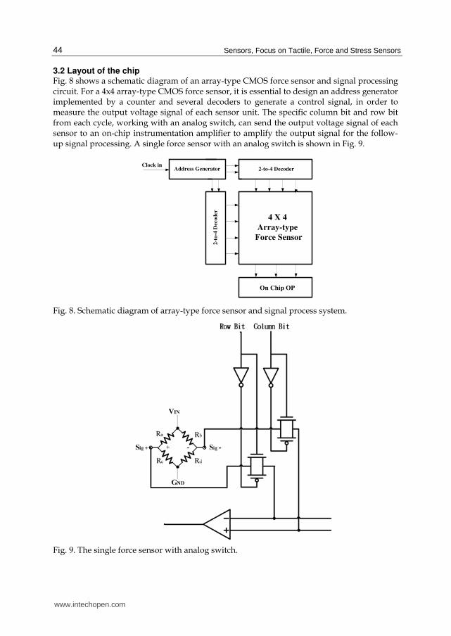
3.2 Layout of the chip Fig. 8 shows a schematic diagram of an array-type CMOS force sensor and signal processing circuit. For a 4x4 array-type CMOS force sensor, it is essential to design an address generator implemented by a counter and several decoders to generate a control signal, in order to measure the output voltage signal of each sensor unit. The specific column bit and row bit from each cycle, working with an analog switch, can send the output voltage signal of each sensor to an on-chip instrumentation amplifier to amplify the output signal for the follow-up signal processing. A single force sensor with an analog switch is shown in Fig. 9.
2-to-4 Decoder
2-t
o-4
Deco
der
4 X 4
Array-type
Force Sensor
On Chip OP
Address GeneratorClock in
Fig. 8. Schematic diagram of array-type force sensor and signal process system.
Fig. 9. The single force sensor with analog switch.
www.intechopen.com

CMOS Force Sensor with Scanning Signal Process Circuit for Vertical Probe Card
45
The chip had sixteen force sensors, and many pads around the sensors, as shown in Fig. 10. In order to match the probe distances of our vertical probe card, the central distance of each force sensor was designed to be 250 µm. A pad was then opened on the top of each sensor for measuring the probe signal. So, the sensor could simultaneously measure the probe signal and the force sensor signal.
Fig. 10. The layout of array-type CMOS force sensor.
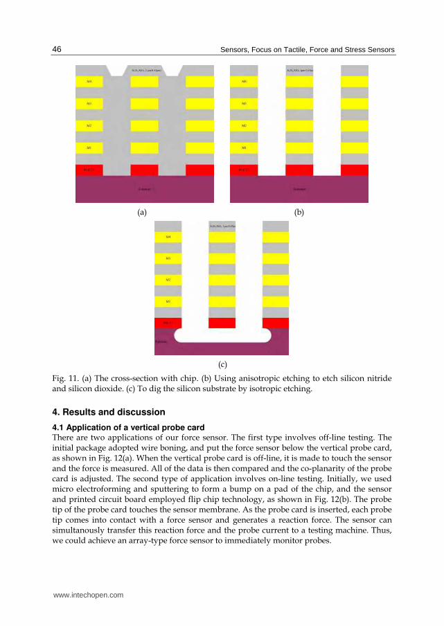
3.3 Process of fabrication After it was verified that the simulation met the design requirements, the design was drafted and a design rule check (DRC) was performed. The standard TSMC 0.35 µm 2P4M process offered by the Chip Implementation Center (CIC, 2008) was then adopted to fabricate the sensor. Fig. 11(a) shows a cross section of the fabricated chip. Further, we employed a post process (RLS dry etching) supplied by CIC (CIC, 2008). The first step in the process involved the anisotropic etching of silicon nitride and silicon dioxide, as shown in Fig. 11(b). The next step was to etch the silicon substrate by isotropic etching, as shown in Fig. 11(c).
3.4 Piezoresistance Actually, there are two types of piezoresistance in polycrystalline silicon: p+ and n+, which have well known piezoresistance effects (the gauge factor is 30 (French, 2002; Seto, 1976)). We adopted polycrystalline silicon (poly1 layer n+) in the design of the sensor’s piezoresistance. The reason for adopting the poly1 layer is that it is located at the bottommost layer of the membrane. Therefore, the largest thickness can be used for the membrane structure. In addition, the resistivity (┩) of the poly1 layer is 0.85 mΩ-cm, based on the data offered by CIC.
www.intechopen.com
Sensors, Focus on Tactile, Force and Stress Sensors
46
(a) (b)
(c)
Fig. 11. (a) The cross-section with chip. (b) Using anisotropic etching to etch silicon nitride and silicon dioxide. (c) To dig the silicon substrate by isotropic etching.
4. Results and discussion
4.1 Application of a vertical probe card There are two applications of our force sensor. The first type involves off-line testing. The initial package adopted wire boning, and put the force sensor below the vertical probe card, as shown in Fig. 12(a). When the vertical probe card is off-line, it is made to touch the sensor and the force is measured. All of the data is then compared and the co-planarity of the probe card is adjusted. The second type of application involves on-line testing. Initially, we used micro electroforming and sputtering to form a bump on a pad of the chip, and the sensor and printed circuit board employed flip chip technology, as shown in Fig. 12(b). The probe tip of the probe card touches the sensor membrane. As the probe card is inserted, each probe tip comes into contact with a force sensor and generates a reaction force. The sensor can simultanously transfer this reaction force and the probe current to a testing machine. Thus, we could achieve an array-type force sensor to immediately monitor probes.
www.intechopen.com

CMOS Force Sensor with Scanning Signal Process Circuit for Vertical Probe Card
47
(a)
(b)
Fig. 12. The cross-sectional view of the vertical probe card with CMOS force sensor (a) off-line (b) on-line
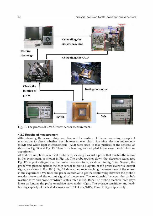
4.2 CMOS force sensor measurement Fig. 13 illustrates the measurement process for the CMOS force sensor. First, commands
were entered into a computer to control a six-axis precision instrument by means of
programs and a multi-axis controller. Secondly, an apparatus with a probe was fabricated to
compress the sensor chip, and a charge coupled device (CCD) was used to observe whether
the probe was able to establish precise contact with the sensor. Finally, for the four
resistances of the sensor’s Wheatstone bridge, the two input points were connected to a
power supply, and both the output points were connected to an oscilloscope.
www.intechopen.com
Sensors, Focus on Tactile, Force and Stress Sensors
48
Fig. 13. The process of CMOS forces sensor measurement.
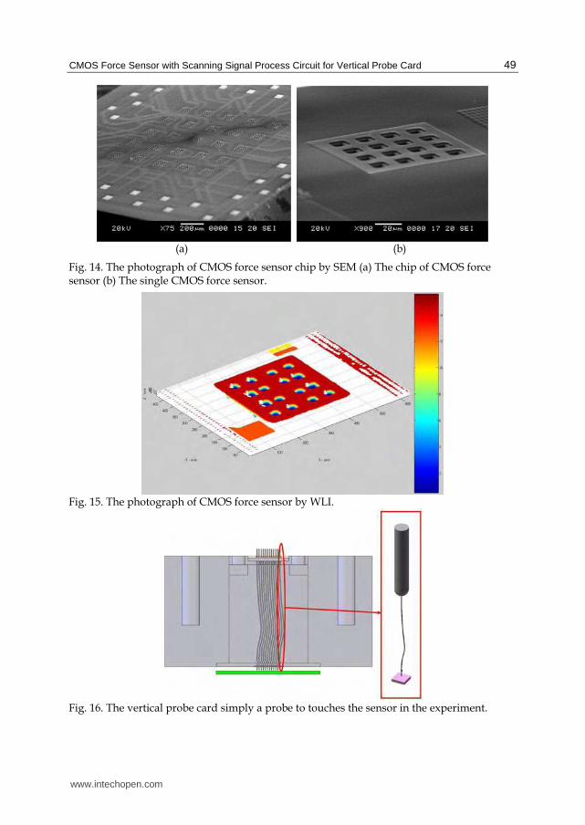
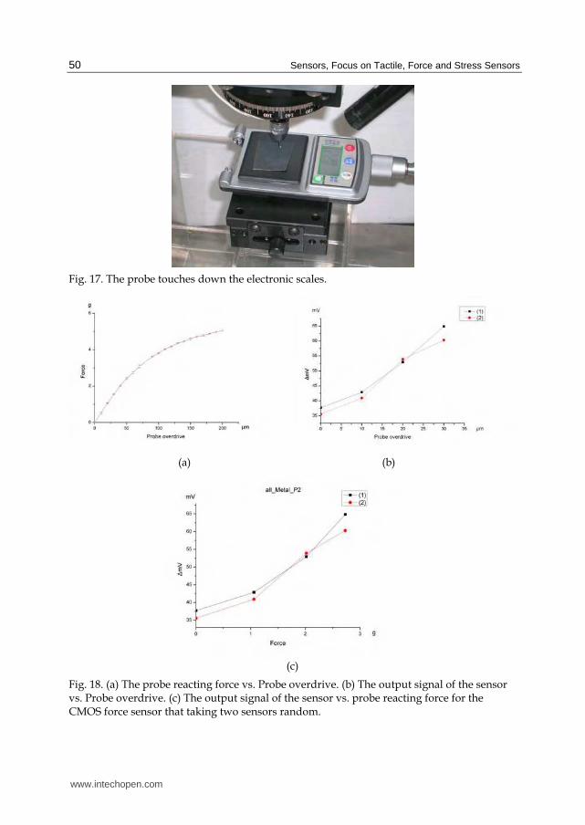
4.2.2 Results of measurement After cleaning the sensor chip, we observed the surface of the sensor using an optical microscope to check whether the photoresist was clean. Scanning electron microscopy (SEM) and white light interferometers (WLI) were used to take pictures of the sensors, as shown in Fig. 14 and Fig. 15. Then, wire bonding was adopted to package the chip for our experiment. At first, we simplified a vertical probe card, viewing it as just a probe that touches the sensor in the experiment, as shown in Fig. 16. The probe touches down the electronic scales (see Fig. 17) to plot a diagram of the probe overdrive force, as shown in Fig. 18(a). Second, the probe was pushed against the chip sensor to plot a diagram of the probe overdrive-output signal, as shown in Fig. 18(b). Fig. 19 shows the probe touching the membrane of the sensor in the experiment. We fixed the probe overdrive to get the relationship between the probe’s reaction force and the output signal of the sensor. The relationship between the probe’s reaction force and probe overdrive is illustrated in Fig. 18(c). The probe’s reaction force stays linear as long as the probe overdrive stays within 40µm. The average sensitivity and load-bearing capacity of the tested sensors were 3.114 mV/MPa/V and 0~3 g, respectively.
www.intechopen.com
CMOS Force Sensor with Scanning Signal Process Circuit for Vertical Probe Card
49
(a) (b)
Fig. 14. The photograph of CMOS force sensor chip by SEM (a) The chip of CMOS force sensor (b) The single CMOS force sensor.
Fig. 15. The photograph of CMOS force sensor by WLI.
Fig. 16. The vertical probe card simply a probe to touches the sensor in the experiment.
www.intechopen.com
Sensors, Focus on Tactile, Force and Stress Sensors
50
Fig. 17. The probe touches down the electronic scales.
(a) (b)
(c)
Fig. 18. (a) The probe reacting force vs. Probe overdrive. (b) The output signal of the sensor vs. Probe overdrive. (c) The output signal of the sensor vs. probe reacting force for the CMOS force sensor that taking two sensors random.
www.intechopen.com

CMOS Force Sensor with Scanning Signal Process Circuit for Vertical Probe Card
51
(a) (b)
Fig. 19. The probe tip touches down the membrane of sensor (a) actual experiment (b) CCD camera.
5. Conclusion
Probe cards play an extremely important role in the semiconductor industry. In this study, we designed a CMOS piezoresistive force sensor to be applied to the probe cards. Capable of simultaneously monitoring the probe reacting force and electrical signals, the designed sensor can help operators immediately identify a broken or a deformed probe and recognize that the received signals are erroneous. The repair time and cost of the probes can therefore be reduced. Further, we adopted the TSMC 0.35 µm 2P4M process to fabricate the CMOS force sensor that can be integrated with the circuit. According to the measurement results, the designed sensor reports an average sensitivity of 3.114 mV/MPa/V and a load-bearing capacity ranging from 0 to 3 g.
6. Acknowledgements
The author would like to thank C.C.P. Contact Probes Co., Ltd. for their help. We also thank the Chip Implementation Center of the National Science Council, Taiwan, R.O.C., for supporting the TSMC 0.35um CMOS process. The fund is granted from NSC 94-2622-E-027 -047 -CC3.
7. References
Iscoff, R. (1994). What’s in the cards for wafer probing, Semiconductor. Int., June 1994, pp. 76 Gilg, L. (1997). Know good die, Journal of Electronic Testing: Theory and Applications, vol.
10, issue 1-2, April 1997, pp. 2019, ISSN:0923-8174 Ghalichechian, N.; Khbeis, M.; Ma, Z.; Moghadam, S. & Tan X. (2002). Piezo-resistor
pressure sensor cluster, ENEE605 Final Project Report, Fall 2002 Department of Electrical and Computer Engineering Group #2, University of Maryland
Malhair, C. & Barbier, D. (2003). Design of a polysilicon-on-insulator pressure sensor with original polysilicon layout for harsh environment," Thin Solid Films, vol. 427, issues 1-2, 3 March 2003, pp. 362-366, ISSN 0040-6090
www.intechopen.com

Sensors, Focus on Tactile, Force and Stress Sensors
52
Yang, L. J.; Lai, C. C.; Dai, C. L. & Chang, P. Z. (2005). A piezoresistive micro pressure sensor fabricated by commercial DPDM CMOS process, Tamkang Journal of Science and Engineering, vol. 8, no. 1, 2005, pp. 67-73
Peng, C. T.; Lin, J. C.; Lin C. T. & Chiang, K. N. (2005). Performance and package effect of a novel piezoresistive pressure sensor fabricated by front–side etching technology, Sensors and Actuators A: Physical, vol. 119, 2005, pp. 28-37, ISSN 0924-4247
Wang, H. H. & Yang, L. J. (2006). Micro pressure sensors of 50┤m size fabricated by a standard CMOS foundry and a novel post process, MEMS 2006, pp. 22-26, Turkey, 22-26 January, Istanbul
Wilson, L. (1999). The National Technology Roadmap for Semiconductor, Semiconductor Industry Association, San Jose, California, November, 1999
Smith, C. S. (1954). Piezoresistance effect in germanium and silicon, Physical Review, vol. 94, issue 1, April 1954, pp. 42-49
Petersen, K. E. (1982). Silicon as a Mechanical Material" Proceedings of The IEEE., vol. 70, no. 5, May 1982, pp. 420-457
Thurston, R. N. (1964). Use of semiconductor transducers in measuring strain, accelerations, and displacements, Physical Acoustics, vol. 1, pt. B. New York: Academic Press, 1964, pp. 215-235
Kanda, Y. (1982). A graphical representation of the piezoresistance coefficients in silicon, IEEE Transactions on Electron Devices, vol. ED-29, no. 1, January, pp. 64-70
French, P. J. (2002). Polysilicon瑍a versatile material for microsystems, Sensors and Actuators A: Physical, vol. 99, 20 January 2002, pp. 3-12
The CIC CMOS MEMS Design Platform for Heterogeneous Integration, Chip Implementation Center, CIC, Taiwan, Document no. CIC-CID-RD-08-01, April 2008
Seto, J. Y. W. (1976). Piezoresistive properties of polycrystalline silicon, Journal of Applied Physics, vol. 47, no. 11, November 1976, pp.4780-4783
www.intechopen.com
Sensors: Focus on Tactile Force and Stress SensorsEdited by Jose Gerardo Rocha and Senentxu Lanceros-Mendez
ISBN 978-953-7619-31-2Hard cover, 444 pagesPublisher InTechPublished online 01, December, 2008Published in print edition December, 2008
InTech EuropeUniversity Campus STeP Ri Slavka Krautzeka 83/A 51000 Rijeka, Croatia Phone: +385 (51) 770 447 Fax: +385 (51) 686 166www.intechopen.com
InTech ChinaUnit 405, Office Block, Hotel Equatorial Shanghai No.65, Yan An Road (West), Shanghai, 200040, China
Phone: +86-21-62489820 Fax: +86-21-62489821
This book describes some devices that are commonly identified as tactile or force sensors. This is achievedwith different degrees of detail, in a unique and actual resource, through the description of differentapproaches to this type of sensors. Understanding the design and the working principles of the sensorsdescribed here requires a multidisciplinary background of electrical engineering, mechanical engineering,physics, biology, etc. An attempt has been made to place side by side the most pertinent information in orderto reach a more productive reading not only for professionals dedicated to the design of tactile sensors, butalso for all other sensor users, as for example, in the field of robotics. The latest technologies presented in thisbook are more focused on information readout and processing: as new materials, micro and sub-microsensors are available, wireless transmission and processing of the sensorial information, as well as someinnovative methodologies for obtaining and interpreting tactile information are also strongly evolving.
How to referenceIn order to correctly reference this scholarly work, feel free to copy and paste the following:
Jung-Tang Huang, Kuo-Yu Lee and Ming-Chieh Chiu (2008). CMOS Force Sensor with Scanning SignalProcess Circuit for Vertical Probe Card, Sensors: Focus on Tactile Force and Stress Sensors, Jose GerardoRocha and Senentxu Lanceros-Mendez (Ed.), ISBN: 978-953-7619-31-2, InTech, Available from:http://www.intechopen.com/books/sensors-focus-on-tactile-force-and-stress-sensors/cmos_force_sensor_with_scanning_signal_process_circuit_for_vertical_probe_card

© 2008 The Author(s). Licensee IntechOpen. This chapter is distributedunder the terms of the Creative Commons Attribution-NonCommercial-ShareAlike-3.0 License, which permits use, distribution and reproduction fornon-commercial purposes, provided the original is properly cited andderivative works building on this content are distributed under the samelicense.