CMOS 16-BiT SinGle ChiP MiCROCOnTROlleR …Rev. 1.0 CMOS 16-BiT SinGle ChiP MiCROCOnTROlleR...
281
Rev. 1.0 CMOS 16-BIT SINGLE CHIP MICROCONTROLLER S1C17555/565/955/965 Technical Manual
Transcript of CMOS 16-BiT SinGle ChiP MiCROCOnTROlleR …Rev. 1.0 CMOS 16-BiT SinGle ChiP MiCROCOnTROlleR...

Rev. 1.0
CMOS 16-BiT SinGle ChiP MiCROCOnTROlleR
S1C17555/565/955/965Technical Manual

© SEIKO EPSON CORPORATION 2012, All rights reserved.
NOTICENo part of this material may be reproduced or duplicated in any form or by any means without the written permission of Seiko Epson. Seiko Epson reserves the right to make changes to this material without notice. Seiko Epson does not assume any liability of any kind arising out of any inaccuracies contained in this material or due to its application or use in any product or circuit and, further, there is no representation that this material is applicable to products requiring high level reliability, such as, medical prod-ucts. Moreover, no license to any intellectual property rights is granted by implication or otherwise, and there is no representation or warranty that anything made in accordance with this material will be free from any patent or copyright infringement of a third party. When exporting the products or technology described in this material, you should comply with the applicable export control laws and regulations and follow the procedures required by such laws and regulations. You are requested not to use, to resell, to export and/or to otherwise dispose of the products (and any technical information furnished, if any) for the development and/or manufacture of weapon of mass destruction or for other military purposes.
All brands or product names mentioned herein are trademarks and/or registered trademarks of their respective companies.
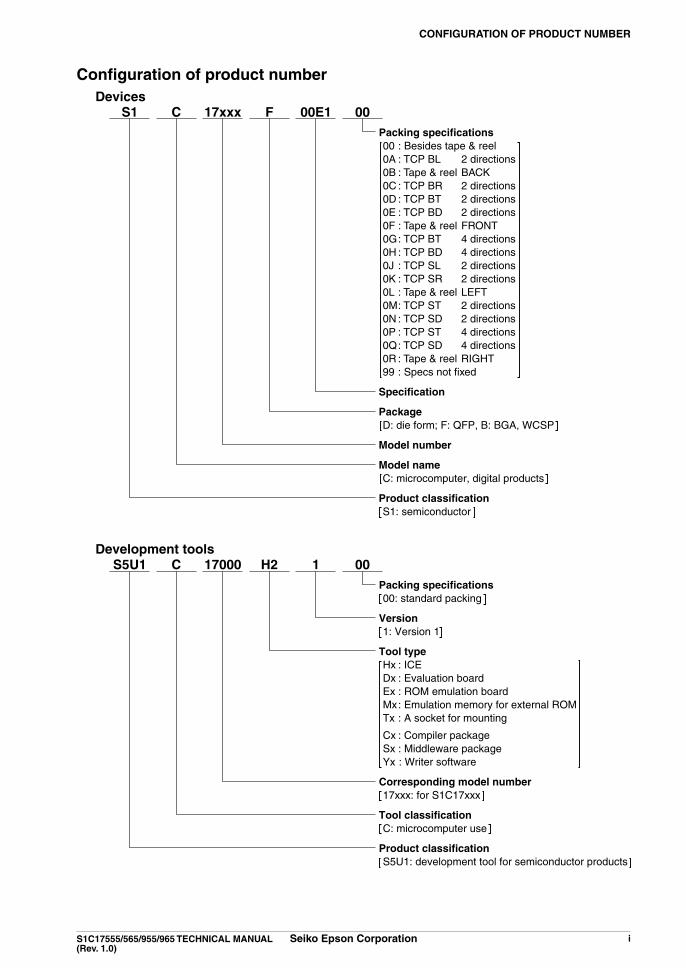
DevicesS1 C 17xxx F 00E1
Packing specifications 00 : Besides tape & reel 0A : TCP BL 2 directions 0B : Tape & reel BACK 0C : TCP BR 2 directions 0D : TCP BT 2 directions 0E : TCP BD 2 directions 0F : Tape & reel FRONT 0G : TCP BT 4 directions 0H : TCP BD 4 directions 0J : TCP SL 2 directions 0K : TCP SR 2 directions 0L : Tape & reel LEFT 0M : TCP ST 2 directions 0N : TCP SD 2 directions 0P : TCP ST 4 directions 0Q : TCP SD 4 directions 0R : Tape & reel RIGHT 99 : Specs not fixed
Specification
Package D: die form; F: QFP, B: BGA, WCSP
Model number
Model name C: microcomputer, digital products
Product classification S1: semiconductor
Development toolsS5U1 C 17000 H2 1
Packing specifications 00: standard packing
Version 1: Version 1
Tool type Hx : ICE Dx : Evaluation board Ex : ROM emulation board Mx : Emulation memory for external ROM Tx : A socket for mounting
Cx : Compiler package Sx : Middleware package Yx : Writer software
Corresponding model number 17xxx: for S1C17xxx
Tool classification C: microcomputer use
Product classification S5U1: development tool for semiconductor products
00
00
Configuration of product number
COnFiGuRaTiOn OF PRODuCT nuMBeR
S1C17555/565/955/965 TeChniCal Manual Seiko epson Corporation i(Rev. 1.0)
Configuration of product number

CONTENTS
ii Seiko epson Corporation S1C17555/565/955/965 TeChniCal Manual (Rev. 1.0)
– Contents –
1 Overview ........................................................................................................................1-11.1 Features ...........................................................................................................................1-1
1.2 Block Diagram ..................................................................................................................1-3
1.3 Pins ..................................................................................................................................1-71.3.1 S1C17555/955 Pin Configuration Diagram (WCSP-48) ....................................1-71.3.2 S1C17565/965 Pin Configuration Diagram (TQFP13-64pin) .............................1-81.3.3 S1C17565/965 Pad Configuration Diagram (Chip) ............................................1-91.3.4 Pin Descriptions ................................................................................................1-11
2 CPu ................................................................................................................................2-12.1 Features of the S1C17 Core ............................................................................................2-1
2.2 CPU Registers .................................................................................................................2-2
2.3 Instruction Set ..................................................................................................................2-2
2.4 Reading PSR ...................................................................................................................2-5
2.5 Processor Information ......................................................................................................2-6
3 Memory Map, Bus Control ...........................................................................................3-13.1 Bus Cycle .........................................................................................................................3-1
3.1.1 Restrictions on Access Size...............................................................................3-23.1.2 Restrictions on Instruction Execution Cycles .....................................................3-2
3.2 Flash Area ........................................................................................................................3-23.2.1 Embedded Flash Memory ..................................................................................3-23.2.2 Flash Programming ...........................................................................................3-23.2.3 Protect Bits ........................................................................................................3-23.2.4 Flash Memory Read Wait Cycle Setting ...........................................................3-3
FLASHC Read Wait Control Register (FLASHC_WAIT) ........................................................... 3-3
3.3 Internal RAM Area............................................................................................................3-43.3.1 Embedded RAM ................................................................................................3-4
IRAM Size Register (MISC_IRAMSZ) ....................................................................................... 3-4
3.4 Internal Peripheral Area ...................................................................................................3-5
3.5 S1C17 Core I/O Area .......................................................................................................3-5
4 Power Supply ................................................................................................................4-14.1 Core Power Supply Voltage (LVDD) ...................................................................................4-1
4.2 I/O Power Supply Voltage (HVDD) .....................................................................................4-1
4.3 Analog Power Supply Voltage (AVDD) [S1C17565/965] ....................................................4-1
4.4 Flash Programming Power Supply Voltage (VPP) .............................................................4-1
4.5 Embedded Regulators .....................................................................................................4-24.5.1 LVDD Regulator [S1C17565/965] ........................................................................4-24.5.2 AVDD Regulator [S1C17565/965] .......................................................................4-24.5.3 VPP Regulator/Booster .......................................................................................4-2
4.6 Control Register Details [S1C17565/965] ........................................................................4-3VD1 Control Register (VD1_CTL) ............................................................................................... 4-3ADC12SA2 Power Control Register (ADC12_ACTL) ................................................................ 4-3
4.7 Precautions on Power Supply ..........................................................................................4-4
5 initial Reset ...................................................................................................................5-15.1 Initial Reset Sources ........................................................................................................5-1
5.1.1 #RESET Pin .......................................................................................................5-15.1.2 P0 Port Key-Entry Reset ...................................................................................5-15.1.3 Resetting by the Watchdog Timer ......................................................................5-1

CONTENTS
S1C17555/565/955/965 TeChniCal Manual Seiko epson Corporation iii(Rev. 1.0)
5.2 Initial Reset Sequence .....................................................................................................5-2
5.3 Initial Settings After an Initial Reset ................................................................................5-2
6 interrupt Controller (iTC) .............................................................................................6-16.1 ITC Module Overview .......................................................................................................6-1
6.2 Vector Table ......................................................................................................................6-2Vector Table Address Low/High Registers (MISC_TTBRL, MISC_TTBRH) .............................. 6-4
6.3 Control of Maskable Interrupts .........................................................................................6-46.3.1 Interrupt Control Bits in Peripheral Modules ......................................................6-46.3.2 ITC Interrupt Request Processing .....................................................................6-46.3.3 Interrupt Processing by the S1C17 Core ...........................................................6-5
6.4 NMI ...................................................................................................................................6-6
6.5 Software Interrupts ...........................................................................................................6-6
6.6 HALT and SLEEP Mode Cancellation ..............................................................................6-6
6.7 Control Register Details ...................................................................................................6-6Interrupt Level Setup Register x (ITC_LVx) ............................................................................... 6-7
7 Clock Generator (ClG) .................................................................................................7-17.1 CLG Module Overview .....................................................................................................7-1
7.2 CLG Input/Output Pins .....................................................................................................7-2
7.3 Oscillators ........................................................................................................................7-27.3.1 IOSC Oscillator ..................................................................................................7-27.3.2 OSC3 Oscillator [S1C17565/965] ......................................................................7-47.3.3 OSC1 Oscillator .................................................................................................7-5
7.4 System Clock Switching ...................................................................................................7-6
7.5 CPU Core Clock (CCLK) Control .....................................................................................7-7
7.6 Peripheral Module Clock (PCLK) Control .........................................................................7-8
7.7 FSA Clock (FSACLK) Control ..........................................................................................7-9
7.8 Clock External Output (FOUTA, FOUTB) .........................................................................7-9
7.9 Control Register Details ..................................................................................................7-10Clock Source Select Register (CLG_SRC) .............................................................................. 7-10Oscillation Control Register (CLG_CTL) .................................................................................. 7-11Noise Filter Enable Register (CLG_NFEN) .............................................................................. 7-13FOUTA Control Register (CLG_FOUTA) .................................................................................. 7-14FOUTB Control Register (CLG_FOUTB) ................................................................................. 7-14IOSC Control Register (CLG_IOSC) ........................................................................................ 7-15PCLK and FSA Clock Control Register (CLG_PCLK) .............................................................. 7-16CCLK Control Register (CLG_CCLK)....................................................................................... 7-17
8 i/O Ports (P) ...................................................................................................................8-18.1 P Module Overview ..........................................................................................................8-1
8.2 Input/Output Pin Function Selection (Port MUX) ..............................................................8-2
8.3 Data Input/Output .............................................................................................................8-2
8.4 Pull-up Control .................................................................................................................8-3
8.5 Chattering Filter Function .................................................................................................8-3
8.6 Port Input Interrupt ...........................................................................................................8-4
8.7 P0 Port Key-Entry Reset .................................................................................................8-5
8.8 Control Register Details ...................................................................................................8-5Px Port Input Data Registers (Px_IN) ........................................................................................ 8-6Px Port Output Data Registers (Px_OUT) ................................................................................. 8-6Px Port Output Enable Registers (Px_OEN) ............................................................................. 8-6Px Port Pull-up Control Registers (Px_PU) ............................................................................... 8-7Px Port Interrupt Mask Registers (Px_IMSK) ............................................................................ 8-7Px Port Interrupt Edge Select Registers (Px_EDGE) ................................................................ 8-7

CONTENTS
iv Seiko epson Corporation S1C17555/565/955/965 TeChniCal Manual (Rev. 1.0)
Px Port Interrupt Flag Registers (Px_IFLG)............................................................................... 8-8Px Port Chattering Filter Control Registers (Px_CHAT) ............................................................ 8-8P0 Port Key-Entry Reset Configuration Register (P0_KRST) ................................................... 8-9Px Port Input Enable Registers (Px_IEN) .................................................................................. 8-9P0[3:0] Port Function Select Register (P00_03PMUX) ............................................................ 8-10P0[7:4] Port Function Select Register (P04_07PMUX) ............................................................ 8-11P1[3:0] Port Function Select Register (P10_13PMUX) ............................................................ 8-12P1[7:4] Port Function Select Register (P14_17PMUX) ............................................................ 8-13P2[3:0] Port Function Select Register (P20_23PMUX) ............................................................ 8-14P2[7:4] Port Function Select Register (P24_27PMUX) ............................................................ 8-15
9 16-bit Timers (T16) ........................................................................................................9-19.1 T16 Module Overview ......................................................................................................9-1
9.2 Count Clock ......................................................................................................................9-2
9.3 Count Mode ......................................................................................................................9-2
9.4 Reload Data Register and Underflow Cycle .....................................................................9-2
9.5 Timer Reset ......................................................................................................................9-3
9.6 Timer RUN/STOP Control ................................................................................................9-3
9.7 T16 Output Signals ...........................................................................................................9-4
9.8 T16 Interrupts ...................................................................................................................9-4
9.9 Control Register Details ...................................................................................................9-5T16 Ch.x Count Clock Select Registers (T16_CLKx) ................................................................ 9-5T16 Ch.x Reload Data Registers (T16_TRx)............................................................................. 9-6T16 Ch.x Counter Data Registers (T16_TCx) ........................................................................... 9-6T16 Ch.x Control Registers (T16_CTLx) ................................................................................... 9-6T16 Ch.x Interrupt Control Registers (T16_INTx) ..................................................................... 9-7
10 Fine Mode 16-bit Timers (T16F) ................................................................................10-110.1 T16F Module Overview .................................................................................................10-1
10.2 Count Clock ...................................................................................................................10-2
10.3 Count Mode ...................................................................................................................10-2
10.4 Reload Data Register and Underflow Cycle ..................................................................10-2
10.5 Timer Reset ...................................................................................................................10-3
10.6 Timer RUN/STOP Control .............................................................................................10-3
10.7 Fine Mode .....................................................................................................................10-4
10.8 T16F Interrupts ..............................................................................................................10-5
10.9 Control Register Details ................................................................................................10-5T16F Ch.x Count Clock Select Registers (T16F_CLKx) .......................................................... 10-5T16F Ch.x Reload Data Registers (T16F_TRx) ....................................................................... 10-6T16F Ch.x Counter Data Registers (T16F_TCx) ...................................................................... 10-6T16F Ch.x Control Registers (T16F_CTLx).............................................................................. 10-6T16F Ch.x Interrupt Control Registers (T16F_INTx) ................................................................ 10-8
11 16-bit PWM timers (T16a2) .......................................................................................11-111.1 T16A2 Module Overview ...............................................................................................11-1
11.2 T16A2 Input/Output Pins ...............................................................................................11-2
11.3 Count Clock ...................................................................................................................11-3
11.4 T16A2 Operating Modes ...............................................................................................11-411.4.1 Comparator Mode and Capture Mode ............................................................11-411.4.2 Repeat Mode and One-Shot Mode .................................................................11-611.4.3 Normal Channel Mode and Multi-Comparator/Capture Mode ........................11-611.4.4 Normal Clock Mode and Half Clock Mode ......................................................11-8
11.5 Counter Control ............................................................................................................11-811.5.1 Counter Reset .................................................................................................11-8

CONTENTS
S1C17555/565/955/965 TeChniCal Manual Seiko epson Corporation v(Rev. 1.0)
11.5.2 Counter RUN/STOP Control ...........................................................................11-811.5.3 Reading Counter Values .................................................................................11-911.5.4 Timing Charts..................................................................................................11-9
11.6 Timer Output Control .....................................................................................................11-9
11.7 T16A2 Interrupts ...........................................................................................................11-11
11.8 Control Register Details ...............................................................................................11-12T16A2 Clock Control Register Ch.x (T16A_CLKx) .................................................................. 11-13T16A2 Counter Ch.x Control Registers (T16A_CTLx) ............................................................ 11-15T16A2 Counter Ch.x Data Registers (T16A_TCx) .................................................................. 11-16T16A2 Comparator/Capture Ch.x Control Registers (T16A_CCCTLx) ................................... 11-16T16A2 Comparator/Capture Ch.x A Data Registers (T16A_CCAx) ........................................ 11-17T16A2 Comparator/Capture Ch.x B Data Registers (T16A_CCBx) ........................................ 11-18T16A2 Comparator/Capture Ch.x Interrupt Enable Registers (T16A_IENx) ........................... 11-18T16A2 Comparator/Capture Ch.x Interrupt Flag Registers (T16A_IFLGx) ............................. 11-19
12 Clock Timer (CT) ........................................................................................................12-112.1 CT Module Overview .....................................................................................................12-1
12.2 Operation Clock.............................................................................................................12-1
12.3 Timer Reset ...................................................................................................................12-1
12.4 Timer RUN/STOP Control .............................................................................................12-1
12.5 CT Interrupts .................................................................................................................12-2
12.6 Control Register Details ................................................................................................12-3Clock Timer Control Register (CT_CTL) ................................................................................... 12-3Clock Timer Counter Register (CT_CNT) ................................................................................. 12-3Clock Timer Interrupt Mask Register (CT_IMSK) ..................................................................... 12-4Clock Timer Interrupt Flag Register (CT_IFLG) ........................................................................ 12-4
13 Stopwatch Timer (SWT) .............................................................................................13-113.1 SWT Module Overview .................................................................................................13-1
13.2 Operation Clock.............................................................................................................13-1
13.3 BCD Counters ...............................................................................................................13-1
13.4 Timer Reset ...................................................................................................................13-2
13.5 Timer RUN/STOP Control .............................................................................................13-2
13.6 SWT Interrupts ..............................................................................................................13-3
13.7 Control Register Details ................................................................................................13-4Stopwatch Timer Control Register (SWT_CTL) ........................................................................ 13-4Stopwatch Timer BCD Counter Register (SWT_BCNT) ........................................................... 13-4Stopwatch Timer Interrupt Mask Register (SWT_IMSK) .......................................................... 13-5Stopwatch Timer Interrupt Flag Register (SWT_IFLG)............................................................. 13-5
14 Watchdog Timer (WDT) ..............................................................................................14-114.1 WDT Module Overview .................................................................................................14-1
14.2 Operation Clock.............................................................................................................14-1
14.3 WDT Control ..................................................................................................................14-214.3.1 NMI/Reset Mode Selection .............................................................................14-214.3.2 WDT Run/Stop Control ...................................................................................14-214.3.3 WDT Reset .....................................................................................................14-214.3.4 Operations in HALT and SLEEP Modes .........................................................14-2
14.4 Control Register Details ................................................................................................14-3Watchdog Timer Control Register (WDT_CTL) ........................................................................ 14-3Watchdog Timer Status Register (WDT_ST) ............................................................................ 14-3WDT Clock Control Register (WDT_CLK) ................................................................................ 14-4
15 uaRT ...........................................................................................................................15-115.1 UART Module Overview ................................................................................................15-1

CONTENTS
vi Seiko epson Corporation S1C17555/565/955/965 TeChniCal Manual (Rev. 1.0)
15.2 UART Input/Output Pins ................................................................................................15-2
15.3 Baud Rate Generator ....................................................................................................15-2
15.4 Transfer Data Settings ...................................................................................................15-4
15.5 Data Transfer Control ....................................................................................................15-5
15.6 Receive Errors...............................................................................................................15-7
15.7 UART Interrupts ............................................................................................................15-8
15.8 IrDA Interface ................................................................................................................15-9
15.9 Control Register Details ................................................................................................15-9UART Ch.x Status Registers (UART_STx) .............................................................................. 15-10UART Ch.x Transmit Data Registers (UART_TXDx)................................................................ 15-12UART Ch.x Receive Data Registers (UART_RXDx) ................................................................ 15-12UART Ch.x Mode Registers (UART_MODx) ........................................................................... 15-12UART Ch.x Control Registers (UART_CTLx) .......................................................................... 15-13UART Ch.x Expansion Registers (UART_EXPx) ..................................................................... 15-14UART Ch.x Baud Rate Registers (UART_BRx) ....................................................................... 15-14UART Ch.x Fine Mode Registers (UART_FMDx) .................................................................... 15-15UART Ch.x Clock Control Registers (UART_CLKx) ................................................................ 15-16
16 8-bit SPi (SPi) .............................................................................................................16-116.1 SPI Module Overview ....................................................................................................16-1
16.2 SPI Input/Output Pins ....................................................................................................16-1
16.3 SPI Clock ......................................................................................................................16-2
16.4 Data Transfer Condition Settings ...................................................................................16-2
16.5 Data Transfer Control ....................................................................................................16-3
16.6 SPI Interrupts ................................................................................................................16-5
16.7 Control Register Details ................................................................................................16-6SPI Ch.x Status Registers (SPI_STx) ...................................................................................... 16-6SPI Ch.x Transmit Data Registers (SPI_TXDx) ........................................................................ 16-7SPI Ch.x Receive Data Registers (SPI_RXDx) ........................................................................ 16-7SPI Ch.x Control Registers (SPI_CTLx) ................................................................................... 16-7
17 16-bit SPi (SPi16) .......................................................................................................17-117.1 SPI16 Module Overview ................................................................................................17-1
17.2 SPI16 Input/Output Pins ................................................................................................17-1
17.3 SPI16 Clock ..................................................................................................................17-2
17.4 Data Transfer Condition Settings ...................................................................................17-2
17.5 Data Transfer Control ....................................................................................................17-3
17.6 SPI16 Interrupts ............................................................................................................17-5
17.7 Control Register Details ................................................................................................17-6SPI16 Receive Data Register (SPI16_RXD) ............................................................................ 17-6SPI16 Transmit Data Register (SPI16_TXD) ............................................................................ 17-6SPI16 Control Register 1 (SPI16_CTL1) .................................................................................. 17-7SPI16 Control Register 2 (SPI16_CTL2) .................................................................................. 17-8SPI16 Wait Register (SPI16_WAIT) ......................................................................................... 17-8SPI16 Status Register (SPI16_STAT) ....................................................................................... 17-9SPI16 Interrupt Control Register (SPI16_INT) ........................................................................ 17-10SPI16 Receive Data Mask Register (SPI16_MASK) ............................................................... 17-10
18 i2C Master (i2CM) .......................................................................................................18-118.1 I2CM Module Overview .................................................................................................18-1
18.2 I2CM Input/Output Pins .................................................................................................18-1
18.3 Synchronization Clock ...................................................................................................18-2
18.4 Settings Before Data Transfer .......................................................................................18-2
18.5 Data Transfer Control ....................................................................................................18-2

CONTENTS
S1C17555/565/955/965 TeChniCal Manual Seiko epson Corporation vii(Rev. 1.0)
18.6 I2CM Interrupts .............................................................................................................18-6
18.7 Control Register Details ................................................................................................18-7I2C Master Enable Register (I2CM_EN) ................................................................................... 18-8I2C Master Control Register (I2CM_CTL) ................................................................................. 18-8I2C Master Data Register (I2CM_DAT) ..................................................................................... 18-9I2C Master Interrupt Control Register (I2CM_ICTL) ................................................................ 18-10
19 i2C Slave (i2CS) ..........................................................................................................19-119.1 I2CS Module Overview .................................................................................................19-1
19.2 I2CS Input/Output Pins .................................................................................................19-1
19.3 Operation Clock.............................................................................................................19-2
19.4 Initializing I2CS .............................................................................................................19-219.4.1 Reset ..............................................................................................................19-219.4.2 Setting Slave Address .....................................................................................19-319.4.3 Optional Functions ..........................................................................................19-3
19.5 Data Transfer Control ....................................................................................................19-3
19.6 I2CS Interrupts ..............................................................................................................19-8
19.7 Control Register Details ................................................................................................19-9I2C Slave Transmit Data Register (I2CS_TRNS) ..................................................................... 19-10I2C Slave Receive Data Register (I2CS_RECV) ..................................................................... 19-10I2C Slave Address Setup Register (I2CS_SADRS) ................................................................. 19-11I2C Slave Control Register (I2CS_CTL) .................................................................................. 19-11I2C Slave Status Register (I2CS_STAT) .................................................................................. 19-13I2C Slave Access Status Register (I2CS_ASTAT) ................................................................... 19-15I2C Slave Interrupt Control Register (I2CS_ICTL) ................................................................... 19-16
20 iR Remote Controller (ReMC) [S1C17565/965] .......................................................20-120.1 REMC Module Overview ...............................................................................................20-1
20.2 REMC Input/Output Pins ...............................................................................................20-1
20.3 Carrier Generation ........................................................................................................20-2
20.4 Data Length Counter Clock Settings .............................................................................20-2
20.5 Data Transfer Control ....................................................................................................20-3
20.6 REMC Interrupts ...........................................................................................................20-5
20.7 Control Register Details ................................................................................................20-6REMC Configuration Register (REMC_CFG) ........................................................................... 20-6REMC Carrier Length Setup Register (REMC_CAR)............................................................... 20-7REMC Length Counter Register (REMC_LCNT) ..................................................................... 20-8REMC Interrupt Control Register (REMC_INT) ........................................................................ 20-9
21 12-bit a/D Converter (aDC12Sa2) [S1C17565/965] ................................................21-121.1 ADC12SA2 Module Overview ......................................................................................21-1
21.2 ADC12SA2 Input Pins ...................................................................................................21-2
21.3 ADC12SA2 Settings ......................................................................................................21-221.3.1 Analog Power Supply Settings ........................................................................21-221.3.2 Operating Clock Settings ................................................................................21-221.3.3 Trigger Selection ............................................................................................21-321.3.4 Measurement Channel Selections ..................................................................21-321.3.5 Measurement Mode Setting ............................................................................21-421.3.6 Setting Measurement Result Storing Mode ....................................................21-4
21.4 Measurement Control and Operations ..........................................................................21-521.4.1 Activating ADC12SA2 .....................................................................................21-521.4.2 Starting Measurement ....................................................................................21-521.4.3 Reading Measurement Results.......................................................................21-521.4.4 Terminating Measurement ..............................................................................21-6

CONTENTS
viii Seiko epson Corporation S1C17555/565/955/965 TeChniCal Manual (Rev. 1.0)
21.4.5 Sampling Rate ................................................................................................21-621.4.6 Timing Charts..................................................................................................21-6
21.5 ADC12SA2 Interrupts ...................................................................................................21-8
21.6 Control Register Details ................................................................................................21-9ADC12SA2 Clock Control Register (ADC12_CLK) .................................................................. 21-9ADC12SA2 Control Register (ADC12_CTL0) ........................................................................ 21-10ADC12SA2 Measurement Channel Register (ADC12_CTL1) ................................................ 21-11ADC12SA2 Interrupt Control Register (ADC12_INT) ............................................................. 21-12ADC12SA2 AINx Measurement Result Registers (ADC12_AINxD) ....................................... 21-13
22 On-chip Debugger (DBG) ..........................................................................................22-122.1 Resource Requirements and Debugging Tools .............................................................22-1
22.2 Debug Break Operation Status .....................................................................................22-1
22.3 Additional Debugging Function .....................................................................................22-2
22.4 Control Register Details ................................................................................................22-2Prescaler Control Register (MISC_PSC).................................................................................. 22-2Debug Mode Control Register 2 (MISC_DMODE2) ................................................................. 22-3IRAM Size Select Register (MISC_IRAMSZ) ........................................................................... 22-3Debug RAM Base Register (DBRAM) ...................................................................................... 22-4Debug Control Register (DCR) ................................................................................................. 22-4Instruction Break Address Register 2 (IBAR2) ......................................................................... 22-5Instruction Break Address Register 3 (IBAR3) ......................................................................... 22-5Instruction Break Address Register 4 (IBAR4) ......................................................................... 22-6
23 Multiplier/Divider (COPRO) .......................................................................................23-123.1 Overview .......................................................................................................................23-1
23.2 Operation Mode and Output Mode ................................................................................23-1
23.3 Multiplication .................................................................................................................23-2
23.4 Division ..........................................................................................................................23-3
23.5 MAC ..............................................................................................................................23-4
23.6 Reading Operation Results ...........................................................................................23-6
24 FSa [S1C17955/965] ..................................................................................................24-1
25 electrical Characteristics ..........................................................................................25-125.1 Absolute Maximum Ratings ..........................................................................................25-1
25.2 Recommended Operating Conditions ...........................................................................25-1
25.3 Current Consumption ....................................................................................................25-2
25.4 Oscillation Characteristics .............................................................................................25-3
25.5 External Clock Input Characteristics .............................................................................25-4
25.6 System Clock Characteristics .......................................................................................25-5
25.7 Input/Output Pin Characteristics ...................................................................................25-5
25.8 SPI/SPI16 Characteristics .............................................................................................25-6
25.9 I2C Characteristics ........................................................................................................25-7
25.10 12-bit A/D Converter Characteristics [S1C17565/965] ................................................25-7
25.11 Regulator Characteristics ............................................................................................25-7
25.12 Flash Memory Characteristics.....................................................................................25-8
26 Basic external Connection Diagram ........................................................................26-1
27 Package ......................................................................................................................27-1
appendix a list of i/O Registers ................................................................................ aP-a-10x4100–0x4107, 0x506c UART (with IrDA) Ch.0 .................................... AP-A-50x4120–0x4127, 0x506d UART (with IrDA) Ch.1 .................................... AP-A-60x4200–0x4208 Fine Mode 16-bit Timer Ch.0 ........................... AP-A-7

CONTENTS
S1C17555/565/955/965 TeChniCal Manual Seiko epson Corporation ix(Rev. 1.0)
0x4220–0x4228 16-bit Timer Ch.0 ............................................. AP-A-70x4240–0x4248 16-bit Timer Ch.1 ............................................. AP-A-80x4260–0x4268 16-bit Timer Ch.2 ............................................. AP-A-80x4280–0x4288 Fine Mode 16-bit Timer Ch.1 ........................... AP-A-90x4306–0x431c Interrupt Controller .......................................... AP-A-90x4320–0x4326 8-bit SPI Ch.0 ................................................. AP-A-100x4340–0x4346 I2C Master ...................................................... AP-A-110x4360–0x436c I2C Slave ........................................................ AP-A-110x4380–0x4386 8-bit SPI Ch.1 ................................................. AP-A-120x5000–0x5003 Clock Timer .................................................... AP-A-120x5020–0x5023 Stopwatch Timer ............................................ AP-A-120x5040–0x5041, 0x5070 Watchdog Timer ............................................. AP-A-130x5060–0x5081 Clock Generator ............................................. AP-A-130x5121 Power Generator ............................................ AP-A-140x5200–0x52a5 P Port & Port MUX ......................................... AP-A-140x4020, 0x5322–0x532c MISC Registers .............................................. AP-A-190x5340–0x5346 IR Remote Controller ..................................... AP-A-200x5068, 0x5400–0x540c 16-bit PWM Timer Ch.0 .................................. AP-A-200x5069, 0x5420–0x542c 16-bit PWM Timer Ch.1 .................................. AP-A-220x506a, 0x5440–0x544c 16-bit PWM Timer Ch.2 .................................. AP-A-230x506b, 0x5460–0x546c 16-bit PWM Timer Ch.3 .................................. AP-A-240x54b0 Flash Controller .............................................. AP-A-250x5071, 0x5500–0x551c 12-bit A/D Converter ...................................... AP-A-250x6040–0x605c 16-bit SPI ....................................................... AP-A-260xffff84–0xffffd0 S1C17 Core I/O .............................................. AP-A-27
appendix B Power Saving .......................................................................................... aP-B-1B.1 Clock Control Power Saving......................................................................................... AP-B-1
B.2 Reducing Power Consumption via Power Supply Control ........................................... AP-B-2
appendix C Mounting Precautions ............................................................................ aP-C-1
appendix D initialization Routine .............................................................................. aP-D-1
appendix e Recommended Resonators ................................................................... aP-e-1
Revision history

1 OVeRVieW
S1C17555/565/955/965 TeChniCal Manual Seiko epson Corporation 1-1(Rev. 1.0)
Overview1
Features1.1 The main features of the S1C17555/565/955/965 are listed below.
1.1 FeaturesTable 1.
Model S1C17555 S1C17565 S1C17955 S1C17965CPuCPU core Seiko Epson original 16-bit RISC CPU core S1C17Multiplier/Divider (COPRO) • 16-bit × 16-bit multiplier
• 16-bit × 16-bit + 32-bit multiply and accumulation unit• 16-bit ÷ 16-bit divider
FSa *1
Multiply and accumulation unit – 32-bit × 32-bit multiplier + 72-bit adderData access – 2 inputs and 1 outputAddress space – 12K bytesembedded Flash memoryCapacity 128K bytes (for both instructions and data)Erase/program count 40 times (min.) (Applied only when FLS V1.0 or later is used.)Other
• Read/program protection function• An embedded power supply booster for erasing/programming• Allows on-board programming using a debugging tool such as ICDmini.
embedded RaMRAM1 Capacity 4K bytesRAM2 (FSA RAM) Capacity 12K bytesClock generator (ClG)System clock source 2 sources
(IOSC/OSC1)3 sources (IOSC/OSC1/OSC3)
2 sources (IOSC/OSC1)
3 sources (IOSC/OSC1/OSC3)
IOSC oscillator circuit 2/4/8/12 MHz (typ.) internal oscillator circuitOSC3 oscillator circuit – 24 MHz (max.) crystal
or ceramic oscillator circuitSupports an external clock input.
– 24 MHz (max.) crystal or ceramic oscillator circuitSupports an external clock input.
OSC1 oscillator circuit 32.768 kHz (typ.) crystal oscillator circuitSupports an external clock input.
Other • Core clock frequency control• Peripheral module clock supply control
i/O ports (P)Number of general-purpose I/O ports Max. 20 bits Max. 24 bits Max. 20 bits Max. 24 bits
Pins are shared with the peripheral I/O.Serial interfaces8-bit SPI (SPI) 2 channels16-bit SPI (SPI16) 1 channelI2C master (I2CM) 1 channelI2C slave (I2CS) 1 channelUART (UART) 1 channel
(IrDA1.0 supported)2 channels (IrDA1.0 supported)
1 channel (IrDA1.0 supported)
2 channels (IrDA1.0 supported)
IR remote controller (REMC) – 1 channel – 1 channelTimers16-bit timer (T16) 3 channelsFine mode 16-bit timer (T16F) 2 channels16-bit PWM timer (T16A2) 4 channelsClock timer (CT) 1 channelStopwatch timer (SWT) 1 channelWatchdog timer (WDT) 1 channel

1 OVeRVieW
1-2 Seiko epson Corporation S1C17555/565/955/965 TeChniCal Manual (Rev. 1.0)
Model S1C17555 S1C17565 S1C17955 S1C1796512-bit a/D converter (aDC12Sa2)Conversion method – Successive
approximation type– Successive
approximation typeAnalog input channel – 6 channels
(Three channels can only be used for multi-channel conversion.)
– 6 channels (Three channels can only be used for multi-channel conversion.)
Resolution – 12 bits – 12 bitsinterruptsReset interrupt #RESET pinNMI Watchdog timerProgrammable interrupts 21 systems (8 levels) 22 systems (8 levels) 21 systems (8 levels) 22 systems (8 levels)Power supply voltageCore voltage (LVDD) 1.65 V to 1.95 V 1.65 V to 1.95 V
(Not required when the regulator is used)
1.65 V to 1.95 V 1.65 V to 1.95 V (Not required when the regulator is used)
I/O voltage (HVDD) 1.65 V to 3.6 V 2.0 V to 3.6 V (When the regulator is used)1.65 V to 3.6 V (When the regulator is not used)
1.65 V to 3.6 V 2.0 V to 3.6 V (When the regulator is used)1.65 V to 3.6 V (When the regulator is not used)
Analog voltage (AVDD) – 2.7 V to 3.6 V (Not required when the regulator is used)
– 2.7 V to 3.6 V (Not required when the regulator is used)
Flash programming voltage (VPP) 7.5 V (Not required when the regulator/booster is used.)RegulatorsLVDD regulator – Input: 2.0 V to 3.6 V
Output: 1.8 V– Input: 2.0 V to 3.6 V
Output: 1.8 VAVDD regulator – Input: 3.1 V to 3.6 V,
Output: 2.8 V– Input: 3.1 V to 3.6 V,
Output: 2.8 VVPP regulator/booster Input: 2.4 V to 3.6 V
Output: 7.5 VOperating temperatureOperating temperature range -40°C to 85°C (10 to 40°C when programing/erasing the Flash)Current consumption (Typ. value, lVDD = 1.8 V, hVDD = 3.6 V, regulator not used)SLEEP state 1.0 µA (IOSC = Off, OSC1 = Off, OSC3 = Off)HALT state 2.9 µA (IOSC = Off, OSC1 = 32 kHz, OSC3 = Off)Run state 3500 µA (IOSC = 12 MHz, OSC1 = Off, OSC3 = Off)FSA operating current – +270 µA/MHzShipping form1 WCSP-48
3.863 × 3.863 × 0.8 mm,
ball pitch: 0.5 mm
TQFP13-64pin10 × 10 × 1.0 mm,
lead pitch: 0.5 mm
WCSP-483.863 × 3.863 × 0.8 mm,
ball pitch: 0.5 mm
TQFP13-64pin10 × 10 × 1.0 mm,
lead pitch: 0.5 mm
2 – Die form3.863 × 3.863 mm,
pad pitch: 140 µm
– Die form3.863 × 3.863 mm,
pad pitch: 140 µm
*1 For more information on the FSA, please contact Seiko Epson.

1 OVeRVieW
S1C17555/565/955/965 TeChniCal Manual Seiko epson Corporation 1-3(Rev. 1.0)
Block Diagram1.2
S1C17555
CPU Core S1C17
Internal RAM1(4K bytes)
I2C master (1 ch.)
16-bit timer (3 ch.)
Clock generator(with oscillators)
Clock timer
Stopwatch timer
Watchdog timer
16-bit PWM timer (4 ch.)
MISC register
Flash memory(128K bytes)
32 bits
16 bits
Inte
rrup
t sys
tem
DCLK, DST2, DSIO
OSC1–2FOUTA, FOUTB
EXCL0–2, MSCLKCAPA0–2,TOUTA0–2
P00–07, P10–17, P20–23
SIN0, SOUT0,SCLK0
SDI0–1, SDO0–1,SPICLK0–1, #SPISS0–1
SDAM, SCLM
Interrupt controller
UART (1 ch.)
8-bit SPI (2 ch.)
16-bit SPI (1 ch.)
I/O port/port MUX
I2C slave (1 ch.)SDAS, SCLS#BFR
Fine mode 16-bit timer (2 ch.)
VPP
LVDD,HVDD
SDI2, SDO2,SPICLK2, SPISS2
#RESET Reset circuit
Internal RAM2(12K bytes)32 bits
8/16 bits
8/16 bits
2.1 S1C17555 Block DiagramFigure 1.

1 OVeRVieW
1-4 Seiko epson Corporation S1C17555/565/955/965 TeChniCal Manual (Rev. 1.0)
S1C17565
CPU Core S1C17
Internal RAM1(4K bytes)
I2C master (1 ch.)
16-bit timer (3 ch.)Clock generator(with oscillators)
Clock timer
Stopwatch timer
Watchdog timer
16-bit PWM timer (4 ch.)
IR remote controller
MISC register
Regulator
Flash memory(128K bytes)
32 bits
16 bits
Inte
rrup
t sys
tem
DCLK, DST2, DSIO
VINL, VINA, VINP, REGENC1P, C1N, C1H, C2P, C2N
OSC1–2, OSC3–4FOUTA, FOUTB
EXCL0–2, MSCLKCAPA0–3,TOUTA0–3
REMI, REMO
P00–07, P10–17, P20–27
SIN0–1, SOUT0–1,SCLK0–1
SDI0–1, SDO0–1,SPICLK0–1, #SPISS0–1
SDAM, SCLM
Interrupt controller
UART (2 ch.)
8-bit SPI (2 ch.)
16-bit SPI (1 ch.)
I/O port/port MUX
I2C slave (1 ch.)SDAS, SCLS#BFR
Fine mode 16-bit timer (2 ch.)
VPP
LVDD,HVDD
SDI2, SDO2,SPICLK2, SPISS2
#RESET Reset circuit
Internal RAM2(12K bytes)32 bits
8/16 bits
8/16 bits
AVDD, AVSS
AINxITRS
12-bit A/D converter
2.2 S1C17565 Block DiagramFigure 1.

1 OVeRVieW
S1C17555/565/955/965 TeChniCal Manual Seiko epson Corporation 1-5(Rev. 1.0)
S1C17955
CPU Core S1C17
Internal RAM1(4K bytes)
I2C master (1 ch.)
16-bit timer (3 ch.)
Clock generator(with oscillators)
Clock timer
Stopwatch timer
Watchdog timer
16-bit PWM timer (4 ch.)
MISC register
Flash memory(128K bytes)
32 bits
16 bits
Inte
rrup
t sys
tem
DCLK, DST2, DSIO
OSC1–2FOUTA, FOUTB
EXCL0–2, MSCLKCAPA0–2,TOUTA0–2
P00–07, P10–17, P20–23
SIN0, SOUT0,SCLK0
SDI0–1, SDO0–1,SPICLK0–1, #SPISS0–1
SDAM, SCLM
Interrupt controller
UART (1 ch.)
8-bit SPI (2 ch.)
16-bit SPI (1 ch.)
I/O port/port MUX
I2C slave (1 ch.)SDAS, SCLS#BFR
Fine mode 16-bit timer (2 ch.)
VPP
LVDD,HVDD
SDI2, SDO2,SPICLK2, SPISS2
#RESET Reset circuit
Internal RAM2 (FSA RAM)(12K bytes)
FSA32 bits
32 bits
8/16 bits
8/16 bits
2.3 S1C17955 Block DiagramFigure 1.

1 OVeRVieW
1-6 Seiko epson Corporation S1C17555/565/955/965 TeChniCal Manual (Rev. 1.0)
S1C17965
CPU Core S1C17
Internal RAM1(4K bytes)
I2C master (1 ch.)
16-bit timer (3 ch.)Clock generator(with oscillators)
Clock timer
Stopwatch timer
Watchdog timer
16-bit PWM timer (4 ch.)
IR remote controller
MISC register
Regulator
Flash memory(128K bytes)
32 bits
16 bits
Inte
rrup
t sys
tem
DCLK, DST2, DSIO
VINL, VINA, VINP, REGENC1P, C1N, C1H, C2P, C2N
OSC1–2, OSC3–4FOUTA, FOUTB
EXCL0–2, MSCLKCAPA0–3,TOUTA0–3
REMI, REMO
P00–07, P10–17, P20–27
SIN0–1, SOUT0–1,SCLK0–1
SDI0–1, SDO0–1,SPICLK0–1, #SPISS0–1
SDAM, SCLM
Interrupt controller
UART (2 ch.)
8-bit SPI (2 ch.)
16-bit SPI (1 ch.)
I/O port/port MUX
I2C slave (1 ch.)SDAS, SCLS#BFR
Fine mode 16-bit timer (2 ch.)
VPP
LVDD,HVDD
SDI2, SDO2,SPICLK2, SPISS2
AVDD, AVSS
AINxITRS
#RESET Reset circuit
Internal RAM2 (FSA RAM)(12K bytes)
FSA32 bits
32 bits
8/16 bits
8/16 bits
12-bit A/D converter
2.4 S1C17965 Block DiagramFigure 1.

1 OVeRVieW
S1C17555/565/955/965 TeChniCal Manual Seiko epson Corporation 1-7(Rev. 1.0)
Pins1.3
S1C17555/955 Pin Configuration Diagram (WCSP-48)1.3.1
A
B
C
D
E
F
G
A
B
C
D
E
F
G
7 6 5 4 3 2 11 2 3 4 5 6 7
A1 Corner A1 Corner
Index
Top View
Top View
Bottom View
A
B
C
D
E
F
G
1
HVDDP01SDO0SCLMSCLS
P00SDI0
DST2P17
N.C.
C2N
P22SPICLK2
VSS LVDD
OSC2
P03#SPISS0
P05SOUT0
P07SCLMSCLS
P11SDI1TOUTA1CAPA1P13(EXCL1)SPICLK1
OSC1
P04SIN0
P06SCLK0FOUTA#BFRP10SDAMSDAS
P12(EXCL0)SDO1
VSSVSSC1H
P23(EXCL2)SPISS2
P02SPICLK0SDAMSDAS
VINP
P21SDO2FOUTB
C1P
#RESETC1N
P20SDI2TOUTA2CAPA2
HVDD
N.C.
C2P
HVDD
N.C.
VPP
N.C.
N.C.
HVDD
DCLKP14#SPISS1TOUTA0CAPA0
P15(MSCLK)
DSIOP16
N.C.N.C.
N.C.
N.C.
2 3 4 5 6 7
3.1.1 S1C17555/955 Pin Configuration Diagram (WCSP-48)Figure 1.

1 OVeRVieW
1-8 Seiko epson Corporation S1C17555/565/955/965 TeChniCal Manual (Rev. 1.0)
S1C17565/965 Pin Configuration Diagram (TQFP13-64pin)1.3.2
1 2 3 4 5 6 7 8 9 10 11 12 13 14 15 16
48 47 46 45 44 43 42 41 40 39 38 37 36 35 34 33
AIN
5A
IN4
AIN
3A
IN6
AIN
7A
IN8
AV
DD
VIN
AV
SS
RE
GE
NV
SS
VIN
LL
VD
D
SD
I0/P
00S
DI2
/TO
UTA
2/C
APA
2/P
20S
DO
0/S
CLM
/SC
LS/P
01
HV
DD
DC
LK
VP
P
C2P
C2N
C1H
C1P
C1N
VIN
PV
SS
P24
/SIN
1/TO
UTA
3/C
APA
3#R
ES
ET
P23
(EX
CL
2)/S
PIS
S2/
SC
LK1
LV
DD
OS
C3
OS
C4
32313029282726252423222120191817
49505152535455565758596061626364
VSS
OSC1OSC2P13(EXCL1)/SPICLK1P12(EXCL0)/SDO1P11/SDI1/TOUTA1/CAPA1P10/SDAM/SDASP07/SCLM/SCLSP22/SPICLK2/REMIP06/SCLK0/FOUTA/#BFR P05/SOUT0P21/SDO2/FOUTBP04/SIN0P03/#SPISS0P02/SPICLK0/SDAM/SDASHVDD
VSS
SOUT1/REMO/P25#SPISS1/TOUTA0/CAPA0/P14
SCLM/SCLS/P26(MSCLK)P15
SDAM/SDAS/P27P16/DSIOP17/DST2
AVSS
N.C.N.C.N.C.N.C.N.C.N.C.ITRS
3.2.1 S1C17565/965 Pin Configuration Diagram (TQFP13-64pin)Figure 1.

1 OVeRVieW
S1C17555/565/955/965 TeChniCal Manual Seiko epson Corporation 1-9(Rev. 1.0)
S1C17565/965 Pad Configuration Diagram (Chip)1.3.3
Y
X(0, 0)
3.86
3 m
m
3.863 mm
Die No.
1 5 10 15 20 22
23
25
30
35
40
45
465055606568
69
70
75
80
85
90
91
Pad opening No. 1 to 22, 46 to 68: 128 × 85 µm No. 23 to 45, 69 to 91: 85 × 128 µmChip thickness 400 µm
3.3.1 S1C17565/965 Pad Configuration Diagram (chip)Figure 1.

1 OVeRVieW
1-10 Seiko epson Corporation S1C17555/565/955/965 TeChniCal Manual (Rev. 1.0)
3.3.1 Pad CoordinatesTable 1.no. Pad name X (µm) Y (µm) no. Pad name X (µm) Y (µm)1 ain5 -1540 -1818.5 46 OSC4 1540 1818.52 ain4 -1400 -1818.5 47 OSC3 1400 1818.53 ain3 -1260 -1818.5 48 lVDD 1260 1818.54 ain6 -1120 -1818.5 49 hVDD 1120 1818.55 ain7 -980 -1818.5 50 P23(eXCl2)/SPISS2/ SCLK1 980 1818.56 ain8 -840 -1818.5 51 #ReSeT 840 1818.57 aVDD -700 -1818.5 52 P24/SIN1/TOUTA3/CAPA3 700 1818.58 Vina -560 -1818.5 53 hVDD 560 1818.59 VSS -280 -1818.5 54 VSS 420 1818.510 VSS -140 -1818.5 55 VinP 280 1818.511 ReGen 0 -1818.5 56 C1n 140 1818.512 VSS 140 -1818.5 57 C1P 0 1818.513 Vinl 280 -1818.5 58 C1h -140 1818.514 lVDD 420 -1818.5 59 C2n -280 1818.515 N.C. 560 -1818.5 60 C2P -420 1818.516 P00/SDI0 700 -1818.5 61 VPP -560 1818.517 hVDD 840 -1818.5 62 hVDD -700 1818.518 P20/SDI2/TOUTA2/CAPA2 980 -1818.5 63 N.C. -840 1818.519 P01/SDO0/SCLM/SCLS 1120 -1818.5 64 N.C. -980 1818.520 VSS 1260 -1818.5 65 N.C. -1120 1818.521 N.C. 1400 -1818.5 66 DClK -1260 1818.522 lVDD 1540 -1818.5 67 hVDD -1400 1818.523 hVDD 1818.5 -1540 68 N.C. -1540 1818.524 N.C. 1818.5 -1400 69 lVDD -1818.5 154025 VSS 1818.5 -1260 70 VSS -1818.5 140026 P02/SPICLK0/SDAM/SDAS 1818.5 -1120 71 P25/SOUT1/REMO -1818.5 126027 P03/#SPISS0 1818.5 -980 72 P14/#SPISS1/TOUTA0/CAPA0 -1818.5 112028 hVDD 1818.5 -840 73 P26/SCLM/SCLS -1818.5 98029 P04/SIN0 1818.5 -700 74 P15(MSClK) -1818.5 84030 P21/SDO2/FOUTB 1818.5 -560 75 P27/SDAM/SDAS -1818.5 70031 P05/SOUT0 1818.5 -420 76 DSiO/P16 -1818.5 56032 P06/SCLK0/FOUTA/#BFR 1818.5 -280 77 DST2/P17 -1818.5 42033 P22/SPICLK2/REMI 1818.5 -140 78 hVDD -1818.5 28034 P07/SCLM/SCLS 1818.5 0 79 N.C. -1818.5 14035 lVDD 1818.5 140 80 lVDD -1818.5 036 N.C. 1818.5 280 81 VSS -1818.5 -14037 P10/SDAM/SDAS 1818.5 420 82 hVDD -1818.5 -28038 P11/SDI1/TOUTA1/CAPA1 1818.5 560 83 N.C. -1818.5 -42039 N.C. 1818.5 700 84 aVSS -1818.5 -56040 P12(eXCl0)/SDO1 1818.5 840 85 N.C. -1818.5 -70041 P13(eXCl1)/SPICLK1 1818.5 980 86 N.C. -1818.5 -84042 lVDD 1818.5 1120 87 N.C. -1818.5 -98043 OSC2 1818.5 1260 88 N.C. -1818.5 -112044 OSC1 1818.5 1400 89 N.C. -1818.5 -126045 VSS 1818.5 1540 90 N.C. -1818.5 -1400– – – – 91 iTRS -1818.5 -1540

1 OVeRVieW
S1C17555/565/955/965 TeChniCal Manual Seiko epson Corporation 1-11(Rev. 1.0)
Pin Descriptions1.3.4 note: The pin names described in boldface type are default settings.
3.4.1 Pin DescriptionsTable 1.
name i/ODefault status
Functionavailable ( )/unavailable (–)
S1C17555/955
S1C17565/965
hVDD – – I/O power supply pin (1.65 to 3.6 V)VSS – – GND pinlVDD – – Core power supply pin (1.65 to 1.95 V)Vinl – – LVDD regulator input pin (2.0 to 3.6 V) –ReGen I I LVDD regulator enable input pin –aVDD – – Analog power supply pin (2.7 to 3.6 V) –aVSS – – Analog GND pin –Vina – – AVDD regulator input pin (3.1 to 3.6 V) –VPP – – Flash programming power supply pin (7.5 V)VinP – – VPP regulator/booster input pin (2.4 to 3.6 V)C1P – – VPP voltage boost capacitor connecting pinC1n – – VPP voltage boost capacitor connecting pinC1h – – VPP voltage boost capacitor connecting pinC2P – – VPP voltage boost capacitor connecting pinC2n – – VPP voltage boost capacitor connecting pinOSC3 I I OSC3 oscillator input or external clock (LVDD level) input pin –OSC4 O O OSC3 oscillator output pin –OSC1 I I OSC1 oscillator input or external clock (LVDD level) input pinOSC2 O O OSC1 oscillator output pin#ReSeT I I (Pull-up) Initial reset input pinDClK * O O (H) On-chip debugger clock output piniTRS O – Test output (analog signal monitor) pin
(Leave the pin open in normal operation.)–
ain3 I – 12-bit ADC general-purpose input pin –ain4 I – 12-bit ADC general-purpose input pin –ain5 I – 12-bit ADC general-purpose input pin –ain6 I – 12-bit ADC general-purpose input pin –ain7 I – 12-bit ADC general-purpose input pin –ain8 I – 12-bit ADC general-purpose input pin –P00 I/O I (Pull-up) I/O port pin
SDI0 I SPI Ch.0 data input pinP01 I/O I (Pull-up) I/O port pin
SDO0 O SPI Ch.0 data output pinSCLM I/O I2C master SCL input/output pinSCLS I/O I2C slave SCL input/output pin
P02 I/O I (Pull-up) I/O port pinSPICLK0 I/O SPI Ch.0 clock input/output pin
SDAM I/O I2C master data input/output pinSDAS I/O I2C slave data input/output pin
P03 I/O I (Pull-up) I/O port pin#SPISS0 I SPI Ch.0 slave select signal input pin
P04 I/O I (Pull-up) I/O port pinSIN0 I UART Ch.0 data input pin
P05 I/O I (Pull-up) I/O port pinSOUT0 O UART Ch.0 data output pin
P06 I/O I (Pull-up) I/O port pinSCLK0 I UART Ch.0 external clock input pinFOUTA O Clock output pin
#BFR I I2C slave bus free request input pinP07 I/O I (Pull-up) I/O port pin
SCLM I/O I2C master SCL input/output pinSCLS I/O I2C slave SCL input/output pin
P10 I/O I (Pull-up) I/O port pinSDAM I/O I2C master data input/output pinSDAS I/O I2C slave data input/output pin

1 OVeRVieW
1-12 Seiko epson Corporation S1C17555/565/955/965 TeChniCal Manual (Rev. 1.0)
name i/ODefault status
Functionavailable ( )/unavailable (–)
S1C17555/955
S1C17565/965
P11 I/O I (Pull-up) I/O port pinSDI1 I SPI Ch.1 data input pin
TOUTA1 O T16A2 Ch.1 TOUTA signal output pinCAPA1 I T16A2 Ch.1 capture trigger signal input pin
P12 (eXCl0) I/O I (Pull-up) I/O port pin (T16A2 Ch.0 external clock input pin)SDO1 O SPI Ch.1 data output pin
P13 (eXCl1) I/O I (Pull-up) I/O port pin (T16A2 Ch.1 external clock input pin)SPICLK1 I/O SPI Ch.1 clock input/output pin
P14 I/O I (Pull-up) I/O port pin#SPISS1 I SPI Ch.1 slave select signal input pinTOUTA0 O T16A2 Ch.0 TOUTA signal output pin
CAPA0 I T16A2 Ch.0 capture trigger signal input pinP15 (MSClK) I/O I (Pull-up) I/O port pin (12-bit A/D converter external clock input pin)DSiO I/O I (Pull-up) On-chip debugger data input/output pin
P16 I/O I/O port pinDST2 O O (L) On-chip debugger status output pin
P17 I/O I/O port pinP20 I/O I (Pull-up) I/O port pin
SDI2 I SPI16 data input pinTOUTA2 O T16A2 Ch.2 TOUTA signal output pin
CAPA2 I T16A2 Ch.2 capture trigger signal input pinP21 I/O I (Pull-up) I/O port pin
SDO2 O SPI16 data output pinFOUTB O Clock output pin
P22 I/O I (Pull-up) I/O port pinSPICLK2 I/O SPI16 clock input/output pin
REMI I REMC input pin –P23 (eXCl2) I/O I (Pull-up) I/O port pin (T16A2 Ch.2 external clock input pin)
SPISS2 I SPI16 slave select signal input pinSCLK1 I UART Ch.1 external clock input pin –
P24 I/O I (Pull-up) I/O port pin –SIN1 I UART Ch.1 data input pin
TOUTA3 O T16A2 Ch.3 TOUTA signal output pinCAPA3 I T16A2 Ch.3 capture trigger signal input pin
P25 I/O I (Pull-up) I/O port pin –SOUT1 O UART Ch.1 data output pinREMO O REMC output pin
P26 I/O I (Pull-up) I/O port pin –SCLM I/O I2C master SCL input/output pinSCLS I/O I2C slave SCL input/output pin
P27 I/O I (Pull-up) I/O port pin –SDAM I/O I2C master data input/output pinSDAS I/O I2C slave data input/output pin
* The DCLK pin is initialized as an output pin and it outputs L while the #RESET pin is 0 (reset state). When the
#RESET pin is set to 1 (reset canceled), the DCLK pin outputs H.

2 CPu
S1C17555/565/955/965 TeChniCal Manual Seiko epson Corporation 2-1(Rev. 1.0)
CPU2 The S1C17555/565/955/965 contains the S1C17 Core as its core processor. The S1C17 Core is a Seiko Epson original 16-bit RISC-type processor.It features low power consumption, high-speed operation, large address space, main instructions executable in one clock cycle, and a small sized design. The S1C17 Core is suitable for embedded applications such as controllers and sequencers for which an eight-bit CPU is commonly used.For details of the S1C17 Core, refer to the “S1C17 Family S1C17 Core Manual.”
Features of the S1C17 Core2.1
Processor type• Seiko Epson original 16-bit RISC processor• 0.35–0.15 µm low power CMOS process technology
instruction set• Code length: 16-bit fixed length• Number of instructions: 111 basic instructions (184 including variations)• Execution cycle: Main instructions executed in one cycle• Extended immediate instructions: Immediate extended up to 24 bits• Compact and fast instruction set optimized for development in C language
Register set• Eight 24-bit general-purpose registers• Two 24-bit special registers• One 8-bit special register
Memory space and bus• Up to 16M bytes of memory space (24-bit address)• Harvard architecture using separated instruction bus (16 bits) and data bus (32 bits)
interrupts• Reset, NMI, and 32 external interrupts supported• Address misaligned interrupt• Debug interrupt• Direct branching from vector table to interrupt handler routine• Programmable software interrupts with a vector number specified (all vector numbers specifiable)
Power saving• HALT (halt instruction)• SLEEP (slp instruction)
Coprocessor interface• 16-bit × 16-bit multiplier• 16-bit ÷ 16-bit divider• 16-bit × 16-bit + 32-bit multiply and accumulation unit

2 CPu
2-2 Seiko epson Corporation S1C17555/565/955/965 TeChniCal Manual (Rev. 1.0)
CPu Registers2.2 The S1C17 Core contains eight general-purpose registers and three special registers.
R4R5R6R7
R3R2R1R0
bit 23 bit 0
General-purpose registers
PCbit 23
76543210
bit 0
PSRSP
Special registers
IL[2:0]7 6 5
IE4
C3
V2
Z1
N0
2.1 RegistersFigure 2.
instruction Set2.3 The S1C17 Core instruction codes are all fixed to 16 bits in length which, combined with pipelined processing, al-lows most important instructions to be executed in one cycle. For details, refer to the “S1C17 Family S1C17 Core Manual.”
3.1 List of S1C17 Core InstructionsTable 2.
Classification Mnemonic FunctionData transfer ld.b %rd,%rs General-purpose register (byte) → general-purpose register (sign-extended)
%rd,[%rb] Memory (byte) → general-purpose register (sign-extended)Memory address post-increment, post-decrement, and pre-decrement functions can be used.
%rd,[%rb]+
%rd,[%rb]-
%rd,-[%rb]
%rd,[%sp+imm7] Stack (byte) → general-purpose register (sign-extended)%rd,[imm7] Memory (byte) → general-purpose register (sign-extended)[%rb],%rs General-purpose register (byte) → memory
Memory address post-increment, post-decrement, and pre-decrement functions can be used.
[%rb]+,%rs
[%rb]-,%rs
-[%rb],%rs
[%sp+imm7],%rs General-purpose register (byte) → stack [imm7],%rs General-purpose register (byte) → memory
ld.ub %rd,%rs General-purpose register (byte) → general-purpose register (zero-extended)%rd,[%rb] Memory (byte) → general-purpose register (zero-extended)
Memory address post-increment, post-decrement, and pre-decrement functions can be used.
%rd,[%rb]+
%rd,[%rb]-
%rd,-[%rb]
%rd,[%sp+imm7] Stack (byte) → general-purpose register (zero-extended)%rd,[imm7] Memory (byte) → general-purpose register (zero-extended)
ld %rd,%rs General-purpose register (16 bits) → general-purpose register%rd,sign7 Immediate → general-purpose register (sign-extended)%rd,[%rb] Memory (16 bits) → general-purpose register
Memory address post-increment, post-decrement, and pre-decrement functions can be used.
%rd,[%rb]+
%rd,[%rb]-
%rd,-[%rb]
%rd,[%sp+imm7] Stack (16 bits) → general-purpose register%rd,[imm7] Memory (16 bits) → general-purpose register[%rb],%rs General-purpose register (16 bits) → memory
Memory address post-increment, post-decrement, and pre-decrement functions can be used.
[%rb]+,%rs
[%rb]-,%rs
-[%rb],%rs
[%sp+imm7],%rs General-purpose register (16 bits) → stack [imm7],%rs General-purpose register (16 bits) → memory
ld.a %rd,%rs General-purpose register (24 bits) → general-purpose register%rd,imm7 Immediate → general-purpose register (zero-extended)

2 CPu
S1C17555/565/955/965 TeChniCal Manual Seiko epson Corporation 2-3(Rev. 1.0)
Classification Mnemonic FunctionData transfer ld.a %rd,[%rb] Memory (32 bits) → general-purpose register (*1)
Memory address post-increment, post-decrement, and pre-decrement functions can be used.
%rd,[%rb]+
%rd,[%rb]-
%rd,-[%rb]
%rd,[%sp+imm7] Stack (32 bits) → general-purpose register (*1)%rd,[imm7] Memory (32 bits) → general-purpose register (*1)[%rb],%rs General-purpose register (32 bits, zero-extended) → memory (*1)
Memory address post-increment, post-decrement, and pre-decrement functions can be used.
[%rb]+,%rs
[%rb]-,%rs
-[%rb],%rs
[%sp+imm7],%rs General-purpose register (32 bits, zero-extended) → stack (*1)[imm7],%rs General-purpose register (32 bits, zero-extended) → memory (*1)%rd,%sp SP → general-purpose register%rd,%pc PC → general-purpose register%rd,[%sp] Stack (32 bits) → general-purpose register (*1)
Stack pointer post-increment, post-decrement, and pre-decrement functions can be used.
%rd,[%sp]+
%rd,[%sp]-
%rd,-[%sp]
[%sp],%rs General-purpose register (32 bits, zero-extended) → stack (*1)Stack pointer post-increment, post-decrement, and pre-decrement functions can be used.
[%sp]+,%rs
[%sp]-,%rs
-[%sp],%rs
%sp,%rs General-purpose register (24 bits) → SP %sp,imm7 Immediate → SP
Integer arithmetic operation
add %rd,%rs 16-bit addition between general-purpose registersSupports conditional execution (/c: executed if C = 1, /nc: executed if C = 0).add/c
add/nc
add %rd,imm7 16-bit addition of general-purpose register and immediateadd.a %rd,%rs 24-bit addition between general-purpose registers
Supports conditional execution (/c: executed if C = 1, /nc: executed if C = 0).add.a/c
add.a/nc
add.a %sp,%rs 24-bit addition of SP and general-purpose register%rd,imm7 24-bit addition of general-purpose register and immediate%sp,imm7 24-bit addition of SP and immediate
adc %rd,%rs 16-bit addition with carry between general-purpose registersSupports conditional execution (/c: executed if C = 1, /nc: executed if C = 0).adc/c
adc/nc
adc %rd,imm7 16-bit addition of general-purpose register and immediate with carry sub %rd,%rs 16-bit subtraction between general-purpose registers
Supports conditional execution (/c: executed if C = 1, /nc: executed if C = 0).sub/c
sub/nc
sub %rd,imm7 16-bit subtraction of general-purpose register and immediatesub.a %rd,%rs 24-bit subtraction between general-purpose registers
Supports conditional execution (/c: executed if C = 1, /nc: executed if C = 0).sub.a/c
sub.a/nc
sub.a %sp,%rs 24-bit subtraction of SP and general-purpose register%rd,imm7 24-bit subtraction of general-purpose register and immediate%sp,imm7 24-bit subtraction of SP and immediate
sbc %rd,%rs 16-bit subtraction with carry between general-purpose registersSupports conditional execution (/c: executed if C = 1, /nc: executed if C = 0).sbc/c
sbc/nc
sbc %rd,imm7 16-bit subtraction of general-purpose register and immediate with carry cmp %rd,%rs 16-bit comparison between general-purpose registers
Supports conditional execution (/c: executed if C = 1, /nc: executed if C = 0).cmp/c
cmp/nc
cmp %rd,sign7 16-bit comparison of general-purpose register and immediatecmp.a %rd,%rs 24-bit comparison between general-purpose registers
Supports conditional execution (/c: executed if C = 1, /nc: executed if C = 0).cmp.a/c
cmp.a/nc
cmp.a %rd,imm7 24-bit comparison of general-purpose register and immediate cmc %rd,%rs 16-bit comparison with carry between general-purpose registers
Supports conditional execution (/c: executed if C = 1, /nc: executed if C = 0).cmc/c
cmc/nc
cmc %rd,sign7 16-bit comparison of general-purpose register and immediate with carry

2 CPu
2-4 Seiko epson Corporation S1C17555/565/955/965 TeChniCal Manual (Rev. 1.0)
Classification Mnemonic FunctionLogical operation and %rd,%rs Logical AND between general-purpose registers
Supports conditional execution (/c: executed if C = 1, /nc: executed if C = 0).and/c
and/nc
and %rd,sign7 Logical AND of general-purpose register and immediateor %rd,%rs Logical OR between general-purpose registers
Supports conditional execution (/c: executed if C = 1, /nc: executed if C = 0).or/c
or/nc
or %rd,sign7 Logical OR of general-purpose register and immediatexor %rd,%rs Exclusive OR between general-purpose registers
Supports conditional execution (/c: executed if C = 1, /nc: executed if C = 0).xor/c
xor/nc
xor %rd,sign7 Exclusive OR of general-purpose register and immediatenot %rd,%rs Logical inversion between general-purpose registers (1's complement)
Supports conditional execution (/c: executed if C = 1, /nc: executed if C = 0).not/c
not/nc
not %rd,sign7 Logical inversion of general-purpose register and immediate (1's complement)Shift and swap sr %rd,%rs Logical shift to the right with the number of bits specified by the register
%rd,imm7 Logical shift to the right with the number of bits specified by immediatesa %rd,%rs Arithmetic shift to the right with the number of bits specified by the register
%rd,imm7 Arithmetic shift to the right with the number of bits specified by immediatesl %rd,%rs Logical shift to the left with the number of bits specified by the register
%rd,imm7 Logical shift to the left with the number of bits specified by immediateswap %rd,%rs Bytewise swap on byte boundary in 16 bits
Immediate extension ext imm13 Extend operand in the following instructionConversion cv.ab %rd,%rs Converts signed 8-bit data into 24 bits
cv.as %rd,%rs Converts signed 16-bit data into 24 bits cv.al %rd,%rs Converts 32-bit data into 24 bitscv.la %rd,%rs Converts 24-bit data into 32 bitscv.ls %rd,%rs Converts 16-bit data into 32 bits
Branch jpr
jpr.d
sign10 PC relative jumpDelayed branching possible%rb
jpa
jpa.d
imm7 Absolute jumpDelayed branching possible%rb
jrgt
jrgt.d
sign7 PC relative conditional jump Branch condition: !Z & !(N ^ V)Delayed branching possible
jrge
jrge.d
sign7 PC relative conditional jump Branch condition: !(N ^ V)Delayed branching possible
jrlt
jrlt.d
sign7 PC relative conditional jump Branch condition: N ^ VDelayed branching possible
jrle
jrle.d
sign7 PC relative conditional jump Branch condition: Z | N ^ VDelayed branching possible
jrugt
jrugt.d
sign7 PC relative conditional jump Branch condition: !Z & !CDelayed branching possible
jruge
jruge.d
sign7 PC relative conditional jump Branch condition: !CDelayed branching possible
jrult
jrult.d
sign7 PC relative conditional jump Branch condition: CDelayed branching possible
jrule
jrule.d
sign7 PC relative conditional jump Branch condition: Z | CDelayed branching possible
jreq
jreq.d
sign7 PC relative conditional jump Branch condition: ZDelayed branching possible
jrne
jrne.d
sign7 PC relative conditional jump Branch condition: !ZDelayed branching possible
call
call.d
sign10 PC relative subroutine callDelayed call possible%rb
calla
calla.d
imm7 Absolute subroutine callDelayed call possible%rb
ret
ret.d
Return from subroutineDelayed return possible
int imm5 Software interruptintl imm5,imm3 Software interrupt with interrupt level settingreti
reti.d
Return from interrupt handlingDelayed call possible
brk Debug interrupt

2 CPu
S1C17555/565/955/965 TeChniCal Manual Seiko epson Corporation 2-5(Rev. 1.0)
Classification Mnemonic FunctionBranch retd Return from debug processingSystem control nop No operation
halt HALT modeslp SLEEP modeei Enable interruptsdi Disable interrupts
Coprocessor control ld.cw %rd,%rs Transfer data to coprocessor%rd,imm7
ld.ca %rd,%rs Transfer data to coprocessor and get results and flag statuses%rd,imm7
ld.cf %rd,%rs Transfer data to coprocessor and get flag statuses%rd,imm7
*1 The ld.a instruction accesses memories in 32-bit length. During data transfer from a register to a memory, the 32-bit data in which the eight high-order bits are set to 0 is written to the memory. During reading from a memory, the eight high-order bits of the read data are ignored.
The symbols in the above table each have the meanings specified below.
3.2 Symbol MeaningsTable 2.
Symbol Description%rs General-purpose register, source%rd General-purpose register, destination[%rb] Memory addressed by general-purpose register[%rb]+ Memory addressed by general-purpose register with address post-incremented[%rb]- Memory addressed by general-purpose register with address post-decremented-[%rb] Memory addressed by general-purpose register with address pre-decremented%sp Stack pointer[%sp],[%sp+imm7] Stack[%sp]+ Stack with address post-incremented[%sp]- Stack with address post-decremented-[%sp] Stack with address pre-decrementedimm3,imm5,imm7,imm13 Unsigned immediate (numerals indicating bit length)sign7,sign10 Signed immediate (numerals indicating bit length)
Reading PSR2.4 The S1C17555/565/955/965 includes the MISC_PSR register for reading the contents of the PSR (Processor Status Register) in the S1C17 Core. Reading the contents of this register makes it possible to check the contents of the PSR using the application software. Note that data cannot be written to the PSR.
PSR Register (MiSC_PSR)Register name address Bit name Function Setting init. R/W Remarks
PSR Register(MiSC_PSR)
0x532c(16 bits)
D15–8 – reserved – – – 0 when being read.D7–5 PSRil[2:0] PSR interrupt level (IL) bits 0x0 to 0x7 0x0 R
D4 PSRie PSR interrupt enable (IE) bit 1 1 (enable) 0 0 (disable) 0 RD3 PSRC PSR carry (C) flag 1 1 (set) 0 0 (cleared) 0 RD2 PSRV PSR overflow (V) flag 1 1 (set) 0 0 (cleared) 0 RD1 PSRZ PSR zero (Z) flag 1 1 (set) 0 0 (cleared) 0 RD0 PSRn PSR negative (N) flag 1 1 (set) 0 0 (cleared) 0 R
D[15:8] Reserved
D[7:5] PSRil[2:0]: PSR interrupt level (il) Bits The value of the PSR IL (interrupt level) bits can be read out. (Default: 0x0)
D4 PSRie: PSR interrupt enable (ie) Bit The value of the PSR IE (interrupt enable) bit can be read out. 1 (R): 1 (interrupt enabled) 0 (R): 0 (interrupt disabled) (default)

2 CPu
2-6 Seiko epson Corporation S1C17555/565/955/965 TeChniCal Manual (Rev. 1.0)
D3 PSRC: PSR Carry (C) Flag Bit The value of the PSR C (carry) flag can be read out. 1 (R): 1 0 (R): 0 (default)
D2 PSRV: PSR Overflow (V) Flag Bit The value of the PSR V (overflow) flag can be read out. 1 (R): 1 0 (R): 0 (default)
D1 PSRZ: PSR Zero (Z) Flag Bit The value of the PSR Z (zero) flag can be read out. 1 (R): 1 0 (R): 0 (default)
D0 PSRn: PSR negative (n) Flag Bit The value of the PSR N (negative) flag can be read out. 1 (R): 1 0 (R): 0 (default)
Processor information2.5 The S1C17555/565/955/965 has the IDIR register shown below that allows the application software to identify CPU core type.
Processor iD Register (iDiR)Register name address Bit name Function Setting init. R/W Remarks
Processor iD Register(iDiR)
0xffff84(8 bits)
D7–0 iDiR[7:0] Processor ID0x10: S1C17 Core
0x10 0x10 R
This is a read-only register that contains the ID code to represent a processor model. The S1C17 Core’s ID code is 0x10.
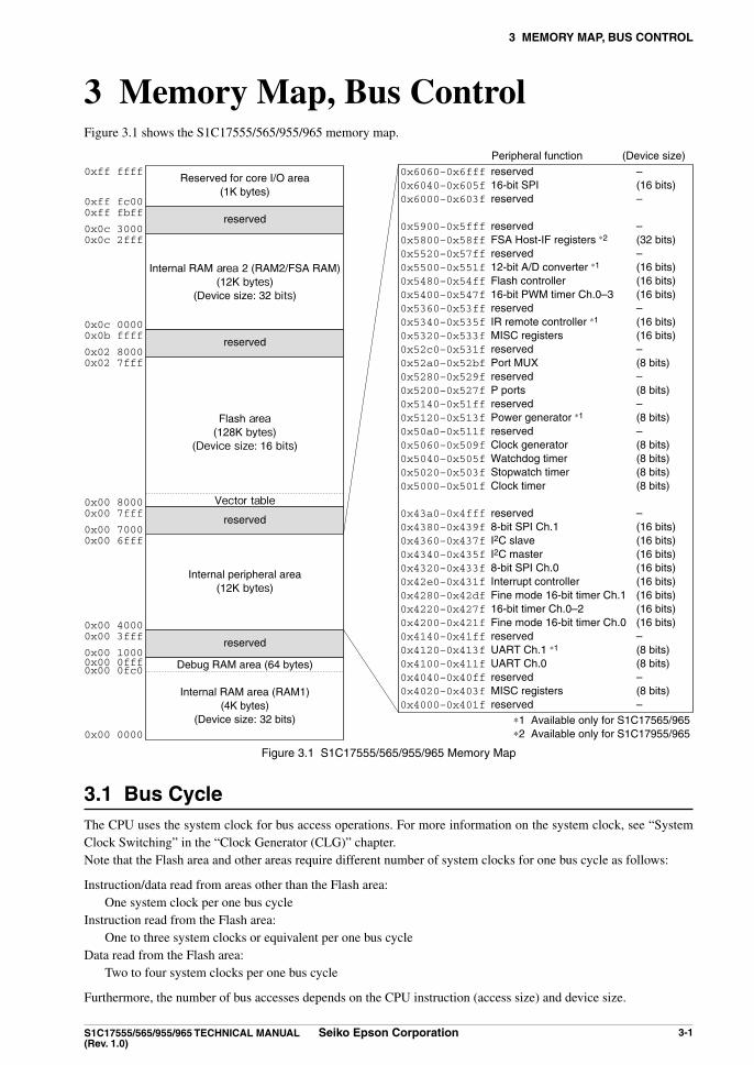
3 MeMORY MaP, BuS COnTROl
S1C17555/565/955/965 TeChniCal Manual Seiko epson Corporation 3-1(Rev. 1.0)
Memory Map, Bus Control3 Figure 3.1 shows the S1C17555/565/955/965 memory map.
Flash area(128K bytes)
(Device size: 16 bits)
Vector table
Internal peripheral area(12K bytes)
Reserved for core I/O area(1K bytes)
reserved
reserved
Internal RAM area 2 (RAM2/FSA RAM)(12K bytes)
(Device size: 32 bits)
reserved
0xff ffff
0xff fc000xff fbff
0x0c 30000x0c 2fff
0x0c 00000x0b ffff
0x02 80000x02 7fff
0x00 80000x00 7fff
0x00 70000x00 6fff
0x00 40000x00 3fff
0x00 10000x00 0fff0x00 0fc0
0x00 0000∗1 Available only for S1C17565/965∗2 Available only for S1C17955/965
reserved
Debug RAM area (64 bytes)
Internal RAM area (RAM1)(4K bytes)
(Device size: 32 bits)
0x6060–0x6fff0x6040–0x605f0x6000–0x603f
0x5900–0x5fff0x5800–0x58ff0x5520–0x57ff0x5500–0x551f0x5480–0x54ff0x5400–0x547f0x5360–0x53ff0x5340–0x535f0x5320–0x533f0x52c0–0x531f0x52a0–0x52bf0x5280–0x529f0x5200–0x527f0x5140–0x51ff0x5120–0x513f0x50a0–0x511f0x5060–0x509f0x5040–0x505f0x5020–0x503f0x5000–0x501f
0x43a0–0x4fff0x4380–0x439f0x4360–0x437f0x4340–0x435f0x4320–0x433f0x42e0–0x431f0x4280–0x42df0x4220–0x427f0x4200–0x421f0x4140–0x41ff0x4120–0x413f0x4100–0x411f0x4040–0x40ff0x4020–0x403f0x4000–0x401f
reserved16-bit SPIreserved
reservedFSA Host-IF registers ∗2
reserved12-bit A/D converter ∗1
Flash controller16-bit PWM timer Ch.0–3reservedIR remote controller ∗1
MISC registersreservedPort MUXreservedP portsreservedPower generator ∗1
reservedClock generatorWatchdog timerStopwatch timerClock timer
reserved8-bit SPI Ch.1I2C slaveI2C master8-bit SPI Ch.0Interrupt controllerFine mode 16-bit timer Ch.116-bit timer Ch.0–2Fine mode 16-bit timer Ch.0reservedUART Ch.1 ∗1
UART Ch.0reservedMISC registersreserved
–(16 bits)–
–(32 bits)–(16 bits)(16 bits)(16 bits)–(16 bits)(16 bits)–(8 bits)–(8 bits)–(8 bits)–(8 bits)(8 bits)(8 bits)(8 bits)
–(16 bits)(16 bits)(16 bits)(16 bits)(16 bits)(16 bits)(16 bits)(16 bits)–(8 bits)(8 bits)–(8 bits)–
Peripheral function (Device size)
1 S1C17555/565/955/965 Memory MapFigure 3.
Bus Cycle3.1 The CPU uses the system clock for bus access operations. For more information on the system clock, see “System Clock Switching” in the “Clock Generator (CLG)” chapter.Note that the Flash area and other areas require different number of system clocks for one bus cycle as follows:
Instruction/data read from areas other than the Flash area: One system clock per one bus cycleInstruction read from the Flash area: One to three system clocks or equivalent per one bus cycleData read from the Flash area: Two to four system clocks per one bus cycle
Furthermore, the number of bus accesses depends on the CPU instruction (access size) and device size.

3 MeMORY MaP, BuS COnTROl
3-2 Seiko epson Corporation S1C17555/565/955/965 TeChniCal Manual (Rev. 1.0)
1.1 Number of Bus AccessesTable 3.
Device size CPu access size number of bus accesses
8 bits 8 bits 116 bits 232 bits* 4
16 bits 8 bits 116 bits 132 bits* 2
32 bits 8 bits 116 bits 132 bits* 1
* Handling the eight high-order bits during 32-bit accesses The size of the S1C17 Core general-purpose registers is 24 bits. During writing, the eight high-order bits are written as 0. During reading from a memory, the eight high-order
bits are ignored. However, the stack operation in an interrupt handling reads/writes 32-bit data that consists of the PSR value as the high-order 8 bits and the return address as the low order 24 bits.
For more information, refer to the “S1C17 Core Manual.”
Restrictions on access Size3.1.1
The peripheral modules can be accessed with an 8-bit, 16-bit, or 32-bit instruction. However, reading for an unnec-essary register may change the peripheral module status and it may cause a problem. Therefore, use the appropriate instructions according to the device size.
Restrictions on instruction execution Cycles3.1.2
An instruction fetch and a data access are not performed simultaneously under one of the conditions listed below. This prolongs the instruction fetch cycle for the number of data area bus cycles.
• When the S1C17555/565/955/965 executes the instruction stored in the Flash area and accesses data in the Flash area
• When the S1C17555/565/955/965 executes the instruction stored in the internal RAM area and accesses data in the internal RAM area
Flash area3.2
embedded Flash Memory3.2.1
The 128K-byte area from address 0x8000 to address 0x27fff contains a Flash memory (2K bytes × 64 sectors) for storing application programs and data. Address 0x8000 is defined as the vector table base address, therefore a vec-tor table (see “Vector Table” in the “Interrupt Controller (ITC)” chapter) must be placed from the beginning of the area. The vector table base address can be modified with the MISC_TTBRL/MISC_TTBRH registers.
Flash Programming 3.2.2
The S1C17555/565/955/965 supports on-board programming of the Flash memory, it makes it possible to program the Flash memory with the application programs/data by using the debugger through an ICDmini. The Flash mem-ory supports sector erase method.For the Flash programming using the debugger, see the “S5U1C17001C Manual” included in the S1C17 Family C Compiler Package. For the self-programming controlled by the user program, please contact Seiko Epson.
Protect Bits3.2.3
In order to protect the memory contents, the Flash memory provides two protection features, write protection and data read protection, that can be configured for every 16K-byte areas. The write protection disables writing data to the configured area and erasing the sectors (except the sector that includes the protect bits).

3 MeMORY MaP, BuS COnTROl
S1C17555/565/955/965 TeChniCal Manual Seiko epson Corporation 3-3(Rev. 1.0)
The data-read protection disables reading data from the configured area (the read value is always 0x0000). How-ever, it does not disable the instruction fetch operation by the CPU.The Flash memory provides the protect bits listed below. Program the protect bit corresponding to the area to be protected to 0.The protection can only be disabled using the debugger.
Flash Protect Bitsaddress Bit Function Setting init. R/W Remarks
0x27ffc(16 bits)
D15–8 reserved – – –D7 reserved 1 1 R/W Always set to 1.D6 Flash write-protect bit for 0x20000–0x23fff 1 Writable 0 Protected 1 R/WD5 Flash write-protect bit for 0x1c000–0x1ffff 1 Writable 0 Protected 1 R/WD4 Flash write-protect bit for 0x18000–0x1bfff 1 Writable 0 Protected 1 R/WD3 Flash write-protect bit for 0x14000–0x17fff 1 Writable 0 Protected 1 R/WD2 Flash write-protect bit for 0x10000–0x13fff 1 Writable 0 Protected 1 R/WD1 Flash write-protect bit for 0xc000–0xffff 1 Writable 0 Protected 1 R/WD0 Flash write-protect bit for 0x8000–0xbfff 1 Writable 0 Protected 1 R/W
0x27ffe(16 bits)
D15–8 reserved – – –D7 Flash data-read-protect bit for 0x24000–0x27fff 1 Readable 0 Protected 1 R/WD6 Flash data-read-protect bit for 0x20000–0x23fff 1 Readable 0 Protected 1 R/WD5 Flash data-read-protect bit for 0x1c000–0x1ffff 1 Readable 0 Protected 1 R/WD4 Flash data-read-protect bit for 0x18000–0x1bfff 1 Readable 0 Protected 1 R/WD3 Flash data-read-protect bit for 0x14000–0x17fff 1 Readable 0 Protected 1 R/WD2 Flash data-read-protect bit for 0x10000–0x13fff 1 Readable 0 Protected 1 R/WD1 Flash data-read-protect bit for 0xc000–0xffff 1 Readable 0 Protected 1 R/WD0 reserved 1 1 R/W Always set to 1.
notes: • Be sure not to locate the area with data-read protection into the .data and .rodata sections.
• Be sure to set D0 of address 0x27ffe to 1. If it is set to 0, the program cannot be booted.
Flash Memory Read Wait Cycle Setting 3.2.4
In order to read data from the Flash memory properly, set the appropriate number of wait cycles according to the system clock frequency using the RDWAIT[1:0]/FLASHC_WAIT register.
FlaShC Read Wait Control Register (FlaShC_WaiT)Register name address Bit name Function Setting init. R/W Remarks
FlaShC Read Wait Control Register(FlaShC_WaiT)
0x54b0(16 bits)
D15–2 – reserved – – – 0 when being read.D1–0 RDWaiT
[1:0]Flash read wait cycle RDWAIT[1:0] Wait 0x3 R/W
0x30x20x10x0
2 wait1 wait
No waitreserved
D[1:0] RDWaiT[1:0]: Flash Read Wait Cycle Bits Sets the number of wait cycles for reading from the Flash memory. One wait insertion prolongs bus
cycles by one system clock cycle. For the configurable wait cycles, see the “Electrical Characteristics” chapter.
Bus cycle when “no wait” is selected Instruction read: 1 bus cycle = 1 system clock cycle or equivalent Data read: 1 bus cycle = 2 system clock cycles
note: Be sure to avoid setting a number of wait cycles that exceeds the maximum allowable system clock frequency, as it may cause a malfunction.

3 MeMORY MaP, BuS COnTROl
3-4 Seiko epson Corporation S1C17555/565/955/965 TeChniCal Manual (Rev. 1.0)
internal RaM area3.3
embedded RaM3.3.1
The S1C17555/565/955/965 contains RAM1 in the 4K-byte area from address 0x0 to address 0xfff and RAM2 in the 12K-byte area from address 0xc0000 to address 0xc2fff. The RAM allows high-speed execution of the instruc-tion codes copied into it as well as storing variables and other data.
notes: • The RAM2 of the S1C17955/965 is reserved for the FSA. It can not be used as a general-purpose RAM when the FSA is used.
• The 64-byte area at the end of the RAM1 (0xfc0–0xfff) is reserved for the on-chip debugger. When using the debug functions under application development, do not access this area from the application program.
This area can be used for applications of mass-produced devices that do not need debugging.
The S1C17555/565/955/965 enables the RAM1 size used to apply restrictions to 4KB, 2KB, 1KB, or 512B. For ex-ample, when using the S1C17555/565/955/965 to develop an application for a built-in ROM model, you can set the RAM1 size to match the embedded RAM of the target model, preventing creating programs that seek to access ar-eas outside the RAM areas of the target product. The RAM1 size is selected using IRAMSZ[2:0]/MISC_IRAMSZ register.
iRaM Size Register (MiSC_iRaMSZ)Register name address Bit name Function Setting init. R/W Remarks
iRaM Size Register(MiSC_iRaMSZ)
0x5326(16 bits)
D15–9 – reserved – – – 0 when being read.D8 DBaDR Debug base address select 1 0x0 0 0xfffc00 0 R/WD7 – reserved – – – 0 when being read.
D6–4 iRaMaCTSZ[2:0]
IRAM actual size 0x2 (= 4KB) 0x2 R
D3 – reserved – – – 0 when being read.D2–0 iRaMSZ[2:0] IRAM size select IRAMSZ[2:0] Size 0x2 R/W
0x7–0x60x50x40x30x2
0x1–0x0
reserved512B1KB2KB4KB
reserved
D[6:4] iRaMaCTSZ[2:0]: iRaM actual Size Bits Indicates the actual internal RAM size embedded. (Default: 0x2)
D[2:0] iRaMSZ[2:0]: iRaM Size Select Bits Selects the internal RAM size used.
3.1.1 Selecting Internal RAM SizeTable 3.
iRaMSZ[2:0] internal RaM size
0x7–0x6 Reserved0x5 512B0x4 1KB0x3 2KB0x2 4KB
0x1–0x0 Reserved
(Default: 0x2)
note: The MISC_IRAMSZ register is write-protected. The write-protection must be overridden by writing 0x96 to the MISC_PROT register. Note that the MISC_PROT register should normally be set to a value other than 0x96, except when writing to the MISC_IRAMSZ register. Unnecessary programs may result in system malfunctions.

3 MeMORY MaP, BuS COnTROl
S1C17555/565/955/965 TeChniCal Manual Seiko epson Corporation 3-5(Rev. 1.0)
internal Peripheral area3.4 The I/O and control registers for the internal peripheral modules shown below are located in the 12K-byte area be-ginning with address 0x4000.For details of each control register, see the I/O register list in Appendix or description for each peripheral module.
• MISC register (MISC, 8-bit device)• UART (UART, 8-bit device)• Fine mode 16-bit timers (T16F, 16-bit device)• 16-bit timers (T16, 16-bit device)• Interrupt controller (ITC, 16-bit device)• 8-bit SPI (SPI, 16-bit device)• I2C master (I2CM, 16-bit device)• I2C slave (I2CS, 16-bit device)• Clock timer (CT, 8-bit device)• Stopwatch timer (SWT, 8-bit device)• Watchdog timer (WDT, 8-bit device)• Clock generator (CLG, 8-bit device)• Power generator (VD1, 8-bit device) Available only for S1C17565/965• I/O port & port MUX (P, 8-bit device)• MISC register (MISC, 16-bit device)• IR remote controller (REMC, 16-bit device) Available only for S1C17565/965• 16-bit PWM timers (T16A2, 16-bit device)• Flash controller (FLASHC, 16-bit device)• 12-bit A/D converter (ADC12SA2, 16-bit device) Available only for S1C17565/965• FSA Host-IF registers (FSA, 32-bit device) Available only for S1C17955/965• 16-bit SPI (SPI16, 16-bit device)
S1C17 Core i/O area3.5 The 1K-byte area from address 0xfffc00 to address 0xffffff is the I/O area for the CPU core in which the I/O regis-ters listed in the table below are located.
5.1 I/O Map (S1C17 Core I/O Area)Table 3.
Peripheral address Register name FunctionS1C17 Core I/O 0xffff84 IDIR Processor ID Register Indicates the processor ID.
0xffff90 DBRAM Debug RAM Base Register Indicates the debug RAM base address.0xffffa0 DCR Debug Control Register Debug control0xffffb4 IBAR1 Instruction Break Address Register 1 Instruction break address #1 setting0xffffb8 IBAR2 Instruction Break Address Register 2 Instruction break address #2 setting0xffffbc IBAR3 Instruction Break Address Register 3 Instruction break address #3 setting0xffffd0 IBAR4 Instruction Break Address Register 4 Instruction break address #4 setting
See “Processor Information” in the “CPU” chapter for more information on IDIR. See the “On-chip Debugger (DBG)” chapter for more information on other registers.This area includes the S1C17 Core registers, in addition to those described above. For more information on these registers, refer to the “S1C17 Core Manual.”

4 POWeR SuPPlY
S1C17555/565/955/965 TeChniCal Manual Seiko epson Corporation 4-1(Rev. 1.0)
Power Supply4
Core Power Supply Voltage (lV4.1 DD)The CPU core and internal logic circuits operate with a voltage supplied between the LVDD and VSS pins. Supply a voltage within the range shown below to the LVDD pins with the VSS pins as the GND level.
LVDD = 1.65 V to 1.95 V (VSS = GND)
The S1C17555/565/955/965 provides two or more LVDD and VSS pins. Do not leave any power supply pins open and be sure to connect them to + power source and GND.The S1C17565/965 is able to operate with a 2.0 V to 3.6 V (3.1 V to 3.6 V when the analog circuit or Flash pro-gramming power supply is used) single power supply. In this case, the core power voltage can be generated using the embedded 1.8 V regulator and supplied as the LVDD voltage.
i/O Power Supply Voltage (hV4.2 DD)The HVDD voltage is used for interfacing with external I/O signals. Supply a voltage within the range shown below to the HVDD pins with the VSS pins as the GND level.
HVDD = 1.65 V to 3.6 V (VSS = GND)
The S1C17555/565/955/965 provides two or more HVDD pins. Do not leave any power supply pins open and be sure to connect them to the power source.
note: When an external clock is input to the OSC3 or OSC1 pin, the clock signal level must be LVDD.
analog Power Supply Voltage (aV4.3 DD) [S1C17565/965]AVDD is the power supply voltage for the S1C17565/965 internal analog circuits. Connecting a power supply iso-lated from HVDD to the AVDD pin eliminates effects due to noise generated by digital circuits, allowing the analog circuit to measure with high accuracy. Supply a voltage within the range shown below to the AVDD pins with the AVSS pins as the GND level.
AVDD = 2.7 V to 3.6 V (AVSS = GND)
note: When the analog circuit (12-bit A/D converter) is not used, supply a voltage same as the HVDD level to the AVDD and VINA pins.
The S1C17565/965 can also generate the AVDD voltage with an internal regulator (VINA = 3.1 V to 3.6 V). To perform measurement with high accuracy, design the AVDD trace on the printed circuit board so that noise will not affect the AVDD power line.
Flash Programming Power Supply Voltage (V4.4 PP)The VPP voltage is used for erasing/programming the embedded Flash memory. Supply a voltage shown below to the VPP pin with the VSS pins as the GND level to program the Flash memory.
VPP = 7.5 V (VSS = GND)
note: Leave the VPP pin open during normal operation.
The S1C17565/965 can also generate the VPP voltage with an internal regulator (2.4 V to 3.6 V input) and a voltage booster circuit.
4 POWeR SuPPlY
4-2 Seiko epson Corporation S1C17555/565/955/965 TeChniCal Manual (Rev. 1.0)
embedded Regulators4.5
lV4.5.1 DD Regulator [S1C17565/965]
The S1C17565/965 includes an LVDD regulator that allows use of a single power supply for IC operations.
Regulator input (VINL): 2.0 V to 3.6 VRegulator output (LVDD): 1.8 V
When the LVDD regulator is used, supply a voltage within the range shown above to the VINL pin. Also the same voltage should be supplied to the REGEN pin to enable the regulator to operate. The LVDD regulator generates an LVDD voltage and supplies it to the core and internal circuits.For power supply connection examples, see the “Basic External Connection Diagram” chapter.
The LVDD regulator supports economy mode (power saving mode) to reduce current consumption in the regulator during low-speed (32 kHz) operation or standby mode (HALT or SLEEP).
aV4.5.2 DD Regulator [S1C17565/965]
The S1C17565/965 includes an AVDD regulator to generate the operating voltage for the internal analog circuits.
Regulator input (VINA): 3.1 V to 3.6 VRegulator output (AVDD): 2.8 V
The internal power supply for the analog circuits and the AVDD pin status can be controlled using the ADC12_ACTL register as follows:
5.2.1 Internal Power Supply Register Settings for Analog CircuitsTable 4.
Control conditionaDC12_aCTl register settings
RG_Be (D3) RG_Ce (D2)
AVDD supplied externally 0 0AVDD generated internally 1 112-bit A/D converter not used * 0 0
* When the analog circuits are not used, set the AVDD and VINA pins to the same voltage level as HVDD.
For power supply connection examples, see the “Basic External Connection Diagram” chapter.
note: The AVDD regulator output cannot be supplied to external devices through the AVDD pin.
V4.5.3 PP Regulator/Booster
The S1C17555/565/955/965 includes a VPP regulator/booster circuit for internally generating the VPP voltage to erase/program the Flash memory.
Regulator input (VINP): 2.4 V to 3.6 VRegulator output (VPP): 7.5 V
When the VPP regulator/booster circuit is used, supply a voltage within the range shown above to the VINP pin.The voltage booster requires external capacitors. Connect a capacitor with appropriate capacitance between the C1P and C1N pins, between the C1H pin and VSS, between the C2P and C2N pins, and the VPP pin and VSS. For connec-tion diagram and recommended capacitance values, see the “Basic External Connection Diagram” chapter.The VPP regulator/booster circuit can be controlled via the Flash programming function in the debugger or the self-programming module. For the Flash programming using the debugger, see the “S5U1C17001C Manual” included in the S1C17 Family C Compiler Package. For the self-programming controlled by the user program, please contact Seiko Epson.

4 POWeR SuPPlY
S1C17555/565/955/965 TeChniCal Manual Seiko epson Corporation 4-3(Rev. 1.0)
Control Register Details [S1C17565/965]4.6
6.1 Power Control RegistersTable 4.
address Register name Function0x5121 VD1_CTL VD1 Control Register Controls the regulator operation mode.0x550a ADC12_ACTL ADC12SA2 Power Control Register Controls ADC12SA2 power supply.
The power control registers are described in detail below.
note: When data is written to the registers, the “Reserved” bits must always be written as 0 and not 1.
VD1 Control Register (VD1_CTl)Register name address Bit name Function Setting init. R/W Remarks
VD1 Control Register(VD1_CTl)
S1C17565/965
0x5121(8 bits)
D7–2 – reserved – – – 0 when being read.D1–0 VD1eCO
[1:0]Regulator operation mode select VD1ECO[1:0] Mode 0x0 R/W
0x30x20x10x0
reservedAuto-control
EconomyNormal
D[7:2] Reserved
D[1:0] VD1eCO[1:0]: Regulator Operation Mode Select Bits [S1C17565/965] Sets the operation mode of the embedded regulator.
6.2 Regulator Operation ModeTable 4.
VD1eCO[1:0] Operation mode
0x3 Reserved0x2 Auto-control mode0x1 Economy (power saving) mode0x0 Normal mode
(Default: 0x0)
For normal operation (while the IC is operating with a clock other than OSC1), set VD1ECO[1:0] to 0x0 (default).
Setting VD1ECO[1:0] to 0x1 places the regulator into economy mode. The economy mode can reduce current consumption, note, however, that the regulator may become unstable due to changes of load that cannot be responded. The regulator should be set to economy mode before the slp instruction is execut-ed.
Setting VD1ECO[1:0] to 0x2 places the regulator into auto-control mode. In this mode, the hardware automatically performs switching between normal mode and economy mode according to changes of load. The regulator enters economy mode when both IOSC and OSC3 are stopped or when the IC en-ters SLEEP mode, or enters normal mode otherwise.
While the IC is operating with a high-speed clock (other than OSC1), the regulator should not be set to economy mode, as the regulator output voltage may become unstable. Even if the IC is operating with OSC1, set the regulator to normal mode when driving a heavy load such as a lamp or buzzer.
aDC12Sa2 Power Control Register (aDC12_aCTl)Register name address Bit name Function Setting init. R/W Remarks
aDC12Sa2 Power Control Register(aDC12_aCTl)
S1C17565/965
0x550a(16 bits)
D15–4 – reserved – – – 0 when being read.
D3 RG_Be Reference voltage source enable 1 Enable 0 Disable 0 R/WD2 RG_Ce AVDD enable 1 Enable 0 Disable 0 R/W
D1–0 – reserved – – – 0 when being read.
note: Make sure that CTLEN/ADC12_CTL0 register is set to 0 and MSBUSY/ADC12_CTL1 is set to 0 before altering this register.
D[15:4] Reserved

4 POWeR SuPPlY
4-4 Seiko epson Corporation S1C17555/565/955/965 TeChniCal Manual (Rev. 1.0)
D3 RG_Be: Reference Voltage Source enable Bit [S1C17565/965] Enables or disables the internal reference voltage source. 1 (R/W): Enabled (on) 0 (R/W): Disabled (off) (default)
When RG_BE is set to 1, the internal reference voltage source goes on. Setting RG_BE to 0 turns the internal reference voltage source off. Set RG_BE to 1 when the AVDD regulator is used.
D2 RG_Ce: aVDD enable Bit [S1C17565/965] Enables or disables the AVDD pin output. 1 (R/W): Enabled 0 (R/W): Disabled (default)
When RG_CE is set to 1, the AVDD regulator is activated and the voltage generated by the AVDD regula-tor is output from the AVDD pin. Fix RG_CE at 0 if an external AVDD voltage is supplied.
D[1:0] Reserved
Precautions on Power Supply4.7
Power-on sequence In order to operate the device normally, supply power in accordance with the following timing.
HVDD, AVDD
LVDD
IOSC
#RESET
LVDD min.
tLVDD
tSTA tRST
7.1 Power-On SequenceFigure 4.
(1) tLVDD: Elapsed time until the power supply stabilizes after power-on Supply power in the following sequence: Power-on: LVDD → HVDD (I/O), AVDD (A/D) → Apply the input signal or LVDD, HVDD (I/O), AVDD (A/D) → Apply the input signal (See Notes in “Power-off sequence” below.)
(2) tSTA: Time at which IOSC oscillation starts
(3) tRST: Minimum reset pulse width Time at which the clock supplied to the chip stabilizes plus at least six clocks; Keep the #RESET sig-
nal low.
note: When the HVDD power is turned on from off status, stable internal circuit statuses cannot be guar-anteed due to noise in the power line. Therefore, the circuit statuses must be initialized (reset) after the power is turned on.
Power-off sequence Shut off the power supply in the following sequence: Power-off: Turn off the input signal → HVDD (I/O), AVDD (A/D) → LVDD
or Turn off the input signal → HVDD (I/O), AVDD (A/D), LVDD (See Notes below.)
notes: • Applying only LVDD with other power voltage turned off puts the HVDD system circuits into un-stable status and unstable current flows in the I/O cells. Be sure to avoid applying only LVDD for a duration of one second or more.
• Be sure to avoid applying HVDD or AVDD for a duration of one second or more when the LVDD power is off, as a breakdown may occur in the device or the characteristics may be degraded due to flow-through current of the HVDD or AVDD.
4 POWeR SuPPlY
S1C17555/565/955/965 TeChniCal Manual Seiko epson Corporation 4-5(Rev. 1.0)
latch-up The CMOS device may be in the latch-up condition. This is the phenomenon caused by conduction of the para-
sitic PNPN junction (thyristor) contained in the CMOS IC, resulting in a large current between HVDD and VSS and leading to breakage.
Latch-up occurs when the voltage applied to the input / output exceeds the rated value and a large current flows into the internal element, or when the voltage at the HVDD pin exceeds the rated value and the internal element is in the breakdown condition. In the latter case, even if the application of a voltage exceeding the rated value is instantaneous, the current remains high between HVDD and VSS once the device is in the latch-up condition. As this may result in heat generation or smoking, the following points must be taken into consideration:(1) The voltage level at the input/output must not exceed the range specified in the electrical characteristics. In
other words, it must be below the power-supply voltage and above VSS. The power-on timing should also be taken into consideration.
(2) Abnormal noise must not be applied to the device.(3) The potential at the unused input should be fixed at HVDD, AVDD, or VSS.(4) No outputs should be shorted.

5 iniTial ReSeT
S1C17555/565/955/965 TeChniCal Manual Seiko epson Corporation 5-1(Rev. 1.0)
Initial Reset5
initial Reset Sources5.1 The S1C17555/565/955/965 has three initial reset sources that initialize the internal circuits.
(1) #RESET pin (external initial reset)(2) Key-entry reset using the P0 ports (P00–P03 pins) (software selectable external initial reset)(3) Watchdog timer (software selectable internal initial reset)
Figure 5.1.1 shows the configuration of the initial reset circuit.
P0 ports
#RESET
Key-entry reset signal
Reset input signal
Internal reset signal(to core and peripheral modules)
WDT reset signal
P00P01P02P03
Watchdog timer
1.1 Configuration of Initial Reset CircuitFigure 5.
The CPU and peripheral circuits are initialized by the active signal from an initial reset source. When the reset sig-nal is negated, the CPU starts reset handling. The reset handling reads the reset vector (reset handler start address) from the beginning of the vector table and starts executing the program (initial routine) beginning with the read ad-dress.
#ReSeT Pin5.1.1
By setting the #RESET pin to low level, the S1C17555/565/955/965 enters initial reset state. In order to initialize the S1C17555/565/955/965 for sure, the #RESET pin must be held at low for more than the prescribed time (see “AC Characteristics” in the “Electrical Characteristics” chapter) after the power supply voltage is supplied.Initial reset state is canceled when the #RESET pin at low level is set to high level and the CPU starts executing the reset interrupt handler.The #RESET pin is equipped with a pull-up resistor.
P0 Port Key-entry Reset 5.1.2
Entering low level simultaneously to the ports (P00–P03) selected with software triggers an initial reset. For details of the key-entry reset function, see the “I/O Ports (P)” chapter.
note: The P0 port key-entry reset function cannot be used for power-on reset as it must be enabled with software.
Resetting by the Watchdog Timer5.1.3
The S1C17555/565/955/965 has a built-in watchdog timer to detect runaway of the CPU. The watchdog timer over-flows if it is not reset with software (due to CPU runaway) in the WDT reset cycles according to the clock selected using a WDT register. The overflow signal can generate either NMI or reset. Write 1 to the WDTMD/WDT_ST register to generate reset (NMI occurs when WDTMD = 0).For details of the watchdog timer, see the “Watchdog Timer (WDT)” chapter.

5 iniTial ReSeT
5-2 Seiko epson Corporation S1C17555/565/955/965 TeChniCal Manual (Rev. 1.0)
notes: • When using the reset function of the watchdog timer, program the watchdog timer so that it will be reset within the set cycles to avoid occurrence of an unnecessary reset.
• The reset function of the watchdog timer cannot be used for power-on reset as it must be en-abled with software.
initial Reset Sequence5.2 Even if the #RESET pin input negates the reset signal after power is turned on, the CPU cannot boot up until the IOSC oscillation stabilization waiting time (64 cycles), system clock internal supply start time (8 cycles), and Flash reset cancellation time (32 cycles) have elapsed. Figure 5.2.1 shows the operating sequence following cancellation of initial reset.The CPU starts operating in synchronization with the IOSC clock after reset state is canceled.
note: The oscillation stabilization time described in this section does not include oscillation start time. Therefore the time interval until the CPU starts executing instructions after power is turned on or SLEEP mode is canceled may be longer than that indicated in the figure below.
Boot vector
Oscillation stabilization waiting time(64 cycles)
System clock internal supply start time
(8 cycles)
Flash reset canceling time
(32 cycles)
Booting
IOSC clock
System clock
#RESET
Internal reset
Internal data request
Internal data address
Internal reset canceled
Reset canceled
2.1 Operation Sequence Following Cancellation of Initial ResetFigure 5.
initial Settings after an initial Reset 5.3 The CPU internal registers are initialized as follows at initial reset.R0–R7: 0x0PSR: 0x0 (interrupt level = 0, interrupt disabled) SP: 0x0PC: Reset vector stored at the beginning of the vector table is loaded by the reset handling.
The internal RAM should be initialized with software as it is not initialized at initial reset.The internal peripheral modules are initialized to the default values (except some undefined registers). Change the settings with software if necessary. For the default values set at initial reset, see the list of I/O registers in Appendix or descriptions for each peripheral module.

6 inTeRRuPT COnTROlleR (iTC)
S1C17555/565/955/965 TeChniCal Manual Seiko epson Corporation 6-1(Rev. 1.0)
Interrupt Controller (ITC)6
iTC Module Overview6.1 The interrupt controller (ITC) honors interrupt requests from the peripheral modules and outputs the interrupt re-quest, interrupt level and vector number signals to the S1C17 Core according to the priority and interrupt levels.The features of the ITC module are listed below.
• S1C17555: Supports 18 maskable interrupt systems (19 interrupt sources). S1C17565: Supports 20 maskable interrupt systems (22 interrupt sources). S1C17955: Supports 20 maskable interrupt systems (21 interrupt sources). S1C17965: Supports 22 maskable interrupt systems (24 interrupt sources).
interrupt system
interrupt S1C17555 S1C17565 S1C17955 S1C17965
1 P0 port interrupt (8 types)2 P1 port interrupt (8 types)3 Stopwatch timer interrupt (3 types)4 Clock timer interrupt (4 types)5 16-bit PWM timer Ch.2 interrupt (4 types)6 16-bit SPI interrupt (4 types)7 16-bit PWM timer Ch.0 interrupt (4 types)8 Fine mode 16-bit timer Ch.0/Ch.1 interrupt (2 types)9 16-bit timer Ch.0 interrupt (1 type)10 16-bit timer Ch.1 interrupt (1 type)11 16-bit timer Ch.2 interrupt (1 type)
16-bit PWM timer Ch.3 interrupt (4 types)12 UART Ch.0 interrupt (4 types) 13 UART Ch.1 interrupt (4 types) – –14 8-bit SPI Ch.0 interrupt (2 types) 15 I2C master interrupt (2 types) 16 IR remote controller interrupt (3 types) – –
8-bit SPI Ch.1 interrupt (2 types) 17 16-bit PWM timer Ch.1 interrupt (4 types)18 12-bit A/D converter interrupt (5 types) – –19 FSA (IRQ1) interrupt (1 type) – –20 P2 port interrupt (4 types or 8 types)21 I2C slave interrupt (3 types)22 FSA (IRQ0) interrupt (1 type) – –
• Supports eight interrupt levels to prioritize the interrupt sources.
The ITC enables the interrupt level (priority) for determining the processing sequence when multiple interrupts oc-cur simultaneously to be set for each interrupt system separately.Each interrupt system includes the number of interrupt causes indicated in parentheses above. Settings to enable or disable interrupt for different causes are set by the respective peripheral module registers.For specific information on interrupt causes and their control, refer to the peripheral module explanations.Figure 6.1.1 shows the structure of the interrupt system.

6 inTeRRuPT COnTROlleR (iTC)
6-2 Seiko epson Corporation S1C17555/565/955/965 TeChniCal Manual (Rev. 1.0)
S1C17 Core interrupt controller
Watchdog timer
Interrupt request
Interruptlevel
Vectornumber
Debug signalReset signal
Interrupt request
NMI
Interrupt level
Interruptcontrol
Vector number
Interrupt level
Vector number
Interrupt request
• •
• •
•
• •
•
Peripheral module
Interrupt enable
Cause of interrupt 1
Interrupt enable
Cause of interrupt n
• •
• •
Interrupt flag
Interrupt flag
Peripheral module
Interrupt enable
Cause of interrupt 1
Interrupt enable
Cause of interrupt n
• •
• •
Interrupt flag
Interrupt flag
1.1 Interrupt SystemFigure 6.
Vector Table6.2 The vector table contains the vectors to the interrupt handler routines (handler routine start address) that will be read by the S1C17 Core to execute the handler when an interrupt occurs. Table 6.2.1 shows the vector table of the S1C17555/565/955/965.
2.1 Vector TableTable 6.
Vector no.Software interrupt no.
Vector address hardware interrupt name Cause of interrupt Priority
0 (0x00) TTBR + 0x00 Reset • Low input to the #RESET pin• Watchdog timer overflow *2
1
1 (0x01) TTBR + 0x04 Address misaligned interrupt Memory access instruction 2– (0xfffc00) Debugging interrupt brk instruction, etc. 3
2 (0x02) TTBR + 0x08 NMI Watchdog timer overflow *2 43 (0x03) TTBR + 0x0c Reserved for C compiler – –4 (0x04) TTBR + 0x10 P0 port interrupt P00–P07 port inputs High *1
5 (0x05) TTBR + 0x14 P1 port interrupt P10–P17 port inputs ↑6 (0x06) TTBR + 0x18 Stopwatch timer interrupt • 100 Hz timer signal
• 10 Hz timer signal• 1 Hz timer signal
7 (0x07) TTBR + 0x1c Clock timer interrupt • 32 Hz timer signal• 8 Hz timer signal• 2 Hz timer signal• 1 Hz timer signal
8 (0x08) TTBR + 0x20 16-bit PWM timer Ch.2 interrupt • Compare A/B• Capture A• Capture A overwrite
9 (0x09) TTBR + 0x24 reserved –10 (0x0a) TTBR + 0x28 16-bit SPI interrupt • Transmit buffer empty
• Receive buffer overwrite error• Receive buffer full• Software control
11 (0x0b) TTBR + 0x2c 16-bit PWM timer Ch.0 interrupt • Compare A/B• Capture A• Capture A overwrite
12 (0x0c) TTBR + 0x30 Fine mode 16-bit timer Ch.0 and Ch.1 interrupt
• Ch.0 underflow• Ch.1 underflow
13 (0x0d) TTBR + 0x34 16-bit timer Ch.0 interrupt Timer underflow14 (0x0e) TTBR + 0x38 16-bit timer Ch.1 interrupt Timer underflow

6 inTeRRuPT COnTROlleR (iTC)
S1C17555/565/955/965 TeChniCal Manual Seiko epson Corporation 6-3(Rev. 1.0)
Vector no.Software interrupt no.
Vector address hardware interrupt name Cause of interrupt Priority
15 (0x0f) TTBR + 0x3c 16-bit timer Ch.2 interrupt Timer underflow16-bit PWM timer Ch.3 interrupt • Compare A/B
• Capture A• Capture A overwrite
16 (0x10) TTBR + 0x40 UART Ch.0 interrupt • Transmit buffer empty• End of transmission• Receive buffer full• Receive error
17 (0x11) TTBR + 0x44 UART Ch.1 interrupt[S1C17565/965]
• Transmit buffer empty• End of transmission• Receive buffer full• Receive error
18 (0x12) TTBR + 0x48 8-bit SPI Ch.0 interrupt • Transmit buffer empty• Receive buffer full
19 (0x13) TTBR + 0x4c I2C Master interrupt • Transmit buffer empty• Receive buffer full
20 (0x14) TTBR + 0x50 IR remote controller interrupt[S1C17565/965]
• Data length counter underflow• Input rising edge detected• Input falling edge detected
8-bit SPI Ch.1 interrupt • Transmit buffer empty• Receive buffer full
21 (0x15) TTBR + 0x54 16-bit PWM timer Ch.1 interrupt • Compare A/B• Capture A• Capture A overwrite
22 (0x16) TTBR + 0x58 12-bit A/D converter interrupt[S1C17565/965]
Measurement completion All/Ch.8/Ch.7/Ch.6/Ch.3~5
23 (0x17) TTBR + 0x5c FSA interrupt [S1C17955/965] IRQ124 (0x18) TTBR + 0x60 P2 port interrupt P20–P23/27 port inputs25 (0x19) TTBR + 0x64 reserved –26 (0x1a) TTBR + 0x68 I2C Slave interrupt • Transmit buffer empty
• Receive buffer full• Bus status
27 (0x1b) TTBR + 0x6c FSA interrupt [S1C17955/965] IRQ028 (0x1c) TTBR + 0x70 reserved –
: : : : ↓31 (0x1f) TTBR + 0x7c reserved – Low *1
*1 When the same interrupt level is set*2 Either reset or NMI can be selected as the watchdog timer interrupt with software.
Vector numbers 4 to 27 are assigned to the maskable interrupts supported by the S1C17555/565/955/965.
interrupts that share an interrupt vector Interrupt vector numbers 15 and 20 are shared with two different interrupt modules. Interrupt vector 15: 16-bit timer Ch.2 and 16-bit PWM timer Ch.3 Interrupt vector 20: IR remote controller and 16-bit SPI
The interrupt signals from the two modules are input to the ITC through an OR gate. When using the two inter-rupts, check if which interrupt has occurred by reading the interrupt flags in both modules.
The two modules cannot be set to different interrupt level, as they use the same interrupt vector.
Vector table base address The S1C17555/565/955/965 allows the base (starting) address of the vector table to be set using the MISC_
TTBRL and MISC_TTBRH registers. “TTBR” described in Table 6.2.1 means the value set to these registers. After an initial reset, the MISC_TTBRL and MISC_TTBRH registers are set to 0x8000. Therefore, even when the vector table location is changed, it is necessary that at least the reset vector be written to the above address. Bits 7 to 0 in the MISC_TTBRL register are fixed at 0, so the vector table starting address always begins with a 256-byte boundary address.

6 inTeRRuPT COnTROlleR (iTC)
6-4 Seiko epson Corporation S1C17555/565/955/965 TeChniCal Manual (Rev. 1.0)
Vector Table address low/high Registers (MiSC_TTBRl, MiSC_TTBRh)Register name address Bit name Function Setting init. R/W Remarks
Vector Table address low Register(MiSC_TTBRl)
0x5328(16 bits)
D15–8 TTBR[15:8] Vector table base address A[15:8] 0x0–0xff 0x80 R/WD7–0 TTBR[7:0] Vector table base address A[7:0]
(fixed at 0)0x0 0x0 R
Vector Table address high Register (MiSC_TTBRh)
0x532a(16 bits)
D15–8 – reserved – – – 0 when being read.D7–0 TTBR[23:16] Vector table base address
A[23:16]0x0–0xff 0x0 R/W
note: The MISC_TTBRL and MISC_TTBRH registers are write-protected. Before these registers can be rewritten, write protection must be removed by writing data 0x96 to the MISC_PROT register. Note that since unnecessary rewrites to the MISC_TTBRL and MISC_TTBRH registers could lead to erratic system operation, the MISC_PROT register should be set to other than 0x96 unless the Vector Table Base Registers must be rewritten.
Control of Maskable interrupts6.3
interrupt Control Bits in Peripheral Modules6.3.1 The peripheral module that generates interrupts includes an interrupt enable bit and an interrupt flag for each inter-rupt cause. The interrupt flag is set to 1 when the cause of interrupt occurs. By setting the interrupt enable bit to 1 (interrupt enabled), the flag state will be sent to the ITC as an interrupt request signal, generating an interrupt re-quest to the S1C17 Core. The corresponding interrupt enable bits should be set to 0 for those causes for which interrupts are not desired. In this case, although the interrupt flag is set to 1 if the interrupt cause occurs, the interrupt request signal sent to the ITC will not be asserted.For specific information on causes of interrupts, interrupt flags, and interrupt enable bits, refer to the respective pe-ripheral module descriptions.
note: To prevent recurrence of the interrupt due to the same cause of interrupt, always reset the inter-rupt flag in the peripheral module before enabling the interrupt, resetting the PSR, or executing the reti instruction.
iTC interrupt Request Processing6.3.2
On receiving an interrupt signal from a peripheral module, the ITC sends the interrupt request, interrupt level, and vector number signals to the S1C17 Core.Vector numbers are determined by the ITC internal hardware for each interrupt cause, as shown in Table 6.2.1.The interrupt level is a value used by the S1C17 Core to compare with the IL bits (PSR). This interrupt level is used in the S1C17 Core to disable subsequently occurring interrupts with the same or lower level. (See Section 6.3.3.)The default ITC settings are level 0 for all maskable interrupts. Interrupt requests are not accepted by the S1C17 Core if the level is 0.The ITC includes control bits for selecting the interrupt level, and the level can be set to between 0 (low) and 7 (high) interrupt levels for each interrupt type.If interrupt requests are input to the ITC simultaneously from two or more peripheral modules, the ITC outputs the interrupt request with the highest priority to the S1C17 Core in accordance with the following conditions.1. The interrupt with the highest interrupt level takes precedence.2. If multiple interrupt requests are input with the same interrupt level, the interrupt with the lowest vector number
takes precedence.
The other interrupts occurring at the same time are held until all interrupts with higher priority levels have been ac-cepted by the S1C17 Core.If an interrupt cause with higher priority occurs while the ITC is outputting an interrupt request signal to the S1C17Core (before being accepted by the S1C17 Core), the ITC alters the vector number and interrupt level signals to the setting information on the more recent interrupt. The previously occurring interrupt is held. The held interrupt is canceled and no interrupt is generated if the interrupt flag in the peripheral module is reset with software.
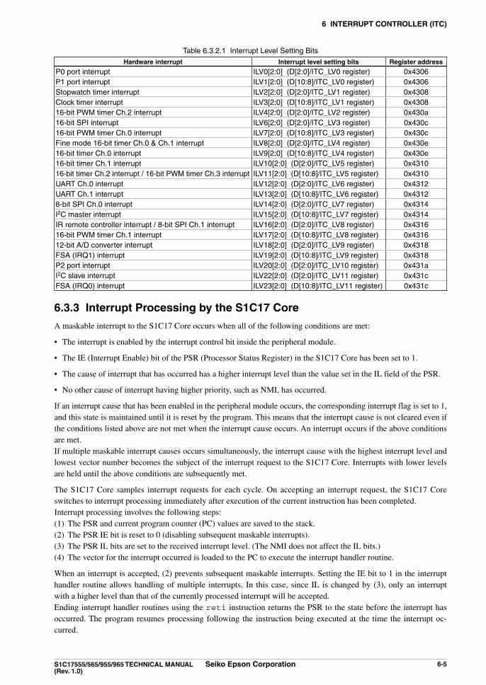
6 inTeRRuPT COnTROlleR (iTC)
S1C17555/565/955/965 TeChniCal Manual Seiko epson Corporation 6-5(Rev. 1.0)
3.2.1 Interrupt Level Setting BitsTable 6.
hardware interrupt interrupt level setting bits Register address
P0 port interrupt ILV0[2:0] (D[2:0]/ITC_LV0 register) 0x4306P1 port interrupt ILV1[2:0] (D[10:8]/ITC_LV0 register) 0x4306Stopwatch timer interrupt ILV2[2:0] (D[2:0]/ITC_LV1 register) 0x4308Clock timer interrupt ILV3[2:0] (D[10:8]/ITC_LV1 register) 0x430816-bit PWM timer Ch.2 interrupt ILV4[2:0] (D[2:0]/ITC_LV2 register) 0x430a16-bit SPI interrupt ILV6[2:0] (D[2:0]/ITC_LV3 register) 0x430c16-bit PWM timer Ch.0 interrupt ILV7[2:0] (D[10:8]/ITC_LV3 register) 0x430cFine mode 16-bit timer Ch.0 & Ch.1 interrupt ILV8[2:0] (D[2:0]/ITC_LV4 register) 0x430e16-bit timer Ch.0 interrupt ILV9[2:0] (D[10:8]/ITC_LV4 register) 0x430e16-bit timer Ch.1 interrupt ILV10[2:0] (D[2:0]/ITC_LV5 register) 0x431016-bit timer Ch.2 interrupt / 16-bit PWM timer Ch.3 interrupt ILV11[2:0] (D[10:8]/ITC_LV5 register) 0x4310UART Ch.0 interrupt ILV12[2:0] (D[2:0]/ITC_LV6 register) 0x4312UART Ch.1 interrupt ILV13[2:0] (D[10:8]/ITC_LV6 register) 0x43128-bit SPI Ch.0 interrupt ILV14[2:0] (D[2:0]/ITC_LV7 register) 0x4314I2C master interrupt ILV15[2:0] (D[10:8]/ITC_LV7 register) 0x4314IR remote controller interrupt / 8-bit SPI Ch.1 interrupt ILV16[2:0] (D[2:0]/ITC_LV8 register) 0x431616-bit PWM timer Ch.1 interrupt ILV17[2:0] (D[10:8]/ITC_LV8 register) 0x431612-bit A/D converter interrupt ILV18[2:0] (D[2:0]/ITC_LV9 register) 0x4318FSA (IRQ1) interrupt ILV19[2:0] (D[10:8]/ITC_LV9 register) 0x4318P2 port interrupt ILV20[2:0] (D[2:0]/ITC_LV10 register) 0x431aI2C slave interrupt ILV22[2:0] (D[2:0]/ITC_LV11 register) 0x431cFSA (IRQ0) interrupt ILV23[2:0] (D[10:8]/ITC_LV11 register) 0x431c
interrupt Processing by the S1C17 Core6.3.3
A maskable interrupt to the S1C17 Core occurs when all of the following conditions are met:
• The interrupt is enabled by the interrupt control bit inside the peripheral module.
• The IE (Interrupt Enable) bit of the PSR (Processor Status Register) in the S1C17 Core has been set to 1.
• The cause of interrupt that has occurred has a higher interrupt level than the value set in the IL field of the PSR.
• No other cause of interrupt having higher priority, such as NMI, has occurred.
If an interrupt cause that has been enabled in the peripheral module occurs, the corresponding interrupt flag is set to 1, and this state is maintained until it is reset by the program. This means that the interrupt cause is not cleared even if the conditions listed above are not met when the interrupt cause occurs. An interrupt occurs if the above conditions are met.If multiple maskable interrupt causes occurs simultaneously, the interrupt cause with the highest interrupt level and lowest vector number becomes the subject of the interrupt request to the S1C17 Core. Interrupts with lower levels are held until the above conditions are subsequently met.
The S1C17 Core samples interrupt requests for each cycle. On accepting an interrupt request, the S1C17 Core switches to interrupt processing immediately after execution of the current instruction has been completed.Interrupt processing involves the following steps:(1) The PSR and current program counter (PC) values are saved to the stack.(2) The PSR IE bit is reset to 0 (disabling subsequent maskable interrupts).(3) The PSR IL bits are set to the received interrupt level. (The NMI does not affect the IL bits.)(4) The vector for the interrupt occurred is loaded to the PC to execute the interrupt handler routine.
When an interrupt is accepted, (2) prevents subsequent maskable interrupts. Setting the IE bit to 1 in the interrupt handler routine allows handling of multiple interrupts. In this case, since IL is changed by (3), only an interrupt with a higher level than that of the currently processed interrupt will be accepted.Ending interrupt handler routines using the reti instruction returns the PSR to the state before the interrupt has occurred. The program resumes processing following the instruction being executed at the time the interrupt oc-curred.
6 inTeRRuPT COnTROlleR (iTC)
6-6 Seiko epson Corporation S1C17555/565/955/965 TeChniCal Manual (Rev. 1.0)
nMi6.4 In the S1C17555/565/955/965, the watchdog timer can generate a non-maskable interrupt (NMI). The vector num-ber for NMI is 2, with the vector address set to the vector table's starting address + 8 bytes. This interrupt takes precedence over other interrupts and is unconditionally accepted by the S1C17 Core.
For detailed information on generating NMI, see the “Watchdog Timer (WDT)” chapter.
Software interrupts6.5 The S1C17 Core provides the “int imm5” and “intl imm5,imm3” instructions allowing the software to gener-ate any interrupts. The operand imm5 specifies a vector number (0–31) in the vector table. In addition to this, the intl instruction has the operand imm3 to specify the interrupt level (0–7) to be set to the IL field in the PSR.
The processor performs the same interrupt processing as that of the hardware interrupt.
halT and SleeP Mode Cancellation6.6 HALT and SLEEP modes are cleared by the following signals, which start the CPU.• Interrupt request signal sent to the CPU from the ITC• NMI signal output by the watchdog timer• Debug interrupt signal• Reset signal
notes: • If the CPU is able to receive interrupts when HALT or SLEEP mode has been cleared by an interrupt request for the CPU from the ITC, processing branches to the interrupt handler rou-tine immediately after cancellation. In all other cases, the program is executed following the halt or slp instruction.
• HALT or SLEEP mode clearing due to interrupt requests cannot be masked (prohibited) using ITC interrupt level settings.
For more information, see “Power Saving by Clock Control” in the appendix chapter. For the oscillator circuit and system clock statuses after HALT or SLEEP mode is canceled, see the “Clock Generator (CLG)” chapter.
Control Register Details6.7
7.1 List of ITC RegistersTable 6.address Register name Function0x4306 ITC_LV0 Interrupt Level Setup Register 0 Sets the P0 and P1 interrupt levels.0x4308 ITC_LV1 Interrupt Level Setup Register 1 Sets the SWT and CT interrupt levels.0x430a ITC_LV2 Interrupt Level Setup Register 2 Sets the T16A2 Ch.2 interrupt level.0x430c ITC_LV3 Interrupt Level Setup Register 3 Sets the SPI16 and T16A2 Ch.0 interrupt levels.0x430e ITC_LV4 Interrupt Level Setup Register 4 Sets the T16F Ch.0 & Ch.1 and T16 Ch.0 interrupt levels.0x4310 ITC_LV5 Interrupt Level Setup Register 5 Sets the T16 Ch.1 and T16 Ch.2/T16A2 Ch.3 interrupt levels.0x4312 ITC_LV6 Interrupt Level Setup Register 6 Sets the UART Ch.0 and Ch.1 interrupt levels.0x4314 ITC_LV7 Interrupt Level Setup Register 7 Sets the SPI Ch.0 and I2CM interrupt levels.0x4316 ITC_LV8 Interrupt Level Setup Register 8 Sets the REMC/SPI Ch.1 and T16A2 Ch.1 interrupt levels.0x4318 ITC_LV9 Interrupt Level Setup Register 9 Sets the ADC12SA2 and FSA (IRQ1) interrupt levels.0x431a ITC_LV10 Interrupt Level Setup Register 10 Sets the P2 interrupt level.0x431c ITC_LV11 Interrupt Level Setup Register 11 Sets the I2CS and FSA (IRQ0) interrupt levels.
The ITC registers are described in detail below.
note: When data is written to the registers, the “Reserved” bits must always be written as 0 and not 1.

6 inTeRRuPT COnTROlleR (iTC)
S1C17555/565/955/965 TeChniCal Manual Seiko epson Corporation 6-7(Rev. 1.0)
interrupt level Setup Register x (iTC_lVx)Register name address Bit name Function Setting init. R/W Remarks
interrupt level Setup Register x(iTC_lVx)
0x4306|
0x431c(16 bits)
D15–11 – reserved – – – 0 when being read.D10–8 ilVn[2:0] INTn (1, 3, ... 23) interrupt level 0 to 7 0x0 R/WD7–3 – reserved – – – 0 when being read.D2–0 ilVn[2:0] INTn (0, 2, ... 22) interrupt level 0 to 7 0x0 R/W
D[15:11], D[7:3] Reserved
D[10:8], D[2:0] ilVn[2:0]: INTn interrupt level Bits (n = 0–23) Sets the interrupt level (0 to 7) of each interrupt. (Default: 0x0) The S1C17 Core does not accept interrupts with a level set lower than the PSR IL value. The ITC uses the interrupt level when multiple interrupt requests occur simultaneously. If multiple interrupt requests enabled by the interrupt enable bit occur simultaneously, the ITC sends the
interrupt request with the highest level set by the ITC_LVx registers (0x4306 to 0x431c) to the S1C17 Core.
If multiple interrupt requests with the same interrupt level occur simultaneously, the interrupt with the lowest vector number is processed first.
The other interrupts are held until all interrupts of higher priority have been accepted by the S1C17 Core.
If an interrupt requests of higher priority occurs while the ITC outputs an interrupt request signal to the S1C17 Core (before acceptance by the S1C17 Core), the ITC alters the vector number and interrupt level signals to the setting details of the most recent interrupt. The immediately preceding interrupt is held.
7.2 Interrupt Level BitsTable 6.
Register Bit interrupt
ITC_LV0(0x4306) ILV0[2:0] (D[2:0]) P0 port interruptILV1[2:0] (D[10:8]) P1 port interrupt
ITC_LV1(0x4308) ILV2[2:0] (D[2:0]) Stopwatch timer interruptILV3[2:0] (D[10:8]) Clock timer interrupt
ITC_LV2(0x430a) ILV4[2:0] (D[2:0]) 16-bit PWM timer Ch.2 interrupt(ILV5[2:0] (D[10:8])) Reserved
ITC_LV3(0x430c) ILV6[2:0] (D[2:0]) 16-bit SPI interruptILV7[2:0] (D[10:8]) 16-bit PWM timer Ch.0 interrupt
ITC_LV4(0x430e) ILV8[2:0] (D[2:0]) Fine mode 16-bit timer Ch.0 & Ch.1 interruptILV9[2:0] (D[10:8]) 16-bit timer Ch.0 interrupt
ITC_LV5(0x4310) ILV10[2:0] (D[2:0]) 16-bit timer Ch.1 interruptILV11[2:0] (D[10:8]) 16-bit timer Ch.2 interrupt / 16-bit PWM timer Ch.3 interrupt
ITC_LV6(0x4312) ILV12[2:0] (D[2:0]) UART Ch.0 interruptILV13[2:0] (D[10:8]) UART Ch.1 interrupt
ITC_LV7(0x4314) ILV14[2:0] (D[2:0]) 8-bit SPI Ch.0 interruptILV15[2:0] (D[10:8]) I2C master interrupt
ITC_LV8(0x4316) ILV16[2:0] (D[2:0]) IR remote controller interrupt / 8-bit SPI Ch.1 interruptILV17[2:0] (D[10:8]) 16-bit PWM timer Ch.1 interrupt
ITC_LV9(0x4318) ILV18[2:0] (D[2:0]) 12-bit A/D converter interruptILV19[2:0] (D[10:8]) FSA (IRQ1) interrupt
ITC_LV10(0x431a) ILV20[2:0] (D[2:0]) P2 port interrupt(ILV21[2:0] (D[10:8])) Reserved
ITC_LV11(0x431c) ILV22[2:0] (D[2:0]) I2C slave interruptILV23[2:0] (D[10:8]) FSA (IRQ0) interrupt

7 ClOCK GeneRaTOR (ClG)
S1C17555/565/955/965 TeChniCal Manual Seiko epson Corporation 7-1(Rev. 1.0)
Clock Generator (CLG)7 note: The descriptions in this chapter regarding OSC3 are applied to the S1C17565/965 only. The
OSC3 clock cannot be used in the S1C17555/955.
ClG Module Overview7.1 The clock generator (CLG) controls the internal oscillators and the system clocks to be supplied to the S1C17 Core, on-chip peripheral modules, and external devices.The features of the CLG module are listed below.
• Generates the operating clocks with the built-in oscillators. - IOSC oscillator circuit: 2/4/8/12 MHz MHz (typ.) - OSC3 oscillator circuit*1: 24 MHz (max.) crystal or ceramic oscillator circuit, or an external clock input - OSC1 oscillator circuit: 32.768 kHz (typ.) crystal oscillator circuit or an external clock input
• Switches the system clock. The system clock source can be selected from IOSC, OSC3*1, and OSC1 via soft-ware.
• Generates the CPU core clock (CCLK) and controls the clock supply to the core block. The CCLK frequency can be selected from system clock × 1/1, 1/2, 1/4, and 1/8.
• Controls the clock supply to the peripheral modules.
• Turns the clocks on and off according to the CPU operating status (RUN, HALT, or SLEEP).
• Supports quick-restart processing from SLEEP mode. Turns IOSC on forcibly and switches the system clock to IOSC when SLEEP mode is canceled.
• Controls two clock outputs to external devices. *1: S1C17565/965 only
Figure 7.1.1 shows the clock system and CLG module configuration.
CCLKOSC3OSC1
IOSC
FOUTAoutput circuit
OSC3oscillator(24 MHz)
IOSCoscillator(2/4/8/12 MHz)
OSC1oscillator(32.768 kHz)
Clock gear(1/1–1/8)
OSCcontroller
Gate S1C17 Core
CT, SWT
FSA, FSA RAM
OSC3
OSC4
Systemclock
S1C17565/965 only
FOUTA
FOUTBoutput circuit
FOUTB
OSC1
OSC2
SLEEP, wakeup
HALT
CLG
Embedded memory, bus, CT/SWT/WDT registers
256 Hz
GateT16, T16F, SPI, SPI16, I2CM, I2CS, UART, P, MISC, VD1, REMC
PCLK
Gate FSACLK
T16A2, UART, WDT, ADC12SA2
IOSCdivider
OSC3divider
OSC1divider
1.1 CLG Module ConfigurationFigure 7.
To reduce current consumption, control the clock in conjunction with processing and use HALT and SLEEP modes. For more information on reducing current consumption, see “Power Saving” in the appendix chapter.

7 ClOCK GeneRaTOR (ClG)
7-2 Seiko epson Corporation S1C17555/565/955/965 TeChniCal Manual (Rev. 1.0)
ClG input/Output Pins7.2 Table 7.2.1 lists the input/output pins for the CLG module.
2.1 List of CLG PinsTable 7.
Pin name i/O Qty Function
OSC1 I 1 OSC1 oscillator input pinConnect a crystal resonator (32.768 kHz), a feedback resistor, and a gate capacitor.Or input an external clock used as the OSC1 clock.
OSC2 O 1 OSC1 oscillator output pinConnect a crystal resonator (32.768 kHz), a feedback resistor, and a drain capacitor.
OSC3 * I 1 OSC3 oscillator input pinConnect a crystal or ceramic resonator (max. 24 MHz), a feedback resistor, and a gate capacitor.Or input an external clock used as the OSC3 clock.
OSC4 * O 1 OSC3 oscillator output pinConnect a crystal or ceramic resonator (max. 24 MHz), a feedback resistor, and a drain capacitor.
FOUTA O 1 FOUTA clock output pinOutputs a divided IOSC/OSC3 clock or the OSC1 clock.
FOUTB O 1 FOUTB clock output pinOutputs a divided IOSC/OSC3 clock or the OSC1 clock.
* S1C17565/965 only
The CLG output pins (FOUTA, FOUTB) are shared with I/O ports and are initially set as general purpose I/O port pins. The pin functions must be switched using the port function select bits to use the general purpose I/O port pins as the CLG output pins. For detailed information on pin function switching, see the “I/O Ports (P)” chapter.
Oscillators7.3 The S1C17555/955 CLG module contains two internal oscillator circuits (IOSC and OSC1). The S1C17565/965 CLG module contains three internal oscillator circuits (IOSC, OSC3, and OSC1). The OSC3 and IOSC oscillators generate the main clock for high-speed operation of the S1C17 Core and peripheral circuits. The OSC1 oscillator generates a sub-clock for timers and low-power operations. The IOSC clock is selected as the system clock after an initial reset. Oscillator on/off switching and system clock selection (from IOSC, OSC3 and OSC1) are controlled with software.
3.1 Oscillator ConfigurationTable 7.
Model iOSC oscillator OSC3 oscillator OSC1 oscillator Default system clock
S1C17555/955Available
(Default: On)Unavailable
Available(Default: Off)
IOSC
S1C17565/965Available
(Default: On)Available
(Default: Off)Available
(Default: Off)IOSC
iOSC Oscillator7.3.1
The IOSC oscillator initiates high-speed oscillation without external components. It initiates oscillation when pow-er is turned on. The S1C17 Core and peripheral circuits operate with this oscillation clock after an initial reset.
fIOSCClock
generator
IOSCEN
Oscillation stabilization wait circuit
IOSCWT[1:0]
3.1.1 IOSC Oscillator CircuitFigure 7.
iOSC oscillation frequency The IOSC oscillation frequency can be selected from four types shown below using IOSCSEL[1:0]/CLG_IOSC
register.
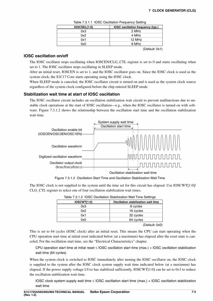
7 ClOCK GeneRaTOR (ClG)
S1C17555/565/955/965 TeChniCal Manual Seiko epson Corporation 7-3(Rev. 1.0)
3.1.1 IOSC Oscillation Frequency SettingTable 7.iOSCSel[1:0] iOSC oscillation frequency (typ.)
0x3 2 MHz0x2 4 MHz0x1 12 MHz0x0 8 MHz
(Default: 0x1)
iOSC oscillation on/off The IOSC oscillator stops oscillating when IOSCEN/CLG_CTL register is set to 0 and starts oscillating when
set to 1. The IOSC oscillator stops oscillating in SLEEP mode. After an initial reset, IOSCEN is set to 1, and the IOSC oscillator goes on. Since the IOSC clock is used as the
system clock, the S1C17 Core starts operating using the IOSC clock. When SLEEP mode is canceled, the IOSC oscillator circuit is turned on and is used as the system clock source
regardless of the system clock configured before the chip entered SLEEP mode.
Stabilization wait time at start of iOSC oscillation The IOSC oscillator circuit includes an oscillation stabilization wait circuit to prevent malfunctions due to un-
stable clock operations at the start of IOSC oscillation—e.g., when the IOSC oscillator is turned on with soft-ware. Figure 7.3.1.2 shows the relationship between the oscillation start time and the oscillation stabilization wait time.
Oscillation enable bit(IOSCEN/OSC3EN/OSC1EN)
Oscillation waveform
Digitized oscillation waveform
Oscillator output clock(fIOSC/fOSC3/fOSC1)
System supply wait timeOscillation start time
Oscillation stabilization wait time
3.1.2 Oscillation Start Time and Oscillation Stabilization Wait TimeFigure 7.
The IOSC clock is not supplied to the system until the time set for this circuit has elapsed. Use IOSCWT[1:0]/CLG_CTL register to select one of four oscillation stabilization wait times.
3.1.2 IOSC Oscillation Stabilization Wait Time SettingsTable 7.
iOSCWT[1:0] Oscillation stabilization wait time
0x3 8 cycles0x2 16 cycles0x1 32 cycles0x0 64 cycles
(Default: 0x0)
This is set to 64 cycles (IOSC clock) after an initial reset. This means the CPU can start operating when the CPU operation start time at initial reset indicated below (at a maximum) has elapsed after the reset state is can-celed. For the oscillation start time, see the “Electrical Characteristics” chapter.
CPU operation start time at initial reset ≤ IOSC oscillation start time (max.) + IOSC oscillation stabilization wait time (64 cycles)
When the system clock is switched to IOSC immediately after turning the IOSC oscillator on, the IOSC clock is supplied to the system after the IOSC clock system supply wait time indicated below (at a maximum) has elapsed. If the power supply voltage LVDD has stabilized sufficiently, IOSCWT[1:0] can be set to 0x3 to reduce the oscillation stabilization wait time.
IOSC clock system supply wait time ≤ IOSC oscillation start time (max.) + IOSC oscillation stabilization wait time

7 ClOCK GeneRaTOR (ClG)
7-4 Seiko epson Corporation S1C17555/565/955/965 TeChniCal Manual (Rev. 1.0)
OSC3 Oscillator [S1C17565/965]7.3.2
The OSC3 oscillator is a high-precision, high-speed oscillator circuit that uses either a crystal resonator or a ceramic resonator. Figure 7.3.2.1 shows the OSC3 oscillator configuration.
A crystal resonator (X’tal3) or a ceramic resonator (Ceramic) and a feedback resistor (Rf3) should be connected between the OSC3 and OSC4 pins. Additionally, two capacitors (CG3 and CD3) should be connected between the OSC3/OSC4 pins and VSS.To use an external clock, leave the OSC4 pin open and input an LVDD-level clock (with a 50% duty cycle) to the OSC3 pin.For the effective frequency range, oscillation characteristics, and external clock input characteristics, see the “Elec-trical Characteristics” chapter.
VSS OSC4
OSC3
OSC4
OSC3
Rf3
CD3
CG3
SLEEP status
X'tal3 orCeramic
fOSC3
OSC3EN
Oscillation stabilization wait circuit
OSC3WT[1:0]
OSC3WCE
SLEEP status
fOSC3
OSC3EN
Oscillation stabilization wait circuit
OSC3WT[1:0]
OSC3WCEN.C.
VSS
LVDD
Externalclock
(1) Crystal/ceramic oscillator circuit
(2) External clock input
3.2.1 OSC3 Oscillator CircuitFigure 7.
OSC3 oscillation on/off The OSC3 oscillator circuit starts oscillating when OSC3EN/CLG_CTL register is set to 1 and stops oscillating
when it is set to 0. The OSC3 oscillator circuit also stops oscillating in SLEEP mode. After an initial reset, OSC3EN is set to 0, and the OSC3 oscillator circuit is halted.
Stabilization wait time at start of OSC3 oscillation The OSC3 oscillator circuit includes an oscillation stabilization wait circuit to prevent malfunctions due to unsta-
ble clock operations at the start of OSC3 oscillation—e.g., when the OSC3 oscillator is turned on with software. The OSC3 clock is not supplied to the system until the time set for this circuit has elapsed. Use OSC3WT[1:0]/
CLG_CTL register to select one of four oscillation stabilization wait times.
3.2.1 OSC3 Oscillation Stabilization Wait Time SettingsTable 7.
OSC3WT[1:0] Oscillation stabilization wait time
0x3 128 cycles0x2 256 cycles0x1 512 cycles0x0 1024 cycles
(Default: 0x0) This is set to 1,024 cycles (OSC3 clock) after an initial reset. When the system clock is switched to OSC3 immediately after the OSC3 oscillator circuit is turned on, the
OSC3 clock is supplied to the system after the OSC3 clock system supply wait time indicated below (at a maxi-mum) has elapsed. For the oscillation start time, see the “Electrical Characteristics” chapter.

7 ClOCK GeneRaTOR (ClG)
S1C17555/565/955/965 TeChniCal Manual Seiko epson Corporation 7-5(Rev. 1.0)
OSC3 clock system supply wait time ≤ OSC3 oscillation start time (max.) + OSC3 oscillation sta-bilization wait time
note: Oscillation stability will vary, depending on the resonator and other external components. Carefully consider the OSC3 oscillation stabilization wait time before reducing the time.
The OSC3 oscillation stabilization wait circuit can be enabled or disabled using OSC3WCE/CLG_NFEN register. After an initial reset, the OSC3 oscillation stabilization wait circuit is enabled (OSC3WCE = 1) and it controls the clock supply to the system. When a stabilized external clock is input to the OSC3 pin, setting OSC3WCE to 0 enables the system to start operating without a stabilization wait time.
OSC1 Oscillator7.3.3
The OSC1 oscillator is a high-precision, low-speed oscillator circuit that uses a 32.768 kHz crystal resonator.The OSC1 clock is generally used as the timer operation clock (for the clock timer, stopwatch timer, watchdog tim-er, and 16-bit PWM timer). It can be used as the system clock instead of the OSC3 or IOSC clock to reduce power consumption when no high-speed processing is required. Figure 7.3.3.1 shows the OSC1 oscillator configuration.
OSC1WCE
OSC1WCE
VSS OSC2
OSC1
OSC2
OSC1
Rf1
CD1
CG1
SLEEP status
X'tal1
fOSC1
OSC1EN
Oscillation stabilization wait circuit
SLEEP status
fOSC1
OSC1EN
Oscillation stabilization wait circuit
N.C.
VSS
LVDD
Externalclock
(1) Crystal oscillator circuit
(2) External clock input
3.3.1 OSC1 Oscillator CircuitFigure 7.
A crystal resonator (X’tal1) and a feedback resistor (Rf1) should be connected between the OSC1 and OSC2 pins. Additionally, two capacitors (CG1 and CD1) should be connected between the OSC1/OSC2 pins and VSS.To use an external clock, leave the OSC2 pin open and input an LVDD-level clock (with a 50% duty cycle) to the OSC1 pin.For oscillation characteristics and external clock input characteristics, see the “Electrical Characteristics” chapter.
OSC1 oscillation on/off The OSC1 oscillator stops oscillating when OSC1EN/CLG_CTL register is set to 0 and starts oscillating when
set to 1. The OSC1 oscillator circuit stops oscillating in SLEEP mode. After an initial reset, OSC1EN is set to 0, and the OSC1 oscillator circuit is halted.
Stabilization wait time at start of OSC1 oscillation The OSC1 oscillator includes an oscillation stabilization wait circuit (fixed at 256 cycles) to prevent malfunc-
tions caused by unstable clock operations at the start of OSC1 oscillation—e.g., when the OSC1 oscillator is turned on with software. When the system clock is switched to OSC1 immediately after the OSC1 oscillator circuit is turned on, the OSC1 clock is supplied to the system after the OSC1 clock system supply wait time indicated below (at a maximum) has elapsed. For the oscillation start time, see the “Electrical Characteristics” chapter.

7 ClOCK GeneRaTOR (ClG)
7-6 Seiko epson Corporation S1C17555/565/955/965 TeChniCal Manual (Rev. 1.0)
OSC1 clock system supply wait time ≤ OSC1 oscillation start time (max.) + OSC1 oscillation stabilization wait time (256 cycles)
The OSC1 oscillation stabilization wait circuit can be enabled or disabled using OSC1WCE/CLG_NFEN register. After an initial reset, the OSC1 oscillation stabilization wait circuit is enabled (OSC1WCE = 1) and it controls the clock supply to the system. When a stabilized external clock is input to the OSC1 pin, setting OSC1WCE to 0 enables the system to start operating without a stabilization wait time.
System Clock Switching7.4 The figure below shows the system clock selector.
fIOSC
fOSC3
fOSC1
S1C17565/965
CLKSRC[1:0]
System clock
4.1 System Clock SelectorFigure 7.
The S1C17555/955 has two system clock sources (IOSC and OSC1) and the S1C17565/965 has three system clock sources (IOSC, OSC3, and OSC1). The system clock can be switched using CLKSRC[1:0]/CLG_SRC register. After an initial reset, the S1C17555/565/955/965 starts operating using IOSC as the system clock. When no high-speed processing is required, switch the system clock to OSC1 and stop the high-speed oscillator circuit to reduce current consumption.
4.1 System Clock SelectionTable 7.
ClKSRC[1:0]System clock source
S1C17555/955 S1C17565/965
0x3 Reserved0x2 Reserved OSC30x1 OSC1 OSC10x0 IOSC IOSC
(Default: 0x0)
The following shows system clock switching procedures:
Switching the system clock to OSC3 from iOSC or OSC1 [S1C17565/965]1. Set the OSC3 oscillation stabilization wait time if necessary. (OSC3WT[1:0])2. Disable the OSC3 oscillation stabilization wait circuit when a stabilized external clock is input to the OSC3
pin. (OSC3WCE = 0)3. Turn the OSC3 oscillator on if it is off. (OSC3EN = 1)4. Select the OSC3 clock as the system clock. (CLKSRC[1:0] = 0x2)5. Turn the IOSC or OSC1 oscillator off if peripheral modules and FOUTA/B output circuits have not used the
IOSC or OSC1 clock.
Switching the system clock to OSC1 from iOSC or OSC3 (S1C17565/965)1. Disable the OSC1 oscillation stabilization wait circuit when a stabilized external clock is input to the OSC1
pin. (OSC1WCE = 0)2. Turn the OSC1 oscillator on. (OSC1EN = 1)3. Select the OSC1 clock as the system clock. (CLKSRC[1:0] = 0x1)4. Turn the IOSC or OSC3 oscillator off if peripheral modules and FOUTA/B output circuits have not used the
IOSC or OSC3 clock.
Switching the system clock to iOSC from OSC3 or OSC11. Set the IOSC oscillation stabilization wait time if necessary. (IOSCWT[1:0])2. Turn the IOSC oscillator on if it is off. (IOSCEN = 1)3. Select the IOSC clock as the system clock. (CLKSRC[1:0] = 0x0)4. Turn the OSC3 or OSC1 oscillator off if peripheral modules and FOUTA/B output circuits have not used
the OSC3 or OSC1 clock.
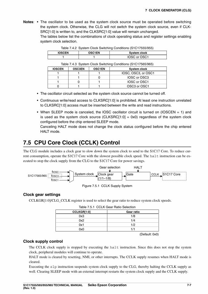
7 ClOCK GeneRaTOR (ClG)
S1C17555/565/955/965 TeChniCal Manual Seiko epson Corporation 7-7(Rev. 1.0)
notes: • The oscillator to be used as the system clock source must be operated before switching the system clock. Otherwise, the CLG will not switch the system clock source, even if CLK-SRC[1:0] is written to, and the CLKSRC[1:0] value will remain unchanged.
The tables below list the combinations of clock operating status and register settings enabling system clock selection.
4.2 System Clock Switching Conditions (S1C17555/955)Table 7.
iOSCen OSC1en System clock
1 1 IOSC or OSC1
4.3 System Clock Switching Conditions (S1C17565/965)Table 7.
iOSCen OSC3en OSC1en System clock
1 1 1 IOSC, OSC3, or OSC11 1 0 IOSC or OSC31 0 1 IOSC or OSC10 1 1 OSC3 or OSC1
• The oscillator circuit selected as the system clock source cannot be turned off.
• Continuous write/read access to CLKSRC[1:0] is prohibited. At least one instruction unrelated to CLKSRC[1:0] access must be inserted between the write and read instructions.
• When SLEEP mode is canceled, the IOSC oscillator circuit is turned on (IOSCEN = 1) and is used as the system clock source (CLKSRC[1:0] = 0x0) regardless of the system clock configured before the chip entered SLEEP mode.
Canceling HALT mode does not change the clock status configured before the chip entered HALT mode.
CPu Core Clock (CClK) Control7.5 The CLG module includes a clock gear to slow down the system clock to send to the S1C17 Core. To reduce cur-rent consumption, operate the S1C17 Core with the slowest possible clock speed. The halt instruction can be ex-ecuted to stop the clock supply from the CLG to the S1C17 Core for power savings.
fIOSC
fOSC3
fOSC1
CCLKClock gear(1/1–1/8)
Gate S1C17 Core
Gear selection
System clock
HALT
S1C17565/965
5.1 CCLK Supply SystemFigure 7.
Clock gear settings CCLKGR[1:0]/CLG_CCLK register is used to select the gear ratio to reduce system clock speeds.
5.1 CCLK Gear Ratio SelectionTable 7.
CClKGR[1:0] Gear ratio
0x3 1/80x2 1/40x1 1/20x0 1/1
(Default: 0x0)
Clock supply control The CCLK clock supply is stopped by executing the halt instruction. Since this does not stop the system
clock, peripheral modules will continue to operate. HALT mode is cleared by resetting, NMI, or other interrupts. The CCLK supply resumes when HALT mode is
cleared. Executing the slp instruction suspends system clock supply to the CLG, thereby halting the CCLK supply as
well. Clearing SLEEP mode with an external interrupt restarts the system clock supply and the CCLK supply.

7 ClOCK GeneRaTOR (ClG)
7-8 Seiko epson Corporation S1C17555/565/955/965 TeChniCal Manual (Rev. 1.0)
Peripheral Module Clock (PClK) Control7.6 The CLG module also controls the clock supply to peripheral modules.The system clock is used unmodified for the peripheral module clock (PCLK).
Internal peripheral modules• UART Ch.0–1• Fine mode 16-bit timer Ch.0–1• 16-bit timer Ch.0–2• 8-bit SPI Ch.0–1• 16-bit SPI• I2C master• I2C slave• Power generator• P port & port MUX• MISC registers• IR remote controller
Gate
On/Off control
PCLKSystem clockfIOSC
fOSC3
fOSC1
S1C17565/965
6.1 Peripheral Module Clock Control CircuitFigure 7.
Clock supply control The PCLK supply is controlled by PCKEN[1:0]/CLG_PCLK register.
6.1 PCLK ControlTable 7.
PCKen[1:0] PClK supply
0x3 Enabled (on)0x2 Setting prohibited0x1 Setting prohibited0x0 Disabled (off)
(Default: 0x3)
The default setting is 0x3, which enables the clock supply. Stop the clock supply to reduce current consumption unless all peripheral modules (modules listed below) within the internal peripheral circuit area need to be run-ning.
note: Do not set PCKEN[1:0]/CLG_PCLK register to 0x2 or 0x1, since doing so will stop the operation of certain peripheral modules.
6.2 Peripheral Modules and Operating ClocksTable 7.Peripheral modules Operating clock Remarks
UART Ch.0 and 1 PCLK The PCLK supply cannot be disabled if one or more peripheral modules in these list must be operated.The PCLK supply can be disabled if all the periph-eral circuits in these list can be stopped.
Fine mode 16-bit timer Ch.0 and 116-bit timer Ch.0 to 28-bit SPI Ch.0 and 116-bit SPII2C masterI2C slavePower generatorP port & port MUXMISC registersIR remote controllerClock timer Divided OSC1 clock The OSC1 oscillator circuit cannot be disabled if
one or more peripheral modules in these list must be operated. The PCLK supply can be disabled.
Stopwatch timer
16-bit PWM timer Ch.0 to 3
Clock selected by software(divided IOSC/OSC3/OSC1 clock)
The oscillator circuit used as the clock source can-not be disabled (see Section 7.7 or each peripheral module chapter). The PCLK supply can be disabled. Watchdog timer
12-bit A/D converterFOUTA/FOUTB outputs

7 ClOCK GeneRaTOR (ClG)
S1C17555/565/955/965 TeChniCal Manual Seiko epson Corporation 7-9(Rev. 1.0)
FSa Clock (FSaClK) Control7.7 The CLG module also controls the clock supply to FSA.The system clock is used unmodified for the FSA clock (FSACLK).
FSAGate
On/Off control
FSACLKSystem clockfIOSC
fOSC3
fOSC1
S1C17565/965
7.1 FSA Clock Control CircuitFigure 7.
Clock supply control The FSACLK supply is controlled by FSACLKEN/CLG_PCLK register. When FSACLKEN is set to 1, FSACLK is supplied to FSA, and it is stopped when set to 0. The default setting is 1, which enables the clock supply. Stop the clock supply to reduce current consumption
unless FSA needs to be running.
note: Set FSACLKEN to 0 even in the S1C17555/565 that does not include FSA, as unnecessary cir-cuits will be operated.
Clock external Output (FOuTa, FOuTB)7.8 A divided IOSC/OSC3 clock or the OSC1 clock can be output to external devices.
I/O port (FOUTA pin)
Divider(1/1–1/4)OSC3 clock
FOUTAoutput circuit
On/Offcontrol
Clock sourceselection
On/Offcontrol
Clock sourceselection
FOUTA division ratio selection
FOUTB division ratio selection
Divider(1/1–1/4)IOSC clock
OSC1 clock
I/O port (FOUTB pin)FOUTBoutput circuit
S1C17565/965
8.1 Clock Output CircuitFigure 7.
There are two output systems available: FOUTA and FOUTB. The FOUTA and FOUTB output circuits have the same functions.
Output pin setting The FOUTA and FOUTB output pins are shared with I/O ports. The pin is configured for the I/O port by de-
fault, so the pin function should be changed using the port function select bit before the clock output can be used. See the “I/O Ports (P)” chapter for the FOUTA/FOUTB pins and selecting pin functions.
Clock source selection The clock source can be selected from IOSC, OSC3, and OSC1 using FOUTASRC[1:0]/CLG_FOUTA register
or FOUTBSRC[1:0]/CLG_FOUTB register.
8.1 Clock Source SelectionTable 7.
FOuTaSRC[1:0]/FOuTBSRC[1:0]
Clock sourceS1C17555/955 S1C17565/965
0x3 Reserved0x2 Reserved OSC30x1 OSC1 OSC10x0 IOSC IOSC
(Default: 0x0)

7 ClOCK GeneRaTOR (ClG)
7-10 Seiko epson Corporation S1C17555/565/955/965 TeChniCal Manual (Rev. 1.0)
Clock frequency selection Three different clock output frequencies can be selected when OSC3 or IOSC is used as the clock source. Se-
lect the division ratio for the source clock using FOUTAD[1:0]/CLG_FOUTA register or FOUTBD[1:0]/CLG_FOUTB register.
8.2 IOSC/OSC3 Division Ratio SelectionTable 7.
FOuTaD[1:0]/FOuTBD[1:0] Division ratio
0x3 Reserved0x2 1/40x1 1/20x0 1/1
(Default: 0x0)Clock output control The clock output is controlled using FOUTAE/CLG_FOUTA register or FOUTBE/CLG_FOUTB register. Set-
ting FOUTAE/FOUTBE to 1 outputs the FOUTA/FOUTB clock from the FOUTA/FOUTB pin. Setting it to 0 disables output.
FOUTAE (FOUTBE)
FOUTA (FOUTB) output
0 01
8.2 FOUTA/FOUTB OutputFigure 7.
note: Since the FOUTA/FOUTB signal is not synchronized with FOUTAE/FOUTBE writing, switching output on or off will generate certain hazards.
Control Register Details7.9
9.1 List of CLG RegistersTable 7.
address Register name Function0x5060 CLG_SRC Clock Source Select Register Selects the clock source.0x5061 CLG_CTL Oscillation Control Register Controls oscillation.0x5062 CLG_NFEN Noise Filter Enable Register Turns oscillation stabilization wait circuit/noise filter on/off.0x5064 CLG_FOUTA FOUTA Control Register Controls FOUTA clock output.0x5065 CLG_FOUTB FOUTB Control Register Controls FOUTB clock output. 0x506e CLG_IOSC IOSC Control Register Configures IOSC oscillation frequency.0x5080 CLG_PCLK PCLK and FSA Clock Control Register Controls the PCLK and FSA clock supply.
0x5081 CLG_CCLK CCLK Control Register Configures the CCLK division ratio.
The CLG module registers are described in detail below.
note: When data is written to the registers, the “Reserved” bits must always be written as 0 and not 1.
Clock Source Select Register (ClG_SRC)Register name address Bit name Function Setting init. R/W Remarks
Clock Source Select Register(ClG_SRC)
0x5060(8 bits)
D7–2 – reserved – – – 0 when being read.D1–0 ClKSRC[1:0] System clock source select CLKSRC[1:0] Clock source 0x0 R/W * S1C17565/965
only0x30x20x10x0
reservedOSC3*OSC1IOSC
D[7:2] Reserved
D[1:0] ClKSRC[1:0]: System Clock Source Select Bits Selects the system clock source.

7 ClOCK GeneRaTOR (ClG)
S1C17555/565/955/965 TeChniCal Manual Seiko epson Corporation 7-11(Rev. 1.0)
9.2 System Clock SelectionTable 7.
ClKSRC[1:0]System clock source
S1C17555/955 S1C17565/965
0x3 Reserved0x2 Reserved OSC30x1 OSC1 OSC10x0 IOSC IOSC
(Default: 0x0)
Select IOSC or OSC3 for normal (high-speed) operations. If no high-speed clock is required, OSC1 can be set as the system clock and IOSC and OSC3 stopped to reduce current consumption.
notes: • The oscillator to be used as the system clock source must be operated before switching the system clock. Otherwise, the CLG will not switch the system clock source, even if CLK-SRC[1:0] is written to, and the CLKSRC[1:0] value will remain unchanged.
The tables below list the combinations of clock operating status and register settings en-abling system clock selection.
9.3 System Clock Switching Conditions (S1C17555/955)Table 7.
iOSCen OSC1en System clock
1 1 IOSC or OSC1
9.4 System Clock Switching Conditions (S1C17565/965)Table 7.
iOSCen OSC3en OSC1en System clock
1 1 1 IOSC, OSC3, or OSC11 1 0 IOSC or OSC31 0 1 IOSC or OSC10 1 1 OSC3 or OSC1
• The oscillator circuit selected as the system clock source cannot be turned off.
• Continuous write/read access to CLKSRC[1:0] is prohibited. At least one instruction unre-lated to CLKSRC[1:0] access must be inserted between the write and read instructions.
• When SLEEP mode is canceled, the IOSC oscillator circuit is turned on (IOSCEN = 1) and is used as the system clock source (CLKSRC[1:0] = 0x0) regardless of the system clock configured before the chip entered SLEEP mode.
Canceling HALT mode does not change the clock status configured before the chip entered HALT mode.
Oscillation Control Register (ClG_CTl)Register name address Bit name Function Setting init. R/W Remarks
Oscillation Control Register(ClG_CTl)
0x5061(8 bits)
D7–6 iOSCWT[1:0] IOSC wait cycle select IOSCWT[1:0] Wait cycle 0x0 R/W0x30x20x10x0
8 cycles16 cycles32 cycles64 cycles
D5–4 OSC3WT[1:0] OSC3 wait cycle select OSC3WT[1:0] Wait cycle 0x0 R/W S1C17565/9650x30x20x10x0
128 cycles256 cycles512 cycles
1024 cyclesreserved – – – S1C17555/955
D3 – reserved – – – 0 when being read.D2 iOSCen IOSC enable 1 Enable 0 Disable 1 R/WD1 OSC1en OSC1 enable 1 Enable 0 Disable 0 R/WD0 OSC3en OSC3 enable 1 Enable 0 Disable 0 R/W S1C17565/965
reserved – – – S1C17555/955
D[7:6] iOSCWT[1:0]: iOSC Wait Cycle Select Bits An oscillation stabilization wait time is set to prevent malfunctions due to unstable clock operations at
the start of IOSC oscillation. The IOSC clock is not supplied to the system immediately after IOSC oscillation starts until the time
set here has elapsed.
7 ClOCK GeneRaTOR (ClG)
7-12 Seiko epson Corporation S1C17555/565/955/965 TeChniCal Manual (Rev. 1.0)
9.5 IOSC Oscillation Stabilization Wait Time SettingsTable 7.
iOSCWT[1:0] Oscillation stabilization wait time
0x3 8 cycles0x2 16 cycles0x1 32 cycles0x0 64 cycles
(Default: 0x0)
This is set to 64 cycles (IOSC clock) after an initial reset. This means the CPU can start operating when the CPU operation start time at initial reset indicated below (at a maximum) has elapsed after the reset state is canceled.
CPU operation start time at initial reset ≤ IOSC oscillation start time (max.) + IOSC oscilla-tion stabilization wait time (64 cycles)
When the system clock is switched to IOSC immediately after turning the IOSC oscillator on, the IOSC clock is supplied to the system after the IOSC clock system supply wait time indicated below (at a maximum) has elapsed. If the power supply voltage LVDD has stabilized sufficiently, IOSCWT[1:0] can be set to 0x3 to reduce the oscillation stabilization wait time.
IOSC clock system supply wait time ≤ IOSC oscillation start time (max.) + IOSC oscillation stabilization wait time
D[5:4] Reserved [S1C17555/955] OSC3WT[1:0]: OSC3 Wait Cycle Select Bits [S1C17565/965] An oscillation stabilization wait time is set to prevent malfunctions due to unstable clock operation at
the start of OSC3 oscillation. The OSC3 clock is not supplied to the system immediately after OSC3 oscillation starts—e.g., when
the OSC3 oscillator is turned on with software—until the time set here has elapsed.
9.6 OSC3 Oscillation Stabilization Wait Time SettingsTable 7.
OSC3WT[1:0] Oscillation stabilization wait time
0x3 128 cycles0x2 256 cycles0x1 512 cycles0x0 1024 cycles
(Default: 0x0)
This is set to 1,024 cycles (OSC3 clock) after an initial reset. When the system clock is switched to OSC3 immediately after the OSC3 oscillator circuit is turned on,
the OSC3 clock is supplied to the system after the OSC3 clock system supply wait time indicated below (at a maximum) has elapsed.
OSC3 clock system supply wait time ≤ OSC3 oscillation start time (max.) + OSC3 oscilla-tion stabilization wait time
note: Oscillation stability will vary, depending on the resonator and other external components. Carefully consider the OSC3 oscillation stabilization wait time before reducing the time.
The OSC3 oscillation stabilization wait circuit is enabled only when OSC3WCE/CLG_NFEN register is set to 1 (default).
D3 Reserved
D2 iOSCen: iOSC enable Bit Enables or disables IOSC oscillator operations. 1 (R/W): Enabled (on) (default) 0 (R/W): Disabled (off)
note: The IOSC oscillator cannot be stopped if a condition shown below is met. • When the IOSC clock is being used as the system clock • When WDT is running with IOSC being used as the WDT clock source

7 ClOCK GeneRaTOR (ClG)
S1C17555/565/955/965 TeChniCal Manual Seiko epson Corporation 7-13(Rev. 1.0)
D1 OSC1en: OSC1 enable Bit Enables or disables OSC1 oscillator operations. 1 (R/W): Enabled (on) 0 (R/W): Disabled (off) (default)
When the system clock is switched to OSC1 immediately after the OSC1 oscillator circuit is turned on, the OSC1 clock is supplied to the system after the OSC1 clock system supply wait time indicated below (at a maximum) has elapsed.
OSC1 clock system supply wait time ≤ OSC1 oscillation start time (max.) + OSC1 oscilla-tion stabilization wait time (256 cycles)
note: The OSC1 oscillator cannot be stopped if a condition shown below is met. • When the OSC1 clock is being used as the system clock • When WDT is running with OSC1 being used as the WDT clock source
D0 Reserved [S1C17555/955] OSC3en: OSC3 enable Bit [S1C17565/965] Enables or disables OSC3 oscillator operations. 1 (R/W): Enabled (on) 0 (R/W): Disabled (off) (default)
note: The OSC3 oscillator cannot be stopped if a condition shown below is met. • When the OSC3 clock is being used as the system clock • When WDT is running with OSC3 being used as the WDT clock source
noise Filter enable Register (ClG_nFen)Register name address Bit name Function Setting init. R/W Remarks
noise Filter enable Register(ClG_nFen)
0x5062(8 bits)
D7–6 – reserved – – – 0 when being read.D5 OSC1WCe OSC1 wait cycle enable 1 Enable 0 Disable 1 R/WD4 OSC3WCe OSC3 wait cycle enable 1 Enable 0 Disable 1 R/W S1C17565/965
reserved – – – S1C17555/955D3–0 – reserved – – – 0x2 when being read.
D[7:6] Reserved
D5 OSC1WCe: OSC1 Wait Cycle enable Bit Enables or disables the OSC1 oscillation stabilization wait circuit. 1 (R/W): Enabled (default) 0 (R/W): Disabled
When using the internal OSC1 oscillator circuit, enable the OSC1 oscillation stabilization wait circuit (OSC1WCE = 1). When the OSC1 oscillator circuit is turned on, the OSC1 clock is supplied to the sys-tem after 256 cycles of oscillation stabilization wait time has elapsed.
When a stabilized external clock is input to the OSC1 pin, setting OSC1WCE to 0 enables the system to start operating without a stabilization wait time.
D4 Reserved [S1C17555/955] OSC3WCe: OSC3 Wait Cycle enable Bit [S1C17565/965] Enables or disables the OSC3 oscillation stabilization wait circuit. 1 (R/W): Enabled (default) 0 (R/W): Disabled
When using the internal OSC3 oscillator circuit, enable the OSC3 oscillation stabilization wait circuit (OSC3WCE = 1). When the OSC3 oscillator circuit is turned on, the OSC3 clock is supplied to the sys-tem after the oscillation stabilization wait time set using OSC3WT[1:0]/CLG_CTL register has elapsed.
When a stabilized external clock is input to the OSC3 pin, setting OSC3WCE to 0 enables the system to start operating without a stabilization wait time.
D[3:0] Reserved

7 ClOCK GeneRaTOR (ClG)
7-14 Seiko epson Corporation S1C17555/565/955/965 TeChniCal Manual (Rev. 1.0)
FOuTa Control Register (ClG_FOuTa)Register name address Bit name Function Setting init. R/W Remarks
FOuTa Control Register(ClG_FOuTa)
0x5064(8 bits)
D7–6 – reserved – – – 0 when being read.D5–4 FOuTaD
[1:0]FOUTA clock division ratio select FOUTAD[1:0] Division ratio 0x0 R/W When the clock
source is IOSC or OSC3
0x30x20x10x0
reserved1/41/21/1
D3–2 FOuTaSRC[1:0]
FOUTA clock source select FOUTASRC[1:0] Clock source 0x0 R/W * S1C17565/965 only0x3
0x20x10x0
reservedOSC3*OSC1IOSC
D1 – reserved – – – 0 when being read.D0 FOuTae FOUTA output enable 1 Enable 0 Disable 0 R/W
D[7:6] Reserved
D[5:4] FOuTaD[1:0]: FOuTa Clock Division Ratio Select Bits Selects the clock division ratio to set the FOUTA clock frequency when OSC3 or IOSC is used as the
clock source.
9.7 OSC3/IOSC Division Ratio SelectionTable 7.
FOuTaD[1:0] Division ratio
0x3 Reserved0x2 1/40x1 1/20x0 1/1
(Default: 0x0)
When OSC1 is used as the clock source, FOUTAD[1:0] is ineffective and the OSC1 clock is output without frequency division.
D[3:2] FOuTaSRC[1:0]: FOuTa Clock Source Select Bits Selects the FOUTA clock source.
9.8 FOUTA Clock Source SelectionTable 7.
FOuTaSRC[1:0]Clock source
S1C17555/955 S1C17565/9650x3 Reserved0x2 Reserved OSC30x1 OSC1 OSC10x0 IOSC IOSC
(Default: 0x0)
D1 Reserved
D0 FOuTae: FOuTa Output enable Bit Enables or disables FOUTA clock external output. 1 (R/W): Enabled (on) 0 (R/W): Disabled (off) (default)
Setting FOUTAE to 1 outputs the FOUTA clock from the FOUTA pin. Setting it to 0 stops the output.
FOuTB Control Register (ClG_FOuTB)Register name address Bit name Function Setting init. R/W Remarks
FOuTB Control Register(ClG_FOuTB)
0x5065(8 bits)
D7–6 – reserved – – – 0 when being read.D5–4 FOuTBD
[1:0]FOUTB clock division ratio select FOUTBD[1:0] Division ratio 0x0 R/W When the clock
source is IOSC or OSC3
0x30x20x10x0
reserved1/41/21/1
D3–2 FOuTBSRC[1:0]
FOUTB clock source select FOUTBSRC[1:0] Clock source 0x0 R/W * S1C17565/965 only0x3
0x20x10x0
reservedOSC3*OSC1IOSC
D1 – reserved – – – 0 when being read.D0 FOuTBe FOUTB output enable 1 Enable 0 Disable 0 R/W

7 ClOCK GeneRaTOR (ClG)
S1C17555/565/955/965 TeChniCal Manual Seiko epson Corporation 7-15(Rev. 1.0)
D[7:6] Reserved
D[5:4] FOuTBD[1:0]: FOuTB Clock Division Ratio Select Bits Selects the clock division ratio to set the FOUTB clock frequency when OSC3 or IOSC is used as the
clock source.
9.9 OSC3/IOSC Division Ratio SelectionTable 7.FOuTBD[1:0] Division ratio
0x3 Reserved0x2 1/40x1 1/20x0 1/1
(Default: 0x0)
When OSC1 is used as the clock source, FOUTBD[1:0] is ineffective and the OSC1 clock is output without frequency division.
D[3:2] FOuTBSRC[1:0]: FOuTB Clock Source Select Bits Selects the FOUTB clock source.
9.10 FOUTB Clock Source SelectionTable 7.
FOuTBSRC[1:0]Clock source
S1C17555/955 S1C17565/9650x3 Reserved0x2 Reserved OSC30x1 OSC1 OSC10x0 IOSC IOSC
(Default: 0x0)
D1 Reserved
D0 FOuTBe: FOuTB Output enable Bit Enables or disables FOUTB clock external output. 1 (R/W): Enabled (on) 0 (R/W): Disabled (off) (default)
Setting FOUTBE to 1 outputs the FOUTB clock from the FOUTB pin. Setting it to 0 stops the output.
iOSC Control Register (ClG_iOSC)Register name address Bit name Function Setting init. R/W Remarks
iOSC Control Register(ClG_iOSC)
0x506e(8 bits)
D7–2 – reserved – – – 0 when being read.D1–0 iOSCSel
[1:0]IOSC frequency select IOSCSEL[1:0] Frequency 0x1 R/W
0x30x20x10x0
2 MHz4 MHz
12 MHz8 MHz
D[7:2] Reserved
D[1:0] iOSCSel[1:0]: iOSC Frequency Select Bits Selects the IOSC oscillation frequency.
9.11 IOSC Oscillation Frequency SettingTable 7.iOSCSel[1:0] iOSC oscillation frequency (typ.)
0x3 2 MHz0x2 4 MHz0x1 12 MHz0x0 8 MHz
(Default: 0x1)

7 ClOCK GeneRaTOR (ClG)
7-16 Seiko epson Corporation S1C17555/565/955/965 TeChniCal Manual (Rev. 1.0)
PClK and FSa Clock Control Register (ClG_PClK)Register name address Bit name Function Setting init. R/W Remarks
PClK and FSa Clock Control Register(ClG_PClK)
0x5080(8 bits)
D7–5 – reserved – – – 0 when being read.D4 FSaCKen FSACLK enable 1 Enable 0 Disable 1 R/W
D3–2 – reserved – – – 0 when being read.D1–0 PCKen[1:0] PCLK enable PCKEN[1:0] PCLK supply 0x3 R/W
0x30x20x10x0
EnableNot allowedNot allowed
Disable
D[7:5] Reserved
D4 FSaCKen: FSaClK enable Bit Enables or disables clock (FSACLK) supply to FSA. 1 (R/W): Enabled (on) (default) 0 (R/W): Disabled (off)
D[3:2] Reserved
D[1:0] PCKen[1:0]: PClK enable Bits Enables or disables clock (PCLK) supply to the internal peripheral modules.
9.12 PCLK ControlTable 7.
PCKen[1:0] PClK supply
0x3 Enabled (on)0x2 Setting prohibited0x1 Setting prohibited0x0 Disabled (off)
(Default: 0x3)
The PCKEN[1:0] default setting is 0x3, which enables clock supply.
Peripheral modules that use PCLK • UART Ch.0 and 1 • Fine mode 16-bit timer Ch.0 and 1 • 16-bit timer Ch.0 to 2 • 8-bit SPI Ch.0 and 1 • 16-bit SPI • I2C master • I2C slave • Power generator • P port & port MUX • MISC registers • IR remote controller
The PCLK supply cannot be disabled if one or more peripheral modules in these list must be oper-ated. The PCLK supply can be disabled if all the peripheral circuits in these list can be stopped.
Stop the PCLK supply to reduce current consumption if all the peripheral modules listed above are not required.
Peripheral modules/functions that do not use PCLK • Clock timer • Stopwatch timer • Watchdog timer • 16-bit PWM timer Ch.0 to 3 • 12-bit A/D converter • FOUTA/FOUTB outputs • FSA
These peripheral modules/functions can operate even if PCLK is stopped.
note: Do not set PCKEN[1:0] to 0x2 or 0x1, since doing so will stop the operation of certain periph-eral modules.

7 ClOCK GeneRaTOR (ClG)
S1C17555/565/955/965 TeChniCal Manual Seiko epson Corporation 7-17(Rev. 1.0)
CClK Control Register (ClG_CClK)Register name address Bit name Function Setting init. R/W Remarks
CClK Control Register(ClG_CClK)
0x5081(8 bits)
D7–2 – reserved – – – 0 when being read.D1–0 CClKGR[1:0] CCLK clock gear ratio select CCLKGR[1:0] Gear ratio 0x0 R/W
0x30x20x10x0
1/81/41/21/1
D[7:2] Reserved
D[1:0] CClKGR[1:0]: CClK Clock Gear Ratio Select Bits Selects the gear ratio for reducing system clock speed and sets the CCLK clock speed for operating the
S1C17 Core. To reduce current consumption, operate the S1C17 Core using the slowest possible clock speed.
9.13 CCLK Gear Ratio SelectionTable 7.
CClKGR[1:0] Gear ratio
0x3 1/80x2 1/40x1 1/20x0 1/1
(Default: 0x0)

8 i/O PORTS (P)
S1C17555/565/955/965 TeChniCal Manual Seiko epson Corporation 8-1(Rev. 1.0)
I/O Ports (P)8
P Module Overview8.1 The P ports are general-purpose digital inputs/outputs that allow software to control the input/output direction, pull-up resistor, and input interface level. Each port can generate interrupts caused by a transition of the input signal. These ports are shared with internal peripheral module inputs/outputs, and the pin functions can be switched by set-ting the registers.The following shows the features of the P module:
• S1C17565/965 Maximum 24 I/O ports (P0[7:0], P1[7:0], P2[7:0]) are available.
S1C17555/955 Maximum 20 I/O ports (P0[7:0], P1[7:0], P2[3:0]) are available.
* The number of ports for general-purpose use depends on the peripheral functions used.
• Each port has a pull-up resistor that can be enabled with software.
• Each port can generate input interrupts at the signal edge selected with software.
• Each port includes a chattering filter.
• Can generate an initial reset by entering low level simultaneously to the P0 ports selected with software.
• All port provide a port function select bit to configure the pin function (for GPIO or peripheral functions).
Figure 8.1.1 shows the I/O port configuration.
Peripheral output
Peripheral I/O control
PxPUy
PxOENy
PxOUTy
PxyMUX
Pull-up enable
Output enable
Output data
Function selection
HVDD
VSSInte
rnal
dat
a bu
s
Pxy
Peripheral module input
PxIENy
PxCF1[2:0]/PxCF2[2:0]
Chattering filter
Input enable
1.1 I/O Port ConfigurationFigure 8.
notes: • The PCLK clock must be supplied from the clock generator to access the I/O port. The PCLK clock is also needed to operate the chattering filters.
• The “xy” in the register and bit names refers to the port number (Pxy, x = 0 to 2, y = 0 to 7). Example: PxINy/Px_IN register P00: P0IN0/P0_IN register P17: P1IN7/P1_IN register
8 i/O PORTS (P)
8-2 Seiko epson Corporation S1C17555/565/955/965 TeChniCal Manual (Rev. 1.0)
input/Output Pin Function Selection (Port MuX)8.2 The I/O port pins share peripheral module input/output pins. Each pin can be configured for use as an I/O port or for a peripheral module function via the corresponding port function-select bits. Pins not used for peripheral mod-ules can be used as general-purpose I/O ports.
2.1 Input/Output Pin Function SelectionTable 8.
Pin function 1PxyMuX[1:0] = 0x0
Pin function 2PxyMuX[1:0] = 0x1
Pin function 3PxyMuX[1:0] = 0x2
Pin function 4 PxyMuX[1:0] = 0x3
Port function select bits
P00 SDI0 (SPI) – – P00MUX[1:0]/P00_03PMUX registerP01 SDO0 (SPI) SCLM (I2CM) SCLS (I2CS) P01MUX[1:0]/P00_03PMUX registerP02 SPICLK0 (SPI) SDAM (I2CM) SDAS (I2CS) P02MUX[1:0]/P00_03PMUX registerP03 #SPISS0 (SPI) – – P03MUX[1:0]/P00_03PMUX registerP04 SIN0 (UART) – – P04MUX[1:0]/P04_07PMUX registerP05 SOUT0 (UART) – – P05MUX[1:0]/P04_07PMUX registerP06 SCLK0 (UART) FOUTA (CLG) #BFR (I2CS) P06MUX[1:0]/P04_07PMUX registerP07 SCLM (I2CM) SCLS (I2CS) – P07MUX[1:0]/P04_07PMUX registerP10 SDAM (I2CM) SDAS (I2CS) – P10MUX[1:0]/P10_13PMUX registerP11 SDI1 (SPI) TOUTA1/CAPA1 (T16A2) – P11MUX[1:0]/P10_13PMUX registerP12 (EXCL0) SDO1 (SPI) – – P12MUX[1:0]/P10_13PMUX registerP13 (EXCL1) SPICLK1 (SPI) – – P13MUX[1:0]/P10_13PMUX registerP14 #SPISS1 (SPI) TOUTA0/CAPA0 (T16A2) – P14MUX[1:0]/P14_17PMUX registerP15 (MSCLK) – – – P15MUX[1:0]/P14_17PMUX registerDSIO (DBG) P16 – – P16MUX[1:0]/P14_17PMUX registerDST2 (DBG) P17 – – P17MUX[1:0]/P14_17PMUX registerP20 SDI2 (SPI16) TOUTA2/CAPA2 (T16A2) – P20MUX[1:0]/P20_23PMUX registerP21 SDO2 (SPI16) FOUTB (CLG) – P21MUX[1:0]/P20_23PMUX registerP22 SPICLK2 (SPI16) REMI (REMC)* – P22MUX[1:0]/P20_23PMUX registerP23 (EXCL2) SPISS2 (SPI16) SCLK1 (UART)* – P23MUX[1:0]/P20_23PMUX registerP24* SIN1 (UART)* TOUTA3/CAPA3 (T16A2)* – P24MUX[1:0]/P24_27PMUX registerP25* SOUT1 (UART)* REMO (REMC)* – P25MUX[1:0]/P24_27PMUX registerP26* SCLM (I2CM)* SCLS (I2CS)* – P26MUX[1:0]/P24_27PMUX registerP27* SDAM (I2CM)* SDAS (I2CS)* – P27MUX[1:0]/P24_27PMUX register
* Available only for the S1C17565/965
At initial reset, each I/O port pin (Pxy) is initialized for the default function (“Pin function 1” in Table 8.2.1).
Pins P12, P13, and P23 can also be used as the 16-bit PWM timer external clock input pins by setting them to input mode. The P15 pin can also be used as the 12-bit A/D converter external clock input pin by setting them to input mode. However, general-purpose input port function is also effective in this case.
For information on functions other than the I/O ports, see the descriptions of the peripheral modules indicated in parentheses. The sections below describe port functions with the pins set as general-purpose I/O ports.
Data input/Output8.3
Data input/output control The I/O ports allow selection of the data input/output direction for each bit using PxOENy/Px_OEN register and
PxIENy/Px_IEN register. PxOENy enables and disables data output, while PxIENy enables and disables data input.
3.1 Data Input/Output StatusTable 8.
PxOenyoutput control
Pxienyinput control
PxPuypull-up control
Port status
0 1 0 Functions as an input port (pull-up off).The port pin (external input signal) value can be read out from PxINy (input data). Output is disabled.
0 1 1 Functions as an input port (pull-up on). (Default)The port pin (external input signal) value can be read out from PxINy (input data). Output is disabled.
1 0 1 or 0 Functions as an output port (pull-up off).Input is disabled. The value read from PxINy (input data) is 0.

8 i/O PORTS (P)
S1C17555/565/955/965 TeChniCal Manual Seiko epson Corporation 8-3(Rev. 1.0)
PxOenyoutput control
Pxienyinput control
PxPuypull-up control
Port status
1 1 1 or 0 Functions as an output port (pull-up off).Input is also enabled. The port pin value (output value) can be read out from PxINy (input data).
0 0 0 The pin is placed into high-impedance status (pull-up off).Output and input are both disabled. The value read from PxINy (input data) is 0.
0 0 1 The pin is placed into high-impedance status (pull-up on).Output and input are both disabled. The value read from PxINy (input data) is 0.
The input/output direction of ports with a peripheral module function selected is controlled by the peripheral module. PxOENy and PxIENy settings are ignored.
Data input To input the port pin status and read out the value, enable input by setting PxIENy to 1 (default). To input an external signal, PxOENy should also be set to 0 (default). The I/O port is placed into high-imped-
ance status and it functions as an input port (input mode). The port is pulled up if pull-up is enabled by PxPUy/Px_PU register.
In input mode, the input pin status can be read out directly from PxINy/Px_IN register. The value read will be 1 when the input pin is at High (HVDD) level and 0 when it is at Low (VSS) level.
The port pin status is always input when PxIENy is 1, even if output is enabled (PxOENy = 1) (output mode). In this case, the value actually output from the port can be read out from PxINy.
When PxIENy is set to 0, input is disabled, and 0 will be read out from PxINy.
Data output To output data from the port pin, enable output by setting PxOENy to 1 (set to output mode). The I/O port then
functions as an output port, and the value set in the PxOUTy/Px_OUT register is output from the port pin. The port pin outputs High (HVDD) level when PxOUTy is set to 1 and Low (VSS) level when set to 0. Note that the port will not be pulled up in output mode, even if pull-up is enabled by PxPUy.
Writing to PxOUTy is possible without affecting pin status, even in input mode.
Pull-up Control8.4 The I/O port contains a pull-up resistor that can be enabled or disabled individually for each bit using PxPUy/Px_PU register. Setting PxPUy to 1 (default) enables the pull-up resistor and pulls up the port pin in input mode. It will not be pulled up if set to 0. The PxPUy setting is ignored and not pulled up in output mode, regardless of how the PxIENy is set.I/O ports that are not used should be set with pull-up enabled.This pull-up setting is also enabled for ports for which the peripheral module function has been selected.A delay will occur in the waveform rising edge depending on time constants such as pull-up resistance and pin load capacitance if the port pin is switched from Low level to High level through the internal pull-up resistor. An ap-propriate wait time must be set for the I/O port loading. The wait time set should be a value not less than that calcu-lated from the following equation.
Wait time = RIN × (CIN + load capacitance on board) × 1.6 [s] RIN: pull-up resistance maximum value, CIN: pin capacitance maximum value
Chattering Filter Function8.5 The I/O ports include a chattering filter circuit for key entry that can be disabled or enabled with a check time spec-ified individually for the four Px[3:0] and Px[7:4] ports using PxCF1[2:0]/Px_CHAT register and PxCF2[2:0]/Px_CHAT register, respectively.
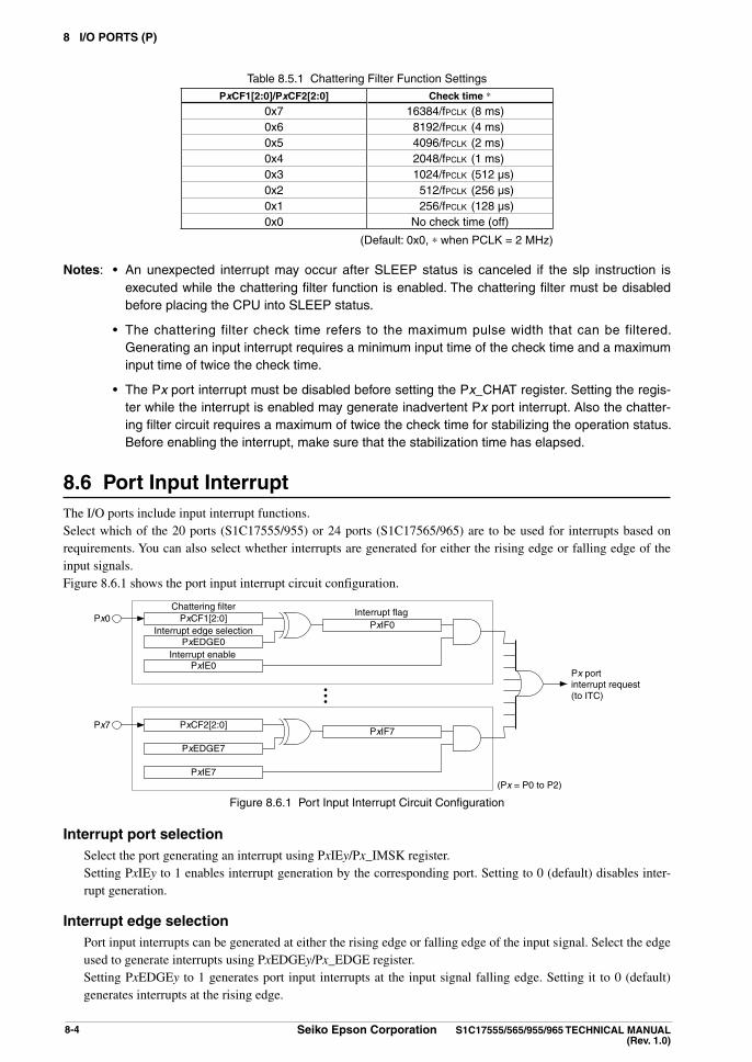
8 i/O PORTS (P)
8-4 Seiko epson Corporation S1C17555/565/955/965 TeChniCal Manual (Rev. 1.0)
5.1 Chattering Filter Function SettingsTable 8.
PxCF1[2:0]/PxCF2[2:0] Check time *
0x7 16384/fPCLK (8 ms)0x6 8192/fPCLK (4 ms)0x5 4096/fPCLK (2 ms)0x4 2048/fPCLK (1 ms)0x3 1024/fPCLK (512 µs)0x2 512/fPCLK (256 µs)0x1 256/fPCLK (128 µs)0x0 No check time (off)
(Default: 0x0, * when PCLK = 2 MHz)
notes: • An unexpected interrupt may occur after SLEEP status is canceled if the slp instruction is executed while the chattering filter function is enabled. The chattering filter must be disabled before placing the CPU into SLEEP status.
• The chattering filter check time refers to the maximum pulse width that can be filtered. Generating an input interrupt requires a minimum input time of the check time and a maximum input time of twice the check time.
• The Px port interrupt must be disabled before setting the Px_CHAT register. Setting the regis-ter while the interrupt is enabled may generate inadvertent Px port interrupt. Also the chatter-ing filter circuit requires a maximum of twice the check time for stabilizing the operation status. Before enabling the interrupt, make sure that the stabilization time has elapsed.
Port input interrupt8.6 The I/O ports include input interrupt functions.Select which of the 20 ports (S1C17555/955) or 24 ports (S1C17565/965) are to be used for interrupts based on requirements. You can also select whether interrupts are generated for either the rising edge or falling edge of the input signals.Figure 8.6.1 shows the port input interrupt circuit configuration.
Px portinterrupt request(to ITC)
(Px = P0 to P2)
Chattering filterInterrupt flag
Interrupt enable
Interrupt edge selectionPx0 PxCF1[2:0]
PxEDGE0
PxIF0
PxIE0
Px7 PxCF2[2:0]
PxEDGE7
PxIF7
PxIE7
• •
•
6.1 Port Input Interrupt Circuit ConfigurationFigure 8.
interrupt port selection Select the port generating an interrupt using PxIEy/Px_IMSK register. Setting PxIEy to 1 enables interrupt generation by the corresponding port. Setting to 0 (default) disables inter-
rupt generation.
interrupt edge selection Port input interrupts can be generated at either the rising edge or falling edge of the input signal. Select the edge
used to generate interrupts using PxEDGEy/Px_EDGE register. Setting PxEDGEy to 1 generates port input interrupts at the input signal falling edge. Setting it to 0 (default)
generates interrupts at the rising edge.

8 i/O PORTS (P)
S1C17555/565/955/965 TeChniCal Manual Seiko epson Corporation 8-5(Rev. 1.0)
interrupt flags The ITC is able to accept three interrupt requests from the P0–P2 ports, and the P port module contains inter-
rupt flags PxIFy/Px_IFLG register corresponding to the individual 24 ports to enable individual control of the 24 Pxy port interrupts. PxIFy is set to 1 at the specified edge (rising or falling edge) of the input signal. If the corresponding PxIEy has been set to 1, an interrupt request signal is also output to the ITC at the same time. An interrupt is generated if the ITC and S1C17 Core interrupt conditions are satisfied.
PxIFy is reset by writing 1. For specific information on interrupt processing, see the “Interrupt Controller (ITC)” chapter.
notes: • The P port module interrupt flag PxIFy must be reset in the interrupt handler routine after a port interrupt has occurred to prevent recurring interrupts.
• To prevent generating unnecessary interrupts, reset the relevant PxIFy before enabling inter-rupts for the required port using PxIEy.
P0 Port Key-entry Reset 8.7 Entering low level simultaneously to the ports (P00–P03) selected with software triggers an initial reset. The ports used for the reset function can be selected with the P0KRST[1:0]/P0_KRST register.
7.1 Configuration of P0 Port Key-Entry ResetTable 8.
P0KRST[1:0] Port used for resetting
0x3 P00, P01, P02, P030x2 P00, P01, P020x1 P00, P010x0 Not used
(Default: 0x0)
For example, if P0KRST[1:0] is set to 0x3, an initial reset will take place when the four ports P00–P03 are set to low level at the same time.
note: The P0 port key-entry reset function cannot be used for power-on reset as it must be enabled with software.
Control Register Details8.8
8.1 List of I/O Port Control RegistersTable 8.
address Register name Function0x5200 P0_IN P0 Port Input Data Register P0 port input data0x5201 P0_OUT P0 Port Output Data Register P0 port output data0x5202 P0_OEN P0 Port Output Enable Register Enables P0 port outputs.0x5203 P0_PU P0 Port Pull-up Control Register Controls the P0 port pull-up resistor.0x5205 P0_IMSK P0 Port Interrupt Mask Register Enables P0 port interrupts.0x5206 P0_EDGE P0 Port Interrupt Edge Select Register Selects the signal edge for generating P0 port interrupts.0x5207 P0_IFLG P0 Port Interrupt Flag Register Indicates/resets the P0 port interrupt occurrence status.0x5208 P0_CHAT P0 Port Chattering Filter Control Register Controls the P0 port chattering filter.0x5209 P0_KRST P0 Port Key-Entry Reset Configuration Register Configures the P0 port key-entry reset function.0x520a P0_IEN P0 Port Input Enable Register Enables P0 port inputs.0x5210 P1_IN P1 Port Input Data Register P1 port input data0x5211 P1_OUT P1 Port Output Data Register P1 port output data0x5212 P1_OEN P1 Port Output Enable Register Enables P1 port outputs.0x5213 P1_PU P1 Port Pull-up Control Register Controls the P1 port pull-up resistor.0x5215 P1_IMSK P1 Port Interrupt Mask Register Enables P1 port interrupts.0x5216 P1_EDGE P1 Port Interrupt Edge Select Register Selects the signal edge for generating P1 port interrupts.0x5217 P1_IFLG P1 Port Interrupt Flag Register Indicates/resets the P1 port interrupt occurrence status.0x5218 P1_CHAT P1 Port Chattering Filter Control Register Controls the P1 port chattering filter.0x521a P1_IEN P1 Port Input Enable Register Enables P1 port inputs.0x5220 P2_IN P2 Port Input Data Register P2 port input data0x5221 P2_OUT P2 Port Output Data Register P2 port output data0x5222 P2_OEN P2 Output Enable Register Enables P2 port outputs.0x5223 P2_PU P2 Port Pull-up Control Register Controls the P2 port pull-up resistor.

8 i/O PORTS (P)
8-6 Seiko epson Corporation S1C17555/565/955/965 TeChniCal Manual (Rev. 1.0)
address Register name Function0x5225 P2_IMSK P2 Port Interrupt Mask Register Enables P2 port interrupts.0x5226 P2_EDGE P2 Port Interrupt Edge Select Register Selects the signal edge for generating P2 port interrupts.0x5227 P2_IFLG P2 Port Interrupt Flag Register Indicates/resets the P2 port interrupt occurrence status.0x5228 P2_CHAT P2 Port Chattering Filter Control Register Controls the P2 port chattering filter.0x522a P2_IEN P2 Port Input Enable Register Enables P2 port inputs.0x52a0 P00_03PMUX P0[3:0] Port Function Select Register Selects the P0[3:0] port functions. 0x52a1 P04_07PMUX P0[7:4] Port Function Select Register Selects the P0[7:4] port functions. 0x52a2 P10_13PMUX P1[3:0] Port Function Select Register Selects the P1[3:0] port functions. 0x52a3 P14_17PMUX P1[7:4] Port Function Select Register Selects the P1[7:4] port functions. 0x52a4 P20_23PMUX P2[3:0] Port Function Select Register Selects the P2[3:0] port functions.0x52a5 P24_27PMUX P2[7:4] Port Function Select Register Selects the P2[7:4] port functions. *
* Available only for the S1C17565/965
The I/O port registers are described in detail below.
note: When data is written to the registers, the “Reserved” bits must always be written as 0 and not 1.
Px Port input Data Registers (Px_in)Register name address Bit name Function Setting init. R/W Remarks
Px Port input Data Register(Px_in)
0x52000x52100x5220(8 bits)
D7–0 Pxin[7:0] Px[7:0] port input data 1 1 (H) 0 0 (L) × R
* The P2IN[7:4] bits are available only for the S1C17565/965.
D[7:0] Pxin[7:0]: Px[7:0] Port input Data Bits The port pin status can be read out. (Default: external input status) 1 (R): High level 0 (R): Low level
PxINy corresponds directly to the Pxy pin. The pin voltage level can be read out when input is enabled (PxIENy = 1) (even if output is also enabled (PxOENy = 1)). The value read out will be 1 when the pin voltage is High and 0 when Low.
The value read out is 0 when input is disabled (PxIENy = 0). Writing operations to the read-only PxINy is disabled.
Px Port Output Data Registers (Px_OuT)Register name address Bit name Function Setting init. R/W Remarks
Px Port Output Data Register(Px_OuT)
0x52010x52110x5221(8 bits)
D7–0 PxOuT[7:0] Px[7:0] port output data 1 1 (H) 0 0 (L) 0 R/W
* The P2OUT[7:4] bits are available only for the S1C17565/965.
D[7:0] PxOuT[7:0]: Px[7:0] Port Output Data Bits Sets the data to be output from the port pin. 1 (R/W): High level 0 (R/W): Low level (default)
PxOUTy corresponds directly to the Pxy pins. The data written will be output unchanged from the port pins when output is enabled (PxOENy = 1). The port pin will be High when the data bit is set to 1 and Low when set to 0.
Port data can also be written when output is disabled (PxOENy = 0) (the pin status is unaffected).
Px Port Output enable Registers (Px_Oen)Register name address Bit name Function Setting init. R/W Remarks
Px Port Output enable Register(Px_Oen)
0x52020x52120x5222(8 bits)
D7–0 PxOen[7:0] Px[7:0] port output enable 1 Enable 0 Disable 0 R/W
* The P2OEN[7:4] bits are available only for the S1C17565/965.

8 i/O PORTS (P)
S1C17555/565/955/965 TeChniCal Manual Seiko epson Corporation 8-7(Rev. 1.0)
D[7:0] PxOen[7:0]: Px[7:0] Port Output enable Bits Enables or disables port outputs. 1 (R/W): Enabled 0 (R/W): Disabled (default)
PxOENy is the output enable bit that corresponds directly to Pxy port. Setting to 1 enables output and the data set in PxOUTy is output from the port pin. Output is disabled when PxOENy is set to 0, and the port pin is set into high-impedance status. The peripheral module determines whether output is enabled or disabled when the port is used for a peripheral module function.
Refer to Table 8.3.1 for more information on input/output status for ports, including settings other than for the PxOEN register.
Px Port Pull-up Control Registers (Px_Pu)Register name address Bit name Function Setting init. R/W Remarks
Px Port Pull-up Control Register(Px_Pu)
0x52030x52130x5223(8 bits)
D7–0 PxPu[7:0] Px[7:0] port pull-up enable 1 Enable 0 Disable 1(0xff)
R/W
* The P2PU[7:4] bits are available only for the S1C17565/965.
D[7:0] PxPu[7:0]: Px[7:0] Port Pull-up enable Bits Enables or disables the pull-up resistor included in each port. 1 (R/W): Enabled (default) 0 (R/W): Disabled
PxPUy is the pull-up control bit that corresponds directly to the Pxy port. Setting to 1 enables the pull-up resistor and the port pin will be pulled up when output is disabled (PxOENy = 0). When PxPUy is set to 0, the pin will not be pulled up.
When output is enabled (PxOENy = 1), the PxPUy setting is ignored, and the pin is not pulled up. I/O ports that are not used should be set with pull-up enabled. This pull-up setting is also enabled for ports for which the peripheral module input function is selected.
Px Port interrupt Mask Registers (Px_iMSK)Register name address Bit name Function Setting init. R/W Remarks
Px Port interrupt Mask Register(Px_iMSK)
0x52050x52150x5225(8 bits)
D7–0 Pxie[7:0] Px[7:0] port interrupt enable 1 Enable 0 Disable 0 R/W
* The P2IE[7:4] bits are available only for the S1C17565/965.
D[7:0] Pxie[7:0]: Px[7:0] Port interrupt enable Bits Enables or disables each port interrupt. 1 (R/W): Interrupt enabled 0 (R/W): Interrupt disabled (default)
Setting PxIEy to 1 enables the corresponding Pxy port input interrupt, while setting to 0 disables the in-terrupt. Status changes for the input pins with interrupt disabled do not affect interrupt occurrence.
Px Port interrupt edge Select Registers (Px_eDGe)Register name address Bit name Function Setting init. R/W Remarks
Px Port interrupt edge Select Register(Px_eDGe)
0x52060x52160x5226(8 bits)
D7–0 PxeDGe[7:0] Px[7:0] port interrupt edge select 1 Falling edge 0 Rising edge 0 R/W
* The P2EDGE[7:4] bits are available only for the S1C17565/965.
D[7:0] PxeDGe[7:0]: Px[7:0] Port interrupt edge Select Bits Selects the input signal edge for generating each port interrupt. 1 (R/W): Falling edge 0 (R/W): Rising edge (default)
Port interrupts are generated at the input signal falling edge when PxEDGEy is set to 1 and at the rising edge when set to 0.

8 i/O PORTS (P)
8-8 Seiko epson Corporation S1C17555/565/955/965 TeChniCal Manual (Rev. 1.0)
Px Port interrupt Flag Registers (Px_iFlG)Register name address Bit name Function Setting init. R/W Remarks
Px Port interrupt Flag Register(Px_iFlG)
0x52070x52170x5227(8 bits)
D7–0 PxiF[7:0] Px[7:0] port interrupt flag 1 Cause of interrupt occurred
0 Cause of interrupt not occurred
0 R/W Reset by writing 1.
* The P2IF[7:4] bits are available only for the S1C17565/965.
D[7:0] PxiF[7:0]: Px[7:0] Port interrupt Flag Bits These are interrupt flags indicating the interrupt cause occurrence status. 1 (R): Interrupt cause occurred 0 (R): No interrupt cause occurred (default) 1 (W): Reset flag 0 (W): Ignored
PxIFy is the interrupt flag that corresponds directly to the Pxy port and is set to 1 at the specified edge (rising or falling edge) of the input signal. When the corresponding PxIEy/Px_IMSK register has been set to 1, a port interrupt request signal is also output to the ITC at the same time. An interrupt is gener-ated if the ITC and S1C17 Core interrupt conditions are satisfied.
PxIFy is reset by writing 1.
notes: • The P port module interrupt flag PxIFy must be reset in the interrupt handler routine after a port interrupt has occurred to prevent recurring interrupts.
• To prevent generating unnecessary interrupts, reset the relevant PxIFy before enabling in-terrupts for the required port using PxIEy/Px_IMSK register.
Px Port Chattering Filter Control Registers (Px_ChaT)Register name address Bit name Function Setting init. R/W Remarks
Px Port Chattering Filter Control Register(Px_ChaT)
0x52080x52180x5228(8 bits)
D7 – reserved – – – 0 when being read.D6–4 PxCF2[2:0] Px[7:4] chattering filter time select PxCF2[2:0] Filter time 0x0 R/W
0x70x60x50x40x30x20x10x0
16384/fPCLK
8192/fPCLK
4096/fPCLK
2048/fPCLK
1024/fPCLK
512/fPCLK
256/fPCLK
NoneD3 – reserved – – – 0 when being read.
D2–0 PxCF1[2:0] Px[3:0] chattering filter time select PxCF1[2:0] Filter time 0x0 R/W0x70x60x50x40x30x20x10x0
16384/fPCLK
8192/fPCLK
4096/fPCLK
2048/fPCLK
1024/fPCLK
512/fPCLK
256/fPCLK
None
* The P2CF2[2:0] bits are available only for the S1C17565/965.
D7 Reserved
D[6:4] PxCF2[2:0]: Px[7:4] Chattering Filter Time Select Bits Configures the chattering filter circuit for the Px[7:4] ports.
D3 Reserved
D[2:0] PxCF1[2:0]: Px[3:0] Chattering Filter Time Select Bits Configures the chattering filter circuit for the Px[3:0] ports.
The I/O ports include a chattering filter circuit for key entry that can be disabled or enabled with a check time specified individually for the four Px[3:0] and Px[7:4] ports using PxCF1[2:0] and PxCF2[2:0], respectively.

8 i/O PORTS (P)
S1C17555/565/955/965 TeChniCal Manual Seiko epson Corporation 8-9(Rev. 1.0)
8.2 Chattering Filter Function SettingsTable 8.
PxCF1[2:0]/PxCF2[2:0] Check time *
0x7 16384/fPCLK (8 ms)0x6 8192/fPCLK (4 ms)0x5 4096/fPCLK (2 ms)0x4 2048/fPCLK (1 ms)0x3 1024/fPCLK (512 µs)0x2 512/fPCLK (256 µs)0x1 256/fPCLK (128 µs)0x0 No check time (off)
(Default: 0x0, * when PCLK = 2 MHz)
notes: • An unexpected interrupt may occur after SLEEP status is canceled if the slp instruction is executed while the chattering filter function is enabled. The chattering filter must be disabled before placing the CPU into SLEEP status.
• The chattering filter check time refers to the maximum pulse width that can be filtered. Gen-erating an input interrupt requires a minimum input time of the check time and a maximum input time of twice the check time.
• The Px port interrupt must be disabled before setting the Px_CHAT register. Setting the reg-ister while the interrupt is enabled may generate inadvertent Px interrupt. Also the chattering filter circuit requires a maximum of twice the check time for stabilizing the operation status. Before enabling the interrupt, make sure that the stabilization time has elapsed.
P0 Port Key-entry Reset Configuration Register (P0_KRST)Register name address Bit name Function Setting init. R/W Remarks
P0 Port Key-entry Reset Configuration Register(P0_KRST)
0x5209(8 bits)
D7–2 – reserved – – – 0 when being read.D1–0 P0KRST[1:0] P0 port key-entry reset
configurationP0KRST[1:0] Configuration 0x0 R/W
0x30x20x10x0
P0[3:0]P0[2:0]P0[1:0]Disable
D[7:2] Reserved
D[1:0] P0KRST[1:0]: P0 Port Key-entry Reset Configuration Bits Selects the port combination used for P0 port key-entry reset.
8.3 P0 Port Key-Entry Reset SettingsTable 8.
P0KRST[1:0] Ports used for resetting
0x3 P00, P01, P02, P030x2 P00, P01, P020x1 P00, P010x0 Not used
(Default: 0x0)
The key-entry reset function performs an initial reset by inputting Low level simultaneously to the ports selected here. For example, if P0KRST[1:0] is set to 0x3, an initial reset is performed when the four ports P00 to P03 are simultaneously set to Low level.
Set P0KRST[1:0] to 0x0 when this reset function is not used.
note: The P0 port key-entry reset function is disabled at initial reset and cannot be used for power-on reset.
Px Port input enable Registers (Px_ien)Register name address Bit name Function Setting init. R/W Remarks
Px Port input enable Register(Px_ien)
0x520a0x521a0x522a(8 bits)
D7–0 Pxien[7:0] Px[7:0] port input enable 1 Enable 0 Disable 1(0xff)
R/W
* The P2IEN[7:4] bits are available only for the S1C17565/965.
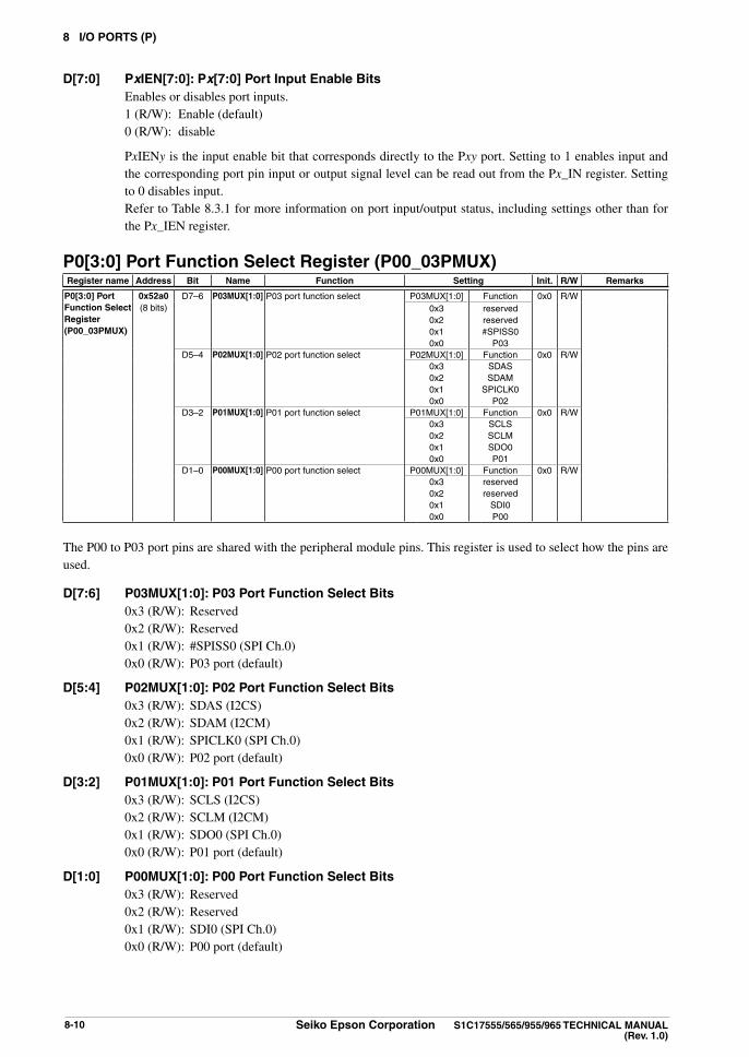
8 i/O PORTS (P)
8-10 Seiko epson Corporation S1C17555/565/955/965 TeChniCal Manual (Rev. 1.0)
D[7:0] Pxien[7:0]: Px[7:0] Port input enable Bits Enables or disables port inputs. 1 (R/W): Enable (default) 0 (R/W): disable
PxIENy is the input enable bit that corresponds directly to the Pxy port. Setting to 1 enables input and the corresponding port pin input or output signal level can be read out from the Px_IN register. Setting to 0 disables input.
Refer to Table 8.3.1 for more information on port input/output status, including settings other than for the Px_IEN register.
P0[3:0] Port Function Select Register (P00_03PMuX)Register name address Bit name Function Setting init. R/W Remarks
P0[3:0] Port Function Select Register(P00_03PMuX)
0x52a0(8 bits)
D7–6 P03MuX[1:0] P03 port function select P03MUX[1:0] Function 0x0 R/W0x30x20x10x0
reservedreserved#SPISS0
P03D5–4 P02MuX[1:0] P02 port function select P02MUX[1:0] Function 0x0 R/W
0x30x20x10x0
SDASSDAM
SPICLK0P02
D3–2 P01MuX[1:0] P01 port function select P01MUX[1:0] Function 0x0 R/W0x30x20x10x0
SCLSSCLMSDO0P01
D1–0 P00MuX[1:0] P00 port function select P00MUX[1:0] Function 0x0 R/W0x30x20x10x0
reservedreserved
SDI0P00
The P00 to P03 port pins are shared with the peripheral module pins. This register is used to select how the pins are used.
D[7:6] P03MuX[1:0]: P03 Port Function Select Bits 0x3 (R/W): Reserved 0x2 (R/W): Reserved 0x1 (R/W): #SPISS0 (SPI Ch.0) 0x0 (R/W): P03 port (default)
D[5:4] P02MuX[1:0]: P02 Port Function Select Bits 0x3 (R/W): SDAS (I2CS) 0x2 (R/W): SDAM (I2CM) 0x1 (R/W): SPICLK0 (SPI Ch.0) 0x0 (R/W): P02 port (default)
D[3:2] P01MuX[1:0]: P01 Port Function Select Bits 0x3 (R/W): SCLS (I2CS) 0x2 (R/W): SCLM (I2CM) 0x1 (R/W): SDO0 (SPI Ch.0) 0x0 (R/W): P01 port (default)
D[1:0] P00MuX[1:0]: P00 Port Function Select Bits 0x3 (R/W): Reserved 0x2 (R/W): Reserved 0x1 (R/W): SDI0 (SPI Ch.0) 0x0 (R/W): P00 port (default)

8 i/O PORTS (P)
S1C17555/565/955/965 TeChniCal Manual Seiko epson Corporation 8-11(Rev. 1.0)
P0[7:4] Port Function Select Register (P04_07PMuX)Register name address Bit name Function Setting init. R/W Remarks
P0[7:4] Port Function Select Register(P04_07PMuX)
0x52a1(8 bits)
D7–6 P07MuX[1:0] P07 port function select P07MUX[1:0] Function 0x0 R/W0x30x20x10x0
reservedSCLSSCLMP07
D5–4 P06MuX[1:0] P06 port function select P06MUX[1:0] Function 0x0 R/W0x30x20x10x0
#BFRFOUTASCLK0
P06D3–2 P05MuX[1:0] P05 port function select P05MUX[1:0] Function 0x0 R/W
0x30x20x10x0
reservedreservedSOUT0
P05D1–0 P04MuX[1:0] P04 port function select P04MUX[1:0] Function 0x0 R/W
0x30x20x10x0
reservedreserved
SIN0P04
The P04 to P07 port pins are shared with the peripheral module pins. This register is used to select how the pins are used.
D[7:6] P07MuX[1:0]: P07 Port Function Select Bits 0x3 (R/W): Reserved 0x2 (R/W): SCLS (I2CS) 0x1 (R/W): SCLM (I2CM) 0x0 (R/W): P07 port (default)
D[5:4] P06MuX[1:0]: P06 Port Function Select Bits 0x3 (R/W): #BFR (I2CS) 0x2 (R/W): FOUTA (CLG) 0x1 (R/W): SCLK0 (UART Ch.0) 0x0 (R/W): P06 port (default)
D[3:2] P05MuX[1:0]: P05 Port Function Select Bits 0x3 (R/W): Reserved 0x2 (R/W): Reserved 0x1 (R/W): SOUT0 (UART Ch.0) 0x0 (R/W): P05 port (default)
D[1:0] P04MuX[1:0]: P04 Port Function Select Bits 0x3 (R/W): Reserved 0x2 (R/W): Reserved 0x1 (R/W): SIN0 (UART Ch.0) 0x0 (R/W): P04 port (default)

8 i/O PORTS (P)
8-12 Seiko epson Corporation S1C17555/565/955/965 TeChniCal Manual (Rev. 1.0)
P1[3:0] Port Function Select Register (P10_13PMuX)Register name address Bit name Function Setting init. R/W Remarks
P1[3:0] Port Function Select Register(P10_13PMuX)
0x52a2(8 bits)
D7–6 P13MuX[1:0] P13 port function select P13MUX[1:0] Function 0x0 R/W0x30x20x10x0
reservedreservedSPICLK1
P13(EXCL1)D5–4 P12MuX[1:0] P12 port function select P12MUX[1:0] Function 0x0 R/W
0x30x20x10x0
reservedreserved
SDO1P12(EXCL0)
D3–2 P11MuX[1:0] P11 port function select P11MUX[1:0] Function 0x0 R/W0x30x20x10x0
reservedTOUTA1/CAPA1
SDI1P11
D1–0 P10MuX[1:0] P10 port function select P10MUX[1:0] Function 0x0 R/W0x30x20x10x0
reservedSDASSDAMP10
The P10 to P13 port pins are shared with the peripheral module pins. This register is used to select how the pins are used.
D[7:6] P13MuX[1:0]: P13 Port Function Select Bits 0x3 (R/W): Reserved 0x2 (R/W): Reserved 0x1 (R/W): SPICLK1 (SPI Ch.1) 0x0 (R/W): P13 port/EXCL1 (T16A2 Ch.1) (default)
To use the P13 pin for EXCL1 input, P1OEN3/P1_OEN register must be set to 0 and P1IEN3/P1_IEN register must be set to 1.
D[5:4] P12MuX[1:0]: P12 Port Function Select Bits 0x3 (R/W): Reserved 0x2 (R/W): Reserved 0x1 (R/W): SDO1 (SPI Ch.1) 0x0 (R/W): P12 port/EXCL0 (T16A2 Ch.0) (default)
To use the P12 pin for EXCL0 input, P1OEN2/P1_OEN register must be set to 0 and P1IEN2/P1_IEN register must be set to 1.
D[3:2] P11MuX[1:0]: P11 Port Function Select Bits 0x3 (R/W): Reserved 0x2 (R/W): TOUTA1 (T16A2 Ch.1 comparator mode)/CAPA1 (T16A2 Ch.1 capture mode) 0x1 (R/W): SDI1 (SPI Ch.1) 0x0 (R/W): P11 port (default)
D[1:0] P10MuX[1:0]: P10 Port Function Select Bits 0x3 (R/W): Reserved 0x2 (R/W): SDAS (I2CS) 0x1 (R/W): SDAM (I2CM) 0x0 (R/W): P10 port (default)
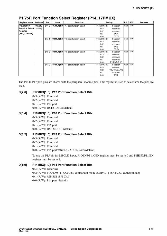
8 i/O PORTS (P)
S1C17555/565/955/965 TeChniCal Manual Seiko epson Corporation 8-13(Rev. 1.0)
P1[7:4] Port Function Select Register (P14_17PMuX)Register name address Bit name Function Setting init. R/W Remarks
P1[7:4] Port Function Select Register(P14_17PMuX)
0x52a3(8 bits)
D7–6 P17MuX[1:0] P17 port function select P17MUX[1:0] Function 0x0 R/W0x30x20x10x0
reservedreserved
P17DST2
D5–4 P16MuX[1:0] P16 port function select P16MUX[1:0] Function 0x0 R/W0x30x20x10x0
reservedreserved
P16DSIO
D3–2 P15MuX[1:0] P15 port function select P15MUX[1:0] Function 0x0 R/W0x30x20x10x0
reservedreservedreserved
P15(MSCLK)D1–0 P14MuX[1:0] P14 port function select P14MUX[1:0] Function 0x0 R/W
0x30x20x10x0
reservedTOUTA0/CAPA0
#SPISS1P14
The P14 to P17 port pins are shared with the peripheral module pins. This register is used to select how the pins are used.
D[7:6] P17MuX[1:0]: P17 Port Function Select Bits 0x3 (R/W): Reserved 0x2 (R/W): Reserved 0x1 (R/W): P17 port 0x0 (R/W): DST2 (DBG) (default)
D[5:4] P16MuX[1:0]: P16 Port Function Select Bits 0x3 (R/W): Reserved 0x2 (R/W): Reserved 0x1 (R/W): P16 port 0x0 (R/W): DSIO (DBG) (default)
D[3:2] P15MuX[1:0]: P15 Port Function Select Bits 0x3 (R/W): Reserved 0x2 (R/W): Reserved 0x1 (R/W): Reserved 0x0 (R/W): P15 port/MSCLK (ADC12SA2) (default)
To use the P15 pin for MSCLK input, P1OEN5/P1_OEN register must be set to 0 and P1IEN5/P1_IEN register must be set to 1.
D[1:0] P14MuX[1:0]: P14 Port Function Select Bits 0x3 (R/W): Reserved 0x2 (R/W): TOUTA0 (T16A2 Ch.0 comparator mode)/CAPA0 (T16A2 Ch.0 capture mode) 0x1 (R/W): #SPISS1 (SPI Ch.1) 0x0 (R/W): P14 port (default)

8 i/O PORTS (P)
8-14 Seiko epson Corporation S1C17555/565/955/965 TeChniCal Manual (Rev. 1.0)
P2[3:0] Port Function Select Register (P20_23PMuX)Register name address Bit name Function Setting init. R/W Remarks
P2[3:0] Port Function Select Register(P20_23PMuX)
0x52a4(8 bits)
D7–6 P23MuX[1:0] P23 port function select P23MUX[1:0] Function 0x0 R/W * S1C17565/965 only0x3
0x20x10x0
reserved SCLK1*SPISS2
P23(EXCL2)D5–4 P22MuX[1:0] P22 port function select P22MUX[1:0] Function 0x0 R/W
0x30x20x10x0
reservedREMI*
SPICLK2P22
D3–2 P21MuX[1:0] P21 port function select P21MUX[1:0] Function 0x0 R/W0x30x20x10x0
reservedFOUTBSDO2P21
D1–0 P20MuX[1:0] P20 port function select P20MUX[1:0] Function 0x0 R/W0x30x20x10x0
reservedTOUTA2/CAPA2
SDI2P20
The P20 to P23 port pins are shared with the peripheral module pins. This register is used to select how the pins are used.
D[7:6] P23MuX[1:0]: P23 Port Function Select Bits 0x3 (R/W): Reserved 0x2 (R/W): SCLK1 (UART Ch.1) [S1C17565/965] 0x1 (R/W): SPISS2 (SPI16) 0x0 (R/W): P23 port/EXCL2 (T16A2 Ch.2) (default)
To use the P23 pin for EXCL2 input, P2OEN3/P2_OEN register must be set to 0 and P2IEN3/P2_IEN register must be set to 1.
D[5:4] P22MuX[1:0]: P22 Port Function Select Bits 0x3 (R/W): Reserved 0x2 (R/W): REMI (REMC) [S1C17565/965] 0x1 (R/W): SPICLK2 (SPI16) 0x0 (R/W): P22 port (default)
D[3:2] P21MuX[1:0]: P21 Port Function Select Bits 0x3 (R/W): Reserved 0x2 (R/W): FOUTB (CLG) 0x1 (R/W): SDO2 (SPI16) 0x0 (R/W): P21 port (default)
D[1:0] P20MuX[1:0]: P20 Port Function Select Bits 0x3 (R/W): Reserved 0x2 (R/W): TOUTA2 (T16A2 Ch.2 comparator mode)/CAPA2 (T16A2 Ch.2 capture mode) 0x1 (R/W): SDI2 (SPI16) 0x0 (R/W): P20 port (default)

8 i/O PORTS (P)
S1C17555/565/955/965 TeChniCal Manual Seiko epson Corporation 8-15(Rev. 1.0)
P2[7:4] Port Function Select Register (P24_27PMuX)Register name address Bit name Function Setting init. R/W Remarks
P2[7:4] Port Function Select Register(P24_27PMuX)
S1C17565/965
0x52a5(8 bits)
D7–6 P27MuX[1:0] P27 port function select P27MUX[1:0] Function 0x0 R/W0x30x20x10x0
reservedSDASSDAMP27
D5–4 P26MuX[1:0] P26 port function select P26MUX[1:0] Function 0x0 R/W0x30x20x10x0
reservedSCLSSCLMP26
D3–2 P25MuX[1:0] P25 port function select P25MUX[1:0] Function 0x0 R/W0x30x20x10x0
reservedREMOSOUT1
P25D1–0 P24MuX[1:0] P24 port function select P24MUX[1:0] Function 0x0 R/W
0x30x20x10x0
reservedTOUTA3/CAPA3
SIN1P24
The P24 to P27 port pins are shared with the peripheral module pins. This register is used to select how the pins are used.
D[7:6] P27MuX[1:0]: P27 Port Function Select Bits (S1C17565/965) 0x3 (R/W): Reserved 0x2 (R/W): SDAS (I2CS) 0x1 (R/W): SDAM (I2CM) 0x0 (R/W): P27 port (default)
D[5:4] P26MuX[1:0]: P26 Port Function Select Bits (S1C17565/965) 0x3 (R/W): Reserved 0x2 (R/W): SCLS (I2CS) 0x1 (R/W): SCLM (I2CM) 0x0 (R/W): P26 port (default)
D[3:2] P25MuX[1:0]: P25 Port Function Select Bits (S1C17565/965) 0x3 (R/W): Reserved 0x2 (R/W): REMO (REMC) 0x1 (R/W): SOUT1 (UART Ch.1) 0x0 (R/W): P25 port (default)
D[1:0] P24MuX[1:0]: P24 Port Function Select Bits (S1C17565/965) 0x3 (R/W): Reserved 0x2 (R/W): TOUTA3 (T16A2 Ch.3 comparator mode)/CAPA3 (T16A2 Ch.3 capture mode) 0x1 (R/W): SIN1 (UART Ch.1) 0x0 (R/W): P24 port (default)

9 16-BiT TiMeRS (T16)
S1C17555/565/955/965 TeChniCal Manual Seiko epson Corporation 9-1(Rev. 1.0)
16-bit Timers (T16)9
T16 Module Overview9.1 The S1C17555/565/955/965 includes three-channel 16-bit timer module (T16).The features of the T16 module are listed below.
• 16-bit presettable down counter with a 16-bit reload data register for setting the preset value
• Generates the SPI and I2C master operating clocks from the counter underflow signals.
• Generates underflow interrupt signals to the interrupt controller (ITC).
• Any desired time intervals and serial transfer rates can be programmed by selecting an appropriate count clock and preset value.
Figure 9.1.1 shows the T16 configuration.
Reload data registerT16_TRx
PRUNDF[3:0]
Underflow
Run/stop control
Inte
rnal
dat
a bu
sCount clock select
Interrupt request
Clock outputs
To ITC
To SPI (from Ch.1)To I2C master (from Ch.2)
PCLK
PRESER Timer reset
Down counterT16_TCx
Control circuit
Count mode select TRMD 16-bit timer Ch.x
Divider(1/1–1/16K)
CLG
1.1 T16 Configuration (1 Channel)Figure 9.
Each channel of the T16 module consists of a 16-bit presettable down counter and a 16-bit reload data register holding the preset value. The timer counts down from the initial value set in the reload data register and outputs an underflow signal when the counter underflows. The underflow signal is used to generate an interrupt and an internal serial interface clock. The underflow cycle can be programmed by selecting the count clock and reload data, en-abling the application program to obtain time intervals and serial transfer rates as required.
note: All three T16 channels have the same functions except for the control register addresses. The de-scription in this chapter applies to all channels. The ‘x’ in the register name refers to the channel number (0 to 2).
Example: T16_CTLx register Ch.0: T16_CTL0 register Ch.1: T16_CTL1 register Ch.2: T16_CTL2 register

9 16-BiT TiMeRS (T16)
9-2 Seiko epson Corporation S1C17555/565/955/965 TeChniCal Manual (Rev. 1.0)
Count Clock9.2 The count clock is generated by dividing the PCLK clock into 1/1 to 1/16K. The division ratio can be selected from the 15 types shown below using DF[3:0]/T16_CLKx register.
2.1 PCLK Division Ratio SelectionTable 9.
DF[3:0] Division ratio DF[3:0] Division ratio
0xf Reserved 0x7 1/1280xe 1/16384 0x6 1/640xd 1/8192 0x5 1/320xc 1/4096 0x4 1/160xb 1/2048 0x3 1/80xa 1/1024 0x2 1/40x9 1/512 0x1 1/20x8 1/256 0x0 1/1
(Default: 0x0)
notes: • The clock generator (CLG) must be configured to supply PCLK to the peripheral modules be-fore running the timer.
• Make sure the counter is halted before setting the count clock.
For detailed information on the CLG control, see the “Clock Generator (CLG)” chapter.
Count Mode9.3 The T16 module features two count modes: repeat mode and one-shot mode. These modes are selected using TRMD/T16_CTLx register.
Repeat mode (TRMD = 0, default) Setting TRMD to 0 sets T16 to repeat mode. In this mode, once the count starts, the timer continues running until stopped by the application program. When
the counter underflows, the timer presets the reload data register value into the counter and continues the count. Thus, the timer periodically outputs an underflow pulse. T16 should be set to this mode to generate periodic in-terrupts at desired intervals or to generate a serial transfer clock.
One-shot mode (TRMD = 1) Setting TRMD to 1 sets T16 to one-shot mode. In this mode, the timer stops automatically as soon as the counter underflows. This means only one interrupt
can be generated after the timer starts. Note that the timer presets the reload data register value to the counter, then stops after an underflow has occurred. T16 should be set to this mode to set a specific wait time.
Reload Data Register and underflow Cycle9.4 The reload data register T16_TRx is used to set the initial value for the down counter.The initial counter value set in the reload data register is preset to the down counter if the timer is reset or the coun-ter underflows. If the timer is started after resetting, it counts down from the reload value (initial value). This means that the reload value and the input clock frequency determine the time elapsed from the point at which the timer starts until the underflow occurs (or between underflows). The time determined is used to obtain the specified wait time, the intervals between periodic interrupts, and the programmable serial interface transfer clock.

9 16-BiT TiMeRS (T16)
S1C17555/565/955/965 TeChniCal Manual Seiko epson Corporation 9-3(Rev. 1.0)
One-shot mode
Counter
Repeat mode
Counter
01n-1n n
Preset by resetting the timer
Preset by resetting the timer
Preset automatically
Underflow
Preset automatically
(n = Reload data)
01n-1n n
Underflow
Timer starts
Timer starts
Preset automatically
01n-1 n
Underflow
4.1 Preset TimingFigure 9.
The underflow cycle can be calculated as follows:
TR + 1 ct_clkUnderflow interval = ———— [s] Underflow cycle = ———— [Hz] ct_clk TR + 1
ct_clk: Count clock frequency [Hz]TR: Reload data (0–65535)
Timer Reset9.5 The timer is reset by writing 1 to PRESER/T16_CTLx register. The reload data is preset and the counter is initial-ized.
Timer Run/STOP Control9.6 Make the following settings before starting the timer.(1) Select the count clock. See Section 9.2.(2) Set the count mode (one-shot or repeat). See Section 9.3.(3) Calculate the initial counter value and set it to the reload data register. See Section 9.4.(4) Reset the timer to preset the counter to the initial value. See Section 9.5.(5) When using timer interrupts, set the interrupt level and enable interrupts for the relevant timer channel. See
Section 9.8.
To start the timer, write 1 to PRUN/T16_CTLx register.The timer starts counting down from the initial value or from the current counter value if no initial value was preset. When the counter underflows, the timer outputs an underflow pulse and presets the counter to the initial value. An interrupt request is sent simultaneously to the interrupt controller (ITC).In one-shot mode, the timer stops counting.In repeat mode, the timer continues counting from the reloaded initial value.
Write 0 to PRUN to stop the timer via the application program. The counter stops counting and retains the current counter value until either the timer is reset or restarted. To restart the count from the initial value, the timer should be reset before writing 1 to PRUN.

9 16-BiT TiMeRS (T16)
9-4 Seiko epson Corporation S1C17555/565/955/965 TeChniCal Manual (Rev. 1.0)
Count clock
PRESER write
PRUN
Counter
Interrupt request
01n-1n n
Count clock
PRESER write
PRUN
Counter
Interrupt request
01n-1n n 01n-1 n n-1
One-shot mode
Repeat mode
Reset by hardwareSet by software
Set by software Reset by software
6.1 Count OperationFigure 9.
T16 Output Signals9.7 The T16 module outputs underflow pulses when the counter underflows. These pulses are used for timer interrupt requests.These pulses are also used to generate the serial transfer clock for the internal serial interface.The clock generated is sent to the internal peripheral module, as shown below.T16 Ch.1 output clock → SPIT16 Ch.2 output clock → I2C master
Use the following equations to calculate the reload data register value for obtaining the desired transfer rate:
ct_clkSPI TR = —————— - 1 bps × 2
ct_clkI2C master TR = —————— - 1 bps × 4
ct_clk: Count clock frequency (Hz)TR: Reload data (0–65535)bps: Transfer rate (bits/s)
T16 interrupts9.8 Each channel of the T16 module outputs an interrupt request to the interrupt controller (ITC) when the counter un-derflows.
underflow interrupt When the counter underflows, the interrupt flag T16IF/T16_INTx register, which is provided for each channel
in the T16 module, is set to 1. At the same time, an interrupt request is sent to the ITC if T16IE/T16_INTx reg-ister has been set to 1 (interrupt enabled). An interrupt is generated if the ITC and S1C17 Core interrupt condi-tions are satisfied.
If T16IE is set to 0 (interrupt disabled, default), no interrupt request will be sent to the ITC. For specific information on interrupt processing, see the “Interrupt Controller (ITC)” chapter.
notes: • The T16 module interrupt flag T16IF must be reset in the interrupt handler routine after a T16 interrupt has occurred to prevent recurring interrupts.
• Reset T16IF before enabling T16 interrupts with T16IE to prevent occurrence of unwanted in-terrupt. T16IF is reset by writing 1.

9 16-BiT TiMeRS (T16)
S1C17555/565/955/965 TeChniCal Manual Seiko epson Corporation 9-5(Rev. 1.0)
Control Register Details9.9 9.1 List of T16 RegistersTable 9.
address Register name Function0x4220 T16_CLK0 T16 Ch.0 Count Clock Select Register Selects a count clock.0x4222 T16_TR0 T16 Ch.0 Reload Data Register Sets reload data.0x4224 T16_TC0 T16 Ch.0 Counter Data Register Counter data0x4226 T16_CTL0 T16 Ch.0 Control Register Sets the timer mode and starts/stops the timer.0x4228 T16_INT0 T16 Ch.0 Interrupt Control Register Controls the interrupt.0x4240 T16_CLK1 T16 Ch.1 Count Clock Select Register Selects a count clock.0x4242 T16_TR1 T16 Ch.1 Reload Data Register Sets reload data.0x4244 T16_TC1 T16 Ch.1 Counter Data Register Counter data0x4246 T16_CTL1 T16 Ch.1 Control Register Sets the timer mode and starts/stops the timer.0x4248 T16_INT1 T16 Ch.1 Interrupt Control Register Controls the interrupt.0x4260 T16_CLK2 T16 Ch.2 Count Clock Select Register Selects a count clock.0x4262 T16_TR2 T16 Ch.2 Reload Data Register Sets reload data.0x4264 T16_TC2 T16 Ch.2 Counter Data Register Counter data0x4266 T16_CTL2 T16 Ch.2 Control Register Sets the timer mode and starts/stops the timer.0x4268 T16_INT2 T16 Ch.2 Interrupt Control Register Controls the interrupt.
The T16 registers are described in detail below.
note: When data is written to the registers, the “Reserved” bits must always be written as 0 and not 1.
T16 Ch.x Count Clock Select Registers (T16_ClKx)Register name address Bit name Function Setting init. R/W Remarks
T16 Ch.x Count Clock Select Register(T16_ClKx)
0x42200x42400x4260(16 bits)
D15–4 – reserved – – – 0 when being read.D3–0 DF[3:0] Count clock division ratio select DF[3:0] Division ratio 0x0 R/W Source clock = PCLK
0xf0xe0xd0xc0xb0xa0x90x80x70x60x50x40x30x20x10x0
reserved1/163841/81921/40961/20481/10241/5121/2561/1281/641/321/161/81/41/21/1
D[15:4] Reserved
D[3:0] DF[3:0]: Count Clock Division Ratio Select Bits Selects a PCLK division ratio to generate the count clock.
9.2 PCLK Division Ratio SelectionTable 9.
DF[3:0] Division ratio DF[3:0] Division ratio
0xf Reserved 0x7 1/1280xe 1/16384 0x6 1/640xd 1/8192 0x5 1/320xc 1/4096 0x4 1/160xb 1/2048 0x3 1/80xa 1/1024 0x2 1/40x9 1/512 0x1 1/20x8 1/256 0x0 1/1
(Default: 0x0)
note: Make sure the counter is halted before setting the count clock.
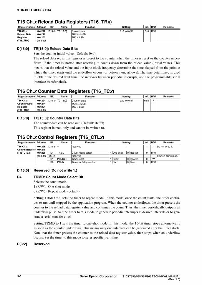
9 16-BiT TiMeRS (T16)
9-6 Seiko epson Corporation S1C17555/565/955/965 TeChniCal Manual (Rev. 1.0)
T16 Ch.x Reload Data Registers (T16_TRx)Register name address Bit name Function Setting init. R/W Remarks
T16 Ch.x Reload Data Register(T16_TRx)
0x42220x42420x4262(16 bits)
D15–0 TR[15:0] Reload dataTR15 = MSBTR0 = LSB
0x0 to 0xffff 0x0 R/W
D[15:0] TR[15:0]: Reload Data Bits Sets the counter initial value. (Default: 0x0) The reload data set in this register is preset to the counter when the timer is reset or the counter under-
flows. If the timer is started after resetting, it counts down from the reload value (initial value). This means that the reload value and the input clock frequency determine the time elapsed from the point at which the timer starts until the underflow occurs (or between underflows). The time determined is used to obtain the desired wait time, the intervals between periodic interrupts, and the programmable serial interface transfer clock.
T16 Ch.x Counter Data Registers (T16_TCx)Register name address Bit name Function Setting init. R/W Remarks
T16 Ch.x Counter Data Register(T16_TCx)
0x42240x42440x4264(16 bits)
D15–0 TC[15:0] Counter dataTC15 = MSBTC0 = LSB
0x0 to 0xffff 0xffff R
D[15:0] TC[15:0]: Counter Data Bits The counter data can be read out. (Default: 0xffff) This register is read-only and cannot be written to.
T16 Ch.x Control Registers (T16_CTlx)Register name address Bit name Function Setting init. R/W Remarks
T16 Ch.x Control Register(T16_CTlx)
0x42260x42460x4266(16 bits)
D15–5 – reserved – – – Do not write 1.
D4 TRMD Count mode select 1 One shot 0 Repeat 0 R/WD3–2 – reserved – – – 0 when being read.
D1 PReSeR Timer reset 1 Reset 0 Ignored 0 WD0 PRun Timer run/stop control 1 Run 0 Stop 0 R/W
D[15:5] Reserved (Do not write 1.)
D4 TRMD: Count Mode Select Bit Selects the count mode. 1 (R/W): One-shot mode 0 (R/W): Repeat mode (default)
Setting TRMD to 0 sets the timer to repeat mode. In this mode, once the count starts, the timer contin-ues to run until stopped by the application program. When the counter underflows, the timer presets the counter to the reload data register value and continues the count. Thus, the timer periodically outputs an underflow pulse. Set the timer to this mode to generate periodic interrupts at desired intervals or to gen-erate a serial transfer clock.
Setting TRMD to 1 sets the timer to one-shot mode. In this mode, the 16-bit timer stops automatically as soon as the counter underflows. This means only one interrupt can be generated after the timer starts. Note that the timer presets the counter to the reload data register value, then stops when an underflow occurs. Set the timer to this mode to set a specific wait time.
D[3:2] Reserved

9 16-BiT TiMeRS (T16)
S1C17555/565/955/965 TeChniCal Manual Seiko epson Corporation 9-7(Rev. 1.0)
D1 PReSeR: Timer Reset Bit Resets the timer. 1 (W): Reset 0 (W): Ignored 0 (R): Always 0 when read (default)
Writing 1 to this bit presets the counter to the reload data value.
D0 PRun: Timer Run/Stop Control Bit Controls the timer RUN/STOP. 1 (R/W): Run 0 (R/W): Stop (default)
The timer starts counting when PRUN is written as 1 and stops when written as 0. When the timer is stopped, the counter data is retained until reset or until the next RUN state.
T16 Ch.x interrupt Control Registers (T16_inTx)Register name address Bit name Function Setting init. R/W Remarks
T16 Ch.x interrupt Control Register(T16_inTx)
0x42280x42480x4268(16 bits)
D15–9 – reserved – – – 0 when being read.D8 T16ie T16 interrupt enable 1 Enable 0 Disable 0 R/W
D7–1 – reserved – – – 0 when being read.D0 T16iF T16 interrupt flag 1 Cause of
interrupt occurred
0 Cause of interrupt not occurred
0 R/W Reset by writing 1.
D[15:9] Reserved
D8 T16ie: T16 interrupt enable Bit Enables or disables interrupts caused by counter underflows for each channel. 1 (R/W): Interrupt enabled 0 (R/W): Interrupt disabled (default)
Setting T16IE to 1 enables T16 interrupt requests to the ITC; setting to 0 disables interrupts.
D[7:1] Reserved
D0 T16iF: T16 interrupt Flag Bit Indicates whether the cause of counter underflow interrupt has occurred or not. 1 (R): Cause of interrupt has occurred 0 (R): No cause of interrupt has occurred (default) 1 (W): Flag is reset 0 (W): Ignored
T16IF is the T16 module interrupt flag that is set to 1 when the counter underflows. T16IF is reset by writing 1.

10 Fine MODe 16-BiT TiMeRS (T16F)
S1C17555/565/955/965 TeChniCal Manual Seiko epson Corporation 10-1(Rev. 1.0)
Fine Mode 16-bit Timers (T16F)10
T16F Module Overview10.1 The S1C17555/565/955/965 includes two-channel fine mode 16-bit timer module (T16F).The features of the T16F module are listed below.
• 16-bit presettable down counter with a 16-bit reload data register for setting the preset value
• Generates underflow interrupt signals to the interrupt controller (ITC).
• Any desired time intervals can be programmed by selecting an appropriate count clock and preset value.
• Fine mode is provided to make fine adjustment of interrupt intervals.
Figure 10.1.1 shows the T16F configuration.
Reload data registerT16F_TRx
PRUNDF[3:0]
Underflow
Run/stop control
Inte
rnal
dat
a bu
sCount clock select
Interrupt requestTo ITC
PRESER Timer reset
Down counterT16F_TCx
Control circuit
Count mode select TRMD
Fine mode setting TFMD[3:0]
Fine mode16-bit timer Ch.x
PCLK Divider(1/1–1/16K)
CLG
1.1 T16F Configuration (1 Channel)Figure 10.
Each channel of the T16F module consists of a 16-bit presettable down counter and a 16-bit reload data register holding the preset value. The timer counts down from the initial value set in the reload data register and outputs an underflow signal when the counter underflows. The underflow signal is used to generate an interrupt. The under-flow cycle can be programmed by selecting the count clock and reload data, enabling the application program to obtain time intervals as required.
note: Both T16F channels have the same functions except for the control register addresses. The de-scription in this chapter applies to both channels. The ‘x’ in the register name refers to the channel number (0 or 1).
Example: T16F_CTLx register Ch.0: T16F_CTL0 register Ch.1: T16F_CTL1 register

10 Fine MODe 16-BiT TiMeRS (T16F)
10-2 Seiko epson Corporation S1C17555/565/955/965 TeChniCal Manual (Rev. 1.0)
Count Clock10.2 The count clock is generated by dividing the PCLK clock into 1/1 to 1/16K. The division ratio can be selected from the 15 types shown below using DF[3:0]/T16F_CLKx register.
2.1 PCLK Division Ratio SelectionTable 10.
DF[3:0] Division ratio DF[3:0] Division ratio
0xf Reserved 0x7 1/1280xe 1/16384 0x6 1/640xd 1/8192 0x5 1/320xc 1/4096 0x4 1/160xb 1/2048 0x3 1/80xa 1/1024 0x2 1/40x9 1/512 0x1 1/20x8 1/256 0x0 1/1
(Default: 0x0)
notes: • The clock generator (CLG) must be configured to supply PCLK to the peripheral modules be-fore running the timer.
• Make sure the counter is halted before setting the count clock.
For detailed information on the CLG control, see the “Clock Generator (CLG)” chapter.
Count Mode10.3 The T16F module features two count modes: repeat mode and one-shot mode. These modes are selected using TRMD/T16F_CTLx register.
Repeat mode (TRMD = 0, default) Setting TRMD to 0 sets T16F to repeat mode. In this mode, once the count starts, the timer continues running until stopped by the application program. When
the counter underflows, the timer presets the reload data register value into the counter and continues the count. Thus, the timer periodically outputs an underflow pulse. T16F should be set to this mode to generate periodic interrupts.
One-shot mode (TRMD = 1) Setting TRMD to 1 sets T16F to one-shot mode. In this mode, the timer stops automatically as soon as the counter underflows. This means only one interrupt
can be generated after the timer starts. Note that the timer presets the reload data register value to the counter, then stops after an underflow has occurred. T16F should be set to this mode to set a specific wait time.
Reload Data Register and underflow Cycle10.4 The reload data register T16F_TRx is used to set the initial value for the down counter.The initial counter value set in the reload data register is preset to the down counter if the timer is reset or the coun-ter underflows. If the timer is started after resetting, it counts down from the reload value (initial value). This means that the reload value and the input clock frequency determine the time elapsed from the point at which the timer starts until the underflow occurs (or between underflows). The time determined is used to obtain the specified wait time and the intervals between periodic interrupts.

10 Fine MODe 16-BiT TiMeRS (T16F)
S1C17555/565/955/965 TeChniCal Manual Seiko epson Corporation 10-3(Rev. 1.0)
One-shot mode
Counter
Repeat mode
Counter
01n-1n n
Preset by resetting the timer
Preset by resetting the timer
Preset automatically
Underflow
Preset automatically
(n = Reload data)
01n-1n n
Underflow
Timer starts
Timer starts
Preset automatically
01n-1 n
Underflow
4.1 Preset TimingFigure 10.
The underflow cycle can be calculated as follows:
TR + 1 ct_clkUnderflow interval = ———— [s] Underflow cycle = ———— [Hz] ct_clk TR + 1
ct_clk: Count clock frequency [Hz]TR: Reload data (0–65535)
Timer Reset10.5 The timer is reset by writing 1 to PRESER/T16F_CTLx register. The reload data is preset and the counter is initial-ized.
Timer Run/STOP Control10.6 Make the following settings before starting the timer.(1) Select the count clock. See Section 10.2.(2) Set the count mode (one-shot or repeat). See Section 10.3.(3) Calculate the initial counter value and set it to the reload data register. See Section 10.4.(4) Reset the timer to preset the counter to the initial value. See Section 10.5.(5) When using timer interrupts, set the interrupt level and enable interrupts for the relevant timer channel. See
Section 10.8.
To start the timer, write 1 to PRUN/T16F_CTLx register.The timer starts counting down from the initial value or from the current counter value if no initial value was preset. When the counter underflows, the timer outputs an underflow pulse and presets the counter to the initial value. An interrupt request is sent simultaneously to the interrupt controller (ITC).In one-shot mode, the timer stops counting.In repeat mode, the timer continues counting from the reloaded initial value.
Write 0 to PRUN to stop the timer via the application program. The counter stops counting and retains the current counter value until either the timer is reset or restarted. To restart the count from the initial value, the timer should be reset before writing 1 to PRUN.

10 Fine MODe 16-BiT TiMeRS (T16F)
10-4 Seiko epson Corporation S1C17555/565/955/965 TeChniCal Manual (Rev. 1.0)
Count clock
PRESER write
PRUN
Counter
Interrupt request
01n-1n n
Count clock
PRESER write
PRUN
Counter
Interrupt request
01n-1n n 01n-1 n n-1
One-shot mode
Repeat mode
Reset by hardwareSet by software
Set by software Reset by software
6.1 Count OperationFigure 10.
Fine Mode10.7 Fine mode provides an interrupt interval fine adjustment function. Fine mode extends the interrupt cycle by delay-ing the underflow pulse from the counter. This delay can be specified with the TFMD[3:0]/T16F_CTLx register. TFMD[3:0] specifies the delay pattern to be inserted into a 16 underflow period. Inserting one delay extends the interrupt cycle by one count clock cycle.
7.1 Delay Patterns Specified by TFMD[3:0]Table 10.
TFMD[3:0]underflow number
1 2 3 4 5 6 7 8 9 10 11 12 13 14 15 16
0x0 – – – – – – – – – – – – – – – –0x1 – – – – – – – – – – – – – – – D0x2 – – – – – – – D – – – – – – – D0x3 – – – – – – – D – – – D – – – D0x4 – – – D – – – D – – – D – – – D0x5 – – – D – – – D – – – D – D – D0x6 – – – D – D – D – – – D – D – D0x7 – – – D – D – D – D – D – D – D0x8 – D – D – D – D – D – D – D – D0x9 – D – D – D – D – D – D – D D D0xa – D – D – D D D – D – D – D D D0xb – D – D – D D D – D D D – D D D0xc – D D D – D D D – D D D – D D D0xd – D D D – D D D – D D D D D D D0xe – D D D D D D D – D D D D D D D0xf – D D D D D D D D D D D D D D D
D: Indicates the insertion of a delay cycle.
Count clock
Underflow signal (not corrected)
Underflow signal (corrected)
Interrupt (not corrected)
Interrupt (corrected)
Delayed
15 16
15 16
1
1
7.1 Delay Cycle Insertion in Fine ModeFigure 10.
At initial reset, TFMD[3:0] is set to 0x0, preventing insertion of delay cycles.

10 Fine MODe 16-BiT TiMeRS (T16F)
S1C17555/565/955/965 TeChniCal Manual Seiko epson Corporation 10-5(Rev. 1.0)
T16F interrupts10.8 Each channel of the T16F module outputs an interrupt request to the interrupt controller (ITC) when the counter underflows.
underflow interrupt When the counter underflows, the interrupt flag T16FIF/T16F_INTx register, which is provided for each chan-
nel in the T16F module, is set to 1. At the same time, an interrupt request is sent to the ITC if T16FIE/T16F_INTx register has been set to 1 (interrupt enabled). An interrupt is generated if the ITC and S1C17 Core inter-rupt conditions are satisfied.
If T16FIE is set to 0 (interrupt disabled, default), no interrupt request will be sent to the ITC. For specific information on interrupt processing, see the “Interrupt Controller (ITC)” chapter.
notes: • The T16F module interrupt flag T16FIF must be reset in the interrupt handler routine after a T16F interrupt has occurred to prevent recurring interrupts.
• Reset T16FIF before enabling T16F interrupts with T16FIE to prevent occurrence of unwanted interrupt. T16FIF is reset by writing 1.
Control Register Details10.9 9.1 List of T16F RegistersTable 10.
address Register name Function0x4200 T16F_CLK0 T16F Ch.0 Count Clock Select Register Selects a count clock.0x4202 T16F_TR0 T16F Ch.0 Reload Data Register Sets reload data.0x4204 T16F_TC0 T16F Ch.0 Counter Data Register Counter data0x4206 T16F_CTL0 T16F Ch.0 Control Register Sets the timer mode and starts/stops the timer.0x4208 T16F_INT0 T16F Ch.0 Interrupt Control Register Controls the interrupt.0x4280 T16F_CLK1 T16F Ch.1 Count Clock Select Register Selects a count clock.0x4282 T16F_TR1 T16F Ch.1 Reload Data Register Sets reload data.0x4284 T16F_TC1 T16F Ch.1 Counter Data Register Counter data0x4286 T16F_CTL1 T16F Ch.1 Control Register Sets the timer mode and starts/stops the timer.0x4288 T16F_INT1 T16F Ch.1 Interrupt Control Register Controls the interrupt.
The T16F registers are described in detail below.
note: When data is written to the registers, the “Reserved” bits must always be written as 0 and not 1.
T16F Ch.x Count Clock Select Registers (T16F_ClKx)Register name address Bit name Function Setting init. R/W Remarks
T16F Ch.x Count Clock Select Register(T16F_ClKx)
0x42000x4280(16 bits)
D15–4 – reserved – – – 0 when being read.D3–0 DF[3:0] Count clock division ratio select DF[3:0] Division ratio 0x0 R/W Source clock = PCLK
0xf0xe0xd0xc0xb0xa0x90x80x70x60x50x40x30x20x10x0
reserved1/163841/81921/40961/20481/10241/5121/2561/1281/641/321/161/81/41/21/1
D[15:4] Reserved
D[3:0] DF[3:0]: Count Clock Division Ratio Select Bits Selects a PCLK division ratio to generate the count clock.

10 Fine MODe 16-BiT TiMeRS (T16F)
10-6 Seiko epson Corporation S1C17555/565/955/965 TeChniCal Manual (Rev. 1.0)
9.2 PCLK Division Ratio SelectionTable 10.
DF[3:0] Division ratio DF[3:0] Division ratio
0xf Reserved 0x7 1/1280xe 1/16384 0x6 1/640xd 1/8192 0x5 1/320xc 1/4096 0x4 1/160xb 1/2048 0x3 1/80xa 1/1024 0x2 1/40x9 1/512 0x1 1/20x8 1/256 0x0 1/1
(Default: 0x0)
note: Make sure the counter is halted before setting the count clock.
T16F Ch.x Reload Data Registers (T16F_TRx)Register name address Bit name Function Setting init. R/W Remarks
T16F Ch.x Reload Data Register(T16F_TRx)
0x42020x4282(16 bits)
D15–0 TR[15:0] Reload dataTR15 = MSBTR0 = LSB
0x0 to 0xffff 0x0 R/W
D[15:0] TR[15:0]: Reload Data Bits Sets the counter initial value. (Default: 0x0) The reload data set in this register is preset to the counter when the timer is reset or the counter under-
flows. If the timer is started after resetting, it counts down from the reload value (initial value). This means that the reload value and the input clock frequency determine the time elapsed from the point at which the timer starts until the underflow occurs (or between underflows). The time determined is used to obtain the desired wait time and the intervals between periodic interrupts.
T16F Ch.x Counter Data Registers (T16F_TCx)Register name address Bit name Function Setting init. R/W Remarks
T16F Ch.x Counter Data Register(T16F_TCx)
0x42040x4284(16 bits)
D15–0 TC[15:0] Counter dataTC15 = MSBTC0 = LSB
0x0 to 0xffff 0xffff R
D[15:0] TC[15:0]: Counter Data Bits The counter data can be read out. (Default: 0xffff) This register is read-only and cannot be written to.
T16F Ch.x Control Registers (T16F_CTlx)Register name address Bit name Function Setting init. R/W Remarks
T16F Ch.x Control Register(T16F_CTlx)
0x42060x4286(16 bits)
D15–12 – reserved – – – 0 when being read.D11–8 TFMD[3:0] Fine mode setup 0x0 to 0xf 0x0 R/W Set a number of times
to insert delay into a 16-underflow period.
D7–5 – reserved – – – 0 when being read.D4 TRMD Count mode select 1 One shot 0 Repeat 0 R/W
D3–2 – reserved – – – 0 when being read.D1 PReSeR Timer reset 1 Reset 0 Ignored 0 WD0 PRun Timer run/stop control 1 Run 0 Stop 0 R/W
D[15:12] Reserved
D[11:8] TFMD[3:0]: Fine Mode Setup Bits Makes fine adjustment of the underflow cycle. (Default: 0x0) TFMD[3:0] specifies the delay pattern to be inserted into a 16 underflow period. Inserting one delay
extends the interrupt cycle by one count clock cycle.
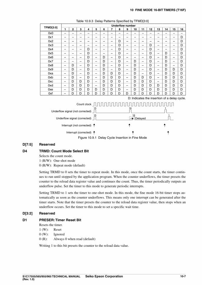
10 Fine MODe 16-BiT TiMeRS (T16F)
S1C17555/565/955/965 TeChniCal Manual Seiko epson Corporation 10-7(Rev. 1.0)
9.3 Delay Patterns Specified by TFMD[3:0]Table 10.
TFMD[3:0]underflow number
1 2 3 4 5 6 7 8 9 10 11 12 13 14 15 160x0 – – – – – – – – – – – – – – – –0x1 – – – – – – – – – – – – – – – D0x2 – – – – – – – D – – – – – – – D0x3 – – – – – – – D – – – D – – – D0x4 – – – D – – – D – – – D – – – D0x5 – – – D – – – D – – – D – D – D0x6 – – – D – D – D – – – D – D – D0x7 – – – D – D – D – D – D – D – D0x8 – D – D – D – D – D – D – D – D0x9 – D – D – D – D – D – D – D D D0xa – D – D – D D D – D – D – D D D0xb – D – D – D D D – D D D – D D D0xc – D D D – D D D – D D D – D D D0xd – D D D – D D D – D D D D D D D0xe – D D D D D D D – D D D D D D D0xf – D D D D D D D D D D D D D D D
D: Indicates the insertion of a delay cycle.
Count clock
Underflow signal (not corrected)
Underflow signal (corrected)
Interrupt (not corrected)
Interrupt (corrected)
Delayed
15 16
15 16
1
1
9.1 Delay Cycle Insertion in Fine ModeFigure 10.
D[7:5] Reserved
D4 TRMD: Count Mode Select Bit Selects the count mode. 1 (R/W): One-shot mode 0 (R/W): Repeat mode (default)
Setting TRMD to 0 sets the timer to repeat mode. In this mode, once the count starts, the timer contin-ues to run until stopped by the application program. When the counter underflows, the timer presets the counter to the reload data register value and continues the count. Thus, the timer periodically outputs an underflow pulse. Set the timer to this mode to generate periodic interrupts.
Setting TRMD to 1 sets the timer to one-shot mode. In this mode, the fine mode 16-bit timer stops au-tomatically as soon as the counter underflows. This means only one interrupt can be generated after the timer starts. Note that the timer presets the counter to the reload data register value, then stops when an underflow occurs. Set the timer to this mode to set a specific wait time.
D[3:2] Reserved
D1 PReSeR: Timer Reset Bit Resets the timer. 1 (W): Reset 0 (W): Ignored 0 (R): Always 0 when read (default)
Writing 1 to this bit presets the counter to the reload data value.

10 Fine MODe 16-BiT TiMeRS (T16F)
10-8 Seiko epson Corporation S1C17555/565/955/965 TeChniCal Manual (Rev. 1.0)
D0 PRun: Timer Run/Stop Control Bit Controls the timer RUN/STOP. 1 (R/W): Run 0 (R/W): Stop (default)
The timer starts counting when PRUN is written as 1 and stops when written as 0. When the timer is stopped, the counter data is retained until reset or until the next RUN state.
T16F Ch.x interrupt Control Registers (T16F_inTx)Register name address Bit name Function Setting init. R/W Remarks
T16F Ch.x interrupt Control Register(T16F_inTx)
0x42080x4288(16 bits)
D15–9 – reserved – – – 0 when being read.D8 T16Fie T16F interrupt enable 1 Enable 0 Disable 0 R/W
D7–1 – reserved – – – 0 when being read.D0 T16FiF T16F interrupt flag 1 Cause of
interrupt occurred
0 Cause of interrupt not occurred
0 R/W Reset by writing 1.
D[15:9] Reserved
D8 T16Fie: T16F interrupt enable Bit Enables or disables interrupts caused by counter underflows for each channel. 1 (R/W): Interrupt enabled 0 (R/W): Interrupt disabled (default)
Setting T16FIE to 1 enables T16F interrupt requests to the ITC; setting to 0 disables interrupts.
D[7:1] Reserved
D0 T16FiF: T16F interrupt Flag Bit Indicates whether the cause of counter underflow interrupt has occurred or not. 1 (R): Cause of interrupt has occurred 0 (R): No cause of interrupt has occurred (default) 1 (W): Flag is reset 0 (W): Ignored
T16FIF is the T16F module interrupt flag that is set to 1 when the counter underflows. T16FIF is reset by writing 1.

11 16-BiT PWM TiMeRS (T16a2)
S1C17555/565/955/965 TeChniCal Manual Seiko epson Corporation 11-1(Rev. 1.0)
16-bit PWM timers (T16A2)11
T16a2 Module Overview11.1 The S1C17555/565/955/965 includes a 16-bit PWM timer (T16A2) module that consists of four channels of coun-ter blocks and comparator/capture blocks. This timer can be used as an interval timer, PWM waveform generator, external event counter and a count capture unit to measure external event periods.The features of T16A2 are listed below.
• Four channels of 16-bit up counter blocks
• Four channels of comparator/capture blocks to which a counter block to be connected is selectable.
• Allows selection of a count clock asynchronously with the CPU clock.
• Supports event counter function using an external clock.
• The comparator compares the counter value with two specified comparison values to generate interrupts and a PWM waveform.
• The capture unit captures counter values using an external trigger signal and generates interrupts.
• A 12-bit A/D converter trigger signal can be output from T16A2 Ch.3.
Figure 11.1.1 shows the T16A2 configuration.
TOUTA3CAPA3
Interrupt request
ADC12SA2 trigger
TOUTA2CAPA2
Interrupt request
TOUTA1CAPA1
Interrupt request
Capture circuit
Comparator circuit
Compare Bbuffer
Compare Abuffer
Comparator circuit
TOUTcontrol circuit
Interruptcontrol circuit
TOUTA0
CAPA0
Interrupt request
Compare B/Capture B registerT16A_CCB0
Compare A/Capture A registerT16A_CCA0
Counter block Ch.0 Comparator/capture block Ch.0
CounterT16A_TC0
IOSC 0
1
2
3
10
OSC3
EXCL0
Divider(1/1–1/32768)
CLKDIV[3:0]/T16A_CLK0
CLKEN/T16A_CLK0
CLKSRC[1:0]/T16A_CLK0
OSC1 Divider(1/1–1/256)
HCM, TRMD, PRESET, PRUN
/T16A_CTL0
MULTIMD/T16A_CLK0
Compare Asignal
Compare Bsignal
MSCLK
EXCL1
Divider(1/1–1/32768)
Gate
Clock controller Ch.0
16-bit PWM timer (T16A2)
Counter block Ch.3 Comparator/capture block Ch.3Clock controller Ch.3
Counter block Ch.1 Comparator/capture block Ch.1Clock controller Ch.1
CCABCNT[1:0]/T16A_CTL3
CBUFEN/T16A_CTL0
CBUFEN/T16A_CTL0
T16A_IFLG0
T16A_CCCTL0
T16A_IEN0
CCABCNT[1:0]/T16A_CTL2
CCABCNT[1:0]/T16A_CTL1
CCABCNT[1:0]/T16A_CTL0
0123
1 0
1 0
0123
0123
0123
10
EXCL2
Counter block Ch.2 Comparator/capture block Ch.2Clock controller Ch.210
S1C17565/965
S1C17565/965
1.1 T16A2 ConfigurationFigure 11.
Clock controller T16A2 includes four channels of clock controllers that generate the count clock for the counters. The clock
source and division ratio can be selected with software.

11 16-BiT PWM TiMeRS (T16a2)
11-2 Seiko epson Corporation S1C17555/565/955/965 TeChniCal Manual (Rev. 1.0)
Counter block The counter block includes a 16-bit up-counter that operates with an IOSC, OSC3 (S1C17565/965 only), or
OSC1 division clock, or the external count clock input from outside the IC. The T16A2 module allows software to run and stop the counter of each channel, and to reset the counter value (cleared to 0) as well as selection of the count clock. The counter can also be reset by the compare B signal output from the comparator/capture block.
Comparator/capture block The comparator/capture block provides a counter comparison function (comparator mode) and a count capture
function (capture mode). When comparator mode is selected via software, the comparator/capture block can be used as a PWM waveform or clock generator. When capture mode is selected, this block can be used as a count capture unit for measuring external event periods/cycles. The comparator circuit generates the compare A and B signals that represent matching between compare A/B register values (set via software) and the counter value, and outputs the signals to the TOUT control circuit and the interrupt control circuit. The TOUT control circuit generates a PWM or other signal from the compare A and B signals and outputs it to the external TOUTAx pin. The T16A2 Ch.3 compare B signal can also be used as a trigger signal for the 12-bit A/D converter. The capture circuit loads the counter value to the capture A register using the CAPAx input signal that represents external events issued as a trigger. The interrupt control circuit outputs an interrupt signal to the interrupt controller (ITC) module according to the interrupt condition that has been set.
Comparator mode and capture mode cannot be used simultaneously in the same channel.
Combination of counter block channel and comparator/capture block channel Generally, a counter block is connected to the comparator/capture block with the same channel number. The
counter block and the comparator/capture block in different channels can also be connected. This allows a counter to use two or more comparator/capture blocks (details are described later).
note: Each channel of the T16A2 module has the same functions except for the control register ad-dresses. The description in this section applies to all channels of the T16A2 module otherwise a channel number is specified. The ‘x’ in the register name refers to the channel number (0 to 3).
Example: T16A_CTLx register Ch.0: T16A_CTL0 register Ch.1: T16A_CTL1 register Ch.2: T16A_CTL2 register Ch.3: T16A_CTL3 register
T16a2 input/Output Pins11.2 Table 11.2.1 lists the input/output pins for the T16A2 module.
2.1 List of T16A2 PinsTable 11.
Pin name i/O Qty Function
EXCL0 (for Ch.0)EXCL1 (for Ch.1)EXCL2 (for Ch.2)MSCLK (for Ch.3)
I 4 External clock input pinsInputs an external clock for the event counter function.The MSCLK input clock for T16A2 Ch.3 is also used in the 12-bit A/D converter if an external clock is selected.
CAPA0 (for Ch.0)CAPA1 (for Ch.1)CAPA2 (for Ch.2)CAPA3 (for Ch.3)*
I 4 Counter-capture trigger signal input pins (effective in capture mode)The specified edge (falling edge, rising edge, or both) of the signal input to the CAPAx pin captures the counter data into the capture A register.
TOUTA0 (for Ch.0)TOUTA1 (for Ch.1)TOUTA2 (for Ch.2)TOUTA3 (for Ch.3)*
O 4 Timer generating signal output pins (effective in comparator mode)Each channel can output the signals generated from the TOUTAx pin.
* Available only for S1C17565/965
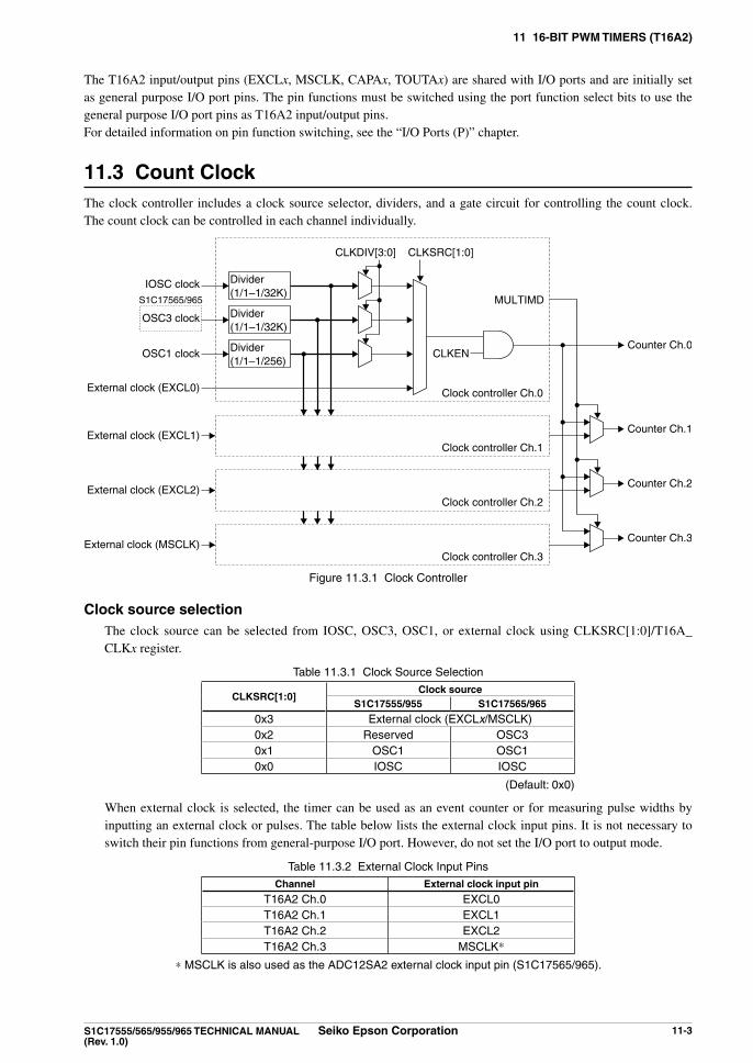
11 16-BiT PWM TiMeRS (T16a2)
S1C17555/565/955/965 TeChniCal Manual Seiko epson Corporation 11-3(Rev. 1.0)
The T16A2 input/output pins (EXCLx, MSCLK, CAPAx, TOUTAx) are shared with I/O ports and are initially set as general purpose I/O port pins. The pin functions must be switched using the port function select bits to use the general purpose I/O port pins as T16A2 input/output pins.For detailed information on pin function switching, see the “I/O Ports (P)” chapter.
Count Clock11.3 The clock controller includes a clock source selector, dividers, and a gate circuit for controlling the count clock. The count clock can be controlled in each channel individually.
OSC1 clock
External clock (EXCL0)
OSC3 clock
CLKSRC[1:0]
MULTIMD
CLKDIV[3:0]
Counter Ch.0CLKEN
Divider(1/1–1/32K)
Divider(1/1–1/256)
Clock controller Ch.0
External clock (EXCL1)Counter Ch.1
IOSC clock Divider(1/1–1/32K)
Clock controller Ch.1
External clock (EXCL2)Counter Ch.2
Clock controller Ch.2
External clock (MSCLK)Counter Ch.3
Clock controller Ch.3
S1C17565/965
3.1 Clock Controller Figure 11.
Clock source selection The clock source can be selected from IOSC, OSC3, OSC1, or external clock using CLKSRC[1:0]/T16A_
CLKx register.
3.1 Clock Source SelectionTable 11.
ClKSRC[1:0]Clock source
S1C17555/955 S1C17565/965
0x3 External clock (EXCLx/MSCLK)0x2 Reserved OSC30x1 OSC1 OSC10x0 IOSC IOSC
(Default: 0x0)
When external clock is selected, the timer can be used as an event counter or for measuring pulse widths by inputting an external clock or pulses. The table below lists the external clock input pins. It is not necessary to switch their pin functions from general-purpose I/O port. However, do not set the I/O port to output mode.
3.2 External Clock Input Pins Table 11.
Channel external clock input pin
T16A2 Ch.0 EXCL0T16A2 Ch.1 EXCL1T16A2 Ch.2 EXCL2T16A2 Ch.3 MSCLK*
* MSCLK is also used as the ADC12SA2 external clock input pin (S1C17565/965).
11 16-BiT PWM TiMeRS (T16a2)
11-4 Seiko epson Corporation S1C17555/565/955/965 TeChniCal Manual (Rev. 1.0)
internal clock division ratio selection When an internal clock (IOSC, OSC3, or OSC1) is selected, use CLKDIV[3:0]/T16A_CLKx register to select
the division ratio.
3.3 Internal Clock Division Ratio SelectionTable 11.
ClKDiV[3:0]Division ratio
Clock source = iOSC or OSC3 Clock source = OSC1
0xf 1/32768 Reserved0xe 1/16384 Reserved0xd 1/8192 Reserved0xc 1/4096 Reserved0xb 1/2048 Reserved0xa 1/1024 Reserved0x9 1/512 Reserved0x8 1/2560x7 1/1280x6 1/640x5 1/320x4 1/160x3 1/80x2 1/40x1 1/20x0 1/1
(Default: 0x0)
Clock enable Clock supply to the counter is controlled using CLKEN/T16A_CLKx register. The CLKEN default setting is
0, which disables the clock supply. Setting CLKEN to 1 sends the clock generated as above to the counter. If T16A2 is not required, disable the clock supply to reduce current consumption.
Multi-comparator/capture mode The T16A2 module allows a counter channel to be connected to multiple comparator/capture channels (multi-
comparator/capture mode). In this case, all channels must be clocked with the Ch.0 clock. Use MULTIMD/T16A_CLK0 register to supply the Ch.0 clock to all channels. When using T16A2 in multi-comparator/capture mode, set MULTIMD to 1. When connecting the counter and comparator/capture block in the same channel (normal channel mode), set MULTIMD to 0 (default).
note: Make sure the T16A2 count is stopped before setting the count clock.
T16a2 Operating Modes11.4 The T16A2 module provides some operating modes to support various usages. This section describes the functions of each operating mode and how to enter the mode.
Comparator Mode and Capture Mode11.4.1
The comparator/capture block includes two registers, T16A_CCAx and T16A_CCBx. The T16A_CCAx register can be set to comparator mode or capture mode using CCAMD/T16A_CCCTLx register. When CCAMD is set to 0, comparator mode is selected; when it is set to 1, capture mode is selected.The T16A_CCBx register supports comparator mode only.
Comparator mode (CCaMD = 0, default) * Supported by both T16A_CCAx and T16A_CCBx
The comparator mode compares the counter value and the comparison value set via software. It generates an interrupt and toggles the timer output signal level when the values are matched. The T16A_CCAx and T16A_CCBx registers function as the compare A and compare B registers that are used for loading compare values in this mode.

11 16-BiT PWM TiMeRS (T16a2)
S1C17555/565/955/965 TeChniCal Manual Seiko epson Corporation 11-5(Rev. 1.0)
When the counter reaches the value set in the compare A register during counting, the comparator asserts the compare A signal. At the same time the compare A interrupt flag is set and the interrupt signal of the timer channel is output to the ITC if the interrupt has been enabled.
When the counter reaches the value set in the compare B register, the comparator asserts the compare B signal. At the same time the compare B interrupt flag is set and the interrupt signal of the timer channel is output to the ITC if the interrupt is enabled. Furthermore, the counter is reset to 0.
The compare A period (time from start of counting to occurrence of a compare A interrupt) and the compare B period (time from start of counting to occurrence of a compare B interrupt) can be calculated as follows:
Compare A period = (CCA + 1) / ct_clk [second] Compare B period = (CCB + 1) / ct_clk [second]
CCA: Compare A register value set (0 to 65535) CCB: Compare B register value set (0 to 65535) ct_clk: Count clock frequency [Hz]
The compare A and compare B signals are also used to generate a timer output waveform (TOUT). See Section 11.6, “Timer Output Control,” for more information. To generate PWM waveform, T16A2 must be set to com-parator mode.
The compare B signal of T16A2 Ch.3 is also used as a conversion trigger signal for the 12-bit A/D converter.
Compare buffers The compare buffer is used to synchronize the comparison data update timings and the counter operation.
Setting CBUFEN/T16A_CTLx register to 1 enables the compare buffer. The compare A and B signals will be generated by comparing the counter values with the compare A and B buffer values instead of the com-pare A and B register values. The compare A and B register values written via software are loaded to the compare A and B buffers when the compare B signal is generated.
Capture mode (CCaMD = 1) * Supported by T16A_CCAx only
The capture mode captures the counter value when an external event such as a key entry occurs (at the specified edge of the external input signal). In this mode, the T16A_CCAx register functions as the capture A register.
The table below lists the input pins of the external trigger signals used for capturing counter values. The pin function of the corresponding ports must be switched for trigger input in advance. See the “I/O Ports (P)” chap-ter for switching the pin function.
4.1.1 List of Counter Capture Trigger Signal Input PinsTable 11.
Channel Capture a trigger input pins
T16A2 Ch.0 CAPA0T16A2 Ch.1 CAPA1T16A2 Ch.2 CAPA2T16A2 Ch.3 CAPA3
The trigger edge of the signal can be selected using the CAPATRG[1:0]/T16A_CCCTLx register .
4.1.2 Capture Trigger Edge SelectionTable 11.
CaPaTRG[1:0] Trigger edge
0x3 Falling edge and rising edge 0x2 Falling edge 0x1 Rising edge 0x0 Not triggered
(Default: 0x0)
When a specified trigger edge is input during counting, the current counter value is loaded to the capture A register. At the same time the capture A interrupt flag is set and the interrupt signal of the timer channel is out-put to the ITC if the interrupt has been enabled. This interrupt can be used to read the captured data from the T16A_CCAx register. For example, external event cycles and pulse widths can be measured from the difference between two captured counter values read.
If the captured data is overwritten by the next trigger when the capture A interrupt flag has already been set, the overwrite interrupt flag will be set. This interrupt can be used to execute an overwrite error handling. To avoid occurrence of unnecessary overwrite interrupt, the capture A interrupt flag must be reset after the captured data has been read from the T16A_CCAx register.
11 16-BiT PWM TiMeRS (T16a2)
11-6 Seiko epson Corporation S1C17555/565/955/965 TeChniCal Manual (Rev. 1.0)
notes: • The correct captured data may not be obtained if the captured data is read at the same time the next value is being captured. Read the capture register twice to check if the read data is correct as necessary.
• To capture counter data properly, both the High and Low period of the CAPAx trigger signal must be longer than the source clock cycle time.
The setting of CAPATRG[1:0] is ineffective in comparator mode. No counter capturing operation will be per-formed even if a trigger edge is specified.
The capture mode cannot generate/output the TOUT signal as no compare signal is generated.
Repeat Mode and One-Shot Mode11.4.2
Each counter features two count modes: repeat mode and one-shot mode. The count mode is selected using TRMD /T16A_CTLx register.
Repeat mode (TRMD = 0, default) Setting TRMD to 0 sets the corresponding counter to repeat mode. In this mode, once the count starts, the counter continues running until stopped by the application program. The
counter continues the count even if the counter returns to 0 due to a counter overflow. The counter should be set to this mode to generate periodic interrupts at desired intervals or to generate a timer output waveform.
One-shot mode (TRMD = 1) Setting TRMD to 1 sets the corresponding counter to one-shot mode. In this mode, the counter stops automatically as soon as the compare B signal is generated. The counter should
be set to this mode to set a specific wait time or for pulse width measurement.
normal Channel Mode and Multi-Comparator/Capture Mode11.4.3
One channel of the T16A2 module basically consists of a counter block and a comparator/capture block. The T16A2 module also allows the application to use expanded comparator/capture function by connecting two or more comparator/capture blocks to one counter block. To support this expansion, two operating modes are provided: normal channel mode and multi-comparator/capture mode. This operating mode can be selected using MULTIMD/T16_CLK0 register.
normal channel mode (MulTiMD = 0, default) Set the T16A2 module to this mode when using it as four channels of different timers by connecting a counter
block with the comparator/capture block of the same channel. In this mode, the counters can use different count clocks.
Each timer channel provides CCABCNT[1:0]/T16A_CTLx register to select a counter channel to be connected to the comparator/capture block.
4.3.1 Counter Selection Table 11.
CCaBCnT[1:0] Counter channel
0x3 Ch.3 (Counter 3)0x2 Ch.2 (Counter 2)0x1 Ch.1 (Counter 1)0x0 Ch.0 (Counter 0)
(Default: 0x0)
When using the T16A2 module in normal channel mode, be sure to connect the counter block to the compara-tor/capture block in the same channel.

11 16-BiT PWM TiMeRS (T16a2)
S1C17555/565/955/965 TeChniCal Manual Seiko epson Corporation 11-7(Rev. 1.0)
Counter block Ch.1 Comparator/capture block Ch.1Clock controller Ch.1
Counter block Ch.0 Comparator/capture block Ch.0Clock controller Ch.0
Counter block Ch.2 Comparator/capture block Ch.2Clock controller Ch.2
Counter block Ch.3 Comparator/capture block Ch.3Clock controller Ch.3
T16A2
Interruptrequest
Interruptrequest
Interruptrequest
Interruptrequest
∗ Available only in S1C17565/965
TOUTA3CAPA3
TOUTA2CAPA2
TOUTA1CAPA1
TOUTA0CAPA0
IOSCOSC3*OSC1EXCL1
IOSCOSC3*OSC1EXCL0
IOSCOSC3*OSC1EXCL2
IOSCOSC3*OSC1MSCLK
4.3.1 Timer Configuration in Normal Channel Mode (two comparators/one capture unit × four channels) Figure 11.
note: Do not connect a counter block to a comparator/capture block in a different channel in normal channel mode (MULTIMD = 0), as normal operation cannot be guaranteed.
Multi-comparator/capture mode (MulTiMD = 1) In order to set three or more comparison values for one counter or to capture the contents of one counter using
two or more trigger signals, two or more comparator/capture blocks can be connected to one counter. Multi-comparator/capture mode is provided for this purpose. In this mode, any counter block can be combined with the comparator/capture blocks using CCABCNT[1:0] described above. Note, however, that the count clock is fixed at one type for counter Ch.0, regardless of the counter to be used. The clock settings for Ch.1 to Ch.3 are ineffective.
Counter block Ch.1 Comparator/capture block Ch.1Clock controller Ch.1
Counter block Ch.0 Comparator/capture block Ch.0Clock controller Ch.0
Counter block Ch.2 Comparator/capture block Ch.2Clock controller Ch.2
Counter block Ch.3 Comparator/capture block Ch.3Clock controller Ch.3
T16A2
Interruptrequest
Interruptrequest
Interruptrequest
Interruptrequest
TOUTA3CAPA3
TOUTA2CAPA2
TOUTA1CAPA1
TOUTA0CAPA0
∗ Available only in S1C17565/965
IOSCOSC3*OSC1EXCL1
IOSCOSC3*OSC1EXCL0
IOSCOSC3*OSC1EXCL2
IOSCOSC3*OSC1MSCLK
(1) Configuration Example 1 (four comparators/two capture units × two channels)
Counter block Ch.1 Comparator/capture block Ch.1Clock controller Ch.1
Counter block Ch.0 Comparator/capture block Ch.0Clock controller Ch.0
T16A2
Counter block Ch.2 Comparator/capture block Ch.2Clock controller Ch.2
Counter block Ch.3 Comparator/capture block Ch.3Clock controller Ch.3
Interruptrequest
Interruptrequest
Interruptrequest
Interruptrequest
TOUTA3CAPA3
TOUTA2CAPA2
TOUTA1CAPA1
TOUTA0CAPA0
∗ Available only in S1C17565/965
IOSCOSC3*OSC1EXCL1
IOSCOSC3*OSC1EXCL0
IOSCOSC3*OSC1EXCL2
IOSCOSC3*OSC1MSCLK
(2) Configuration Example 2 (eight comparators/four capture units × one channel)
4.3.2 Timer Configuration Example in Multi-Comparator/Capture ModeFigure 11.

11 16-BiT PWM TiMeRS (T16a2)
11-8 Seiko epson Corporation S1C17555/565/955/965 TeChniCal Manual (Rev. 1.0)
normal Clock Mode and half Clock Mode11.4.4
T16A2 supports half clock mode to control the duty ratio of the PWM output waveform with high accuracy. In half clock mode, T16A2 uses the dual-edge counter, which counts at the rising and falling edges of the count clock, to compare with the compare A register. This makes it possible to control the duty ratio with double accuracy as compared to normal clock mode.Use HCM/T16A_CTLx register to select half clock mode.
normal clock mode (hCM = 0, default) In normal clock mode, T16A2 generates a compare A signal when the T16A_TCx register value matches the
T16A_CCAx register.
half clock mode (hCM = 1) In half clock mode, T16A2 generates a compare A signal when the dual-edge counter value matches the T16A_
CCAx register.
notes: • T16A2 must be placed into comparator mode to set half clock mode, as it is effective only when PWM waveform is generated.
Be sure to set T16A2 to normal clock mode (HCM = 0) under a condition shown below. (1) When T16A2 is placed into capture mode (2) When TOUTAMD[1:0]/T16A_CCCTLx register is set to 0x2 or 0x3
• The dual-edge counter value cannot be read.
• Do not use the compare A interrupt in half clock mode.
• In half clock mode, the T16A_CCBx register setting value must be less than [T16A_CCAx set-ting value / 2 + 0x8000].
Counter Control 11.5
Counter Reset11.5.1
To reset the counter to 0, write 1 to PRESET/T16A_CTLx register while the count clock is being supplied to the channel. PRESET retains 1 during the reset period and reverts to 0 after the resetting has completed. Normally, the counter should be reset by writing 1 to this bit before starting the count. The counter is reset by the hardware if the counter reaches the compare B register value after the count starts.
Counter Run/STOP Control11.5.2
Make the following settings before starting the count operation.(1) Switch the input/output pin functions to be used for T16A. Refer to the “I/O Port (P)” chapter.(2) Select operating modes. See Section 11.4.(3) Select the clock source. See Section 11.3.(4) Configure the timer outputs (TOUT). See Section 11.6.(5) If using interrupts, set the interrupt level and enable the T16A2 interrupts. See Section 11.7.(6) Reset the counter to 0. See Section 11.5.1.(7) Set comparison data (in comparator mode). See Section 11.4.1.
Each timer channel provides PRUN/T16A_CTLx register to control the counter operation.The counter starts counting when 1 is written to PRUN. Writing 0 to PRUN disables clock input and stops the count.This control does not affect the counter data. The counter data is retained even when the count is halted, allowing resumption of the count from that data.

11 16-BiT PWM TiMeRS (T16a2)
S1C17555/565/955/965 TeChniCal Manual Seiko epson Corporation 11-9(Rev. 1.0)
Reading Counter Values11.5.3
The counter value can be read from T16ATC[15:0]/T16A_TCx register even if the counter is running. However, the counter value should be read at once using a 16-bit transfer instruction. If data is read twice using an 8-bit transfer instruction, the correct value may not be obtained due to occurrence of count up between readings.
Timing Charts11.5.4
Comparator mode
Compare Ainterrupt
Reset andcompare B
interrupt
Compare Ainterrupt
Reset andcompare B
interrupt
PRUN
PRESET
T16A_CCAx
T16A_CCBx
Count clock
T16A_TCx
Reset
0x2
0 1 2 3 4 5 0 1 2 3 4 5 0 1
0x5
5.4.1 Operation Timing in Comparator ModeFigure 11.
Capture mode
PRUN
PRESET
CAPAx
Count clock
T16A_TCx
T16A_CCAx
(when CAPATRG[1:0] = 0x3)
Reset Capture Ainterrupt
Capture Ainterrupt
(and capture A overwriteinterrupt if CAPAIF = 1)
0 1 2 3 4 5 6 7 8 9 10 11 12 13
5 10
5.4.2 Operation Timing in Capture ModeFigure 11.
Timer Output Control11.6 The timer that has been set in comparator mode can generate TOUT signals using the compare A and compare B signals and can output it to external devices. Each timer channel provides one TOUT output, thus the T16A2 mod-ule can output up to four TOUT signals.Figure 11.6.1 shows the TOUT output circuit (one timer channel).
TOUTAxoutput control
Compare A signalCompare B signal
TOUTAMD[1:0]TOUTAINV
TOUTAx
Comparator/capture block Ch.x
6.1 TOUT Output Circuit Figure 11.

11 16-BiT PWM TiMeRS (T16a2)
11-10 Seiko epson Corporation S1C17555/565/955/965 TeChniCal Manual (Rev. 1.0)
TOuT output pins Table 11.6.1 lists correspondence between the TOUT pins and the timer channels. The pin function of the cor-
responding ports must be switched for TOUT output in advance. See the “I/O Ports (P)” chapter for switching the pin function.
6.1 List of TOUT Output PinsTable 11.
Channel TOuT output pin
T16A2 Ch.0 TOUTA0T16A2 Ch.1 TOUTA1T16A2 Ch.2 TOUTA2T16A2 Ch.3 TOUTA3
TOuT generation mode TOUTAMD[1:0]/T16A_CCCTLx register is used to set how the TOUT signal is changed by the compare A and
compare B signals.
6.2 TOUT Generation ModeTable 11.
TOuTaMD[1:0] When compare a occurs When compare B occurs
0x3 No change Toggle0x2 Toggle No change0x1 Rise Fall0x0 Disable output
(Default: 0x0)
TOUTAMD[1:0] is also used to turn the TOUT outputs On and Off.
TOuT signal polarity selection By default, an active High output signal is generated. This logic can be inverted using TOUTAINV/T16A_
CCCTLx register. Writing 1 to TOUTAINV sets the timer to generate an active Low TOUT signal.
Resetting the counter sets the TOUT signal to the inactive level.
Figure 11.6.2 illustrates the TOUT output waveform.
Count clock
PRESET
PRUN
Counter value
Compare A signal
Compare B signal
TOUTA output
(TOUTAMD[1:0] = 0x0, TOUTAINV = 0)
(TOUTAMD[1:0] = 0x0, TOUTAINV = 1)
(TOUTAMD[1:0] = 0x1, TOUTAINV = 0)
(TOUTAMD[1:0] = 0x1, TOUTAINV = 1)
(TOUTAMD[1:0] = 0x2, TOUTAINV = 0)
(TOUTAMD[1:0] = 0x2, TOUTAINV = 1)
(TOUTAMD[1:0] = 0x3, TOUTAINV = 0)
(TOUTAMD[1:0] = 0x3, TOUTAINV = 1)
(When T16A_CCAx = 3, T16A_CCBx = 5)
1 2 3 4 5 00 1 2 3 4 5 0 1 2 3 4 5 0 1
6.2 TOUT Output WaveformFigure 11.

11 16-BiT PWM TiMeRS (T16a2)
S1C17555/565/955/965 TeChniCal Manual Seiko epson Corporation 11-11(Rev. 1.0)
PWM waveform output timings
normal clock mode (hCM = 0)
Count clock
T16A_TCx
TOUTAx
T16A_CCAx
(When TOUTAMD[1:0] = 0x1 and TOUTAINV = 0)
n 0
0
1 2 n-1 n 0 1
1 2 n-2 n-1 (n = T16A_CCBx)
Count clock
T16A_TCx
TOUTAx
Example: HCM = 0, T16A_CCAx = 1, and T16A_CCBx = 5(When TOUTAMD[1:0] = 0x1 and TOUTAINV = 0)
5 0 1 2 4 5 0 13
6.3 PWM Waveform Output Timings in Normal Clock ModeFigure 11.
half clock mode (hCM = 1)
Count clock
T16A_TCx
Dual-edge counter
TOUTAx
T16A_CCAx
(When TOUTAMD[1:0] = 0x1 and TOUTAINV = 0)
n
2n
0
– 0
0
1 2 3 4 2n-3 2n-2 2n-1 2n – 0 1
1 2 n-1 n 0 1
1 2 3 4 2n-4 2n-3 2n-2 2n-1 (n = T16A_CCBx)
Count clock
T16A_TCx
Dual-edge counter
TOUTAx
Example: HCM = 1, T16A_CCAx = 1, and T16A_CCBx = 5(When TOUTAMD[1:0] = 0x1 and TOUTAINV = 0)
5
10
0
– 0 1 2 3 4 7 8 9 10 – 0 1
1 2 4 5 0 1
5 6
3
6.4 PWM Waveform Output Timings in Half Clock ModeFigure 11.
T16a2 interrupts11.7 The T16A2 module can generate the following four kinds of interrupts:• Compare A interrupt (in comparator mode)• Compare B interrupt (in comparator mode)• Capture A interrupt (in capture mode) • Capture A overwrite interrupt (in capture mode)
Each timer channel outputs a single interrupt signal shared by the above interrupt causes to the interrupt controller (ITC). Read the interrupt flags in the T16A2 module to identify the interrupt cause that has been occurred.
interrupts in comparator mode
Compare a interrupt This interrupt request is generated when the counter matches the compare A register value during counting
in comparator mode. It sets the interrupt flag CAIF/T16A_IFLGx register in the T16A2 module to 1. To use this interrupt, set CAIE/T16A_IENx register to 1. If CAIE is set to 0 (default), interrupt requests for
this cause is not sent to the ITC.
11 16-BiT PWM TiMeRS (T16a2)
11-12 Seiko epson Corporation S1C17555/565/955/965 TeChniCal Manual (Rev. 1.0)
Compare B interrupt This interrupt request is generated when the counter matches the compare B register value during counting
in comparator mode. It sets the interrupt flag CBIF/T16A_IFLGx register in the T16A2 module to 1. To use this interrupt, set CBIE/T16A_IENx register to 1. If CBIE is set to 0 (default), interrupt requests for
this cause is not sent to the ITC.
interrupts in capture mode
Capture a interrupt This interrupt request is generated when the counter value is captured in the capture A register by an exter-
nal trigger during counting in capture mode. It sets the interrupt flag CAPAIF/T16A_IFLGx register in the T16A2 module to 1.
To use this interrupt, set CAPAIE/T16A_IENx register to 1. If CAPAIE is set to 0 (default), interrupt re-quests for this cause is not sent to the ITC.
Capture a overwrite interrupt This interrupt request is generated if the capture A register is overwritten by a new external trigger when
the capture A interrupt flag CAPAIF has been set (a counter value has already been loaded to the capture A register). It sets the interrupt flag CAPAOWIF/T16A_IFLGx register in the T16A2 module to 1.
To use this interrupt, set CAPAOWIE/T16A_IENx register to 1. If CAPAOWIE is set to 0 (default), interrupt requests for this cause is not sent to the ITC.
CAPAOWIF will be set if the capture A register is overwritten when CAPAIF has been set regardless of whether the capture A register has been read or not. Therefore, be sure to reset CAPAIF immediately after the capture A register is read.
If the interrupt flag is set to 1 when the interrupt has been enabled, the T16A2 module outputs an interrupt request to the ITC. An interrupt is generated if the ITC and S1C17 core interrupt conditions are satisfied.For more information on interrupt control registers and the operation when an interrupt occurs, see the “Interrupt Controller (ITC)” chapter.
notes: • Reset the interrupt flag before enabling interrupts with the interrupt enable bit to prevent oc-currence of unwanted interrupt. The interrupt flag is reset by writing 1.
• After an interrupt occurs, the interrupt flag in the T16A2 module must be reset in the interrupt handler routine.
Control Register Details11.8 8.1 List of T16A2 RegistersTable 11.
address Register name Function0x5068 T16A_CLK0 T16A2 Clock Control Register Ch.0 Controls the T16A2 Ch.0 clock.0x5069 T16A_CLK1 T16A2 Clock Control Register Ch.1 Controls the T16A2 Ch.1 clock.0x506a T16A_CLK2 T16A2 Clock Control Register Ch.2 Controls the T16A2 Ch.2 clock.0x506b T16A_CLK3 T16A2 Clock Control Register Ch.3 Controls the T16A2 Ch.3 clock.0x5400 T16A_CTL0 T16A2 Counter Ch.0 Control Register Controls the counter.0x5402 T16A_TC0 T16A2 Counter Ch.0 Data Register Counter data0x5404 T16A_CCCTL0 T16A2 Comparator/Capture Ch.0 Control Register Controls the comparator/capture block and TOUT. 0x5406 T16A_CCA0 T16A2 Compare/Capture Ch.0 A Data Register Compare A/capture A data0x5408 T16A_CCB0 T16A2 Compare/Capture Ch.0 B Data Register Compare B data0x540a T16A_IEN0 T16A2 Compare/Capture Ch.0 Interrupt Enable Register Enables/disables interrupts.0x540c T16A_IFLG0 T16A2 Compare/Capture Ch.0 Interrupt Flag Register Displays/sets interrupt occurrence status.0x5420 T16A_CTL1 T16A2 Counter Ch.1 Control Register Controls the counter.0x5422 T16A_TC1 T16A2 Counter Ch.1 Data Register Counter data0x5424 T16A_CCCTL1 T16A2 Comparator/Capture Ch.1 Control Register Controls the comparator/capture block and TOUT. 0x5426 T16A_CCA1 T16A2 Compare/Capture Ch.1 A Data Register Compare A/capture A data0x5428 T16A_CCB1 T16A2 Compare/Capture Ch.1 B Data Register Compare B data0x542a T16A_IEN1 T16A2 Compare/Capture Ch.1 Interrupt Enable Register Enables/disables interrupts.0x542c T16A_IFLG1 T16A2 Compare/Capture Ch.1 Interrupt Flag Register Displays/sets interrupt occurrence status.0x5440 T16A_CTL2 T16A2 Counter Ch.2 Control Register Controls the counter.0x5442 T16A_TC2 T16A2 Counter Ch.2 Data Register Counter data0x5444 T16A_CCCTL2 T16A2 Comparator/Capture Ch.2 Control Register Controls the comparator/capture block and TOUT.

11 16-BiT PWM TiMeRS (T16a2)
S1C17555/565/955/965 TeChniCal Manual Seiko epson Corporation 11-13(Rev. 1.0)
address Register name Function0x5446 T16A_CCA2 T16A2 Compare/Capture Ch.2 A Data Register Compare A/capture A data0x5448 T16A_CCB2 T16A2 Compare/Capture Ch.2 B Data Register Compare B data0x544a T16A_IEN2 T16A2 Compare/Capture Ch.2 Interrupt Enable Register Enables/disables interrupts.0x544c T16A_IFLG2 T16A2 Compare/Capture Ch.2 Interrupt Flag Register Displays/sets interrupt occurrence status.0x5460 T16A_CTL3 T16A2 Counter Ch.3 Control Register Controls the counter.0x5462 T16A_TC3 T16A2 Counter Ch.3 Data Register Counter data0x5464 T16A_CCCTL3 T16A2 Comparator/Capture Ch.3 Control Register Controls the comparator/capture block and TOUT. 0x5466 T16A_CCA3 T16A2 Compare/Capture Ch.3 A Data Register Compare A/capture A data0x5468 T16A_CCB3 T16A2 Compare/Capture Ch.3 B Data Register Compare B data0x546a T16A_IEN3 T16A2 Compare/Capture Ch.3 Interrupt Enable Register Enables/disables interrupts.0x546c T16A_IFLG3 T16A2 Compare/Capture Ch.3 Interrupt Flag Register Displays/sets interrupt occurrence status.
The T16A2 registers are described in detail below.
note: When data is written to the registers, the “Reserved” bits must always be written as 0 and not 1.
T16a2 Clock Control Register Ch.x (T16a_ClKx)Register name address Bit name Function Setting init. R/W Remarks
T16a2 Clock Control Register Ch.x(T16a_ClKx)
0x50680x50690x506a0x506b(8 bits)
D7–4 ClKDiV[3:0]
Clock division ratio selectCLKDIV[3:0]
Division ratio 0x0 R/WOSC3 or
IOSCOSC1
0xf0xe0xd0xc0xb0xa0x90x80x70x60x50x40x30x20x10x0
1/327681/163841/81921/40961/20481/10241/5121/2561/1281/641/321/161/81/41/21/1
–––––––
1/2561/1281/641/321/161/81/41/21/1
D3–2 ClKSRC[1:0]
Clock source select CLKSRC[1:0] Clock source 0x0 R/W * S1C17565/965 only0x3
0x20x10x0
External clockOSC3*OSC1IOSC
D1 MulTiMD Multi-comparator/capture mode select
1 Multi 0 Normal 0 R/W T16A_CLK0
– reserved – – – T16A_CLK1–30 when being read.
D0 ClKen Count clock enable 1 Enable 0 Disable 0 R/W
D[7:4] ClKDiV[3:0]: Clock Division Ratio Select Bits Selects the division ratio for generating the count clock when an internal clock (IOSC, OSC3, or OSC1)
is used.

11 16-BiT PWM TiMeRS (T16a2)
11-14 Seiko epson Corporation S1C17555/565/955/965 TeChniCal Manual (Rev. 1.0)
8.2 Internal Clock Division Ratio SelectionTable 11.
ClKDiV[3:0]Division ratio
Clock source = iOSC or OSC3 Clock source = OSC1
0xf 1/32768 Reserved0xe 1/16384 Reserved0xd 1/8192 Reserved0xc 1/4096 Reserved0xb 1/2048 Reserved0xa 1/1024 Reserved0x9 1/512 Reserved0x8 1/2560x7 1/1280x6 1/640x5 1/320x4 1/160x3 1/80x2 1/40x1 1/20x0 1/1
(Default: 0x0)
D[3:2] ClKSRC[1:0]: Clock Source Select Bits Selects the count clock source.
8.3 Clock Source SelectionTable 11.
ClKSRC[1:0]Clock source
S1C17555/955 S1C17565/965
0x3 External clock (EXCLx/MSCLK)0x2 Reserved OSC30x1 OSC1 OSC10x0 IOSC IOSC
(Default: 0x0)
When using an external clock as the count clock, supply the clock to the EXCLx/MSCLK pin.
D1 MulTiMD: Multi-Comparator/Capture Mode Select Bit (T16a_ClK0 register) Sets the T16A2 module to multi-comparator/capture mode. 1 (R/W): Multi-comparator/capture mode 0 (R/W): Normal channel mode (default)
In multi-comparator/capture mode, the clock for Ch.0 configured in the T16A_CLK0 register is sup-plied to all timer channels. In normal channel mode, different clock configured for each channel indi-vidually is supplied to the respective counter.
D1 Reserved (T16a_ClK1–3 registers)
D0 ClKen: Count Clock enable Bit Enables or disables the count clock supply to the counter. 1 (R/W): Enabled (on) 0 (R/W): Disabled (off) (default)
The CLKEN default setting is 0, which disables the clock supply. Setting CLKEN to 1 sends the clock selected as above to the counter. If timer operation is not required, disable the clock supply to reduce current consumption.
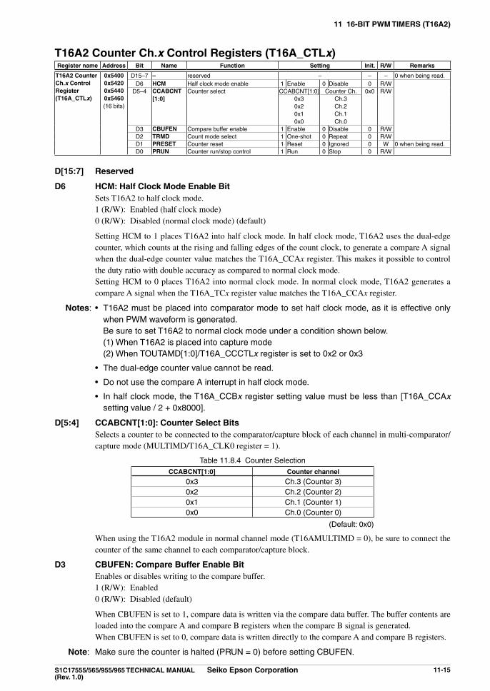
11 16-BiT PWM TiMeRS (T16a2)
S1C17555/565/955/965 TeChniCal Manual Seiko epson Corporation 11-15(Rev. 1.0)
T16a2 Counter Ch.x Control Registers (T16a_CTlx)Register name address Bit name Function Setting init. R/W Remarks
T16a2 Counter Ch.x Control Register(T16a_CTlx)
0x54000x54200x54400x5460(16 bits)
D15–7 – reserved – – – 0 when being read.D6 hCM Half clock mode enable 1 Enable 0 Disable 0 R/W
D5–4 CCaBCnT[1:0]
Counter select CCABCNT[1:0] Counter Ch. 0x0 R/W0x30x20x10x0
Ch.3Ch.2Ch.1Ch.0
D3 CBuFen Compare buffer enable 1 Enable 0 Disable 0 R/WD2 TRMD Count mode select 1 One-shot 0 Repeat 0 R/WD1 PReSeT Counter reset 1 Reset 0 Ignored 0 W 0 when being read.D0 PRun Counter run/stop control 1 Run 0 Stop 0 R/W
D[15:7] Reserved
D6 hCM: half Clock Mode enable Bit Sets T16A2 to half clock mode. 1 (R/W): Enabled (half clock mode) 0 (R/W): Disabled (normal clock mode) (default)
Setting HCM to 1 places T16A2 into half clock mode. In half clock mode, T16A2 uses the dual-edge counter, which counts at the rising and falling edges of the count clock, to generate a compare A signal when the dual-edge counter value matches the T16A_CCAx register. This makes it possible to control the duty ratio with double accuracy as compared to normal clock mode.
Setting HCM to 0 places T16A2 into normal clock mode. In normal clock mode, T16A2 generates a compare A signal when the T16A_TCx register value matches the T16A_CCAx register.
notes: • T16A2 must be placed into comparator mode to set half clock mode, as it is effective only when PWM waveform is generated.
Be sure to set T16A2 to normal clock mode under a condition shown below. (1) When T16A2 is placed into capture mode (2) When TOUTAMD[1:0]/T16A_CCCTLx register is set to 0x2 or 0x3
• The dual-edge counter value cannot be read.
• Do not use the compare A interrupt in half clock mode.
• In half clock mode, the T16A_CCBx register setting value must be less than [T16A_CCAx setting value / 2 + 0x8000].
D[5:4] CCaBCnT[1:0]: Counter Select Bits Selects a counter to be connected to the comparator/capture block of each channel in multi-comparator/
capture mode (MULTIMD/T16A_CLK0 register = 1).
8.4 Counter Selection Table 11.
CCaBCnT[1:0] Counter channel
0x3 Ch.3 (Counter 3)0x2 Ch.2 (Counter 2)0x1 Ch.1 (Counter 1)0x0 Ch.0 (Counter 0)
(Default: 0x0)
When using the T16A2 module in normal channel mode (T16AMULTIMD = 0), be sure to connect the counter of the same channel to each comparator/capture block.
D3 CBuFen: Compare Buffer enable Bit Enables or disables writing to the compare buffer. 1 (R/W): Enabled 0 (R/W): Disabled (default)
When CBUFEN is set to 1, compare data is written via the compare data buffer. The buffer contents are loaded into the compare A and compare B registers when the compare B signal is generated.
When CBUFEN is set to 0, compare data is written directly to the compare A and compare B registers.
note: Make sure the counter is halted (PRUN = 0) before setting CBUFEN.

11 16-BiT PWM TiMeRS (T16a2)
11-16 Seiko epson Corporation S1C17555/565/955/965 TeChniCal Manual (Rev. 1.0)
D2 TRMD: Count Mode Select Bit Selects the count mode. 1 (R/W): One-shot mode 0 (R/W): Repeat mode (default)
Setting TRMD to 0 sets the counter to repeat mode. In this mode, once the count starts, the counter con-tinues counting until stopped by the application program.
Setting TRMD to 1 sets the counter to one-shot mode. In this mode, the counter stops counting auto-matically as soon as the compare B signal is generated.
D1 PReSeT: Counter Reset Bit Resets the counter. 1 (W): Reset 0 (W): Ignored 0 (R): Normally 0 when read out (default)
Writing 1 to this bit resets the counter to 0. PRESET retains 1 during the reset period and reverts to 0 after the resetting has completed. The count clock must be supplied to the counter channel to be reset.
D0 PRun: Counter Run/Stop Control Bit Starts/stops the count. 1 (W): Run 0 (W): Stop 1 (R): Counting 0 (R): Stopped (default)
The counter starts counting when PRUN is written as 1 and stops when written as 0. The counter data is retained even if the counter is stopped.
T16a2 Counter Ch.x Data Registers (T16a_TCx)Register name address Bit name Function Setting init. R/W Remarks
T16a2 Counter Ch.x Data Register(T16a_TCx)
0x54020x54220x54420x5462(16 bits)
D15–0 T16aTC[15:0]
Counter dataT16ATC15 = MSBT16ATC0 = LSB
0x0 to 0xffff 0x0 R
D[15:0] T16aTC[15:0]: Counter Data Bits Counter data can be read out. (Default: 0x0) The counter value can be read out even if the counter is running. However, the counter value should be
read at once using a 16-bit transfer instruction. If data is read twice using an 8-bit transfer instruction, the correct value may not be obtained due to occurrence of count up between readings.
T16a2 Comparator/Capture Ch.x Control Registers (T16a_CCCTlx)Register name address Bit name Function Setting init. R/W Remarks
T16a2 Comparator/Capture Ch.x Control Register(T16a_CCCTlx)
0x54040x54240x54440x5464(16 bits)
D15–12 – reserved – 0x0 – Do not set to 1.D11–10 – reserved – – – 0 when being read.
D9–8 – reserved – 0 – Do not set to 1.D7–6 CaPaTRG
[1:0]Capture A trigger select CAPATRG[1:0] Trigger edge 0x0 R/W
0x30x20x10x0
↑ and ↓↓↑
NoneD5–4 TOuTaMD
[1:0]TOUTA mode select TOUTAMD[1:0] Mode 0x0 R/W
0x30x20x10x0
cmp B: ↑ or ↓cmp A: ↑ or ↓cmp A: ↑, B: ↓
OffD3–2 – reserved – – – 0 when being read.
D1 TOuTainV TOUTA invert 1 Invert 0 Normal 0 R/WD0 CCaMD T16A_CCA register mode select 1 Capture 0 Comparator 0 R/W
D[15:12] Reserved (Do not set to 1.)

11 16-BiT PWM TiMeRS (T16a2)
S1C17555/565/955/965 TeChniCal Manual Seiko epson Corporation 11-17(Rev. 1.0)
D[11:10] Reserved
D[9:8] Reserved (Do not set to 1.)
D[7:6] CaPaTRG[1:0]: Capture a Trigger Select Bits Selects the trigger edge(s) of the external signal (CAPAx) at which the counter value is captured in the
capture A register.
8.5 Capture A Trigger Edge SelectionTable 11.
CaPaTRG[1:0] Trigger edge
0x3 Falling edge and rising edge 0x2 Falling edge 0x1 Rising edge 0x0 Not triggered
(Default: 0x0)
CAPATRG[1:0] are control bits for capture mode and are ineffective in comparator mode.
D[5:4] TOuTaMD[1:0]: TOuTa Mode Select Bits Configures how the TOUTAx signal waveform is changed by the compare A and compare B signals.
These bits are also used to turn the TOUTAx output On and Off.
8.6 TOUT A Generation Mode Table 11.
TOuTaMD[1:0] When compare a occurs When compare B occurs
0x3 No change Toggle0x2 Toggle No change0x1 Rise Fall0x0 Disable output
(Default: 0x0)
TOUTAMD[1:0] are control bits for comparator mode and are ineffective in capture mode.
D[3:2] Reserved
D1 TOuTainV: TOuTa invert Bit Selects the TOUTAx signal polarity. 1 (R/W): Inverted (active Low) 0 (R/W): Normal (active High) (default)
Writing 1 to TOUTAINV generates an active Low signal (Off level = High) for the TOUTAx output. When TOUTAINV is 0, an active High signal (Off level = Low) is generated.
TOUTAINV is a control bit for comparator mode and is ineffective in capture mode.
D0 CCaMD: T16a_CCa Register Mode Select Bit Selects the T16A_CCAx register function (comparator mode or capture mode). 1 (R/W): Capture mode 0 (R/W): Comparator mode (default)
Writing 1 to CCAMD configures the T16A_CCAx register as the capture A register (capture mode) to which the counter data will be loaded by the external trigger signal. When CCAMD is 0, the T16A_CCAx register functions as the compare A register (comparator mode) for writing a comparison value to generate the compare A signal.
T16a2 Comparator/Capture Ch.x a Data Registers (T16a_CCax)Register name address Bit name Function Setting init. R/W Remarks
T16a2 Comparator/Capture Ch.x a Data Register(T16a_CCax)
0x54060x54260x54460x5466(16 bits)
D15–0 CCa[15:0] Compare/capture A dataCCA15 = MSBCCA0 = LSB
0x0 to 0xffff 0x0 R/W

11 16-BiT PWM TiMeRS (T16a2)
11-18 Seiko epson Corporation S1C17555/565/955/965 TeChniCal Manual (Rev. 1.0)
D[15:0] CCa[15:0]: Compare/Capture a Data Bits
In comparator mode (CCAMD/ T16A_CCCTLx register = 0) Sets a compare A data, which will be compared with the counter value, through this register. The counter value comparison timing varies according to the CBUFEN/T16A_CTLx register value. For
more information, see “Comparator mode (CCAMD = 0, default)” in Section 11.4.1.
In capture mode (CCAMD = 1) When the counter value is captured at the external trigger signal (CAPAx) edge selected using
CAPATRG[1:0]/T16A_CCCTLx register, the captured value is loaded to this register. At the same time a capture A interrupt can be generated, thus the captured counter value can be read out in the interrupt handler.
T16a2 Comparator/Capture Ch.x B Data Registers (T16a_CCBx)Register name address Bit name Function Setting init. R/W Remarks
T16a2 Comparator/Capture Ch.x B Data Register(T16a_CCBx)
0x54080x54280x54480x5468(16 bits)
D15–0 CCB[15:0] Compare B dataCCB15 = MSBCCB0 = LSB
0x0 to 0xffff 0x0 R/W
D[15:0] CCB[15:0]: Compare B Data Bits Sets a compare B data, which will be compared with the counter value, through this register. The counter value comparison timing varies according to the CBUFEN/T16A_CTLx register value. For
more information, see “Comparator mode (CCAMD = 0, default)” in Section 11.4.1.
T16a2 Comparator/Capture Ch.x interrupt enable Registers (T16a_ienx)Register name address Bit name Function Setting init. R/W Remarks
T16a2 Comparator/Capture Ch.x interrupt enable Register(T16a_ienx)
0x540a0x542a0x544a0x546a(16 bits)
D15–6 – reserved – – – 0 when being read.D5 – reserved – 0 – Do not set to 1.D4 CaPaOWie Capture A overwrite interrupt enable 1 Enable 0 Disable 0 R/WD3 – reserved – 0 – Do not set to 1.D2 CaPaie Capture A interrupt enable 1 Enable 0 Disable 0 R/WD1 CBie Compare B interrupt enable 1 Enable 0 Disable 0 R/WD0 Caie Compare A interrupt enable 1 Enable 0 Disable 0 R/W
D[15:6] Reserved
D5 Reserved (Do not set to 1.)
D4 CaPaOWie: Capture a Overwrite interrupt enable Bit Enables or disables capture A overwrite interrupts. 1 (R/W): Interrupt enabled 0 (R/W): Interrupt disabled (default)
Setting CAPAOWIE to 1 enables capture A overwrite interrupt requests to the ITC. Setting it to 0 dis-ables interrupts.
D3 Reserved (Do not set to 1.)
D2 CaPaie: Capture a interrupt enable Bit Enables or disables capture A interrupts. 1 (R/W): Interrupt enabled 0 (R/W): Interrupt disabled (default)
Setting CAPAIE to 1 enables capture A interrupt requests to the ITC. Setting it to 0 disables interrupts.
D1 CBie: Compare B interrupt enable Bit Enables or disables compare B interrupts. 1 (R/W): Interrupt enabled 0 (R/W): Interrupt disabled (default)
Setting CBIE to 1 enables compare B interrupt requests to the ITC. Setting it to 0 disables interrupts.
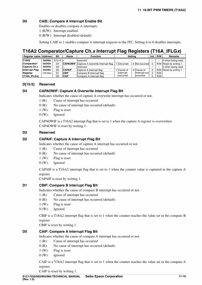
11 16-BiT PWM TiMeRS (T16a2)
S1C17555/565/955/965 TeChniCal Manual Seiko epson Corporation 11-19(Rev. 1.0)
D0 Caie: Compare a interrupt enable Bit Enables or disables compare A interrupts. 1 (R/W): Interrupt enabled 0 (R/W): Interrupt disabled (default)
Setting CAIE to 1 enables compare A interrupt requests to the ITC. Setting it to 0 disables interrupts.
T16a2 Comparator/Capture Ch.x interrupt Flag Registers (T16a_iFlGx)Register name address Bit name Function Setting init. R/W Remarks
T16a2 Comparator/Capture Ch.x interrupt Flag Register(T16a_iFlGx)
0x540c0x542c0x544c0x546c(16 bits)
D15–5 – reserved – – – 0 when being read.D4 CaPaOWiF Capture A overwrite interrupt flag 1 Occurred 0 Not occurred 0 R/W Reset by writing 1.D3 – reserved – – – 0 when being read.D2 CaPaiF Capture A interrupt flag 1 Cause of
interrupt occurred
0 Cause of interrupt not occurred
0 R/W Reset by writing 1.D1 CBiF Compare B interrupt flag 0 R/WD0 CaiF Compare A interrupt flag 0 R/W
D[15:5] Reserved
D4 CaPaOWiF: Capture a Overwrite interrupt Flag Bit Indicates whether the cause of capture A overwrite interrupt has occurred or not. 1 (R): Cause of interrupt has occurred 0 (R): No cause of interrupt has occurred (default) 1 (W): Flag is reset 0 (W): Ignored
CAPAOWIF is a T16A2 interrupt flag that is set to 1 when the capture A register is overwritten. CAPAOWIF is reset by writing 1.
D3 Reserved
D2 CaPaiF: Capture a interrupt Flag Bit Indicates whether the cause of capture A interrupt has occurred or not. 1 (R): Cause of interrupt has occurred 0 (R): No cause of interrupt has occurred (default) 1 (W): Flag is reset 0 (W): Ignored
CAPAIF is a T16A2 interrupt flag that is set to 1 when the counter value is captured in the capture A register.
CAPAIF is reset by writing 1.
D1 CBiF: Compare B interrupt Flag Bit Indicates whether the cause of compare B interrupt has occurred or not. 1 (R): Cause of interrupt has occurred 0 (R): No cause of interrupt has occurred (default) 1 (W): Flag is reset 0 (W): Ignored
CBIF is a T16A2 interrupt flag that is set to 1 when the counter reaches the value set in the compare B register.
CBIF is reset by writing 1.
D0 CaiF: Compare a interrupt Flag Bit Indicates whether the cause of compare A interrupt has occurred or not. 1 (R): Cause of interrupt has occurred 0 (R): No cause of interrupt has occurred (default) 1 (W): Flag is reset 0 (W): Ignored
CAIF is a T16A2 interrupt flag that is set to 1 when the counter reaches the value set in the compare A register.
CAIF is reset by writing 1.

12 ClOCK TiMeR (CT)
S1C17555/565/955/965 TeChniCal Manual Seiko epson Corporation 12-1(Rev. 1.0)
Clock Timer (CT)12
CT Module Overview12.1 The S1C17555/565/955/965 includes a clock timer module (CT) that uses the OSC1 oscillator as its clock source. This timer can be used for generating cyclic interrupts to implement a software clock function.The features of the CT module are listed below.
• 8-bit binary counter (128 Hz to 1 Hz)
• 32 Hz, 8 Hz, 2 Hz, and 1 Hz interrupts can be generated.
Figure 12.1.1 shows the CT configuration.
256 Hz
Inte
rnal
dat
a bu
s
Clock timer interrupt requestTo ITC
128Hz
64Hz
32Hz
16Hz
8Hz
4Hz
2Hz
1Hz
Count control circuit
Interrupt control circuit
Run/Stop control
Interruptenable
CTRUN
CTIE32CTIE8CTIE2CTIE1
Timer reset CTRST
CT_CNTD0 D1 D2 D3 D4 D5 D6 D7
Clock timerCLG
OSC1 oscillator/divider
1.1 CT ConfigurationFigure 12.
The CT module consists of an 8-bit binary counter that uses the 256 Hz signal divided from the OSC1 clock as the input clock and allows data for each bit (128 Hz to 1 Hz) to be read out by software. The clock timer can also gen-erate interrupts using the 32 Hz, 8 Hz, 2 Hz, and 1 Hz signals. This clock timer is normally used for various timing functions, such as a clock.
Operation Clock12.2 The CT module uses the 256 Hz clock output by the CLG module as the operation clock. The CLG module gener-ates this operation clock by dividing the OSC1 clock into 1/128, resulting in a frequency of 256 Hz when the OSC1 clock frequency is 32.768 kHz. The frequency described in this chapter will vary accordingly for other OSC1 clock frequencies.The CLG module does not include a 256 Hz clock output control bit. The 256 Hz clock is normally supplied to the clock timer when the OSC1 oscillation is on.For detailed information on OSC1 oscillator control, see the “Clock Generator (CLG)” chapter.
note: The OSC1 oscillator must be turned on before the CT module can operate.
Timer Reset12.3 Reset the timer by writing 1 to CTRST/CT_CTL register. This clears the counter to 0.Apart from this operation, the counter is also cleared by an initial reset.
Timer Run/STOP Control12.4 Make the following settings before starting CT.(1) If using interrupts, set the interrupt level and enable interrupts for the clock timer. See Section 12.5.(2) Reset the timer. See Section 12.3.
The clock timer includes CTRUN/CT_CTL register for Run/Stop control.

12 ClOCK TiMeR (CT)
12-2 Seiko epson Corporation S1C17555/565/955/965 TeChniCal Manual (Rev. 1.0)
The clock timer starts operating when 1 is written to CTRUN. Writing 0 to CTRUN disables clock input and stops the operation.This control does not affect the counter (CT_CNT register) data. The counter data is retained even when the count is halted, allowing resumption of the count from that data.If 1 is written to both CTRUN and CTRST simultaneously, the clock timer starts counting after resetting.A cause of interrupt occurs during counting at the 32 Hz, 8 Hz, 2 Hz, and 1 Hz signal falling edges. If interrupts are enabled, an interrupt request is sent to the interrupt controller (ITC).
256 Hz
128 Hz
64 Hz
32 Hz
16 Hz
8 Hz
4 Hz
2 Hz
1 Hz
32 Hz interrupt
8 Hz interrupt
2 Hz interrupt
1 Hz interrupt
OSC1/128
CTCNT0
CTCNT1
CTCNT2
CTCNT3
CTCNT4
CTCNT5
CTCNT6
CTCNT7
4.1 Clock Timer Timing ChartFigure 12.
notes: • The clock timer switches to Run/Stop status synchronized with the 256 Hz signal falling edge after data is written to CTRUN. When 0 is written to CTRUN, the timer stops after counting an additional “+1.” 1 is retained for CTRUN reading until the timer actually stops.
Figure 12.4.2 shows the Run/Stop control timing chart.
CTRUN(WR)
CT_CNT register 0x57 0x58 0x59 0x5a 0x5b 0x5c
CTRUN(RD)
256 Hz
4.2 Run/Stop Control Timing ChartFigure 12.
• Executing the slp instruction while the timer is running (CTRUN = 1) will destabilize the timer operation during restarting from SLEEP status. When switching to SLEEP status, stop the timer (CTRUN = 0) before executing the slp instruction.
CT interrupts12.5 The CT module includes functions for generating the following four kinds of interrupts:32 Hz, 8 Hz, 2 Hz, and 1 Hz interrupts
The CT module outputs a single interrupt signal shared by the above four interrupt causes to the interrupt controller (ITC). The interrupt flag in the CT module should be read to identify the cause of interrupt that occurred.
32 hz, 8 hz, 2 hz, and 1 hz interrupts The 32 Hz, 8 Hz, 2 Hz, and 1 Hz signal falling edges set the corresponding interrupt flag in the CT module to 1.
At the same time, an interrupt request is sent to the ITC if the corresponding interrupt enable bit has been set to 1 (interrupt enabled). An interrupt is generated if the ITC and S1C17 Core interrupt conditions are satisfied.
If the interrupt enable bit is set to 0 (interrupt disabled, default), no interrupt request will be sent to the ITC.

12 ClOCK TiMeR (CT)
S1C17555/565/955/965 TeChniCal Manual Seiko epson Corporation 12-3(Rev. 1.0)
5.1 CT Interrupt Flags and Interrupt Enable BitsTable 12.
Cause of interrupt interrupt flag interrupt enable bit
32 Hz Interrupt CTIF32/CT_IFLG register CTIE32/CT_IMSK register8 Hz Interrupt CTIF8/CT_IFLG register CTIE8/CT_IMSK register2 Hz Interrupt CTIF2/CT_IFLG register CTIE2/CT_IMSK register1 Hz Interrupt CTIF1/CT_IFLG register CTIE1/CT_IMSK register
For specific information on interrupt processing, see the “Interrupt Controller (ITC)” chapter.
notes: • The CT module interrupt flag must be reset in the interrupt handler routine after a CT interrupt has occurred to prevent recurring interrupts.
• Reset the interrupt flag before enabling CT interrupts with the interrupt enable bit to prevent occurrence of unwanted interrupt. The interrupt flag is reset by writing 1.
Control Register Details12.6 6.1 List of CT RegistersTable 12.
address Register name Function0x5000 CT_CTL Clock Timer Control Register Resets and starts/stops the timer.0x5001 CT_CNT Clock Timer Counter Register Counter data0x5002 CT_IMSK Clock Timer Interrupt Mask Register Enables/disables interrupt.
0x5003 CT_IFLG Clock Timer Interrupt Flag Register Indicates/resets interrupt occurrence status.
The CT registers are described in detail below.
note: When data is written to the registers, the “Reserved” bits must always be written as 0 and not 1.
Clock Timer Control Register (CT_CTl)Register name address Bit name Function Setting init. R/W Remarks
Clock Timer Control Register(CT_CTl)
0x5000(8 bits)
D7–5 – reserved – – – 0 when being read.D4 CTRST Clock timer reset 1 Reset 0 Ignored 0 W
D3–1 – reserved – – –D0 CTRun Clock timer run/stop control 1 Run 0 Stop 0 R/W
D[7:5] Reserved
D4 CTRST: Clock Timer Reset Bit Resets the clock timer. 1 (W): Reset 0 (W): Ignored 0 (R): Always 0 when read (default)
Writing 1 to this bit resets the counter to 0x0. When reset in Run state, the clock timer restarts immedi-ately after resetting. The reset data 0x0 is retained when in Stop state.
D[3:1] Reserved
D0 CTRun: Clock Timer Run/Stop Control Bit Controls the clock timer Run/Stop. 1 (R/W): Run 0 (R/W): Stop (default)
The clock timer starts counting when CTRUN is written as 1 and stops when written as 0. The counter data is retained at Stop state until a reset or the next Run state.
Clock Timer Counter Register (CT_CnT)Register name address Bit name Function Setting init. R/W Remarks
Clock Timer Counter Register(CT_CnT)
0x5001(8 bits)
D7–0 CTCnT[7:0] Clock timer counter value 0x0 to 0xff 0x0 R

12 ClOCK TiMeR (CT)
12-4 Seiko epson Corporation S1C17555/565/955/965 TeChniCal Manual (Rev. 1.0)
D[7:0] CTCnT[7:0]: Clock Timer Counter Value Bits The counter data can be read out. (Default: 0x0) This register is read-only and cannot be written to. The bits correspond to various frequencies, as follows: D7: 1 Hz, D6: 2 Hz, D5: 4 Hz, D4: 8 Hz, D3: 16 Hz, D2: 32 Hz, D1: 64 Hz, D0: 128 Hz
note: The correct counter value may not be read out (reading is unstable) if the register is read while counting is underway. Read the counter register twice in succession and treat the value as valid if the values read are identical.
Clock Timer interrupt Mask Register (CT_iMSK)Register name address Bit name Function Setting init. R/W Remarks
Clock Timer interrupt Mask Register(CT_iMSK)
0x5002(8 bits)
D7–4 – reserved – – – 0 when being read.D3 CTie32 32 Hz interrupt enable 1 Enable 0 Disable 0 R/WD2 CTie8 8 Hz interrupt enable 1 Enable 0 Disable 0 R/WD1 CTie2 2 Hz interrupt enable 1 Enable 0 Disable 0 R/WD0 CTie1 1 Hz interrupt enable 1 Enable 0 Disable 0 R/W
This register enables or disables interrupt requests individually for the 32 Hz, 8 Hz, 2 Hz, and 1 Hz signals. Setting CTIE* to 1 enables CT interrupts for the corresponding frequency signal falling edge, while setting to 0 disables interrupts.
D[7:4] Reserved
D3 CTie32: 32 hz interrupt enable Bit Enables or disables 32 Hz interrupts. 1 (R/W): Interrupt enabled 0 (R/W): Interrupt disabled (default)
D2 CTie8: 8 hz interrupt enable Bit Enables or disables 8 Hz interrupts. 1 (R/W): Interrupt enabled 0 (R/W): Interrupt disabled (default)
D1 CTie2: 2 hz interrupt enable Bit Enables or disables 2 Hz interrupts. 1 (R/W): Interrupt enabled 0 (R/W): Interrupt disabled (default)
D0 CTie1: 1 hz interrupt enable Bit Enables or disables 1 Hz interrupts. 1 (R/W): Interrupt enabled 0 (R/W): Interrupt disabled (default)
Clock Timer interrupt Flag Register (CT_iFlG)Register name address Bit name Function Setting init. R/W Remarks
Clock Timer interrupt Flag Register(CT_iFlG)
0x5003(8 bits)
D7–4 – reserved – – – 0 when being read.D3 CTiF32 32 Hz interrupt flag 1 Cause of
interrupt occurred
0 Cause of interrupt not occurred
0 R/W Reset by writing 1.D2 CTiF8 8 Hz interrupt flag 0 R/WD1 CTiF2 2 Hz interrupt flag 0 R/WD0 CTiF1 1 Hz interrupt flag 0 R/W
This register indicates the occurrence state of interrupt causes due to 32 Hz, 8 Hz, 2 Hz, and 1 Hz signals. If a CT interrupt occurs, identify the interrupt cause (frequency) by reading the interrupt flag in this register. CTIF* is a CT module interrupt flag that is set to 1 at the falling edge of the corresponding 32 Hz, 8 Hz, 2 Hz, or 1 Hz interrupt. CTIF* is reset by writing 1.
D[7:4] Reserved

12 ClOCK TiMeR (CT)
S1C17555/565/955/965 TeChniCal Manual Seiko epson Corporation 12-5(Rev. 1.0)
D3 CTiF32: 32 hz interrupt Flag Bit Indicates whether the cause of 32 Hz interrupt has occurred or not. 1 (R): Cause of interrupt has occurred 0 (R): No cause of interrupt has occurred (default) 1 (W): Flag is reset 0 (W): Ignored
D2 CTiF8: 8 hz interrupt Flag Bit Indicates whether the cause of 8 Hz interrupt has occurred or not. 1 (R): Cause of interrupt has occurred 0 (R): No cause of interrupt has occurred (default) 1 (W): Flag is reset 0 (W): Ignored
D1 CTiF2: 2 hz interrupt Flag Bit Indicates whether the cause of 2 Hz interrupt has occurred or not. 1 (R): Cause of interrupt has occurred 0 (R): No cause of interrupt has occurred (default) 1 (W): Flag is reset 0 (W): Ignored
D0 CTiF1: 1 hz interrupt Flag Bit Indicates whether the cause of 1 Hz interrupt has occurred or not. 1 (R): Cause of interrupt has occurred 0 (R): No cause of interrupt has occurred (default) 1 (W): Flag is reset 0 (W): Ignored

13 STOPWaTCh TiMeR (SWT)
S1C17555/565/955/965 TeChniCal Manual Seiko epson Corporation 13-1(Rev. 1.0)
Stopwatch Timer (SWT)13
SWT Module Overview13.1 The S1C17555/565/955/965 includes a 1/100-second stopwatch timer module (SWT) that uses the OSC1 oscillator as its clock source. This timer can be used to implement a software stopwatch function.The features of the SWT module are listed below.
• Two 4-bit BCD counters (approximately 1/100 and 1/10-second counters)
• Approximately 100 Hz, approximately 10 Hz, and 1 Hz interrupts can be generated.
Figure 13.1.1 shows the SWT configuration.
256 Hz
Inte
rnal
dat
a bu
s
Interrupt requestTo ITC
Feedbackdivider
1/100 s 4-bitBCD counter
1/10 s 4-bitBCD counter
Count control circuit
Interrupt control circuit
Run/Stop control
Interruptenable
SWTRUN
SIE100SIE10SIE1
Reset SWTRST
Stopwatch timerCLG
OSC1 oscillator/divider
Approx. 100 HzApprox. 10 Hz1 Hz
1.1 SWT ConfigurationFigure 13.
The SWT module consists of two 4-bit BCD counters (1/100 and 1/10 second) that use the 256 Hz signal divided from the OSC1 clock as the input clock and allows count data to be read out by software.The SWT module can also generate interrupts using the 100 Hz (approximately 100 Hz), 10 Hz (approximately 10 Hz), and 1 Hz signals.
Operation Clock13.2 The SWT module uses the 256 Hz clock output by the CLG module as the operation clock. The CLG module generates this operation clock by dividing the OSC1 clock into 1/128, resulting in a frequency of 256 Hz when the OSC1 clock frequency is 32.768 kHz. The frequency described in this chapter will vary accordingly for other OSC1 clock frequencies. The CLG module does not include a 256 Hz clock output control bit. The 256 Hz clock is normally supplied to the SWT module when the OSC1 oscillation is on.For detailed information on OSC1 oscillator control, see the “Clock Generator (CLG)” chapter.
note: The OSC1 oscillator must be turned on before the SWT module can operate.
BCD Counters13.3 The SWT module consists of 1/100-second and 1/10-second 4-bit BCD counters.The 1/100-second and 1/10-second counter values can be read from BCD100[3:0]/SWT_BCNT register and BCD10[3:0]/SWT_BCNT register, respectively.
Count-up Pattern A feedback divider is used to generate 100 Hz, 10 Hz, and 1 Hz signals from the 256 Hz clock. The counter
count-up pattern varies as shown in Figure 13.3.1.

13 STOPWaTCh TiMeR (SWT)
13-2 Seiko epson Corporation S1C17555/565/955/965 TeChniCal Manual (Rev. 1.0)
3256
2256
3256
2256
3256
2256
3256
2256
3256
2256
1/100-second counter count-up pattern 1
256 Hz
Approximate 100 Hz(Feedback divider output)
1/100-second counter
Approximate 10 Hz(1/100-second counter output)
Approximate 10 Hz(1/100-second counter output)
1/10-second counter
1 Hz(1/10-second counter output)
25256
1/100-second counter count-up pattern 2
s
26256
× 6 + 25256
× 4 = 1 s
26256
s 26256
s 25256
s 25256
s 26256
s 26256
s 25256
s 25256
s 26256
s 26256
s
s26256
3256
3256
3256
2256
3256
2256
3256
2256
3256
2256
0 1 2 3 4 5 6 7 8 9
0 1 2 3 4 5 6 7 8 9
0 1 2 3 4 5 6 7 8 9
1/10-second counter count-up pattern
3.1 SWT Count-Up PatternsFigure 13.
The feedback divider generates an approximate 100 Hz signal at 2/256-second and 3/256-second intervals from the 256 Hz signal supplied from the CLG module.
The 1/100-second counter counts the approximate 100 Hz signal output by the feedback divider and gener-ates an approximate 10 Hz signal at 25/256-second and 26/256-second intervals. Count-up will be pseudo 1/100-second counting at 2/256-second and 3/256-second intervals.
The 1/10-second counter counts the approximate 10 Hz signal generated by the 1/100-second counter at a ra-tio of 4:6, and generates a 1 Hz signal. Count-up will be pseudo 1/10-second counting at 25/256-second and 26/256-second intervals.
Timer Reset13.4 Reset the SWT module by writing 1 to SWTRST/SWT_CTL register. This clears the counter to 0.Apart from this operation, the counter is also cleared by initial reset.
Timer Run/STOP Control13.5 Make the following settings before starting SWT.(1) If using interrupts, set the interrupt level and enable interrupts for the SWT module. See Section 13.6.(2) Reset the timer. See Section 13.4.
The SWT module includes SWTRUN/SWT_CTL register for Run/Stop control.The timer starts operating when 1 is written to SWTRUN. Writing 0 to SWTRUN disables clock input and stops the operation. This control does not affect the counter (SWT_BCNT register) data. The counter data is retained even when the count is halted, allowing resumption of the count from that data. If 1 is written to both SWTRUN and SWTRST simultaneously, the timer starts counting after resetting.A cause of interrupt occurs during counting at the 100 Hz (approximate 100 Hz), 10 Hz (approximate 10 Hz), and 1 Hz signal falling edges. If interrupts are enabled, an interrupt request is sent to the interrupt controller (ITC).

13 STOPWaTCh TiMeR (SWT)
S1C17555/565/955/965 TeChniCal Manual Seiko epson Corporation 13-3(Rev. 1.0)
BCD100[0]
BCD100[1]
BCD100[2]
BCD100[3]
100 Hz interrupt
10 Hz interrupt
1/100-secondcounterBCD data
BCD10[0]
BCD10[1]
BCD10[2]
BCD10[3]
1 Hz interrupt
1/10-secondcounterBCD data
1 2 3 4 5 6 7 8 9 0 1 2 3 4 5 6 7 8 9 0 1 2 3 40
5.1 SWT Timing ChartFigure 13.
notes: • The timer switches to Run/Stop status synchronized with the 256 Hz signal falling edge after data is written to SWTRUN. When 0 is written to SWTRUN, the timer stops after counting an additional “+1.” 1 is retained for SWTRUN reading until the timer actually stops.
Figure 13.5.2 shows the Run/Stop control timing chart.
SWTRUN(WR)
SWT_BCNT register 27 28 29 30 31 32
SWTRUN(RD)
256 Hz
5.2 Run/Stop Control Timing ChartFigure 13.
• Executing the slp instruction while the timer is running (SWTRUN = 1) will destabilize the timer operation during restarting from SLEEP status. When switching to SLEEP status, stop the timer (SWTRUN = 0) before executing the slp instruction.
SWT interrupts13.6 The SWT module includes functions for generating the following three kinds of interrupts:100 Hz, 10 Hz, and 1 Hz interrupts
The SWT module outputs a single interrupt signal shared by the above three interrupt causes to the interrupt control-ler (ITC). The interrupt flag in the SWT module should be read to identify the cause of interrupt that occurred.
100 hz, 10 hz, 1 hz interrupts The 100 Hz (approximate 100 Hz), 10 Hz (approximate 10 Hz), and 1 Hz signal falling edges set the corre-
sponding interrupt flag in the SWT module to 1. At the same time, an interrupt request is sent to the ITC if the corresponding interrupt enable bit has been set to 1 (interrupt enabled). An interrupt is generated if the ITC and S1C17 Core interrupt conditions are satisfied.
If the interrupt enable bit is set to 0 (interrupt disabled, default), no interrupt request will be sent to the ITC.
6.1 SWT Interrupt Flags and Interrupt Enable BitsTable 13.
Cause of interrupt interrupt flag interrupt enable bit
100 Hz Interrupt SIF100/SWT_IFLG register SIE100/SWT_IMSK register10 Hz Interrupt SIF10/SWT_IFLG register SIE10/SWT_IMSK register1 Hz Interrupt SIF1/SWT_IFLG register SIE1/SWT_IMSK register
For specific information on interrupt processing, see the “Interrupt Controller (ITC)” chapter.

13 STOPWaTCh TiMeR (SWT)
13-4 Seiko epson Corporation S1C17555/565/955/965 TeChniCal Manual (Rev. 1.0)
notes: • The SWT module interrupt flag must be reset in the interrupt handler routine after a stopwatch timer interrupt has occurred to prevent recurring interrupts.
• Reset the interrupt flag before enabling SWT interrupts with the interrupt enable bit to prevent occurrence of unwanted interrupt. The interrupt flag is reset by writing 1.
Control Register Details13.7 7.1 List of SWT RegistersTable 13.
address Register name Function0x5020 SWT_CTL Stopwatch Timer Control Register Resets and starts/stops the timer.0x5021 SWT_BCNT Stopwatch Timer BCD Counter Register BCD counter data0x5022 SWT_IMSK Stopwatch Timer Interrupt Mask Register Enables/disables interrupt.
0x5023 SWT_IFLG Stopwatch Timer Interrupt Flag Register Indicates/resets interrupt occurrence status.
The SWT registers are described in detail below.
note: When data is written to the registers, the “Reserved” bits must always be written as 0 and not 1.
Stopwatch Timer Control Register (SWT_CTl)Register name address Bit name Function Setting init. R/W Remarks
Stopwatch Timer Control Register(SWT_CTl)
0x5020(8 bits)
D7–5 – reserved – – – 0 when being read.D4 SWTRST Stopwatch timer reset 1 Reset 0 Ignored 0 W
D3–1 – reserved – – –D0 SWTRun Stopwatch timer run/stop control 1 Run 0 Stop 0 R/W
D[7:5] Reserved
D4 SWTRST: Stopwatch Timer Reset Bit Resets the SWT module. 1 (W): Reset 0 (W): Ignored 0 (R): Always 0 when read (default)
Writing 1 to this bit resets the counter to 0x0. When reset in Run state, the timer restarts immediately after resetting. The reset data 0x0 is retained when in Stop state.
D[3:1] Reserved
D0 SWTRun: Stopwatch Timer Run/Stop Control Bit Controls the timer Run/Stop. 1 (R/W): Run 0 (R/W): Stop (default)
The timer starts counting when SWTRUN is written as 1 and stops when written as 0. The counter data is retained at Stop state until a reset or the next Run state.
Stopwatch Timer BCD Counter Register (SWT_BCnT)Register name address Bit name Function Setting init. R/W Remarks
Stopwatch Timer BCD Counter Register(SWT_BCnT)
0x5021(8 bits)
D7–4
BCD10[3:0] 1/10 sec. BCD counter value 0 to 9 0 R
D3–0
BCD100[3:0] 1/100 sec. BCD counter value 0 to 9 0 R
D[7:4] BCD10[3:0]: 1/10 Sec. BCD Counter Value Bits The 1/10-second counter BCD data can be read out. (Default: 0) This register is read-only and cannot be written to.
D[3:0] BCD100[3:0]: 1/100 Sec. BCD Counter Value Bits The 1/100-second counter BCD data can be read out. (Default: 0) This register is read-only and cannot be written to.

13 STOPWaTCh TiMeR (SWT)
S1C17555/565/955/965 TeChniCal Manual Seiko epson Corporation 13-5(Rev. 1.0)
note: The correct counter value may not be read out (reading is unstable) if the register is read while counting is underway. Read the counter register twice in succession and treat the value as valid if the values read are identical.
Stopwatch Timer interrupt Mask Register (SWT_iMSK)Register name address Bit name Function Setting init. R/W Remarks
Stopwatch Timer interrupt Mask Register(SWT_iMSK)
0x5022(8 bits)
D7–3 – reserved – – – 0 when being read.D2 Sie1 1 Hz interrupt enable 1 Enable 0 Disable 0 R/WD1 Sie10 10 Hz interrupt enable 1 Enable 0 Disable 0 R/WD0 Sie100 100 Hz interrupt enable 1 Enable 0 Disable 0 R/W
This register enables or disables interrupt requests individually for the 100 Hz, 10 Hz, and 1 Hz signals. Setting SIE* to 1 enables SWT interrupts for the corresponding frequency signal falling edge, while setting to 0 disables interrupts.
D[7:3] Reserved
D2 Sie1: 1 hz interrupt enable Bit Enables or disables 1 Hz interrupts. 1 (R/W): Interrupt enabled 0 (R/W): Interrupt disabled (default)
D1 Sie10: 10 hz interrupt enable Bit Enables or disables 10 Hz interrupts. 1 (R/W): Interrupt enabled 0 (R/W): Interrupt disabled (default)
D0 Sie100: 100 hz interrupt enable Bit Enables or disables 100 Hz interrupts. 1 (R/W): Interrupt enabled 0 (R/W): Interrupt disabled (default)
Stopwatch Timer interrupt Flag Register (SWT_iFlG)Register name address Bit name Function Setting init. R/W Remarks
Stopwatch Timer interrupt Flag Register(SWT_iFlG)
0x5023(8 bits)
D7–3 – reserved – – – 0 when being read.D2 SiF1 1 Hz interrupt flag 1 Cause of
interrupt occurred
0 Cause of interrupt not occurred
0 R/W Reset by writing 1.D1 SiF10 10 Hz interrupt flag 0 R/WD0 SiF100 100 Hz interrupt flag 0 R/W
This register indicates the occurrence state of interrupt causes due to 100 Hz, 10 Hz, and 1 Hz signals. If an SWT interrupt occurs, identify the interrupt cause (frequency) by reading the interrupt flag in this register. SIF* is an SWT module interrupt flag that is set to 1 at the falling edge of the corresponding 100 Hz, 10 Hz, or 1 Hz interrupt. SIF* is reset by writing 1.
D[7:3] Reserved
D2 SiF1: 1 hz interrupt Flag Bit Indicates whether the cause of 1 Hz interrupt has occurred or not. 1 (R): Cause of interrupt has occurred 0 (R): No cause of interrupt has occurred (default) 1 (W): Flag is reset 0 (W): Ignored
D1 SiF10: 10 hz interrupt Flag Bit Indicates whether the cause of 10 Hz interrupt has occurred or not. 1 (R): Cause of interrupt has occurred 0 (R): No cause of interrupt has occurred (default) 1 (W): Flag is reset 0 (W): Ignored

13 STOPWaTCh TiMeR (SWT)
13-6 Seiko epson Corporation S1C17555/565/955/965 TeChniCal Manual (Rev. 1.0)
D0 SiF100: 100 hz interrupt Flag Bit Indicates whether the cause of 100 Hz interrupt has occurred or not. 1 (R): Cause of interrupt has occurred 0 (R): No cause of interrupt has occurred (default) 1 (W): Flag is reset 0 (W): Ignored

14 WaTChDOG TiMeR (WDT)
S1C17555/565/955/965 TeChniCal Manual Seiko epson Corporation 14-1(Rev. 1.0)
Watchdog Timer (WDT)14
WDT Module Overview14.1 The S1C17555/565/955/965 includes a watchdog timer module (WDT) used to detect CPU runaway.The features of WDT are listed below.
• 10-bit up counter
• Either reset or NMI can be generated if the counter overflows.
Figure 14.1.1 shows the WDT configuration.
NMIReset
10-bit counter
Interrupt control circuit
Run/Stop control
NMI/resetmode select
WDTRUN[3:0]
WDTMD
Watchdog timer reset WDTRST
Watchdog timer
WDTCLK
Clock enable
Division ratioselection
Clock sourceselection
CLKEN
CLKDIV[1:0] CLKSRC[1:0]
OSC1 clock
OSC3 clock Divider(1/4K–1/32K)
IOSC clock Divider(1/4K–1/32K)
S1C17565/965
Divider(1/128)
1.1 WDT ConfigurationFigure 14.
The WDT module generates an NMI or reset (selectable via software) to the CPU if not reset within 1,024/fWDTCLK seconds (4 seconds when the clock source is OSC1).Reset WDT via software within this cycle to prevent NMI/resets, which in turn enables runaway detection for pro-grams that do not pass through the handler routine.
Operation Clock14.2 The WDT module includes a clock source selector, dividers, and a gate circuit for controlling the operation clock.
Clock source selection Use CLKSRC[1:0]/WDT_CLK register to select the clock source from IOSC, OSC3 (S1C17565/965), and
OSC1.
2.1 Clock Source SelectionTable 14.
ClKSRC[1:0]Clock source
S1C17555/955 S1C17565/965
0x3 Reserved0x2 Reserved OSC30x1 OSC1 OSC10x0 IOSC IOSC
(Default: 0x0)
Clock division ratio selection When the clock source is OSC1
No division ratio needs to be selected when OSC1 is selected for the clock source. The WDTCLK is gener-ated by dividing the OSC1 clock by 128.
When the clock source is IOSC or OSC3 When IOSC or OSC3 is selected for the clock source, use CLKDIV[1:0]/WDT_CLK register to select the
division ratio.

14 WaTChDOG TiMeR (WDT)
14-2 Seiko epson Corporation S1C17555/565/955/965 TeChniCal Manual (Rev. 1.0)
2.2 IOSC/OSC3 Division Ratio SelectionTable 14.
ClKDiV[1:0] Division ratio
0x3 1/327680x2 1/163840x1 1/81920x0 1/4096
(Default: 0x0)
Clock enable The clock supply is enabled with CLKEN/WDT_CLK register. The CLKEN default setting is 0, which stops
the clock. Setting CLKEN to 1 feeds the clock generated as above to the WDT circuit. If no WDT operation is required, stop the clock to reduce current consumption.
WDT Control14.3
nMi/Reset Mode Selection14.3.1
WDTMD/WDT_ST register is used to select whether an NMI signal or a reset signal is output when WDT has not been reset within the NMI/reset generation cycle.To generate an NMI, set WDTMD to 0 (default). Set to 1 to generate a reset.
WDT Run/Stop Control14.3.2
WDT starts counting when a value other than 0b1010 is written to WDTRUN[3:0]/WDT_CTL register and stops when 0b1010 is written.At initial reset, WDTRUN[3:0] is set to 0b1010 to stop the watchdog timer.Since an NMI or reset may be generated immediately after running depending on the counter value, WDT should also be reset concurrently (before running the watchdog timer), as explained in the following section.
WDT Reset14.3.3
To reset WDT, write 1 to WDTRST/WDT_CTL register.A location should be provided for periodically processing the routine for resetting WDT before an NMI or reset is generated when using WDT. Process this routine within 1,024/fWDTCLK seconds (4 seconds when the clock source is OSC1) cycle.After resetting, WDT starts counting with a new NMI/Reset generation cycle.If WDT is not reset within the NMI/Reset generation cycle for any reason, the CPU is switched to interrupt pro-cessing by NMI or reset, the interrupt vector is read out, and the interrupt handler routine is executed. The reset and NMI vector addresses are TTBR + 0x0 and TTBR + 0x08.
If the counter overflows and generates an NMI without WDT being reset, WDTST/WDT_ST register is set to 1. This bit is provided to confirm that WDT was the source of the NMI. The WDTST set to 1 is cleared to 0 by reset-ting WDT.
Operations in halT and SleeP Modes14.3.4
halT mode The WDT module operates in HALT mode, as the clock is supplied. HALT mode is therefore cleared by an NMI or
reset if it continues for more than the NMI/reset generation cycle. To disable WDT while in HALT mode, stop WDT by writing 0b1010 to WDTRUN[3:0]/WDT_CTL register before executing the halt instruction. Reset WDT before resuming operations after HALT mode is cleared.

14 WaTChDOG TiMeR (WDT)
S1C17555/565/955/965 TeChniCal Manual Seiko epson Corporation 14-3(Rev. 1.0)
SleeP mode The clock supplied from the CLG module is stopped in SLEEP mode, which also stops WDT. To prevent generation
of an unnecessary NMI or reset after clearing SLEEP mode, reset WDT before executing the slp instruction. WDT should also be stopped as required using WDTRUN[3:0].
Control Register Details14.4 Table 14.4.1 List of WDT Registers
address Register name Function0x5040 WDT_CTL Watchdog Timer Control Register Resets and starts/stops the timer.0x5041 WDT_ST Watchdog Timer Status Register Sets the timer mode and indicates NMI status.0x5070 WDT_CLK WDT Clock Control Register Controls the WDT clock.
The WDT registers are described in detail below.
note: When data is written to the registers, the “Reserved” bits must always be written as 0 and not 1.
Watchdog Timer Control Register (WDT_CTl)Register name address Bit name Function Setting init. R/W Remarks
Watchdog Timer Control Register(WDT_CTl)
0x5040(8 bits)
D7–5 – reserved – – – 0 when being read.D4 WDTRST Watchdog timer reset 1 Reset 0 Ignored 0 W
D3–0 WDTRun[3:0] Watchdog timer run/stop control
Other than 1010Run
1010Stop
1010 R/W
D[7:5] Reserved
D4 WDTRST: Watchdog Timer Reset Bit Resets WDT. 1 (W): Reset 0 (W): Ignored 0 (R): Always 0 when read (default)
note: To use WDT, it must be reset by writing 1 to this bit within the NMI/reset generation cycle (4 seconds when fOSC1 = 32.768 kHz). This resets the up-counter to 0 and starts counting with a new NMI/reset generation cycle.
D[3:0] WDTRun[3:0]: Watchdog Timer Run/Stop Control Bits Controls WDT Run/Stop. Values other than 0b1010 (R/W): Run 0b1010 (R/W): Stop (default)
note: WDT must also be reset to prevent generation of an unnecessary NMI or Reset before start-ing WDT.
Watchdog Timer Status Register (WDT_ST)Register name address Bit name Function Setting init. R/W Remarks
Watchdog Timer Status Register(WDT_ST)
0x5041(8 bits)
D7–2 – reserved – – – 0 when being read.
D1 WDTMD NMI/Reset mode select 1 Reset 0 NMI 0 R/WD0 WDTST NMI status 1 NMI occurred 0 Not occurred 0 R
D[7:2] Reserved
D1 WDTMD: nMi/Reset Mode Select Bit Selects NMI or reset generation on counter overflow. 1 (R/W): Reset 0 (R/W): NMI (default)
Setting this bit to 1 outputs a reset signal when the counter overflows. Setting to 0 outputs an NMI sig-nal.

14 WaTChDOG TiMeR (WDT)
14-4 Seiko epson Corporation S1C17555/565/955/965 TeChniCal Manual (Rev. 1.0)
D0 WDTST: nMi Status Bit Indicates a counter overflow and NMI occurrence. 1 (R): NMI occurred (counter overflow) 0 (R): NMI not occurred (default)
This bit confirms that WDT was the source of the NMI. The WDTST set to 1 is cleared to 0 by resetting WDT.
This is also set by a counter overflow if reset output is selected, but is cleared by initial reset and cannot be confirmed.
WDT Clock Control Register (WDT_ClK)Register name address Bit name Function Setting init. R/W Remarks
WDT Clock Control Register(WDT_ClK)
0x5070(8 bits)
D7–6 – reserved – – – 0 when being read.D5–4 ClKDiV
[1:0]Clock division ratio select CLKDIV[1:0] Division ratio 0x0 R/W When the clock
source is IOSC or OSC3
0x30x20x10x0
1/327681/163841/81921/4096
D3–2 ClKSRC[1:0]
Clock source select CLKSRC[1:0] Clock source 0x0 R/W * S1C17565/965 only0x3
0x20x10x0
reservedOSC3*OSC1IOSC
D1 – reserved – – – 0 when being read.D0 ClKen Count clock enable 1 Enable 0 Disable 0 R/W
D[7:6] Reserved
D[5:4] ClKDiV[1:0]: Clock Division Ratio Select Bits Selects the division ratio for generating the WDT clock when IOSC or OSC3 is used as the clock
source.
4.2 IOSC/OSC3 Division Ratio SelectionTable 14.
ClKDiV[1:0] Division ratio
0x3 1/327680x2 1/163840x1 1/81920x0 1/4096
(Default: 0x0)
D[3:2] ClKSRC[1:0]: Clock Source Select Bits Selects the WDT clock source.
4.3 Clock Source SelectionTable 14.
ClKSRC[1:0]Clock source
S1C17555/955 S1C17565/965
0x3 Reserved0x2 Reserved OSC30x1 OSC1 OSC10x0 IOSC IOSC
(Default: 0x0)
D1 Reserved
D0 ClKen: Count Clock enable Bit Enables or disables the clock supply to WDT. 1 (R/W): Enabled (on) 0 (R/W): Disabled (off) (default)
The CLKEN default setting is 0, which disables the clock supply. Setting CLKEN to 1 sends the clock selected to the WDT circuit.

15 uaRT
S1C17555/565/955/965 TeChniCal Manual Seiko epson Corporation 15-1(Rev. 1.0)
UART15 note: UART Ch.0 only is available in the S1C17555/955.
uaRT Module Overview15.1 The S1C17565/965 includes a UART module with two asynchronous communication channels and the S1C17555/955 includes one asynchronous communication channel. A UART channel includes a 2-byte receive data buffer and 1-byte transmit data buffer allowing successive data transfer. The UART module also includes an RZI modulator/demodulator circuit that enables IrDA 1.0-compatible infrared communications simply by adding basic external circuits.The following shows the main features of the UART:
• Transfer rate: 150 to 960 kbps (150 to 115,200 bps in IrDA mode)
• Transfer clock: Internal clock (baud rate generator output) or an external clock (SCLK input) can be selected.
• Character length: 7 or 8 bits (LSB first)
• Parity mode: Even, odd, or no parity
• Stop bit: 1 or 2 bits
• Start bit: 1 bit fixed
• Supports full-duplex communications.
• Includes a 2-byte receive data buffer and a 1-byte transmit data buffer.
• Includes a baud rate generator with fine adjustment function.
• Includes an RZI modulator/demodulator circuit to support IrDA 1.0-compatible infrared communications.
• Can detect parity error, framing error, and overrun error during receiving.
• Can generate receive buffer full, transmit buffer empty, end of transmission and receive error interrupts.
Figure 15.1.1 shows the UART configuration.
Shift registerReceive data
buffer (2 bytes)
Internal bus
ITC
UART Ch.x
Bus I/Fand
controlregisters
Shift registerTransmit data buffer (1 byte)
Clock/transfer control
RZIdemodulator
RZImodulator
Interruptcontrol
sclkBaud rate generator
Ch.0: SIN0 Ch.1: SIN1*
Ch.0: SCLK0Ch.1: SCLK1*
Ch.0: SOUT0Ch.1: SOUT1*
∗ Available only in S1C17565/965
Figure 15.1.1 UART Configuration
note: Two channels in the UART module have the same functions except for control register addresses. For this reason, the description in this chapter applies to both UART channels. The ‘x’ in the regis-ter name indicates the channel number (0 or 1).
Example: UART_CTLx register Ch.0: UART_CTL0 register Ch.1: UART_CTL1 register

15 uaRT
15-2 Seiko epson Corporation S1C17555/565/955/965 TeChniCal Manual (Rev. 1.0)
uaRT input/Output Pins15.2 Table 15.2.1 lists the UART input/output pins.
2.1 List of UART PinsTable 15.
Pin name i/O Qty Function
SIN0 (Ch.0)SIN1 (Ch.1)*
I 2 UART Ch.x data input pinInputs serial data sent from an external serial device.
SOUT0 (Ch.0)SOUT1 (Ch.1)*
O 2 UART Ch.x data output pinOutputs serial data sent to an external serial device.
SCLK0 (Ch.0)SCLK1 (Ch.1)*
I 2 UART Ch.x clock input pinInputs the transfer clock when an external clock is used.
* Available only in the S1C17565/965
The UART input/output pins (SINx, SOUTx, SCLKx) are shared with I/O ports and are initially set as general pur-pose I/O port pins. The pin functions must be switched using the port function select bits to use the general purpose I/O port pins as UART input/output pins.For detailed information on pin function switching, see the “I/O Ports (P)” chapter.
Baud Rate Generator15.3 The UART module includes a baud rate generator to generate the transfer (sampling) clock. It consists of an 8-bit programmable timer with fine mode. The timer counts down from the initial value set via software and outputs an underflow signal when the counter underflows. The underflow signal is used to generate the transfer clock. The un-derflow cycle can be programmed by selecting the clock source and initial data, enabling the application program to obtain serial transfer rates as required. Fine mode provides a function that minimizes transfer rate errors.
S1C17565/965
Baud rate registerUART_BRx
Underflow
Fine mode setting
Clock enable
ct_clk
Division ratioselection
Clock sourceselection
Down counter
Control circuit
FMD[3:0]
CLKEN
CLKDIV[1:0] CLKSRC[1:0]
Baud rate generator for UART Ch.x
OSC1 clock
External clock (SCLKx)
OSC3 clock Divider(1/1–1/8)
IOSC clock Divider(1/1–1/8)
Serial transfer clocksclk
sclk161/16
3.1 Baud Rate GeneratorFigure 15.
Clock source settings The clock source can be selected from IOSC, OSC3 (S1C17565/965), OSC1, or external clock using CLK-
SRC[1:0]/UART_CLKx register.
3.1 Clock Source SelectionTable 15.
ClKSRC[1:0]Clock source
S1C17555/955 S1C17565/965
0x3 Reserved0x2 Reserved OSC30x1 OSC1 OSC10x0 IOSC IOSC
(Default: 0x0)
note: When inputting the external clock via the SCLKx pin, the clock duty ratio must be 50%.
When IOSC or OSC3 is selected as the clock source, use CLKDIV[1:0]/UART_CLKx register to select the di-vision ratio.

15 uaRT
S1C17555/565/955/965 TeChniCal Manual Seiko epson Corporation 15-3(Rev. 1.0)
3.2 IOSC/OSC3 Division Ratio SelectionTable 15.
ClKDiV[1:0] Division ratio
0x3 1/80x2 1/40x1 1/20x0 1/1
(Default: 0x0)
Clock supply to the counter is controlled using CLKEN/UART_CLKx register. The CLKEN default setting is 0, which disables the clock supply. Setting CLKEN to 1 sends the clock selected to the counter.
initial counter value setting BR[7:0]/UART_BRx register is used to set the initial value for the down counter. The initial counter value is preset to the down counter if the counter underflows. This means that the initial
counter value and the count clock frequency determine the time elapsed between underflows.
Underflow signal/Baud rate generator output (sclk16)
Baud rate generator output (sclk)
1 2 3 8 16
3.2 Counter Underflow and Clock GeneratedFigure 15.
Use the following equations to calculate the initial counter value for obtaining the desired transfer rate.
ct_clkbps = ———————————— {(BR + 1) × 16 + FMD} ct_clkBR = (——— - FMD - 16) ÷ 16 bps
ct_clk: Count clock frequency (Hz)BR: BR[7:0] setting (0 to 255)bps: Transfer rate (bit/s)FMD: FMD[3:0] (fine mode) setting (0 to 15)
note: The UART transfer rate is capped at 960 kbps (115,200 bps in IrDA mode). Do not set faster transfer rates.
Fine Mode Fine mode provides a function that minimizes transfer rate errors. The baud rate generator output clock can be
set to the required frequency by selecting the appropriate clock source and initial counter data. Note that errors may occur, depending on the transfer rate. Fine mode extends the output clock cycle by delaying the underflow pulse from the counter. This delay can be specified with the FMD[3:0]/UART_FMDx register. FMD[3:0] speci-fies the delay pattern to be inserted into a 16 underflow period. Inserting one delay extends the output clock cycle by one count clock cycle.
3.3 Delay Patterns Specified by FMD[3:0]Table 15.
FMD[3:0] underflow number1 2 3 4 5 6 7 8 9 10 11 12 13 14 15 16
0x0 – – – – – – – – – – – – – – – –0x1 – – – – – – – – – – – – – – – D0x2 – – – – – – – D – – – – – – – D0x3 – – – – – – – D – – – D – – – D0x4 – – – D – – – D – – – D – – – D0x5 – – – D – – – D – – – D – D – D0x6 – – – D – D – D – – – D – D – D0x7 – – – D – D – D – D – D – D – D0x8 – D – D – D – D – D – D – D – D0x9 – D – D – D – D – D – D – D D D0xa – D – D – D D D – D – D – D D D0xb – D – D – D D D – D D D – D D D0xc – D D D – D D D – D D D – D D D0xd – D D D – D D D – D D D D D D D0xe – D D D D D D D – D D D D D D D0xf – D D D D D D D D D D D D D D D
D: Indicates the insertion of a delay cycle.
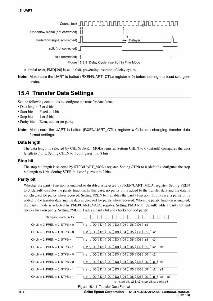
15 uaRT
15-4 Seiko epson Corporation S1C17555/565/955/965 TeChniCal Manual (Rev. 1.0)
Count clock
Underflow signal (not corrected)
Underflow signal (corrected)
sclk (not corrected)
sclk (corrected)
Delayed
15 16
15 16
1
1
3.3 Delay Cycle Insertion in Fine ModeFigure 15.
At initial reset, FMD[3:0] is set to 0x0, preventing insertion of delay cycles.
note: Make sure the UART is halted (RXEN/UART_CTLx register = 0) before setting the baud rate gen-erator.
Transfer Data Settings15.4 Set the following conditions to configure the transfer data format.• Data length: 7 or 8 bits• Start bit: Fixed at 1 bit• Stop bit: 1 or 2 bits• Parity bit: Even, odd, or no parity
note: Make sure the UART is halted (RXEN/UART_CTLx register = 0) before changing transfer data format settings.
Data length The data length is selected by CHLN/UART_MODx register. Setting CHLN to 0 (default) configures the data
length to 7 bits. Setting CHLN to 1 configures it to 8 bits.
Stop bit The stop bit length is selected by STPB/UART_MODx register. Setting STPB to 0 (default) configures the stop
bit length to 1 bit. Setting STPB to 1 configures it to 2 bits.
Parity bit Whether the parity function is enabled or disabled is selected by PREN/UART_MODx register. Setting PREN
to 0 (default) disables the parity function. In this case, no parity bit is added to the transfer data and the data is not checked for parity when received. Setting PREN to 1 enables the parity function. In this case, a parity bit is added to the transfer data and the data is checked for parity when received. When the parity function is enabled, the parity mode is selected by PMD/UART_MODx register. Setting PMD to 0 (default) adds a parity bit and checks for even parity. Setting PMD to 1 adds a parity bit and checks for odd parity.
Sampling clock (sclk)
CHLN = 0, PREN = 0, STPB = 0
CHLN = 0, PREN = 1, STPB = 0
CHLN = 0, PREN = 0, STPB = 1
CHLN = 0, PREN = 1, STPB = 1
CHLN = 1, PREN = 0, STPB = 0
CHLN = 1, PREN = 1, STPB = 0
CHLN = 1, PREN = 0, STPB = 1
CHLN = 1, PREN = 1, STPB = 1
s1 D0 D1 D2 D3 D4 D5 D6 s2
s1 D0 D1 D2 D3 D4 D5 D6 p s2
s1 D0 D1 D2 D3 D4 D5 D6 s2 s3
s1 D0 D1 D2 D3 D4 D5 D6 p s2 s3
s1 D0 D1 D2 D3 D4 D5 D6 D7 s2
s1 D0 D1 D2 D3 D4 D5 D6 D7 p s2
s1 D0 D1 D2 D3 D4 D5 D6 D7 s2 s3
s1 D0 D1 D2 D3 D4 D5 D6 D7 p s2 s3
s1: start bit, s2 & s3: stop bit, p: parity bit
Figure 15.4.1 Transfer Data Format

15 uaRT
S1C17555/565/955/965 TeChniCal Manual Seiko epson Corporation 15-5(Rev. 1.0)
Data Transfer Control15.5 Make the following settings before starting data transfers.(1) Select the input clock. (See Section 15.3.)(2) Program the baud rate generator to output the transfer clock. (See Section 15.3.)(3) Set the transfer data format. (See Section 15.4.)(4) To use the IrDA interface, set IrDA mode. (See Section 15.8.)(5) Set interrupt conditions to use UART interrupts. (See Section 15.7.)
note: Make sure the UART is halted (RXEN/UART_CTLx register = 0) before changing the above set-tings.
enabling data transfers Set RXEN/UART_CTLx register to 1 to enable data transfers. This puts the transmitter/receiver circuit in ready-
to-transmit/receive status.
note: Do not set RXEN to 0 while the UART is sending or receiving data.
Data transmission control To start data transmission, write the transmit data to TXD[7:0]/UART_TXDx register. The data is written to the transmit data buffer, and the transmitter circuit starts sending data. The buffer data is sent to the transmit shift register, and the start bit is output from the SOUTx pin. The data in
the shift register is then output from the LSB. The transfer data bit is shifted in sync with the sampling clock rising edge and output in sequence via the SOUTx pin. Following output of MSB, the parity bit (if parity is en-abled) and the stop bit are output.
The transmitter circuit includes three status flags: TDBE/UART_STx register, TRBS/UART_STx register, and TRED/UART_STx register.
The TDBE flag indicates the transmit data buffer status. This flag switches to 0 when the application program writes data to the transmit data buffer and reverts to 1 when the buffer data is sent to the transmit shift register. An interrupt can be generated when this flag is set to 1 (see Section 15.7). Subsequent data is sent after con-firming that the transmit data buffer is empty either by using this interrupt or by reading the TDBE flag. The transmit data buffer size is 1 byte, but a shift register is provided separately to allow data to be written while the previous data is being sent. Always confirm that the transmit data buffer is empty before writing transmit data. Writing data while the TDBE flag is 0 will overwrite earlier transmit data inside the transmit data buffer.
The TRBS flag indicates the shift register status. This flag switches to 1 when transmit data is loaded from the transmit data buffer to the shift register and reverts to 0 once the data is sent. Read this flag to check whether the transmitter circuit is operating or at standby.
The TRED switches to 1 when the TRBS flag reverts to 0 from 1, indicating that transmit operation has com-pleted. An interrupt can be generated when this flag is set to 1 (see Section 15.7). Use this interrupt for trans-mission end processing. The TRED flag is reset by writing 1.
S1: Start bit, S2: Stop bit, P: Parity bit, Wr: Data write to transmit data buffer
Sampling clock (sclk)
SOUTx
TDBE
TRBS
TRED
Interrupt
S1 D0 D1 D2 D3 D4 D5 D6 D7 P S2 S1 D0 D1 D7 P S2 S1 D0 D1 D7 P
Wr Wr Wr
S2
Transmit buffer empty interrupt requestEnd of transmission
interrupt request
5.1 Data Transmission Timing ChartFigure 15.

15 uaRT
15-6 Seiko epson Corporation S1C17555/565/955/965 TeChniCal Manual (Rev. 1.0)
Data reception control The receiver circuit is activated by setting RXEN to 1, enabling data to be received from an external serial de-
vice. When the external serial device sends a start bit, the receiver circuit detects its Low level and starts sampling
the following data bits. The data bits are sampled at the sampling clock rising edge, and the lead bit is loaded into the receive shift register as LSB. Once the MSB has been received into the shift register, the received data is loaded into the receive data buffer. If parity checking is enabled, the receiver circuit checks the received data at the same time by checking the parity bit received immediately after the MSB.
The receive data buffer, a 2-byte FIFO, receives data until full.
Received data in the buffer can be read from RXD[7:0]/UART_RXDx register. The oldest data is read out first and data is cleared by reading.
The receiver circuit includes two buffer status flags: RDRY/UART_STx register and RD2B/UART_STx regis-ter.
The RDRY flag indicates that the receive data buffer still contains data. The RD2B flag indicates that the re-ceive data buffer is full.
(1) RDRY = 0, RD2B = 0 The receive data buffer contents need not be read, since no data has been received.
(2) RDRY = 1, RD2B = 0 One 8-bit data has been received. Read the receive data buffer contents once. This resets the RDRY flag.
The buffer reverts to state (1) above. If the receive data buffer contents are read twice, the second data read will be invalid.
(3) RDRY = 1, RD2B = 1 Two 8-bit data have been received. Read the receive data buffer contents twice. The receive data buffer
outputs the oldest data first. This resets the RD2B flag. The buffer then reverts to the state in (2) above. The second read outputs the most recent received data, after which the buffer reverts to the state in (1) above.
Even when the receive data buffer is full, the shift register can start receiving 8-bit data one more time. An overrun error will occur if receiving is finished before the receive data buffer has been read. In this case, the last received data cannot be read. The contents of the receive data buffer must be read out before an overrun error occurs. For detailed information on overrun errors, refer to Section 15.6.
The volume of data received can be checked by reading these flags. The UART allows receive buffer full interrupts to be generated once data has been received in the receive data
buffer. These interrupts can be used to read the receive data buffer. By default, a receive buffer full interrupt occurs when the receive data buffer receives one 8-bit data (status (2) above). This can be changed by setting RBFI/UART_CTLx register to 1 so that an interrupt occurs when the receive data buffer receives two 8-bit data.
Three error flags are also provided in addition to the flags previously mentioned. See Section 15.6 for detailed information on flags and receive errors.

15 uaRT
S1C17555/565/955/965 TeChniCal Manual Seiko epson Corporation 15-7(Rev. 1.0)
Receive buffer full interrupt request(RBFI = 0)
Overrun error interrupt request
Sampling clock (sclk)
SINx
Receive data buffer
RDRY
RD2B
RXD[7:0]
Interrupt
data 1S1 D0 ··· P S2 S1 D0 ··· P S2 S1 D0 ··· P S2 S1 D0 ··· P S2 S1 D0 ··· P S2 S1 D0 ··· P S2
data 2 data 3 data 4 data 5 data 6
Rd
Rd
data 3, 4data 2data 1 – data 2, 3 data 3
data 3data 2data 1
S1: Start bit, S2: Stop bit, P: Parity bit, Rd: Data read from RXD[7:0]
5.2 Data Receiving Timing ChartFigure 15.
Disabling data transfers After a data transfer is completed (both transmission and reception), write 0 to RXEN to disable data transfers.
note: Setting RXEN to 0 empties the transmit data buffer, clearing any remaining data. The data being transferred cannot be guaranteed if RXEN is set to 0 while data is being sent or received.
Make sure that the TDBE flag is 1 and the TRBS and RDRY flags are both 0 before disabling data transfer.
Receive errors15.6 Three different receive errors may be detected while receiving data.Since receive errors are interrupt causes, they can be processed by generating interrupts. For more information on UART interrupt control, see Section 15.7.
Parity error If PREN/UART_MODx register has been set to 1 (parity enabled), data received is checked for parity. Data received in the shift register is checked for parity when sent to the receive data buffer. The matching is
checked against the PMD/UART_MODx register setting (odd or even parity). If the result is a non-match, a parity error is issued, and the parity error flag PER/UART_STx register is set to 1. Even if this error occurs, the data received is sent to the receive data buffer, and the receiving operation continues. However, the received data cannot be guaranteed if a parity error occurs. The PER flag is reset to 0 by writing 1.
Framing error A framing error occurs if the stop bit is received as 0 and the UART determines loss of sync. If the stop bit is
set to two bits, only the first bit is checked. The framing error flag FER/UART_STx register is set to 1 if this error occurs. The received data is still trans-
ferred to the receive data buffer if this error occurs and the receiving operation continues, but the data cannot be guaranteed, even if no framing error occurs for subsequent data receiving. The FER flag is reset to 0 by writing 1.
Overrun error Even if the receive data buffer is full (two 8-bit data already received), the third data can be received in the shift
register. However, if the receive data buffer is not emptied (by reading out data received) by the time this data has been received, the third data received in the shift register will not be sent to the buffer and an overrun error will be generated. If an overrun error occurs, the overrun error flag OER/UART_STx register is set to 1. The receiving operation continues even if this error occurs. The OER flag is reset to 0 by writing 1.
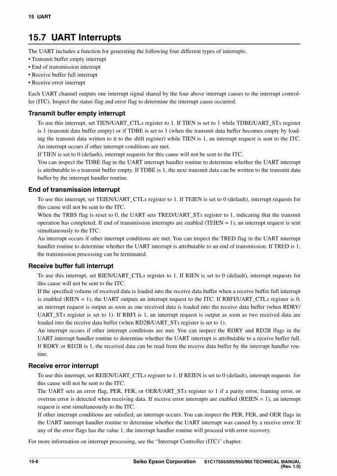
15 uaRT
15-8 Seiko epson Corporation S1C17555/565/955/965 TeChniCal Manual (Rev. 1.0)
uaRT interrupts15.7 The UART includes a function for generating the following four different types of interrupts.• Transmit buffer empty interrupt• End of transmission interrupt• Receive buffer full interrupt• Receive error interrupt
Each UART channel outputs one interrupt signal shared by the four above interrupt causes to the interrupt control-ler (ITC). Inspect the status flag and error flag to determine the interrupt cause occurred.
Transmit buffer empty interrupt To use this interrupt, set TIEN/UART_CTLx register to 1. If TIEN is set to 1 while TDBE/UART_STx register
is 1 (transmit data buffer empty) or if TDBE is set to 1 (when the transmit data buffer becomes empty by load-ing the transmit data written to it to the shift register) while TIEN is 1, an interrupt request is sent to the ITC. An interrupt occurs if other interrupt conditions are met.
If TIEN is set to 0 (default), interrupt requests for this cause will not be sent to the ITC. You can inspect the TDBE flag in the UART interrupt handler routine to determine whether the UART interrupt
is attributable to a transmit buffer empty. If TDBE is 1, the next transmit data can be written to the transmit data buffer by the interrupt handler routine.
end of transmission interrupt To use this interrupt, set TEIEN/UART_CTLx register to 1. If TEIEN is set to 0 (default), interrupt requests for
this cause will not be sent to the ITC. When the TRBS flag is reset to 0, the UART sets TRED/UART_STx register to 1, indicating that the transmit
operation has completed. If end of transmission interrupts are enabled (TEIEN = 1), an interrupt request is sent simultaneously to the ITC.
An interrupt occurs if other interrupt conditions are met. You can inspect the TRED flag in the UART interrupt handler routine to determine whether the UART interrupt is attributable to an end of transmission. If TRED is 1, the transmission processing can be terminated.
Receive buffer full interrupt To use this interrupt, set RIEN/UART_CTLx register to 1. If RIEN is set to 0 (default), interrupt requests for
this cause will not be sent to the ITC. If the specified volume of received data is loaded into the receive data buffer when a receive buffer full interrupt
is enabled (RIEN = 1), the UART outputs an interrupt request to the ITC. If RBFI/UART_CTLx register is 0, an interrupt request is output as soon as one received data is loaded into the receive data buffer (when RDRY/UART_STx register is set to 1). If RBFI is 1, an interrupt request is output as soon as two received data are loaded into the receive data buffer (when RD2B/UART_STx register is set to 1).
An interrupt occurs if other interrupt conditions are met. You can inspect the RDRY and RD2B flags in the UART interrupt handler routine to determine whether the UART interrupt is attributable to a receive buffer full. If RDRY or RD2B is 1, the received data can be read from the receive data buffer by the interrupt handler rou-tine.
Receive error interrupt To use this interrupt, set REIEN/UART_CTLx register to 1. If REIEN is set to 0 (default), interrupt requests for
this cause will not be sent to the ITC. The UART sets an error flag, PER, FER, or OER/UART_STx register to 1 if a parity error, framing error, or
overrun error is detected when receiving data. If receive error interrupts are enabled (REIEN = 1), an interrupt request is sent simultaneously to the ITC.
If other interrupt conditions are satisfied, an interrupt occurs. You can inspect the PER, FER, and OER flags in the UART interrupt handler routine to determine whether the UART interrupt was caused by a receive error. If any of the error flags has the value 1, the interrupt handler routine will proceed with error recovery.
For more information on interrupt processing, see the “Interrupt Controller (ITC)” chapter.

15 uaRT
S1C17555/565/955/965 TeChniCal Manual Seiko epson Corporation 15-9(Rev. 1.0)
irDa interface15.8 This UART module includes an RZI modulator/demodulator circuit enabling implementation of IrDA 1.0-compatible infrared communication function simply by adding basic external circuits.
The transmit data output from the UART transmit shift register is input to the modulator circuit and output from the SOUTx pin after the Low pulse has been modulated to a 3 × sclk16 cycle.
sclk16
Modulator input (shift register output)
Modulator output (SOUTx)
1 2 3 8 9 10 11 16
3 × sclk16
Modulator input (shift register output)
Modulator output (SOUTx)
S1 D0 D1 D2 D3 D4 D5 D6 D7 P S2 S3
(S1: Start bit, S2 & S3: Stop bits, P: Parity bit)
8.1 Transmission Signal WaveformFigure 15.
The received IrDA signal is input to the demodulator circuit and the Low pulse width is converted to 16 × sclk16 cycles before entry to the receive shift register. The demodulator circuit uses the pulse detection clock selected separately from the transfer clock to detect Low pulses input (when minimum pulse width = 1.41 µs/115,200 bps).
(S1: Start bit, S2 & S3: Stop bits, P: Parity bit)
sclk16
Demodulator input (SINx)
Demodulator output (shift register input)
1 2 3 4 16
16 × sclk162 × sclk16 or more
Demodulator input (SINx)
Demodulator output (shift register input) S1 D0 D1 D2 D3 D4 D5 D6 D7 P S2 S3
8.2 Receive Signal WaveformFigure 15.
irDa enable To use the IrDA interface function, set IRMD/UART_EXPx register to 1. This enables the RZI modulator/de-
modulator circuit.
note: This setting must be performed before setting other UART conditions.
Serial data transfer control Data transfer control in IrDA mode is identical to that for normal interfaces. For detailed information on data
format settings and data transfer and interrupt control methods, refer to the preceding sections.
Control Register Details15.9 9.1 List of UART RegistersTable 15.
address Register name Function0x4100 UART_ST0 UART Ch.0 Status Register Indicates transfer, buffer and error statuses.0x4101 UART_TXD0 UART Ch.0 Transmit Data Register Transmit data0x4102 UART_RXD0 UART Ch.0 Receive Data Register Receive data
0x4103 UART_MOD0 UART Ch.0 Mode Register Sets transfer data format.
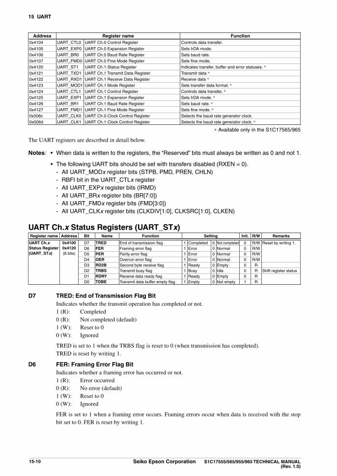
15 uaRT
15-10 Seiko epson Corporation S1C17555/565/955/965 TeChniCal Manual (Rev. 1.0)
address Register name Function0x4104 UART_CTL0 UART Ch.0 Control Register Controls data transfer.
0x4105 UART_EXP0 UART Ch.0 Expansion Register Sets IrDA mode.0x4106 UART_BR0 UART Ch.0 Baud Rate Register Sets baud rate.0x4107 UART_FMD0 UART Ch.0 Fine Mode Register Sets fine mode.0x4120 UART_ST1 UART Ch.1 Status Register Indicates transfer, buffer and error statuses. *0x4121 UART_TXD1 UART Ch.1 Transmit Data Register Transmit data *0x4122 UART_RXD1 UART Ch.1 Receive Data Register Receive data *0x4123 UART_MOD1 UART Ch.1 Mode Register Sets transfer data format. *0x4124 UART_CTL1 UART Ch.1 Control Register Controls data transfer. *0x4125 UART_EXP1 UART Ch.1 Expansion Register Sets IrDA mode. *0x4126 UART_BR1 UART Ch.1 Baud Rate Register Sets baud rate. *0x4127 UART_FMD1 UART Ch.1 Fine Mode Register Sets fine mode. *0x506c UART_CLK0 UART Ch.0 Clock Control Register Selects the baud rate generator clock. 0x506d UART_CLK1 UART Ch.1 Clock Control Register Selects the baud rate generator clock. *
* Available only in the S1C17565/965
The UART registers are described in detail below.
notes: • When data is written to the registers, the “Reserved” bits must always be written as 0 and not 1.
• The following UART bits should be set with transfers disabled (RXEN = 0).- All UART_MODx register bits (STPB, PMD, PREN, CHLN)- RBFI bit in the UART_CTLx register- All UART_EXPx register bits (IRMD)- All UART_BRx register bits (BR[7:0])- All UART_FMDx register bits (FMD[3:0])- All UART_CLKx register bits (CLKDIV[1:0], CLKSRC[1:0], CLKEN)
uaRT Ch.x Status Registers (uaRT_STx)Register name address Bit name Function Setting init. R/W Remarks
uaRT Ch.x Status Register(uaRT_STx)
0x41000x4120(8 bits)
D7 TReD End of transmission flag 1 Completed 0 Not completed 0 R/W Reset by writing 1.D6 FeR Framing error flag 1 Error 0 Normal 0 R/WD5 PeR Parity error flag 1 Error 0 Normal 0 R/WD4 OeR Overrun error flag 1 Error 0 Normal 0 R/WD3 RD2B Second byte receive flag 1 Ready 0 Empty 0 RD2 TRBS Transmit busy flag 1 Busy 0 Idle 0 R Shift register statusD1 RDRY Receive data ready flag 1 Ready 0 Empty 0 RD0 TDBe Transmit data buffer empty flag 1 Empty 0 Not empty 1 R
D7 TReD: end of Transmission Flag Bit Indicates whether the transmit operation has completed or not. 1 (R): Completed 0 (R): Not completed (default) 1 (W): Reset to 0 0 (W): Ignored
TRED is set to 1 when the TRBS flag is reset to 0 (when transmission has completed). TRED is reset by writing 1.
D6 FeR: Framing error Flag Bit Indicates whether a framing error has occurred or not. 1 (R): Error occurred 0 (R): No error (default) 1 (W): Reset to 0 0 (W): Ignored
FER is set to 1 when a framing error occurs. Framing errors occur when data is received with the stop bit set to 0. FER is reset by writing 1.
15 uaRT
S1C17555/565/955/965 TeChniCal Manual Seiko epson Corporation 15-11(Rev. 1.0)
D5 PeR: Parity error Flag Bit Indicates whether a parity error has occurred or not. 1 (R): Error occurred 0 (R): No error (default) 1 (W): Reset to 0 0 (W): Ignored
PER is set to 1 when a parity error occurs. Parity checking is enabled only when PREN/ UART_MODx register is set to 1 and is performed when received data is transferred from the shift register to the re-ceive data buffer. PER is reset by writing 1.
D4 OeR: Overrun error Flag Bit Indicates whether an overrun error has occurred or not. 1 (R): Error occurred 0 (R): No error (default) 1 (W): Reset to 0 0 (W): Ignored
OER is set to 1 when an overrun error occurs. Overrun errors occur when data is received in the shift register when the receive data buffer is already full and additional data is sent. The receive data buffer is not overwritten even if this error occurs. The shift register is overwritten as soon as the error occurs.
OER is reset by writing 1.
D3 RD2B: Second Byte Receive Flag Bit Indicates that the receive data buffer contains two received data. 1 (R): Second byte can be read 0 (R): Second byte not received (default)
RD2B is set to 1 when the second byte of data is loaded into the receive data buffer and is reset to 0 when the first data is read from the receive data buffer.
D2 TRBS: Transmit Busy Flag Bit Indicates the transmit shift register status. 1 (R): Operating 0 (R): Standby (default)
TRBS is set to 1 when transmit data is loaded from the transmit data buffer into the shift register and is reset to 0 when the data transfer is completed. Inspect TRBS to determine whether the transmit circuit is operating or at standby.
D1 RDRY: Receive Data Ready Flag Bit Indicates that the receive data buffer contains valid received data. 1 (R): Data can be read 0 (R): Buffer empty (default)
RDRY is set to 1 when received data is loaded into the receive data buffer and is reset to 0 when all data has been read from the receive data buffer.
D0 TDBe: Transmit Data Buffer empty Flag Bit Indicates the transmit data buffer status. 1 (R): Buffer empty (default) 0 (R): Data exists
TDBE is reset to 0 when transmit data is written to the transmit data buffer and is set to 1 when the data is transferred to the shift register.

15 uaRT
15-12 Seiko epson Corporation S1C17555/565/955/965 TeChniCal Manual (Rev. 1.0)
uaRT Ch.x Transmit Data Registers (uaRT_TXDx)Register name address Bit name Function Setting init. R/W Remarks
uaRT Ch.x Transmit Data Register(uaRT_TXDx)
0x41010x4121(8 bits)
D7–0 TXD[7:0] Transmit dataTXD7(6) = MSBTXD0 = LSB
0x0 to 0xff (0x7f) 0x0 R/W
D[7:0] TXD[7:0]: Transmit Data Write transmit data to be set in the transmit data buffer. (Default: 0x0) The UART starts transmitting when data is written to this register. Data written to TXD[7:0] is retained
until sent to the transmit data buffer. Transmitting data from within the transmit data buffer generates a cause of transmit buffer empty interrupt.
TXD7 (MSB) is invalid in 7-bit mode. Serial converted data is output from the SOUTx pin beginning with the LSB, in which the bits set to 1
are output as High level and bits set to 0 as Low level signals. This register can also be read.
uaRT Ch.x Receive Data Registers (uaRT_RXDx)Register name address Bit name Function Setting init. R/W Remarks
uaRT Ch.x Receive Data Register(uaRT_RXDx)
0x41020x4122(8 bits)
D7–0 RXD[7:0] Receive data in the receive data bufferRXD7(6) = MSBRXD0 = LSB
0x0 to 0xff (0x7f) 0x0 R Older data in the buf-fer is read out first.
D[7:0] RXD[7:0]: Receive Data Data in the receive data buffer is read out in sequence, starting with the oldest. Received data is placed in
the receive data buffer. The receive data buffer is a 2-byte FIFO that allows proper data reception until it fills, even if data is not read out. If the buffer is full and the shift register also contains received data, an overrun error will occur, unless the data is read out before reception of the subsequent data starts.
The receive circuit includes two receive buffer status flags: RDRY/UART_STx register and RD2B/UART_STx register. The RDRY flag indicates the presence of valid received data in the receive data buffer, while the RD2B flag indicates the presence of two received data in the receive data buffer.
A receive buffer full interrupt occurs when the received data in the receive data buffer reaches the num-ber specified by RBFI/UART_CTLx register.
0 is loaded into RXD7 in 7-bit mode. Serial data input via the SINx pin is converted to parallel, with the initial bit as LSB, the High level bit
as 1, and the Low level bit as 0. This data is then loaded into the receive data buffer. This register is read-only. (Default: 0x0)
uaRT Ch.x Mode Registers (uaRT_MODx)Register name address Bit name Function Setting init. R/W Remarks
uaRT Ch.x Mode Register(uaRT_MODx)
0x41030x4123(8 bits)
D7–5 – reserved – – – 0 when being read.D4 Chln Character length select 1 8 bits 0 7 bits 0 R/WD3 PRen Parity enable 1 With parity 0 No parity 0 R/WD2 PMD Parity mode select 1 Odd 0 Even 0 R/WD1 STPB Stop bit select 1 2 bits 0 1 bit 0 R/WD0 – reserved – – – 0 when being read.
D[7:5] Reserved
D4 Chln: Character length Select Bit Selects the serial transfer data length. 1 (R/W): 8 bits 0 (R/W): 7 bits (default)
D3 PRen: Parity enable Bit Enables the parity function. 1 (R/W): With parity 0 (R/W): No parity (default)

15 uaRT
S1C17555/565/955/965 TeChniCal Manual Seiko epson Corporation 15-13(Rev. 1.0)
PREN is used to select whether received data parity checking is performed and whether a parity bit is added to transmit data. Setting PREN to 1 parity-checks the received data. A parity bit is automatically added to the transmit data. If PREN is set to 0, no parity bit is checked or added.
D2 PMD: Parity Mode Select Bit Selects the parity mode. 1 (R/W): Odd parity 0 (R/W): Even parity (default)
Writing 1 to PMD selects odd parity; writing 0 to it selects even parity. Parity checking and parity bit addition are enabled only when PREN is set to 1. The PMD setting is disabled if PREN is 0.
D1 STPB: Stop Bit Select Bit Selects the stop bit length. 1 (R/W): 2 bits 0 (R/W): 1 bit (default)
Writing 1 to STPB selects 2 stop bits; writing 0 to it selects 1 bit. The start bit is fixed at 1 bit.
D0 Reserved
uaRT Ch.x Control Registers (uaRT_CTlx)Register name address Bit name Function Setting init. R/W Remarks
uaRT Ch.x Control Register(uaRT_CTlx)
0x41040x4124(8 bits)
D7 Teien End of transmission int. enable 1 Enable 0 Disable 0 R/WD6 Reien Receive error int. enable 1 Enable 0 Disable 0 R/WD5 Rien Receive buffer full int. enable 1 Enable 0 Disable 0 R/WD4 Tien Transmit buffer empty int. enable 1 Enable 0 Disable 0 R/W
D3–2 – reserved – – – 0 when being read.D1 RBFi Receive buffer full int. condition setup 1 2 bytes 0 1 byte 0 R/WD0 RXen UART enable 1 Enable 0 Disable 0 R/W
D7 Teien: end of Transmission interrupt enable Bit Enables interrupt requests to the ITC when transmit operation has completed. 1 (R/W): Enabled 0 (R/W): Disabled (default)
Set this bit to 1 to terminate transmit processing using interrupts.
D6 Reien: Receive error interrupt enable Bit Enables interrupt requests to the ITC when a receive error occurs. 1 (R/W): Enabled 0 (R/W): Disabled (default)
Set this bit to 1 to process receive errors using interrupts.
D5 Rien: Receive Buffer Full interrupt enable Bit Enables interrupt requests to the ITC caused when the received data quantity in the receive data buffer
reaches the quantity specified in RBFI. 1 (R/W): Enabled 0 (R/W): Disabled (default)
Set this bit to 1 to read received data using interrupts.
D4 Tien: Transmit Buffer empty interrupt enable Bit Enables interrupt requests to the ITC caused when transmission data in the transmit data buffer is sent
to the shift register (i.e. when data transmission begins). 1 (R/W): Enabled 0 (R/W): Disabled (default)
Set this bit to 1 to write data to the transmit data buffer using interrupts.
D[3:2] Reserved

15 uaRT
15-14 Seiko epson Corporation S1C17555/565/955/965 TeChniCal Manual (Rev. 1.0)
D1 RBFi: Receive Buffer Full interrupt Condition Setup Bit Sets the quantity of data in the receive data buffer to generate a receive buffer full interrupt. 1 (R/W): 2 bytes 0 (R/W): 1 byte (default)
If receive buffer full interrupts are enabled (RIEN = 1), the UART outputs an interrupt request to the ITC when the quantity of received data specified by RBFI is loaded into the receive data buffer.
If RBFI is 0, an interrupt request is output as soon as one received data is loaded into the receive data buffer (when RDRY/UART_STx register is set to 1). If RBFI is 1, an interrupt request is output as soon as two received data are loaded into the receive data buffer (when RD2B/UART_STx register is set to 1).
D0 RXen: uaRT enable Bit Enables data transfer by the UART. 1 (R/W): Enabled 0 (R/W): Disabled (default)
Set RXEN to 1 before starting UART transfers. Setting RXEN to 0 disables data transfers. The data being transferred cannot be guaranteed if RXEN
is set to 0 while data is being sent or received. Before setting RXEN to 0, check the data transfer sta-tus with software in consideration of the communication procedure. The data transmit status can be checked using the TRBS flag.
The transfer conditions must be set while RXEN is 0. Disabling transfers by writing 0 to RXEN also clears transmit data buffer.
uaRT Ch.x expansion Registers (uaRT_eXPx)Register name address Bit name Function Setting init. R/W Remarks
uaRT Ch.xexpansion Register(uaRT_eXPx)
0x41050x4125(8 bits)
D7–1 – reserved – – – 0 when being read.
D0 iRMD IrDA mode select 1 On 0 Off 0 R/W
D[7:1] Reserved
D0 iRMD: irDa Mode Select Bit Switches the IrDA interface function on and off. 1 (R/W): On 0 (R/W): Off (default)
Set IRMD to 1 to use the IrDA interface. When IRMD is set to 0, this module functions as a normal UART, with no IrDA functions.
uaRT Ch.x Baud Rate Registers (uaRT_BRx)Register name address Bit name Function Setting init. R/W Remarks
uaRT Ch.xBaud Rate Register(uaRT_BRx)
0x41060x4126(8 bits)
D7–0 BR[7:0] Baud rate setting 0x0 to 0xff 0x0 R/W
D[7:0] BR[7:0]: Baud Rate Setting Bits Sets the initial counter value of the baud rate generator. (Default: 0x0) The counter in the baud rate generator repeats counting from the value set in this register to occurrence
of counter underflow to generate the transfer (sampling) clock. Use the following equations to calculate the initial counter value for obtaining the desired transfer rate.
ct_clkbps = —————————— {(BR + 1) × 16 + FMD} ct_clkBR = (——— - FMD - 16) ÷ 16 bps
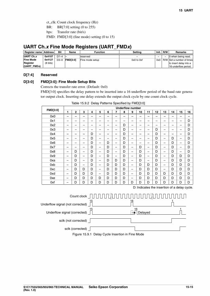
15 uaRT
S1C17555/565/955/965 TeChniCal Manual Seiko epson Corporation 15-15(Rev. 1.0)
ct_clk: Count clock frequency (Hz)BR: BR[7:0] setting (0 to 255)bps: Transfer rate (bit/s)FMD: FMD[3:0] (fine mode) setting (0 to 15)
uaRT Ch.x Fine Mode Registers (uaRT_FMDx)Register name address Bit name Function Setting init. R/W Remarks
uaRT Ch.x Fine Mode Register(uaRT_FMDx)
0x41070x4127(8 bits)
D7–4 – reserved – – – 0 when being read.D3–0 FMD[3:0] Fine mode setup 0x0 to 0xf 0x0 R/W Set a number of times
to insert delay into a 16-underflow period.
D[7:4] Reserved
D[3:0] FMD[3:0]: Fine Mode Setup Bits Corrects the transfer rate error. (Default: 0x0) FMD[3:0] specifies the delay pattern to be inserted into a 16 underflow period of the baud rate genera-
tor output clock. Inserting one delay extends the output clock cycle by one count clock cycle.
9.2 Delay Patterns Specified by FMD[3:0]Table 15.
FMD[3:0]underflow number
1 2 3 4 5 6 7 8 9 10 11 12 13 14 15 16
0x0 – – – – – – – – – – – – – – – –0x1 – – – – – – – – – – – – – – – D0x2 – – – – – – – D – – – – – – – D0x3 – – – – – – – D – – – D – – – D0x4 – – – D – – – D – – – D – – – D0x5 – – – D – – – D – – – D – D – D0x6 – – – D – D – D – – – D – D – D0x7 – – – D – D – D – D – D – D – D0x8 – D – D – D – D – D – D – D – D0x9 – D – D – D – D – D – D – D D D0xa – D – D – D D D – D – D – D D D0xb – D – D – D D D – D D D – D D D0xc – D D D – D D D – D D D – D D D0xd – D D D – D D D – D D D D D D D0xe – D D D D D D D – D D D D D D D0xf – D D D D D D D D D D D D D D D
D: Indicates the insertion of a delay cycle.
Count clock
Underflow signal (not corrected)
Underflow signal (corrected)
sclk (not corrected)
sclk (corrected)
Delayed
15 16
15 16
1
1
9.1 Delay Cycle Insertion in Fine ModeFigure 15.

15 uaRT
15-16 Seiko epson Corporation S1C17555/565/955/965 TeChniCal Manual (Rev. 1.0)
uaRT Ch.x Clock Control Registers (uaRT_ClKx)Register name address Bit name Function Setting init. R/W Remarks
uaRT Ch.x Clock Control Register(uaRT_ClKx)
0x506c0x506d(8 bits)
D7–6 – reserved – – – 0 when being read.D5–4 ClKDiV
[1:0]Clock division ratio select CLKDIV[1:0] Division ratio 0x0 R/W When the clock
source is IOSC or OSC3
0x30x20x10x0
1/81/41/21/1
D3–2 ClKSRC[1:0]
Clock source select CLKSRC[1:0] Clock source 0x0 R/W * S1C17565/965 only0x3
0x20x10x0
External clockOSC3*OSC1IOSC
D1 – reserved – – – 0 when being read.D0 ClKen Count clock enable 1 Enable 0 Disable 0 R/W
D[7:6] Reserved
D[5:4] ClKDiV[1:0]: Clock Division Ratio Select Bits Selects the division ratio for generating the count clock of the baud rate generator when IOSC or OSC3
is used as the clock source.
9.3 IOSC/OSC3 Division Ratio SelectionTable 15.
ClKDiV[1:0] Division ratio
0x3 1/80x2 1/40x1 1/20x0 1/1
(Default: 0x0)
D[3:2] ClKSRC[1:0]: Clock Source Select Bits Selects the count clock source for the baud rate generator.
9.4 Clock Source SelectionTable 15.
ClKSRC[1:0]Clock source
S1C17555/955 S1C17565/965
0x3 Reserved0x2 Reserved OSC30x1 OSC1 OSC10x0 IOSC IOSC
(Default: 0x0)
D1 Reserved
D0 ClKen: Count Clock enable Bit Enables or disables the count clock supply to the counter of the baud rate generator. 1 (R/W): Enabled (on) 0 (R/W): Disabled (off) (default)
The CLKEN default setting is 0, which disables the clock supply. Setting CLKEN to 1 sends the clock selected to the counter.

16 8-bit SPi (SPi)
S1C17555/565/955/965 TeChniCal Manual Seiko epson Corporation 16-1(Rev. 1.0)
8-bit SPI (SPI)16
SPi Module Overview16.1 The S1C17555/565/955/965 includes an 8-bit‚ synchronized serial interface module (SPI) with two communication channels. The following shows the main features of the SPI:
• Supports both master and slave modes. (Multi-slave mode is not supported.)
• Data length: 8 bits fixed
• Supports both MSB first and LSB first modes.
• Contains one-byte receive data buffer and one-byte transmit data buffer.
• Supports full-duplex communications.
• Data transfer timing (clock phase and polarity variations) is selectable from among 4 types.
• Can generate receive buffer full and transmit buffer empty interrupts.
Figure 16.1.1 shows the SPI module configuration.
Shift registerReceive data buffer (1 byte)
SDIx
PCLK
Internal bus
ITC
SPI Ch.x
Bus I/Fand
controlregisters
SPICLKx#SPISSx
Shift registerTransmit data buffer (1 byte)
Clock/transfer control
SDOx
T16 Ch.1output clock
Interruptcontrol
1/4
1.1 SPI Module Configuration (1 channel)Figure 16.
note: Two channels in the SPI module have the same functions except for control register addresses. For this reason, the description in this chapter applies to all SPI channels. The ‘x’ in the register name indicates the channel number (0 or 1).
Example: SPI_CTLx register Ch.0: SPI_CTL0 register Ch.1: SPI_CTL1 register
SPi input/Output Pins16.2 Table 16.2.1 lists the SPI pins.
2.1 List of SPI PinsTable 16.
Pin name i/O Qty Function
SDI0 (Ch.0)SDI1 (Ch.1)
I 2 SPI Ch.x data input pinInputs serial data from SPI bus.
SDO0 (Ch.0)SDO1 (Ch.1)
O 2 SPI Ch.x data output pinOutputs serial data to SPI bus.
SPICLK0 (Ch.0)SPICLK1 (Ch.1)
I/O 2 SPI Ch.x external clock input/output pinOutputs SPI clock when SPI is in master mode.Inputs external clock when SPI is used in slave mode.

16 8-bit SPi (SPi)
16-2 Seiko epson Corporation S1C17555/565/955/965 TeChniCal Manual (Rev. 1.0)
Pin name i/O Qty Function
#SPISS0 (Ch.0)#SPISS1 (Ch.1)
I 2 SPI Ch.x slave select signal (active Low) input pinSPI (Slave mode) is selected as a slave device by Low input to this pin.
note: Use an I/O (P) port to output the slave select signal when the SPI module is configured to master mode.
The SPI input/output pins (SDIx, SDOx, SPICLKx, #SPISSx) are shared with I/O ports and are initially set as gen-eral purpose I/O port pins. The pin functions must be switched using the port function select bits to use the general purpose I/O port pins as SPI input/output pins.For detailed information on pin function switching, see the “I/O Ports (P)” chapter.
SPi Clock16.3 The master mode SPI uses the 16-bit timer (T16) Ch.1 output clock or a PCLK/4 clock to generate the SPI clock. This clock is output from the SPICLKx pin to the slave device while also driving the shift register.Use MCLK/SPI_CTLx register to select whether the T16 Ch.1 output clock or PCLK/4 clock is used.Setting MCLK to 1 selects the T16 Ch.1 output clock; setting to 0 selects the PCLK/4 clock.Using the T16 Ch.1 output clock enables programmable transfer rates. For more information on T16 control, see the “16-bit Timers (T16)” chapter.
PCLK
16-bit timer Ch.1 output clockor
PCLK/4
SPI clock (SPICLKx output)
3.1 Master Mode SPI ClockFigure 16.
In slave mode, the SPI clock is input via the SPICLKx pin.
Data Transfer Condition Settings16.4 The SPI module can be set to master or slave modes. The SPI clock polarity/phase and bit direction (MSB first/LSB first) can also be set via the SPI_CTLx register. The data length is fixed at 8 bits.
note: Make sure the SPI module is halted (SPEN/SPI_CTLx register = 0) before master/slave mode se-lection and clock condition settings.
Master/slave mode selection MSSL/SPI_CTLx register is used to set the SPI module to master mode or slave mode. Setting MSSL to 1 sets
master mode; setting it to 0 (default) sets slave mode. In master mode, data is transferred using the internal clock. In slave mode, data is transferred by inputting the master device clock.
SPi clock polarity and phase settings The SPI clock polarity is selected by CPOL/SPI_CTLx register. Setting CPOL to 1 treats the SPI clock as ac-
tive Low; setting it to 0 (default) treats it as active High. The SPI clock phase is selected by CPHA/SPI_CTLx register.
As shown below, these control bits set transfer timing.
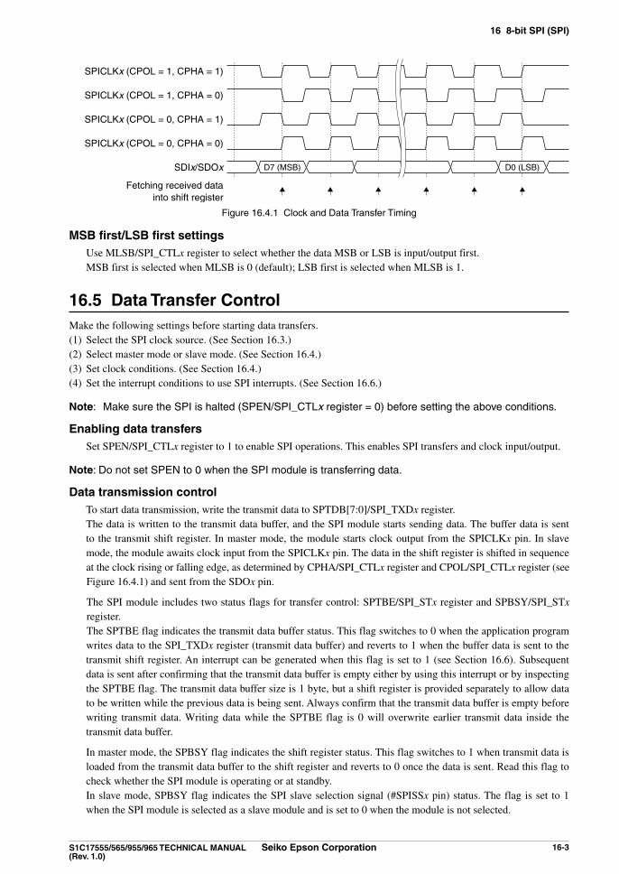
16 8-bit SPi (SPi)
S1C17555/565/955/965 TeChniCal Manual Seiko epson Corporation 16-3(Rev. 1.0)
SPICLKx (CPOL = 1, CPHA = 1)
SPICLKx (CPOL = 1, CPHA = 0)
SPICLKx (CPOL = 0, CPHA = 1)
SPICLKx (CPOL = 0, CPHA = 0)
SDIx/SDOx
Fetching received datainto shift register
D7 (MSB) D0 (LSB)
4.1 Clock and Data Transfer TimingFigure 16.
MSB first/lSB first settings Use MLSB/SPI_CTLx register to select whether the data MSB or LSB is input/output first. MSB first is selected when MLSB is 0 (default); LSB first is selected when MLSB is 1.
Data Transfer Control16.5 Make the following settings before starting data transfers.(1) Select the SPI clock source. (See Section 16.3.)(2) Select master mode or slave mode. (See Section 16.4.)(3) Set clock conditions. (See Section 16.4.)(4) Set the interrupt conditions to use SPI interrupts. (See Section 16.6.)
note: Make sure the SPI is halted (SPEN/SPI_CTLx register = 0) before setting the above conditions.
enabling data transfers Set SPEN/SPI_CTLx register to 1 to enable SPI operations. This enables SPI transfers and clock input/output.
note: Do not set SPEN to 0 when the SPI module is transferring data.
Data transmission control To start data transmission, write the transmit data to SPTDB[7:0]/SPI_TXDx register. The data is written to the transmit data buffer, and the SPI module starts sending data. The buffer data is sent
to the transmit shift register. In master mode, the module starts clock output from the SPICLKx pin. In slave mode, the module awaits clock input from the SPICLKx pin. The data in the shift register is shifted in sequence at the clock rising or falling edge, as determined by CPHA/SPI_CTLx register and CPOL/SPI_CTLx register (see Figure 16.4.1) and sent from the SDOx pin.
The SPI module includes two status flags for transfer control: SPTBE/SPI_STx register and SPBSY/SPI_STx register.
The SPTBE flag indicates the transmit data buffer status. This flag switches to 0 when the application program writes data to the SPI_TXDx register (transmit data buffer) and reverts to 1 when the buffer data is sent to the transmit shift register. An interrupt can be generated when this flag is set to 1 (see Section 16.6). Subsequent data is sent after confirming that the transmit data buffer is empty either by using this interrupt or by inspecting the SPTBE flag. The transmit data buffer size is 1 byte, but a shift register is provided separately to allow data to be written while the previous data is being sent. Always confirm that the transmit data buffer is empty before writing transmit data. Writing data while the SPTBE flag is 0 will overwrite earlier transmit data inside the transmit data buffer.
In master mode, the SPBSY flag indicates the shift register status. This flag switches to 1 when transmit data is loaded from the transmit data buffer to the shift register and reverts to 0 once the data is sent. Read this flag to check whether the SPI module is operating or at standby.
In slave mode, SPBSY flag indicates the SPI slave selection signal (#SPISSx pin) status. The flag is set to 1 when the SPI module is selected as a slave module and is set to 0 when the module is not selected.

16 8-bit SPi (SPi)
16-4 Seiko epson Corporation S1C17555/565/955/965 TeChniCal Manual (Rev. 1.0)
note: When the SPI module is used in master mode with CPHA set to 0, the clock may change a mini-mum of one system clock (PCLK) cycle time from change of the first transmit data bit.
PCLK
16-bit timer output
SPI_TXDx register
SPICLKx
SDOx
Write
Minimum 1/fPCLK
5.1 SDOFigure 16. x and SPICLKx Change Timings when CPHA = 0
The half SPICLKx cycle will be secured from change of data to change of the clock for the second and following transmit data bits and the second and following bytes during continuous transfer.
Data reception control In master mode, write dummy data to SPTDB[7:0]/SPI_TXDx register. Writing to the SPI_TXDx register cre-
ates the trigger for reception as well as transmission start. Writing actual transmit data enables simultaneous transmission and reception.
This starts the SPI clock output from the SPICLKx pin.
In slave mode, the module waits until the clock is input from the SPICLKx pin. There is no need to write to the SPI_TXDx register if no transmission is required. The receiving operation is started by the clock input from the master device. If data is transmitted simultaneously, write transmit data to the SPI_TXDx register before the clock is input.
The data is received in sequence in the shift register at the rising or falling edge of the clock determined by CPHA/SPI_CTLx register and CPOL/SPI_CTLx register. (See Figure 16.4.1.) The received data is loaded into the receive data buffer once the 8 bits of data are received in the shift register.
The received data in the buffer can be read from SPRDB[7:0]/SPI_RXDx register.
The SPI module includes SPRBF/SPI_STx register for reception control. The SPRBF flag indicates the receive data buffer status. This flag is set to 1 when the data received in the shift
register is loaded into the receive data buffer, indicating that the received data can be read out. It reverts to 0 when the buffer data is read out from the SPI_RXDx register. An interrupt can be generated as soon as the flag is set to 1 (see Section 16.6). The received data should be read out either by using this interrupt or by inspecting the SPRBF flag to confirm that the receive data buffer contains valid received data. The receive data buffer is 1 byte in size, but a shift register is also provided, enabling received data to be retained in the buffer even while the subsequent data is being received. Note that the receive data buffer should be read out before receiving the subsequent data is complete. If receiving the subsequent data is complete before the receive data buffer contents are read out, the newly received data will overwrite the previous received data in the buffer.
In master mode, the SPBSY flag indicating the shift register status can be used in the same way while transfer-ring data.

16 8-bit SPi (SPi)
S1C17555/565/955/965 TeChniCal Manual Seiko epson Corporation 16-5(Rev. 1.0)
PCLK
SPEN
SPI_TXDx register
Shift register
SPICLKx pin(CPOL = 0, CPHA = 1)
SPICLKx pin(CPOL = 0, CPHA = 0)
SDOx pin
SDIx pin
SPI_RXDx register
SPBSY
SPTBE
SPRBF
AD7 AD6 AD5 AD4 AD3 AD0
Data A Data B Data C
Data A' Data B'
Write Write Write
Read Read
AD1AD2 BD7 BD6 BD5 BD4 BD3 BD0BD1BD2
A'D7 A'D6 A'D5 A'D4 A'D3 A'D0A'D1A'D2 B'D7 B'D6 B'D5 B'D4 B'D3 B'D0B'D1B'D2
5.2 Data Transmission/Receiving Timing Chart (MSB first)Figure 16.
Disabling data transfers After a data transfer is completed (both transmission and reception), write 0 to SPEN to disable data transfers.
Confirm that the SPTBE flag is 1 and the SPBSY flag is 0 before disabling data transfer. The data being transferred cannot be guaranteed if SPEN is set to 0 while data is being sent or received.
SPi interrupts16.6 Each channel of the SPI module includes a function for generating the following two different types of interrupts.• Transmit buffer empty interrupt• Receive buffer full interrupt
The SPI channel outputs one interrupt signal shared by the two above interrupt causes to the interrupt controller (ITC). Inspect the status flag to determine the interrupt cause occurred.
Transmit buffer empty interrupt To use this interrupt, set SPTIE/SPI_CTLx register to 1. If SPTIE is set to 0 (default), interrupt requests for this
cause will not be sent to the ITC. When transmit data written to the transmit data buffer is transferred to the shift register, the SPI module sets
SPTBE/SPI_STx register to 1, indicating that the transmit data buffer is empty. If transmit buffer empty inter-rupts are enabled (SPTIE = 1), an interrupt request is sent simultaneously to the ITC.
An interrupt occurs if other interrupt conditions are met. You can inspect the SPTBE flag in the SPI interrupt handler routine to determine whether the SPI interrupt is attributable to a transmit buffer empty. If SPTBE is 1, the next transmit data can be written to the transmit data buffer by the interrupt handler routine.
Receive buffer full interrupt To use this interrupt, set SPRIE/SPI_CTLx register to 1. If SPRIE is set to 0 (default), interrupt requests for this
cause will not be sent to the ITC. When data received in the shift register is loaded into the receive data buffer, the SPI module sets SPRBF/SPI_
STx register to 1, indicating that the receive data buffer contains readable received data. If receive buffer full interrupts are enabled (SPRIE = 1), an interrupt request is output to the ITC at the same time.
An interrupt occurs if other interrupt conditions are met. You can inspect the SPRBF flag in the SPI interrupt handler routine to determine whether the SPI interrupt is attributable to a receive buffer full. If SPRBF is 1, the received data can be read from the receive data buffer by the interrupt handler routine.
For more information on interrupt processing, see the “Interrupt Controller (ITC)” chapter.

16 8-bit SPi (SPi)
16-6 Seiko epson Corporation S1C17555/565/955/965 TeChniCal Manual (Rev. 1.0)
Control Register Details16.7
7.1 List of SPI RegistersTable 16.
address Register name Function0x4320 SPI_ST0 SPI Ch.0 Status Register Indicates transfer and buffer statuses.0x4322 SPI_TXD0 SPI Ch.0 Transmit Data Register Transmit data0x4324 SPI_RXD0 SPI Ch.0 Receive Data Register Receive data
0x4326 SPI_CTL0 SPI Ch.0 Control Register Sets the SPI mode and enables data transfer.0x4380 SPI_ST1 SPI Ch.1 Status Register Indicates transfer and buffer statuses.0x4382 SPI_TXD1 SPI Ch.1 Transmit Data Register Transmit data0x4384 SPI_RXD1 SPI Ch.1 Receive Data Register Receive data0x4386 SPI_CTL1 SPI Ch.1 Control Register Sets the SPI mode and enables data transfer.
The SPI registers are described in detail below.
note: When data is written to the registers, the “Reserved” bits must always be written as 0 and not 1.
SPi Ch.x Status Registers (SPi_STx)Register name address Bit name Function Setting init. R/W Remarks
SPi Ch.x Status Register(SPi_STx)
0x43200x4380(16 bits)
D15–3 – reserved – – – 0 when being read.D2 SPBSY Transfer busy flag (master) 1 Busy 0 Idle 0 R
ss signal low flag (slave) 1 ss = L 0 ss = HD1 SPRBF Receive data buffer full flag 1 Full 0 Not full 0 RD0 SPTBe Transmit data buffer empty flag 1 Empty 0 Not empty 1 R
D[15:3] Reserved
D2 SPBSY: Transfer Busy Flag Bit (Master Mode)/ss Signal low Flag Bit (Slave Mode)
Master mode Indicates the SPI transfer status. 1 (R): Operating 0 (R): Standby (default)
SPBSY is set to 1 when the SPI starts data transfer in master mode and is maintained at 1 while transfer is underway. It is cleared to 0 once the transfer is complete.
Slave mode Indicates the slave selection (#SPISSx) signal status. 1 (R): Low level (this SPI is selected) 0 (R): High level (this SPI is not selected) (default)
SPBSY is set to 1 when the master device asserts the #SPISSx signal to select this SPI module (slave device). It is returned to 0 when the master device clears the SPI module selection by negating the #SPISSx signal.
D1 SPRBF: Receive Data Buffer Full Flag Bit Indicates the receive data buffer status. 1 (R): Data full 0 (R): No data (default)
SPRBF is set to 1 when data received in the shift register is sent to the receive data buffer (when receiv-ing is completed), indicating that the data can be read. It reverts to 0 once the buffer data is read from the SPI_RXDx register.

16 8-bit SPi (SPi)
S1C17555/565/955/965 TeChniCal Manual Seiko epson Corporation 16-7(Rev. 1.0)
D0 SPTBe: Transmit Data Buffer empty Flag Bit Indicates the transmit data buffer status. 1 (R): Empty (default) 0 (R): Data exists
SPTBE is set to 0 when transmit data is written to the SPI_TXDx register (transmit data buffer), and is set to 1 when the data is transferred to the shift register (when transmission starts).
Transmission data must be written to the SPI_TXDx register when this bit is 1.
SPi Ch.x Transmit Data Registers (SPi_TXDx)Register name address Bit name Function Setting init. R/W Remarks
SPi Ch.x Transmit Data Register(SPi_TXDx)
0x43220x4382(16 bits)
D15–8 – reserved – – – 0 when being read.D7–0 SPTDB[7:0] SPI transmit data buffer
SPTDB7 = MSBSPTDB0 = LSB
0x0 to 0xff 0x0 R/W
D[15:8] Reserved
D[7:0] SPTDB[7:0]: SPi Transmit Data Buffer Bits Sets transmit data to be written to the transmit data buffer. (Default: 0x0) In master mode, transmission is started by writing data to this register. In slave mode, the contents of this
register are sent to the shift register and transmission begins when the clock is input from the master. SPTBE/SPI_STx register is set to 1 (empty) as soon as data written to this register has been transferred
to the shift register. A transmit buffer empty interrupt is generated at the same time. The subsequent transmit data can then be written, even while data is being transmitted.
Serial converted data is output from the SDOx pin, with the bit set to 1 as High level and the bit set to 0 as Low level.
note: Make sure that SPEN is set to 1 before writing data to the SPI_TXDx register to start data trans-mission/reception.
SPi Ch.x Receive Data Registers (SPi_RXDx)Register name address Bit name Function Setting init. R/W Remarks
SPi Ch.x Receive Data Register(SPi_RXDx)
0x43240x4384(16 bits)
D15–8 – reserved – – – 0 when being read.D7–0 SPRDB[7:0] SPI receive data buffer
SPRDB7 = MSBSPRDB0 = LSB
0x0 to 0xff 0x0 R
D[15:8] Reserved
D[7:0] SPRDB[7:0]: SPi Receive Data Buffer Bits Contains the received data. (Default: 0x0) SPRBF/SPI_STx register is set to 1 (data full) as soon as data is received and the shift register data has
been transferred to the receive data buffer. A receive buffer full interrupt is generated at the same time. Data can then be read until subsequent data is received. If receiving the subsequent data is completed before the register has been read out, the new received data overwrites the contents.
Serial data input from the SDIx pin is converted to parallel, with the High level bit set to 1 and the Low level bit set to 0. The data is the loaded into this register.
This register is read-only.
SPi Ch.x Control Registers (SPi_CTlx)Register name address Bit name Function Setting init. R/W Remarks
SPi Ch.x Con-trol Register(SPi_CTlx)
0x43260x4386(16 bits)
D15–10 – reserved – – – 0 when being read.D9 MClK SPI clock source select 1 T16 Ch.1 0 PCLK/4 0 R/WD8 MlSB LSB/MSB first mode select 1 LSB 0 MSB 0 R/W
D7–6 – reserved – – – 0 when being read.D5 SPRie Receive data buffer full int. enable 1 Enable 0 Disable 0 R/WD4 SPTie Transmit data buffer empty int. enable 1 Enable 0 Disable 0 R/WD3 CPha Clock phase select 1 Data out 0 Data in 0 R/W These bits must be
set before setting SPEN to 1.
D2 CPOl Clock polarity select 1 Active L 0 Active H 0 R/WD1 MSSl Master/slave mode select 1 Master 0 Slave 0 R/WD0 SPen SPI enable 1 Enable 0 Disable 0 R/W

16 8-bit SPi (SPi)
16-8 Seiko epson Corporation S1C17555/565/955/965 TeChniCal Manual (Rev. 1.0)
note: Do not access to the SPI_CTLx register while SPBSY/SPI_STx register is set to 1 or SPRBF/SPI_STx register is set to 1 (while data is being transmitted/received).
D[15:10] Reserved
D9 MClK: SPi Clock Source Select Bit Selects the SPI clock source. 1 (R/W): 16-bit timer Ch.1 0 (R/W): PCLK/4 (default)
D8 MlSB: lSB/MSB First Mode Select Bit Selects whether data is transferred with MSB first or LSB first. 1 (R/W): LSB first 0 (R/W): MSB first (default)
D[7:6] Reserved
D5 SPRie: Receive Data Buffer Full interrupt enable Bit Enables or disables SPI receive data buffer full interrupts. 1 (R/W): Enabled 0 (R/W): Disabled (default)
Setting SPRIE to 1 enables the output of SPI interrupt requests to the ITC due to a receive data buffer full. These interrupt requests are generated when the data received in the shift register is transferred to the receive data buffer (when reception is completed).
SPI interrupts are not generated by receive data buffer full if SPRIE is set to 0.
D4 SPTie: Transmit Data Buffer empty interrupt enable Bit Enables or disables SPI transmit data buffer empty interrupts. 1 (R/W): Enabled 0 (R/W): Disabled (default)
Setting SPTIE to 1 enables the output of SPI interrupt requests to the ITC due to a transmit data buffer empty. These interrupt requests are generated when the data written to the transmit data buffer is trans-ferred to the shift register (when transmission starts).
SPI interrupts are not generated by transmit data buffer empty if SPTIE is set to 0.
D3 CPha: Clock Phase Select Bit Selects the SPI clock phase. (Default: 0) Set the data transfer timing together with CPOL. (See Figure 16.7.1.)
D2 CPOl: Clock Polarity Select Bit Selects the SPI clock polarity. 1 (R/W): Active Low 0 (R/W): Active High (default)
Set the data transfer timing together with CPHA. (See Figure 16.7.1.)
SPICLKx (CPOL = 1, CPHA = 1)
SPICLKx (CPOL = 1, CPHA = 0)
SPICLKx (CPOL = 0, CPHA = 1)
SPICLKx (CPOL = 0, CPHA = 0)
SDIx/SDOx
Fetching received datainto shift register
D7 (MSB) D0 (LSB)
7.1 Clock and Data Transfer TimingFigure 16.
16 8-bit SPi (SPi)
S1C17555/565/955/965 TeChniCal Manual Seiko epson Corporation 16-9(Rev. 1.0)
D1 MSSl: Master/Slave Mode Select Bit Sets the SPI module to master or slave mode. 1 (R/W): Master mode 0 (R/W): Slave mode (default)
Setting MSSL to 1 selects master mode; setting it to 0 selects slave mode. Master mode performs data transfer with the internal clock. In slave mode, data is transferred by inputting the clock from the master device.
D0 SPen: SPi enable Bit Enables or disables SPI module operation. 1 (R/W): Enabled 0 (R/W): Disabled (default)
Setting SPEN to 1 starts the SPI module operation, enabling data transfer. Setting SPEN to 0 stops the SPI module operation.
note: The SPEN bit should be set to 0 before setting the CPHA, CPOL, and MSSL bits.

17 16-bit SPi (SPi16)
S1C17555/565/955/965 TeChniCal Manual Seiko epson Corporation 17-1(Rev. 1.0)
16-bit SPI (SPI16)17
SPi16 Module Overview17.1 The S1C17555/565/955/965 includes a synchronized serial interface module (SPI16) that supports a maximum 16 bits of data length. The following shows the main features of SPI16:
• Supports both master and slave modes. (Multi-slave mode is not supported.)
• Data length: 1 to 16 bits variable
• Fixed at MSB first data transfer.
• Contains two-byte receive data buffer and two-byte transmit data buffer.
• Supports full-duplex communications.
• Data transfer timing (clock phase and polarity variations) is selectable from among 4 types.
• Configurable delay time (wait time) between transfer data within the range from 0 to 65535 clocks.
• Can generate receive buffer full, receive buffer overwrite error, transmit buffer empty, and software control inter-rupts.
Figure 17.1.1 shows the SPI16 module configuration.
Shift registerReceive data
buffer (2 bytes)
PCLK
Internal bus
ITC
Bus I/Fand
controlregisters
Shift registerTransmit data
buffer (2 bytes)
Clock/transfer control
SDI2
SPI16
SPICLK2SPISS2
SDO2Interruptcontrol
Divider
1.1 SPI16 Module ConfigurationFigure 17.
SPi16 input/Output Pins17.2 Table 17.2.1 lists the SPI16 pins.
2.1 List of SPI16 PinsTable 17.
Pin name i/O Qty Function
SDI2 I 1 SPI16 data input pinInputs serial data from SPI bus.
SDO2 O 1 SPI16 data output pinOutputs serial data to SPI bus.
SPICLK2 I/O 1 SPI16 external clock input/output pinOutputs SPI clock when SPI16 is used in master mode.Inputs external clock when SPI16 is used in slave mode.
SPISS2 I 1 SPI16 slave select signal input pinSPI16 (slave mode) is selected as a slave device by the active level input to this pin. The active level (High or Low) can be configured via software.
note: Use an I/O (P) port to output the slave select signal when the SPI16 module is configured to mas-ter mode.

17 16-bit SPi (SPi16)
17-2 Seiko epson Corporation S1C17555/565/955/965 TeChniCal Manual (Rev. 1.0)
The SPI16 input/output pins (SDI2, SDO2, SPICLK2, SPISS2) are shared with I/O ports and are initially set as general purpose I/O port pins. The pin functions must be switched using the port function select bits to use the gen-eral purpose I/O port pins as SPI16 input/output pins. For detailed information on pin function switching, see the “I/O Ports (P)” chapter.
SPi16 Clock17.3 In master mode, SPI16 generates the SPI clock (SPICLK2) by dividing PCLK. The division ratio can be specified using MCBR[2:0]/SPI16_CTL1 register. This determines the SPI clock frequency as below.
fPCLKfSPICLK2 = ——————— [Hz] 4 × 2MCBR
fSPICLK2: SPI clock frequency [Hz]fPCLK: PCLK frequency [Hz]MCBR: MCBR[2:0] setting value (0–7)
This clock is output from the SPICLK2 pin to the slave device while also driving the shift register.In slave mode, the SPI clock is input via the SPICLK2 pin.
Data Transfer Condition Settings17.4 The SPI16 module can be set to master or slave modes. The SPI16 clock polarity/phase, transfer data bit length, slave select signal input conditions, and wait time between transfers can also be configured.
note: Make sure the SPI16 module is halted (ENA/SPI16_CTL1 register = 0) before setting these con-ditions.
Master/slave mode selection MODE/SPI16_CTL1 register is used to set the SPI16 module to master mode or slave mode. Setting MODE to
1 sets master mode; setting it to 0 (default) sets slave mode. In master mode, data is transferred using the inter-nal clock. In slave mode, data is transferred by inputting the master device clock.
SPi16 clock polarity and phase settings The SPI16 clock polarity is selected by CPOL/SPI16_CTL1 register. Setting CPOL to 1 treats the SPI16 clock
as active Low; setting it to 0 (default) treats it as active High. The SPI16 clock phase is selected by CPHA/SPI16_CTL1 register. As shown below, these control bits set the transfer timing.
SPICLK2 (CPOL = 1, CPHA = 1, I/O)
SPICLK2 (CPOL = 1, CPHA = 0, I/O)
SPICLK2 (CPOL = 0, CPHA = 1, I/O)
SPICLK2 (CPOL = 0, CPHA = 0, I/O)
SDI2 (I)
SDO2 (O)
SPISS2 (I)
Data send/receive timings
D7 (MSB) D6 D0 (LSB)D1
D7 (MSB) D6 D0 D1
Selected
4.1 Clock and Data Transfer Timing (8-bit data transfer)Figure 17.
17 16-bit SPi (SPi16)
S1C17555/565/955/965 TeChniCal Manual Seiko epson Corporation 17-3(Rev. 1.0)
Transfer data bit length setting The data bit length per one data transfer can be set to 1 bit (default) to 16 bits using BPT[4:0]/SPI16_CTL1
register.
Transfer data bit length = BPT[4:0] + 1
Slave select signal input condition settings (for slave mode) When using SPI16 in slave mode, configure the pin input and polarity of the slave select signal.
enable/disable SPiSS2 pin input To input the slave select signal sent from the SPI master to the SPISS2 pin, enable the SPISS2 pin input by
writing 1 to SSC/SPI16_CTL2 register as well as switching the pin function to SPISS2. SPI16 can be used in slave mode even if external slave select signal input is disabled by setting SSC to 0
(switching the SPISS2 pin function is also unnecessary). In this case, SPI16 can be controlled to selected status via software by using SS/SPI16_CTL2 register. SPI16 is deselected when SS = 0 (default); it is se-lected when SS is set to 1.
Slave select signal polarity When inputting the slave select signal to the SPISS2 pin, set the signal polarity using SSP/SPI16_CTL2
register. The signal is assumed as active low when SSP = 0 (default) or active high when SSP = 1. It is not necessary to set SSP when SS is used to control slave select status.
Wait time between transfers (for master mode) Master mode allows software to configure a wait time (delay time) to be inserted between data transfers.
The wait time can be set within the range from 0 to 65535 SPI clock cycles using SPIW[15:0]/SPI16_WAIT register.
Data Transfer Control17.5 Make the following settings before starting data transfers.(1) Configure the SPI clock. (See Section 17.3.)(2) Configure master/slave mode, clock conditions, slave select signal input conditions, and wait time between
transfers. (See Section 17.4.)(3) Set the interrupt conditions to use SPI16 interrupts. (See Section 17.6.)
note: Make sure the SPI16 is halted (ENA/SPI16_CTL1 register = 0) before setting the above condi-tions.
enabling data transfers Set ENA/SPI16_CTL1 register to 1 to enable SPI16 operations. This enables SPI16 transfers and clock input/
output.
note: Do not set ENA to 0 when the SPI16 module is transferring data.
When the SPISS2 (external slave select signal) input is not used in slave mode, write 1 to SS/SPI16_CTL2 reg-ister to configure SPI16 as the selected slave device before starting data transfer.
Data transmission control To start data transmission, write the transmit data to SPITXD[15:0]/SPI16_TXD register. The data is written to the transmit data buffer, and the SPI16 module starts sending data. The buffer data is sent
to the transmit shift register. In master mode, the module starts clock output from the SPICLK2 pin. In slave mode, the module awaits clock input from the SPICLK2 pin. The data in the shift register is shifted in sequence at the clock rising or falling edge, as determined by CPHA/SPI16_CTL1 register and CPOL/SPI16_CTL1 reg-ister (see Figure 17.4.1) and sent from the SDO2 pin.

17 16-bit SPi (SPi16)
17-4 Seiko epson Corporation S1C17555/565/955/965 TeChniCal Manual (Rev. 1.0)
The SPI16 module includes two status flags for transfer control: TDEF/SPI16_STAT register and BSYF/SPI16_STAT register.
The TDEF flag indicates the transmit data buffer status. This flag switches to 0 when the application program writes data to the SPI16_TXD register (transmit data buffer) and reverts to 1 when the buffer data is sent to the transmit shift register. An interrupt can be generated when this flag is set to 1 (see Section 17.6). Subsequent data is sent after confirming that the transmit data buffer is empty either by using this interrupt or by inspect-ing the TDEF flag. The transmit data buffer and shift register are provided separately to allow data to be writ-ten while the previous data is being sent. Always confirm that the transmit data buffer is empty before writing transmit data. Writing data while the TDEF flag is 0 will overwrite earlier transmit data inside the transmit data buffer.
The BSYF flag is a status flag for master mode and indicates the SPI16 transmit/receive operation status. This flag goes 1 while SPI16 is sending data and reverts to 0 once SPI16 is placed into idle status. In slave mode, this flag is undefined.
Data reception control In master mode, write dummy data to SPITXD[15:0]/SPI16_TXD register. Writing to the SPI16_TXD register
creates the trigger for reception as well as transmission start. Writing actual transmit data enables simultaneous transmission and reception.
This starts the SPI16 clock output from the SPICLK2 pin.
In slave mode, the module waits until the clock is input from the SPICLK2 pin. There is no need to write to the SPI16_TXD register if no transmission is required. The receiving operation is started by the clock input from the master device. If data is transmitted simultaneously, write transmit data to the SPI16_TXD register before the clock is input.
The data is received in sequence in the shift register at the rising or falling edge of the clock determined by CPHA/SPI16_CTL1 register and CPOL/SPI16_CTL1 register. (See Figure 17.4.1.) The received data is loaded into the receive data buffer once data of the bit length configured is received in the shift register.
The received data in the buffer can be read from SPIRXD[15:0]/SPI16_RXD register. If some high-order bits of the received data are not required, these bits can be masked and data in which only the
required low-order bits are validated can be read. To use the data mask function, select the valid bits for reading using RXMASK[4:0]/SPI16_MASK register (e.g. low-order 8 bits are read as valid data when RXMASK[4:0] = 0x7, or all 16 bits are read as valid data when RXMASK[4:0] = 0xf), and set RXME/SPI16_MASK register to 1. The received data in the SPI16_RXD register is read as the masked high-order bits are all set to 0.
The SPI16 module includes two status flags for reception control: RDFF/SPI16_STAT register and RDOF/SPI16_STAT register.
The RDFF flag indicates the receive data buffer status. This flag is set to 1 when the data received in the shift register is loaded into the receive data buffer, indicating that the received data can be read out. It reverts to 0 when the buffer data is read out from the SPI16_RXD register (it also reverts to 0 when data transfer operation is disabled by setting ENA/SPI16_CTL1 register to 0). An interrupt can be generated as soon as the flag is set to 1 (see Section 17.6). The received data should be read out either by using this interrupt or by inspecting the RDFF flag to confirm that the receive data buffer contains valid received data.
The receive data buffer and shift register are provided separately to allow received data to be retained in the buf-fer even while the subsequent data is being received. Note that the receive data buffer should be read out before receiving the subsequent data is complete. If receiving the subsequent data is complete before the receive data buffer contents are read out (or when RDFF = 1), the newly received data will overwrite the previous received data in the buffer. In this case, the RDOF flag is set to 1 to indicate that a receive buffer overwrite error has oc-curred (an interrupt can also be generated). The receiving operation continues even if a receive buffer overwrite error has occurred.
In master mode, the BSYF flag indicating data transfer status can be used in the same way while sending data.

17 16-bit SPi (SPi16)
S1C17555/565/955/965 TeChniCal Manual Seiko epson Corporation 17-5(Rev. 1.0)
ENA
SPI16_TXD register
Shift register
SPICLK2 pin(CPOL = 0, CPHA = 1)
SPICLK2 pin(CPOL = 0, CPHA = 0)
SDO2 pin
SDI2 pin
SPI16_RXD register
BSYF
TDEF
RDFF
RDOF
AD7 AD6 AD5 AD4 AD3 AD0
Data A Data B
Data A' Data B'
Write Write
Read
AD1AD2 BD7 BD6 BD5 BD4 BD3 BD0BD1BD2
A'D7 A'D6 A'D5 A'D4 A'D3 A'D0A'D1A'D2 B'D7 B'D6 B'D5 B'D4 B'D3 B'D0B'D1B'D2
5.1 Data Transmission/Receiving Timing Chart (8-bit data transfer)Figure 17.
Disabling data transfers After a data transfer is completed (both transmission and reception), write 0 to ENA to disable data transfers.
Confirm that the TDEF flag is 1 and the BSYF flag is 0 before disabling data transfer. Furthermore, set SS to 0 when SS is used for the slave select control.
The data being transferred cannot be guaranteed if ENA is set to 0 while data is being sent or received.
SPi16 interrupts17.6 The SPI16 module includes a function for generating the following four different types of interrupts.• Transmit buffer empty interrupt• Receive buffer overwrite interrupt• Receive buffer full interrupt• Software control SPI16 interrupt
The SPI16 module outputs one interrupt signal shared by the four above interrupt causes to the interrupt controller (ITC). Inspect the status flag to determine the interrupt cause occurred.To generate these interrupts from the SPI16 module, IRQE/SPI16_INT register must be set to 1.
Transmit buffer empty interrupt To use this interrupt, set both IRQE and TEIE/SPI16_INT register to 1. If these bits (one or both) are set to 0
(default), interrupt requests for this cause will not be sent to the ITC. When transmit data written to the transmit data buffer is transferred to the shift register, the SPI16 module sets
TDEF/SPI16_STAT register to 1, indicating that the transmit data buffer is empty. If transmit buffer empty in-terrupts are enabled (IRQE = TEIE = 1), an interrupt request is sent simultaneously to the ITC.
An interrupt occurs if other interrupt conditions are met. You can inspect the TDEF flag in the SPI16 interrupt handler routine to determine whether the SPI16 interrupt is attributable to a transmit buffer empty. If TDEF is 1, the next transmit data can be written to the transmit data buffer by the interrupt handler routine.
Receive buffer overwrite error interrupt To use this interrupt, set both IRQE and ROIE/SPI16_INT register to 1. If these bits (one or both) are set to 0
(default), interrupt requests for this cause will not be sent to the ITC. If receiving the subsequent data is complete when RDFF/SPI16_STAT register = 1 (before the receive data buf-
fer contents are read out), the receive data buffer is overwritten with the newly received data. In this case, the RDOF flag is set to 1 to indicate that a receive buffer overwrite error has occurred. If receive buffer overwrite interrupts are enabled (IRQE = ROIE = 1), an interrupt request is output to the ITC at the same time.

17 16-bit SPi (SPi16)
17-6 Seiko epson Corporation S1C17555/565/955/965 TeChniCal Manual (Rev. 1.0)
An interrupt occurs if other interrupt conditions are met. You can inspect the RDOF flag in the SPI16 interrupt handler routine to determine whether the SPI16 interrupt is attributable to a receive buffer full. If RDOF is 1, an error processing must be performed by the interrupt handler routine.
Receive buffer full interrupt To use this interrupt, set both IRQE and RFIE/SPI16_INT register to 1. If these bits (one or both) are set to 0
(default), interrupt requests for this cause will not be sent to the ITC. When data received in the shift register is loaded into the receive data buffer, the SPI16 module sets RDFF/
SPI16_STAT register to 1, indicating that the receive data buffer contains readable received data. If receive buf-fer full interrupts are enabled (IRQE = RFIE = 1), an interrupt request is output to the ITC at the same time.
An interrupt occurs if other interrupt conditions are met. You can inspect the RDFF flag in the SPI16 interrupt handler routine to determine whether the SPI16 interrupt is attributable to a receive buffer full. If RDFF is 1, the received data can be read from the receive data buffer by the interrupt handler routine.
Software control SPi16 interrupt The SPI16 module allows software to generate an SPI16 interrupt. Writing 1 to MIRQ/SPI16_INT register
while IRQE is set to 1 outputs an interrupt request to the ITC. An interrupt occurs if other interrupt conditions are met.
This interrupt request will not be cleared automatically. Clear the interrupt request by writing 0 to MIRQ in the SPI16 interrupt handler routine.
For more information on interrupt processing, see the “Interrupt Controller (ITC)” chapter.
Control Register Details17.7
7.1 List of SPI16 RegistersTable 17.
address Register name Function0x6040 SPI16_RXD SPI16 Receive Data Register Receive data0x6044 SPI16_TXD SPI16 Transmit Data Register Transmit data0x6048 SPI16_CTL1 SPI16 Control Register 1 Sets modes and enables data transfer.
0x604c SPI16_CTL2 SPI16 Control Register 2 Controls slave select input.0x6050 SPI16_WAIT SPI16 Wait Register Sets data transfer wait time.0x6054 SPI16_STAT SPI16 Status Register Indicates transfer and buffer statuses.0x6058 SPI16_INT SPI16 Interrupt Control Register Sets interrupts.0x605c SPI16_RXMK SPI16 Receive Data Mask Register Sets receive data mask.
The SPI16 registers are described in detail below.
note: When data is written to the registers, the “Reserved” bits must always be written as 0 and not 1.
SPi16 Receive Data Register (SPi16_RXD)Register name address Bit name Function Setting init. R/W Remarks
SPi16 Receive Data Register(SPi16_RXD)
0x6040(16 bits)
D15–0 SPiRXD[15:0]
SPI16 receive dataSPIRXD0 = LSB
0x0 to 0xffff 0x0 R
D[15:0] SPiRXD[15:0]: SPi16 Receive Data Bits Data stored in the receive data buffer can be read through these bits. (Default: 0x0) Note that the high-order bits that exceed the data bit length configured by BPT[4:0]/SPI16_CTL1
register become 0. This register is read-only, so data cannot be written to.
SPi16 Transmit Data Register (SPi16_TXD)Register name address Bit name Function Setting init. R/W Remarks
SPi16 Transmit Data Register(SPi16_TXD)
0x6044(16 bits)
D15–0 SPiTXD[15:0]
SPI16 transmit dataSPITXD0 = LSB
0x0 to 0xffff 0x0 R/W

17 16-bit SPi (SPi16)
S1C17555/565/955/965 TeChniCal Manual Seiko epson Corporation 17-7(Rev. 1.0)
D[15:0] SPiTXD[15:0]: SPi16 Transmit Data Bits Data can be written to the transmit data buffer through these bits. (Default: 0x0) In master mode, writing to these bits starts data transfer. Transmit data can be written when TDEF/
SPI16_STAT register = 1 (empty) regardless of whether data is being output from the SDO2 pin or not. Note that the high-order data bits that exceed the data bit length configured by BPT[4:0]/SPI16_CTL1
register will not be output from the SDO2 pin.
SPi16 Control Register 1 (SPi16_CTl1)Register name address Bit name Function Setting init. R/W Remarks
SPi16 Control Register 1(SPi16_CTl1)
0x6048(16 bits)
D15 – reserved – – – 0 when being read.D14–10 BPT[4:0] Data bit length setting BPT[4:0] Data bit length 0x0 R/W
0xf:
0x10x0
16 bits:
2 bits1 bit
D9 CPha Clock phase select 1 Phase 1 0 Phase 0 0 R/WD8 CPOl Clock polarity select 1 Active low 0 Active high 0 R/WD7 – reserved – – – 0 when being read.D6 MCBR[2:0] Master clock bit rate setting fSPICLK2 = fPCLK/(4×2(MCBR[2:0])) 0x0 R/W Master mode only
D3–2 – reserved – – – 0 when being read.D1 MODe Master/slave mode select 1 Master 0 Slave 0 R/WD0 ena SPI16 enable 1 Enable 0 Disable 0 R/W
note: Do not access to the SPI16_CTL1 register while BSYF/SPI16_STAT register is set to 1 or RDFF/SPI16_STAT register is set to 1 (while data is being transmitted/received).
D15 Reserved
D[14:10] BPT[4:0]: Data Bit length Setting Bit Sets the data bit length per one data transfer. (Default: 0x0)
Transfer data bit length = BPT[4:0] + 1 = 1 bit (default) to 16 bits
D9 CPha: Clock Phase Select Bit Selects the SPI clock (SPICLK2) phase. 1 (R/W): Generate a clock pulse in the first half of data cycles 0 (R/W): Generate a clock pulse in the latter half of data cycles (default)
Set the data transfer timing together with CPOL. (See Figure 17.4.1.)
D8 CPOl: Clock Polarity Select Bit Selects the SPI clock (SPICLK2) polarity. 1 (R/W): Active Low 0 (R/W): Active High (default)
Set the data transfer timing together with CPHA. (See Figure 17.4.1.)
D7 Reserved
D[6:4] MCBR[2:0]: Master Clock Bit Rate Setting Bit Sets the frequency (bit rate) of the SPI clock (SPICLK2) generated in master mode. (Default: 0x0)
fPCLKfSPICLK2 = —————— [Hz] 4 × 2MCBR
fSPICLK2: SPI clock frequency [Hz]fPCLK: PCLK frequency [Hz]MCBR: MCBR[2:0] setting value (0–7)
This setting is ineffective in slave mode.
D[3:2] Reserved

17 16-bit SPi (SPi16)
17-8 Seiko epson Corporation S1C17555/565/955/965 TeChniCal Manual (Rev. 1.0)
D1 MODe: Master/Slave Mode Select Bit Sets the SPI16 module to master or slave mode. 1 (R/W): Master mode 0 (R/W): Slave mode (default)
D0 ena: SPi16 enable Bit Enables or disables SPI16 module operation. 1 (R/W): Enabled 0 (R/W): Disabled (default)
Setting ENA to 1 starts the SPI16 module operation, enabling data transfer. Setting ENA to 0 stops the SPI16 module operation.
note: The ENA bit should be set to 0 before setting the BPT[4:0], CPHA, CPOL, MCBR[2:0], and MODE bits.
SPi16 Control Register 2 (SPi16_CTl2)Register name address Bit name Function Setting init. R/W Remarks
SPi16 Control Register 2(SPi16_CTl2)
0x604c(16 bits)
D15–11 – reserved – – – 0 when being read.D10 SS Slave select control 1 Select 0 Deselect 0 R/W Slave mode onlyD9 SSP Slave select signal polarity select 1 Active high 0 Active low 0 R/WD8 SSC Slave select pin enable 1 Enable 0 Disable 0 R/W
D7–0 – reserved – – – 0 when being read.
note: The settings of this register are ineffective in master mode.
D[15:11] Reserved
D10 SS: Slave Select Control Bit Controls the slave select status when the SPISS2 pin input is disabled (SSC = 0) in slave mode. 1 (R/W): Selected status 0 (R/W): Deselected status (default)
Set this bit to 1 before starting data transfer when the SPISS2 pin input is disabled in slave mode. This setting is ineffective when the SPISS2 pin input is enabled (SSC = 1).
D9 SSP: Slave Select Signal Polarity Select Bit Selects the polarity of the slave select signal (SPISS2) input from the master device in slave mode. 1 (R/W): Active High 0 (R/W): Active Low (default)
This setting is effective when SSC = 1.
D8 SSC: Slave Select Pin enable Bit Enables/disables the slave select signal input from the SPISS2 pin in slave mode. 1 (R/W): Enable SPISS2 pin input 0 (R/W): Disable SPISS2 pin input (default)
D[7:0] Reserved
SPi16 Wait Register (SPi16_WaiT)Register name address Bit name Function Setting init. R/W Remarks
SPi16 Wait Register(SPi16_WaiT)
0x6050(16 bits)
D15–11 SPiW[15:0] SPI wait cycle control 0 to 65535(SPI clock cycle)
0x0 R/W Master mode only
note: The settings of this register are ineffective in slave mode.

17 16-bit SPi (SPi16)
S1C17555/565/955/965 TeChniCal Manual Seiko epson Corporation 17-9(Rev. 1.0)
D[15:0] SPiW[15:0]: SPi Wait Cycle Control Bits Sets the wait time (delay time) to be inserted between data transfers in master mode as the number of
SPI clocks (SPICLK2). (Default: 0x0)
Wait time = 0 (default) to 65535 SPICLK2 cycles
SPi16 Status Register (SPi16_STaT)Register name address Bit name Function Setting init. R/W Remarks
SPi16 Status Register(SPi16_STaT)
0x6054(16 bits)
D15–7 – reserved – – – 0 when being read.D6 BSYF Transfer busy flag 1 Busy 0 Idle 0 R Master mode onlyD5 – reserved – – – 0 when being read.D4 TDeF Transmit buffer empty flag 1 Empty 0 Not empty 1 RD3 RDOF Receive buffer overwrite error flag 1 Error 0 Normal 0 RD2 RDFF Receive buffer full flag 1 Full 0 Not full 0 R
D1–0 – reserved – – – 0 when being read.
D[15:7] Reserved
D2 BSYF: Transfer Busy Flag Bit Indicates the SPI16 transfer status in master mode. 1 (R): Operating 0 (R): Standby (default)
In slave mode, this flag is undefined.
D5 Reserved
D4 TDeF: Transmit Buffer empty Flag Bit Indicates the transmit data buffer status. 1 (R): Empty (default) 0 (R): Data exists
TDEF is cleared to 0 when transmit data is written to the SPI16_TXD register (transmit data buffer), and is set to 1 when the data is transferred to the shift register (when transmission starts).
Transmission data must be written to the SPI16_TXD register while this bit is 1.
D3 RDOF: Receive Buffer Overwrite error Flag Bit Indicates that an receive buffer overwrite error has occurred during receiving. 1 (R): Error has occurred. 0 (R): Error has not occurred. (default)
RDOF is set to 1 if receiving the subsequent data is complete when RDFF = 1 (before the receive data buffer contents are read out) and the receive data buffer is overwritten with the newly received data. It is cleared to 0 once the buffer data is read from the SPI16_RXD register or ENA/SPI16_CTL1 register is set to 0 (SPI16 operation disabled).
D2 RDFF: Receive Buffer Full Flag Bit Indicates the receive data buffer status. 1 (R): Data full 0 (R): No data (default)
RDFF is set to 1 when data received in the shift register is sent to the receive data buffer (when receiv-ing is completed), indicating that the data can be read. It is cleared to 0 once the buffer data is read from the SPI16_RXD register or ENA/SPI16_CTL1 register is set to 0 (SPI16 operation disabled).
D[1:0] Reserved

17 16-bit SPi (SPi16)
17-10 Seiko epson Corporation S1C17555/565/955/965 TeChniCal Manual (Rev. 1.0)
SPi16 interrupt Control Register (SPi16_inT)Register name address Bit name Function Setting init. R/W Remarks
SPi16 interrupt Control Register(SPi16_inT)
0x6058(16 bits)
D15–5 – reserved – – – 0 when being read.D4 Teie Transmit buffer empty int. enable 1 Enable 0 Disable 0 R/WD3 ROie Receive buffer overwrite error int.
enable1 Enable 0 Disable 0 R/W
D2 RFie Receive buffer full int. enable 1 Enable 0 Disable 0 R/WD1 MiRQ Software interrupt request control 1 Issue 0 Clear 0 R/WD0 iRQe SPI16 interrupt request enable 1 Enable 0 Disable 0 R/W
D[15:5] Reserved
D4 Teie: Transmit Buffer empty interrupt enable Bit Enables or disables SPI16 transmit buffer empty interrupts. 1 (R/W): Enabled 0 (R/W): Disabled (default)
D3 ROie: Receive Buffer Overwrite error interrupt enable Bit Enables or disables SPI16 receive buffer overwrite error interrupts. 1 (R/W): Enabled 0 (R/W): Disabled (default)
D2 RFie: Receive Buffer Full interrupt enable Bit Enables or disables SPI16 receive buffer full interrupts. 1 (R/W): Enabled 0 (R/W): Disabled (default)
D1 MiRQ: Software interrupt Request Control Bit Manually controls the SPI16 interrupt request output to the ITC. 1 (R/W): Issue interrupt request 0 (R/W): Clear interrupt request (default)
D0 iRQe: SPi16 interrupt Request enable Bit Enables or disables the SPI16 interrupt request output to the ITC. 1 (R/W): Enabled 0 (R/W): Disabled (default)
SPi16 Receive Data Mask Register (SPi16_MaSK)Register name address Bit name Function Setting init. R/W Remarks
SPi16 Receive Data Mask Register(SPi16_MaSK)
0x605c(16 bits)
D15 – reserved – – – 0 when being read.D14–10 RXMaSK
[4:0]Receive data bit mask setting RXMASK[4:0] Valid bits 0x0 R/W
0xf0xe
:0x10x0
D[15:0]D[14:0]
:D[1:0]
D0D9–2 – reserved – – – 0 when being read.
D1 RXMe Receive data mask enable 1 Enable 0 Disable 0 R/WD0 – reserved – – – 0 when being read.
D15 Reserved
D[14:10] RXMaSK[4:0]: Receive Data Bit Mask Setting Bits Sets the valid bit range of the received data read from the receive data buffer when the receive data
mask function is enabled (RXME = 1). (Default: 0x0)
RXMASK[4:0] = 0xf D[15:0] are valid (no bit mask). RXMASK[4:0] = 0xe D[14:0] are valid (D15 is masked). : RXMASK[4:0] = 0x1 D[1:0] are valid (D[15:2] are masked). RXMASK[4:0] = 0x0 D0 is valid (D[15:1] are masked).
The masked high-order bits are read as 0.

17 16-bit SPi (SPi16)
S1C17555/565/955/965 TeChniCal Manual Seiko epson Corporation 17-11(Rev. 1.0)
D[9:2] Reserved
D1 RXMe: Receive Data Mask enable Bit Enables or disables the receive data mask function (function to mask the unnecessary high-order bits of
received data when reading). 1 (R/W): Enabled 0 (R/W): Disabled (default)
D0 Reserved

18 i2C MaSTeR (i2CM)
S1C17555/565/955/965 TeChniCal Manual Seiko epson Corporation 18-1(Rev. 1.0)
I18 2C Master (I2CM)
i2CM Module Overview18.1 The S1C17555/565/955/965 includes an I2C master (I2CM) module that supports two-wire communications. The I2CM module operates as an I2C bus master device and can communicate with I2C-compliant slave devices. The following shows the main features of I2CM:
• Operates as an I2C bus master device (as single master only).
• Supports standard (100 kbps) and fast (400 kbps) modes.
• Supports 8-bit data length only (MSB first).
• 7-bit addressing mode (10-bit addressing is possible by software control.)
• Includes one-byte receive data buffer and one-byte transmit data buffer.
• Can generate start, repeated start, and stop conditions.
• Supports half-duplex communications.
• Supports clock stretch function.
• Includes a noise filter function to help improve the reliability of data transfers.
• Can generate transmit buffer empty and receive buffer full interrupts.
Figure 18.1.1 shows the I2CM configuration.
Shift register SDAM
SD
A
SC
L
SCLM
I2C master clock(from T16 Ch.2)
Internal bus
ITC
I2C master
Bus I/Fand
controlregisters
Shift register
Clock/transfer control
Noisefilter
Interruptcontrol
1.1 I2CM Module ConfigurationFigure 18.
i2CM input/Output Pins18.2 Table 18.2.1 lists the I2CM pins.
2.1 List of I2CM PinsTable 18.
Pin name I/O Qty FunctionSDAM I/O 1 I2CM data input/output pin (see Note below)
Inputs serial data from the I2C bus. Also outputs serial data to the I2C bus. SCLM I/O 1 I2CM clock input/output pin (see Note below)
Inputs SCL line status. Also outputs a serial clock.
The I2CM input/output pins (SDAM, SCLM) are shared with I/O ports and are initially set as general purpose I/O port pins. The pin functions must be switched using the port function select bits to use the general purpose I/O port pins as I2CM input/output pins.For detailed information on pin function switching, see the “I/O Ports (P)” chapter.

18 i2C MaSTeR (i2CM)
18-2 Seiko epson Corporation S1C17555/565/955/965 TeChniCal Manual (Rev. 1.0)
note: The pins go to high impedance status when the port function is switched. The SCLM and SDAM pins do not output a high level, so these lines should be pulled up to HVDD
with an external pull-up resistor. Be sure to avoid pulling these pins up to a voltage that exceeds the HVDD level.
I2CM
I2C slave I2C slave
SCLM
SDAM
HVDD
2.1 IFigure 18. 2C Connection Example
Synchronization Clock18.3 The I2CM module uses the internal clock (I2CM clock) output by the 16-bit timer (T16) Ch.2 as the synchroniza-tion clock. This clock is output from the SCLM pin to the slave device while also driving the shift register. The clock should be programmed to output a signal matching the transfer rate from T16 Ch.2. For more information on T16 control, see the “16-bit Timers (T16)” chapter.
When the I2CM module is used to communicate with a slave device that performs clock stretching, the maximum transfer rate is limited to 50 kbps in standard mode or 200 kbps in fast mode.
The I2CM module does not function as a slave device. The SCLM input pin is used to check the I2C bus SCL sig-nal status. It is not used for synchronization clock input.
Settings Before Data Transfer18.4 The I2CM module includes an optional noise filter function that can be selected via the application program.
noise filter function The I2CM module includes a function for filtering noise from the SDAM and SCLM pin input signals. This
function is enabled by setting NSERM/I2CM_CTL register to 1. Note that using this function requires setting the I2CM clock (T16 Ch.2 output clock) frequency to 1/6 or less of PCLK.
Data Transfer Control18.5 Make the following settings before starting data transfers. (1) Configure T16 Ch.2 to output the I2CM clock. (See the T16 module chapter.) (2) Select the option function. (See Section 18.4.) (3) Set the interrupt conditions to use I2CM interrupts. (See Section 18.6.)
note: Make sure the I2CM module is halted (I2CMEN/I2CM_EN register = 0) before changing the above settings.
enabling data transfers Set I2CMEN/I2CM_EN register to 1 to enable I2CM operations. This enables I2CM transfers and clock input/
output.
note: Do not set I2CMEN to 0 when the I2CM module is transferring data.
Starting Data transfer To start data transfers, the I2C master (this module) must generate a start condition. The slave address is then
sent to establish communications.
(1) Generating start condition The start condition applies when the SCL line is maintained at High and the SDA line is pulled down to Low.

18 i2C MaSTeR (i2CM)
S1C17555/565/955/965 TeChniCal Manual Seiko epson Corporation 18-3(Rev. 1.0)
SDAM (output)
SCLM (output)
Start condition
5.1 Start Condition Figure 18.
The start condition is generated by setting STRT/I2CM_CTL register to 1. STRT is automatically reset to 0 once the start condition is generated. The I2C bus is busy from this point on.
(2) Slave address transmission Once the start condition has been generated, the I2C master (this module) sends a bit indicating the slave address
and transfer direction for communications. I2C slave addresses are either 7-bit or 10-bit. This module uses an 8-bit transfer data register to send the slave address and transfer direction bit, enabling single transfers in 7-bit address mode. In 10-bit mode, data is sent twice or three times under software control. Figure 18.5.2 shows the configuration of the address data.
Slave address
7-bit address
Transfer direction0: master → slave (transmission)1: slave → master (reception)
A6 A5D7 D6
A4D5
A3D4
A2D3
A1D2
A0D1
DIRD0
8 low order slave address bits
A7 A6D7 D6
A5D5
A4D4
A3D3
A2D2
A1D1
A0D0
2 high orderslave address bits
10-bit address
1First transmit data
Second transmit data
Third transmit data
1D7 D6
1D5
1D4
0D3
A9D2
A8D1
0D0
1 1D7 D6
1D5
1D4
0D3
A9D2
A8D1
1D0
(When receiving data)Issue a repeated start condition after the second data has been sent and then send the third data as shown below.
2 high orderslave address bits
5.2 Transmit Data Specifying Slave Address and Transfer DirectionFigure 18.
The transfer direction bit indicates the data transfer direction after the slave address has been sent. This is set to 0 when sending data from the master to the slave and to 1 when receiving data from the slave. To send a slave address, set the address with the transfer direction bit to RTDT[7:0]/I2CM_DAT register. At the same time, set TXE/I2CM_DAT register transmitting the address to 1.
After the slave address has been output, data can be sent and received as many times as required. Data must be sent or received according to the transfer direction set together with the slave address.
Data transmission control The procedure for transmitting data is described below. Data transmission is performed by the same procedure
as for slave address transmission. To send byte data, set the transmit data to RTDT[7:0] and set TXE to 1 to transmit 1 byte. When TXE is set to 1, the I2CM module begins data transmission in sync with the clock. If the previous data
is currently being transmitted, data transmission starts after this has been completed. The I2CM module first transfers the data written to the shift register, then starts outputting the clock from the SCLM pin. TXE is reset to 0 at this point and a cause of interrupt occurs, enabling the subsequent transmission data and TXE to be set.
The data bits in the shift register are shifted in sequence at the clock falling edge and output via the SDAM pin with the MSB leading. The I2CM module outputs 9 clocks with each data transmission. In the 9th clock cycle, the I2CM module sets the SDA line into high impedance to receive an ACK or NAK sent from the slave device.
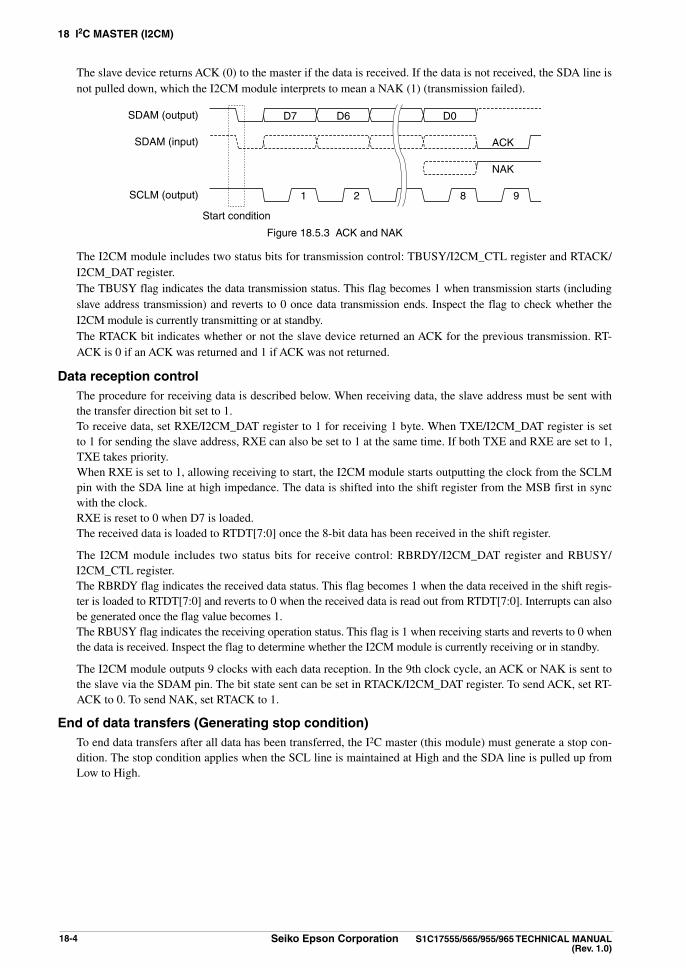
18 i2C MaSTeR (i2CM)
18-4 Seiko epson Corporation S1C17555/565/955/965 TeChniCal Manual (Rev. 1.0)
The slave device returns ACK (0) to the master if the data is received. If the data is not received, the SDA line is not pulled down, which the I2CM module interprets to mean a NAK (1) (transmission failed).
SDAM (output)
SDAM (input)
SCLM (output)
Start condition
1 2 8 9
D7 D6 D0
ACK
NAK
5.3 ACK and NAKFigure 18.
The I2CM module includes two status bits for transmission control: TBUSY/I2CM_CTL register and RTACK/I2CM_DAT register.
The TBUSY flag indicates the data transmission status. This flag becomes 1 when transmission starts (including slave address transmission) and reverts to 0 once data transmission ends. Inspect the flag to check whether the I2CM module is currently transmitting or at standby.
The RTACK bit indicates whether or not the slave device returned an ACK for the previous transmission. RT-ACK is 0 if an ACK was returned and 1 if ACK was not returned.
Data reception control The procedure for receiving data is described below. When receiving data, the slave address must be sent with
the transfer direction bit set to 1. To receive data, set RXE/I2CM_DAT register to 1 for receiving 1 byte. When TXE/I2CM_DAT register is set
to 1 for sending the slave address, RXE can also be set to 1 at the same time. If both TXE and RXE are set to 1, TXE takes priority.
When RXE is set to 1, allowing receiving to start, the I2CM module starts outputting the clock from the SCLM pin with the SDA line at high impedance. The data is shifted into the shift register from the MSB first in sync with the clock.
RXE is reset to 0 when D7 is loaded. The received data is loaded to RTDT[7:0] once the 8-bit data has been received in the shift register.
The I2CM module includes two status bits for receive control: RBRDY/I2CM_DAT register and RBUSY/ I2CM_CTL register.
The RBRDY flag indicates the received data status. This flag becomes 1 when the data received in the shift regis-ter is loaded to RTDT[7:0] and reverts to 0 when the received data is read out from RTDT[7:0]. Interrupts can also be generated once the flag value becomes 1.
The RBUSY flag indicates the receiving operation status. This flag is 1 when receiving starts and reverts to 0 when the data is received. Inspect the flag to determine whether the I2CM module is currently receiving or in standby.
The I2CM module outputs 9 clocks with each data reception. In the 9th clock cycle, an ACK or NAK is sent to the slave via the SDAM pin. The bit state sent can be set in RTACK/I2CM_DAT register. To send ACK, set RT-ACK to 0. To send NAK, set RTACK to 1.
end of data transfers (Generating stop condition) To end data transfers after all data has been transferred, the I2C master (this module) must generate a stop con-
dition. The stop condition applies when the SCL line is maintained at High and the SDA line is pulled up from Low to High.

18 i2C MaSTeR (i2CM)
S1C17555/565/955/965 TeChniCal Manual Seiko epson Corporation 18-5(Rev. 1.0)
SDAM (output)
SCLM (output)
Stop condition
5.4 Stop ConditionFigure 18.
The stop condition is generated by setting STP/I2CM_CTL register to 1. When STP is set to 1, the I2CM module pulls up the I2C bus SDA line from Low to High with the SCL line
maintained at High to generates a stop condition. The I2C bus subsequently switches to free state. Before STP can be set to 1, confirm that TBUSY or RBUSY is reset to 0 from 1 (this indicates that the I2CM
module has finished data transmit/receive operation) and then make the wait time longer than 1/4 of the I2C clock cycle set. When generating a stop condition to the slave device with a clock stretch function, STP must be set to 1 after data transfer (including ACK/NAK transfer) has finished and the time for the slave device to finish clock stretching has elapsed. STP is reset to 0 when the stop condition is generated.
Continuing data transfer (Generating Repeated start condition) To make it possible to continue with a different data transfer after data transfer completion, the I2C master (this
module) can generate a repeated start condition.
SDAM (output)
SCLM (output)
Repeated start condition
5.5 Repeated Start ConditionFigure 18.
The repeated start condition is generated by setting STRT/I2CM_CTL register to 1 when the I2C bus is busy. STRT is automatically reset to 0 once the repeated start condition is generated. Slave address transmission is
subsequently possible with the I2C bus remaining in the busy state.
Disabling data transfer After the stop condition has been generated, write 0 to I2CMEN to disable data transfers. To determine whether
the stop condition has been generated, check to see if STP is automatically cleared to 0 after it is set to 1 by polling.
When I2CMEN is set to 0 while the I2C bus is in busy status, the SCLM and SDAM output levels and transfer data at that point cannot be guaranteed.
Timing chart
PCLK
T16 Ch.2 output
SCLM
SDAM
STRT
STRT settingStart condition I2C bus busy
5.6 Start Condition GenerationFigure 18.

18 i2C MaSTeR (i2CM)
18-6 Seiko epson Corporation S1C17555/565/955/965 TeChniCal Manual (Rev. 1.0)
TXE setting Transmit data settingTransmission end
Transmission start
PCLK
T16 Ch.2 output
SCLM
SDAM
TXE
TBUSY
RTACK
RTDT[7:0]
Interrupt
D[7:0] D[7:0]
A6/D7 A5/D6 DIR/D0 ACK
ACK receiving
5.7 Slave Address Transmission/Data TransmissionFigure 18.
RXE setting ACK transmitting Receiving endReceiving start
PCLK
T16 Ch.2 output
SCLM
SDAM
RXE
RBUSY
RTACK
RTDT[7:0]
RBRDY/Interrupt
D[7:0]
D7 D6 ACKD0
5.8 Data ReceivingFigure 18.
PCLK
T16 Ch.2 output
SCLM
SDAM
STP
STP settingStop condition I2C bus free
5.9 Stop Condition GenerationFigure 18.
i2CM interrupts18.6 The I2CM module includes a function for generating the following two different types of interrupts. • Transmit buffer empty interrupt • Receive buffer full interrupt
The I2CM module outputs one interrupt signal shared by the two above interrupt causes to the interrupt controller (ITC).

18 i2C MaSTeR (i2CM)
S1C17555/565/955/965 TeChniCal Manual Seiko epson Corporation 18-7(Rev. 1.0)
Transmit buffer empty interrupt To use this interrupt, set TINTE/I2CM_ICTL register to 1. If TINTE is set to 0 (default), interrupt requests for
this cause will not be sent to the ITC. If transmit buffer empty interrupts are enabled (TINTE = 1), an interrupt request is output to the ITC as soon as
the transmit data set in RTDT[7:0]/I2CM_DAT register is transferred to the shift register. An interrupt occurs if other interrupt conditions are satisfied.
Checking whether a transmit buffer empty interrupt has occurred or not A transmit buffer empty interrupt has occurred if TXE/I2CM_DAT register is read as 0 in the procedure
shown below.(1) Set TINTE/I2CM_ICTL register to 1.(2) Write data to RTDT[7:0]/I2CM_DAT register.(3) Set TXE/I2CM_DAT register to 1. (This can be performed simultaneously with Step 2 above.)(4) An I2CM interrupt occurs.(5) Read TXE/I2CM_DAT register.
Clearing the cause of transmit buffer empty interrupt Write data to RTDT[7:0]/I2CM_DAT register.
notes: • Data will not be sent if TXE/I2CM_DAT register is set to 0.
• If RTDT[7:0] contains data received from the I2C bus, it will be overwritten.
Receive buffer full interrupt To use this interrupt, set RINTE/I2CM_ICTL register to 1. If RINTE is set to 0 (default), interrupt requests for
this cause will not be sent to the ITC. If receive buffer full interrupts are enabled (RINTE = 1), an interrupt request is output to the ITC as soon as the
data received in the shift register is loaded to RTDT[7:0]. An interrupt occurs if other interrupt conditions are met.
Checking whether a receive buffer full interrupt has occurred or not A receive buffer full interrupt has occurred if RBRDY/I2CM_DAT register is read as 1 in the procedure
shown below.(1) Set RINTE/I2CM_ICTL register to 1.(2) An I2CM interrupt occurs.(3) Read RBRDY/I2CM_DAT register.
Clearing the cause of receive buffer full interrupt Read data from RTDT[7:0]/I2CM_DAT register.
For more information on interrupt processing, see the “Interrupt Controller (ITC)” chapter.
Control Register Details18.7
7.1 List of I2CM RegistersTable 18.
address Register name Function0x4340 I2CM_EN I2C Master Enable Register Enables the I2C master module.0x4342 I2CM_CTL I2C Master Control Register Controls the I2C master operation and indicates transfer status.0x4344 I2CM_DAT I2C Master Data Register Transmit/receive data
0x4346 I2CM_ICTL I2C Master Interrupt Control Register Controls the I2C master interrupt.
The I2CM module registers are described in detail below.
note: When data is written to the registers, the “Reserved” bits must always be written as 0 and not 1.

18 i2C MaSTeR (i2CM)
18-8 Seiko epson Corporation S1C17555/565/955/965 TeChniCal Manual (Rev. 1.0)
i2C Master enable Register (i2CM_en)Register name address Bit name Function Setting init. R/W Remarks
i2C Master en-able Register(i2CM_en)
0x4340(16 bits)
D15–1 – reserved – – – 0 when being read.
D0 i2CMen I2C master enable 1 Enable 0 Disable 0 R/W
D[15:1] Reserved
D0 i2CMen: i2C Master enable Bit Enables or disables I2CM module operation. 1 (R/W): Enabled 0 (R/W): Disabled (default) Setting I2CMEN to 1 starts the I2CM module operation, enabling data transfer. Setting I2CMEN to 0
stops the I2CM module operation.
i2C Master Control Register (i2CM_CTl)Register name address Bit name Function Setting init. R/W Remarks
i2C Master Con-trol Register(i2CM_CTl)
0x4342(16 bits)
D15–10 – reserved – – – 0 when being read.D9 RBuSY Receive busy flag 1 Busy 0 Idle 0 RD8 TBuSY Transmit busy flag 1 Busy 0 Idle 0 R
D7–5 – reserved – – – 0 when being read.D4 nSeRM Noise remove on/off 1 On 0 Off 0 R/W
D3–2 – reserved – – – 0 when being read.D1 STP Stop control 1 Stop 0 Ignored 0 R/WD0 STRT Start control 1 Start 0 Ignored 0 R/W
D[15:10] Reserved
D9 RBuSY: Receive Busy Flag Bit Indicates the I2CM receiving status. 1 (R): Operating 0 (R): Standby (default)
RBUSY is set to 1 when the I2CM starts data receiving and is maintained at 1 while receiving is under-way. It is cleared to 0 once reception is completed.
D8 TBuSY: Transmit Busy Flag Bit Indicates the I2CM transmission status. 1 (R): Operating 0 (R): Standby (default)
TBUSY is set to 1 when the I2CM starts data transmission and is maintained at 1 while transmission is underway. It is cleared to 0 once transmission is completed.
D[7:5] Reserved
D4 nSeRM: noise Remove On/Off Bit Turns the noise filter function on or off. 1 (R/W): On 0 (R/W): Off (default)
The I2CM module includes a function for filtering noise from the SDAM and SCLM pin input signals. This function is enabled by setting NSERM to 1. Note that using this function requires setting the I2CM clock (T16 Ch.2 output clock) frequency to 1/6 or less of PCLK.
D[3:2] Reserved
D1 STP: Stop Control Bit Generates the stop condition. 1 (R/W): Stop condition generated 0 (R/W): Ineffective (default)

18 i2C MaSTeR (i2CM)
S1C17555/565/955/965 TeChniCal Manual Seiko epson Corporation 18-9(Rev. 1.0)
By setting STP to 1, the I2CM module generates the stop condition by pulling up the I2C bus SDA line from Low to High with the SCL line maintaining at High. The I2C bus subsequently becomes free. Note that the stop condition will be generated only if STP is 1 and TXE/I2CM_DAT register, RXE/I2CM_DAT register, and STRT are set to 0 when data transfer is completed (including ACK transfer). STP is automatically reset to 0 if the stop condition is generated.
D0 STRT: Start Control Bit Generates the start condition. 1 (R/W): Start condition generated 0 (R/W): Ineffective (default)
By setting STRT to 1, the I2CM module generates the start condition by pulling down the I2C bus SDA line to Low with SCL line maintaining at High.
The repeated start condition can be generated by setting STRT to 1 when the I2C bus is busy. STRT is automatically reset to 0 once the start condition or repeated start condition is generated. The
I2C bus subsequently becomes busy.
i2C Master Data Register (i2CM_DaT)Register name address Bit name Function Setting init. R/W Remarks
i2C Master Data Register(i2CM_DaT)
0x4344(16 bits)
D15–12 – reserved – – – 0 when being read.D11 RBRDY Receive buffer ready flag 1 Ready 0 Empty 0 RD10 RXe Receive execution 1 Receive 0 Ignored 0 R/WD9 TXe Transmit execution 1 Transmit 0 Ignored 0 R/WD8 RTaCK Receive/transmit ACK 1 Error 0 ACK 0 R/W
D7–0 RTDT[7:0] Receive/transmit dataRTDT7 = MSBRTDT0 = LSB
0x0 to 0xff 0x0 R/W
D[15:12] Reserved
D11 RBRDY: Receive Buffer Ready Flag Bit Indicates the receive buffer status. 1 (R): Receive data exists 0 (R): No receive data (default)
The RBRDY flag becomes 1 when the data received in the shift register is loaded to RTDT[7:0] and reverts to 0 when the receive data is read out from RTDT[7:0]. Interrupts can also be generated once the flag value becomes 1.
D10 RXe: Receive execution Bit Receives 1 byte of data. 1 (R/W): Data reception start 0 (R/W): Ineffective (default) Setting RXE to 1 and TXE to 0 starts receiving for 1 byte of data. RXE can be set to 1 for subsequent re-
ception, even if the slave address is being sent or data is being received. RXE is reset to 0 as soon as D7 is loaded to the shift register.
D9 TXe: Transmit execution Bit Transmits 1 byte of data. 1 (R/W): Data transmission start 0 (R/W): Ineffective (default)
Transmission is started by setting the transmit data to RTDT[7:0] and writing 1 to TXE. TXE can be set to 1 for subsequent transmission, even if the slave address or data is being sent. TXE is reset to 0 as soon as the data set in RTDT[7:0] is transferred to the shift register.

18 i2C MaSTeR (i2CM)
18-10 Seiko epson Corporation S1C17555/565/955/965 TeChniCal Manual (Rev. 1.0)
D8 RTaCK: Receive/Transmit aCK Bit
When transmitting data Indicates the response bit status. 1 (R/W): Error (NAK) 0 (R/W): ACK (default)
RTACK becomes 0 when ACK is returned from the slave after 1 byte of data is sent, indicating that the slave has received the data correctly. If RTACK is 1, the slave device is not operating or the data was not received correctly.
When receiving data Sets the response bit sent to the slave. 1 (R/W): Error (NAK) 0 (R/W): ACK (default)
To return an ACK after data has been received, RTACK should be set to 0 before the I2CM module sends the response bit. To return a NAK, set RTACK to 1.
D[7:0] RTDT[7:0]: Receive/Transmit Data Bits
When transmitting data Sets the transmit data. (Default: 0x0) Data transmission is started by setting TXE to 1. If a slave address or data is currently being transmit-
ted, transmission begins once the previous transmission is completed. Serial converted data is output from the SDAM pin with MSB leading and bits set to 0 as Low level. A cause of transmit buffer empty interrupt is generated as soon as the data written to this register is transferred to the shift register, after which the subsequent transmission data can be written.
When receiving data The received data can be read out. (Default: 0x0) Data reception is started by setting RXE to 1. If a slave address is currently being transmitted or data
is currently being received, the new reception starts once the previous data has been transferred. The RBRDY flag is set and a cause of receive buffer full interrupt generated as soon as reception is com-pleted and the shift register data is transferred to this register. Data can then be read until the subsequent data has been received. If the subsequent data is received before this register is read out, the contents are overwritten by the most recent received data. Serial data input from the SDAM pin with MSB lead-ing is converted to parallel, with the High level bit set to 1 and the Low level bit set to 0, then loaded to this register.
i2C Master interrupt Control Register (i2CM_iCTl)Register name address Bit name Function Setting init. R/W Remarks
i2C Master interrupt Control Register(i2CM_iCTl)
0x4346(16 bits)
D15–2 – reserved – – – 0 when being read.D1 RinTe Receive interrupt enable 1 Enable 0 Disable 0 R/WD0 TinTe Transmit interrupt enable 1 Enable 0 Disable 0 R/W
D[15:2] Reserved
D1 RinTe: Receive interrupt enable Bit Enables or disables I2CM receive buffer full interrupts. 1 (R/W): Enabled 0 (R/W): Disabled (default)
Setting RINTE to 1 enables the output of I2CM interrupt requests to the ITC due to a receive data buf-fer full. These interrupt requests are generated when the data received in the shift register is transferred to RTDT[7:0]/I2CM_DAT register (when reception is completed).
I2CM interrupts are not generated by receive data buffer full if RINTE is set to 0.

18 i2C MaSTeR (i2CM)
S1C17555/565/955/965 TeChniCal Manual Seiko epson Corporation 18-11(Rev. 1.0)
D0 TinTe: Transmit interrupt enable Bit Enables or disables I2CM transmit buffer empty interrupts. 1 (R/W): Enabled 0 (R/W): Disabled (default)
Setting TINTE to 1 enables the output of I2CM interrupt requests to the ITC due to a transmit buffer empty. These interrupt requests are generated when the data written to RTDT[7:0] is transferred to the shift register.
I2CM interrupts are not generated by transmit buffer empty if TINTE is set to 0.
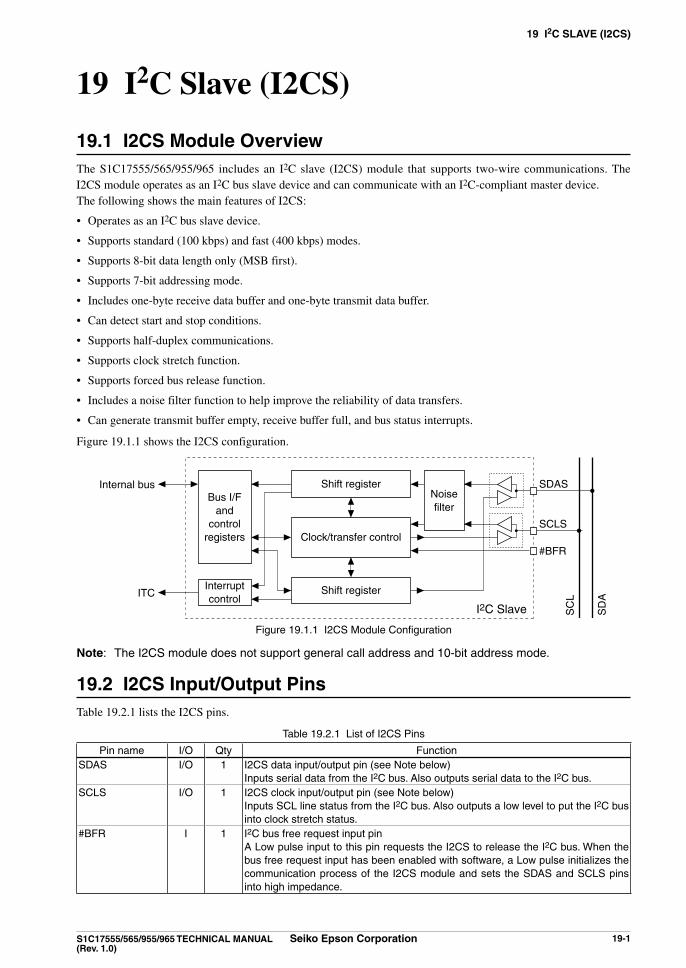
19 i2C SlaVe (i2CS)
S1C17555/565/955/965 TeChniCal Manual Seiko epson Corporation 19-1(Rev. 1.0)
I19 2C Slave (I2CS)
i2CS Module Overview19.1 The S1C17555/565/955/965 includes an I2C slave (I2CS) module that supports two-wire communications. The I2CS module operates as an I2C bus slave device and can communicate with an I2C-compliant master device. The following shows the main features of I2CS:
• Operates as an I2C bus slave device.
• Supports standard (100 kbps) and fast (400 kbps) modes.
• Supports 8-bit data length only (MSB first).
• Supports 7-bit addressing mode.
• Includes one-byte receive data buffer and one-byte transmit data buffer.
• Can detect start and stop conditions.
• Supports half-duplex communications.
• Supports clock stretch function.
• Supports forced bus release function.
• Includes a noise filter function to help improve the reliability of data transfers.
• Can generate transmit buffer empty, receive buffer full, and bus status interrupts.
Figure 19.1.1 shows the I2CS configuration.
SCLS
#BFR
Shift register SDAS
SD
A
SC
L
Internal bus
ITC
I2C Slave
Bus I/Fand
controlregisters
Shift register
Clock/transfer control
Noisefilter
Interruptcontrol
1.1 I2CS Module ConfigurationFigure 19.
note: The I2CS module does not support general call address and 10-bit address mode.
i2CS input/Output Pins19.2 Table 19.2.1 lists the I2CS pins.
2.1 List of I2CS PinsTable 19.
Pin name I/O Qty FunctionSDAS I/O 1 I2CS data input/output pin (see Note below)
Inputs serial data from the I2C bus. Also outputs serial data to the I2C bus. SCLS I/O 1 I2CS clock input/output pin (see Note below)
Inputs SCL line status from the I2C bus. Also outputs a low level to put the I2C bus into clock stretch status.
#BFR I 1 I2C bus free request input pinA Low pulse input to this pin requests the I2CS to release the I2C bus. When the bus free request input has been enabled with software, a Low pulse initializes the communication process of the I2CS module and sets the SDAS and SCLS pins into high impedance.

19 i2C SlaVe (i2CS)
19-2 Seiko epson Corporation S1C17555/565/955/965 TeChniCal Manual (Rev. 1.0)
The I2CS input/output pins (SDAS, SCLS, #BFR) are shared with I/O ports and are initially set as general purpose I/O port pins. The pin functions must be switched using the port function select bits to use the general purpose I/O port pins as I2CS input/output pins. For detailed information on pin function switching, see the “I/O Ports (P)” chap-ter.
note: The pins go to high impedance status when the port function is switched. The SCLS and SDAS pins do not output a high level, so these lines should be pulled up to HVDD
with an external pull-up resistor. Be sure to avoid pulling these pins up to a voltage that exceeds the HVDD level.
I2C master
I2CS I2C slave
SCLSSDAS
HVDD
2.1 IFigure 19. 2C Connection Example
Operation Clock19.3 The I2CS module operates with the clock output from the external I2C master device by inputting it from the SCLS pin. The I2CS module also uses the peripheral module clock (PCLK) for its operations. The PCLK frequency must be set eight-times or higher than the SCLS input clock frequency during data transfer. In standby status, use of the asynchronous address detection function allows the application to lower the PCLK clock frequency to reduce cur-rent consumption. For more information, see “Asynchronous address detection function” in Section 19.4.3.
initializing i2CS19.4
Reset19.4.1
The I2CS module must be reset to initialize the communication process and to set the I2C bus into free status (high impedance). The following shows two methods for resetting the module:
(1) Software reset The I2CS module can be reset using SOFTRESET/I2CS_CTL register. To reset the I2CS module, write 1 to SOFTRESET to place the I2CS module into reset status, then write 0 to
SOFTRESET to release it from reset status. It is not necessary to insert a waiting time between writing 1 and 0. The I2CS module initializes the I2C communication process and put the SDAS and SCLS pins into high-im-
pedance to be ready to detect a start condition. Furthermore, the I2CS control bits except for SOFTRESET are initialized. Perform the software reset in the initial setting process before staring communication.
(2) Bus free request with an input from the #BFR pin The I2CS module can accept bus free requests via the #BFR pin. The bus free request support is disabled by
default. To enable this function, set BFREQ_EN/I2CS_CTL register to 1. When this function is enabled, a low pulse (One peripheral module clock (PCLK) cycles or more pulse width is
required. Two PCLK clock cycles or more pulse width is recommended.) input to the #BFR pin sets BFREQ/I2CS_STAT register to 1. This initializes the I2C communication process and puts the SDAS and SCLS pins into high-impedance. The control registers will not be initialized as distinct from the software reset described above.
note: When BFREQ is set to 1 (an interrupt can be used for checking this status), perform a software reset and set the registers again.

19 i2C SlaVe (i2CS)
S1C17555/565/955/965 TeChniCal Manual Seiko epson Corporation 19-3(Rev. 1.0)
Setting Slave address19.4.2
I2C devices have a unique slave address to identify each device.The I2CS module supports 7-bit address (does not support 10-bit address), and the address of this module must be set to SADRS[6:0]/I2CS_SADRS register.
Optional Functions19.4.3
The I2CS module has a clock stretch, asynchronous address detection, and noise filter optional functions selectable in the application program.
Clock stretch function After data and ACK are transmitted or received, the slave device may issue a wait request to the master device
until it is ready to transmit/receive by pulling the I2C bus SCL line down to low. The I2CS module supports this clock stretch function.
The master device enters a standby state until the wait request is canceled (the SCL line goes high). The clock stretch function in this module is disabled by default. When using the clock stretch function, set CLKSTR_EN/I2CS_CTL register to 1 before starting data communication. Note that the data setup time (after the SDAS pin outputs the MSB of SDATA[7:0]/I2CS_TRNS register until I2CS turns the SCLS pin pull-down resistor off) while the I2CS module is operating with the clock stretch function enabled varies depending on the I2CS mod-ule operating clock (PCLK) frequency.
asynchronous address detection function The I2CS module operation clock (PCLK) frequency must be set eight-times or higher than the transfer rate
during data transfer. However, the PCLK frequency can be lowered to reduce current consumption if no other processing is required during standby for data transfer. The asynchronous address detection function is provided to detect the I2C slave address sent from the master in this status.
The asynchronous address detection function in this module is disabled by default. When using the asynchro-nous address detection function, set ASDET_EN/I2CS_CTL register to 1.
If the slave address sent from the master has matched with one that has been set in this I2CS module when the asynchronous address detection function has been enabled, the I2CS module generates a bus status interrupt and returns NAK to the I2C master to request for resending the slave address.
Set the PCLK frequency to eight-times or higher than the transfer rate and reset ASDET_EN to 0 in the inter-rupt handler routine. Data transfer will be able to resume normally after the master retries transmission. After the master generates a stop condition to put the I2C bus into free status, the asynchronous address detection function can be enabled again to lower the operating speed.
notes: • When the asynchronous address detection function is enabled, the I2C bus signals are input without passing through the noise filter. Therefore, the slave address may not be detected in a high-noise environment.
• When the asynchronous address detection function is enabled, data transfer cannot be per-formed even if the PCLK frequency is eight-times or higher than the transfer rate. Be sure to disable the asynchronous address detection function during normal operation.
noise filter The I2CS module includes a function to remove noise from the SDAS and SCLS input signals. This function is
enabled by setting NF_EN/I2CS_CTL register to 1.
Data Transfer Control19.5 Make the following settings before starting data transfers. (1) Initialize the I2CS module. See Section 19.4.(2) Set the interrupt conditions to use I2CS interrupt. See Section 19.6.
note: Make sure that the I2CS module is disabled (I2CSEN/I2CS_CTL register = 0) before setting the conditions above.

19 i2C SlaVe (i2CS)
19-4 Seiko epson Corporation S1C17555/565/955/965 TeChniCal Manual (Rev. 1.0)
enabling data transfers First, set I2CSEN/I2CS_CTL register to 1 to enable I2CS operation. This makes the I2CS in ready-to-transmit/
receive status in which a start condition can be detected.
note: Do not set the I2CSEN bit to 0 while the I2CS module is transmitting/receiving data.
Starting data transfer To start data transmission/reception, set COM_MODE/I2CS_CTL register to 1 to enable data communications. When the slave address for this module that has been sent from the master is received after a start condition is
detected, the I2CS module returns an ACK (SDAS = low) and starts operating for data reception or data trans-mission according to the transfer direction bit that has been received with the slave address.
When COM_MODE is 0 (default), the I2CS module does not send back a response if the master has sent the slave address of this module (it is regarded as that the I2CS module has returned a NAK to the master).
SDAS (input)
SDAS (output)
SCLS (input)
Start condition
1 2 3 4 5 6 7 8 9
ACK
NAK
7-bit slave address
Transfer direction0: master → slave (data reception)1: slave → master (data transmission)
A6 A5D7 D6
A4D5
A3D4
A2D3
A1D2
A0D1
R/WD0
5.1 Receiving Slave Address and Data Direction BitFigure 19.
When a start condition is detected, BUSY/I2CS_ASTAT register is set to 1 to indicate that the I2C bus is put into busy status. When the slave address of this module is received, SELECTED/I2CS_ASTAT register is set to 1 to indicate that this module has been selected as the I2C slave device. BUSY is maintained at 1 until a stop condition is detected. SELECTED is maintained at 1 until a stop condition or repeated start condition is de-tected.
The value of the transfer direction bit is set to R/W/I2CS_ASTAT register, so use R/W to select the transmit- or receive-handling.
If the slave address of this module is detected when the asynchronous address detection function has been en-abled, ASDET/I2CS_STAT register is set to 1. The I2CS module generates a bus status interrupt and returns NAK to the I2C master to request for resending the slave address. Set the PCLK frequency to eight-times or higher than the transfer rate and disable the asynchronous address detection function in the interrupt handler routine. Data transfer will be able to resume normally after the master retries transmission. ASDET can be cleared by writing 1.
Data transmission The following describes a data transmission procedure. The I2CS module starts data transmission process when both SELECTED and R/W are set to 1. It sets TXEMP/
I2CS_ASTAT register to 1 to issue a request to the application program to write transmit data. Write transmit data to SDATA[7:0]/I2CS_TRNS register.
When setting the first transmit data after this module has been selected as the slave device, follow the precau-tions described below.
When the clock stretch function is disabled (default) Transmit data must be written to SDATA[7:0] within 1 cycle of the I2C clock (SCLS input clock) after TX-
EMP has been set to 1. This time is not enough for data preparation, so write transmit data before TXEMP has been set to 1. If the previous transmit data is still stored in SDATA[7:0], it is overwritten with the new data to be transferred. Therefore, the clear operation (see below) using TBUF_CLR is unnecessary.

19 i2C SlaVe (i2CS)
S1C17555/565/955/965 TeChniCal Manual Seiko epson Corporation 19-5(Rev. 1.0)
When the asynchronous address detection function is used, the data written before ASDET_EN is reset to 0 becomes invalid. Therefore, transmission data must be written after TXEMP has been set to 1.
When the clock stretch function is enabled The master device is placed into wait status by the clock stretch function, so transmit data can be written
after TXEMP is set. However, if the previous transmit data is still stored in SDATA[7:0], it will be sent im-mediately after TXEMP has been set. In order to avoid this problem, clear the I2CS_TRNS register using TBUF_CLR/I2CS_CTL register before this module is selected as the slave device. The I2CS_TRNS regis-ter is cleared by writing 1 to TBUF_CLR then writing 0 to it.
It is not necessary to clear the I2CS_TRNS register if the first transmit data is written before TXEMP has been set.
When the asynchronous address detection function is used, the data written before ASDET_EN is reset to 0 becomes invalid. Therefore, transmission data must be written after TXEMP has been set to 1.
For writing transmit data other than the first time, use an interrupt that can be generated when TXEMP is set to 1. TXEMP is also set to 1 when the transmit data written to SDATA[7:0] is loaded to the sift register during transmission. TXEMP is cleared by writing transmit data to SDATA[7:0].
When the clock stretch function is disabled (default) When the clock stretch function has been disabled, data must be written to the I2CS_TRNS register within
7 cycles of the I2C clock (SCLS input clock) from TXEMP being set to 1. If data has not been written in this period, the current register value (previous transmit data) will be sent.
In this case, TXUDF/I2CS_STAT register is set to 1 to indicate that invalid data has been sent. An interrupt can be generated when TXUDF is set to 1, so an error handling should be performed in the interrupt han-dler routine. TXUDF is cleared by writing 1.
When the clock stretch function is enabled When the clock stretch function has been enabled, the I2CS module pulls down the SCLS pin to low to
generate a clock stretch (wait) status until transmit data is written to the I2CS_TRNS register.
Transmit data bits are output from the SDAS pin in sync with the SCLS input clock sent from the master. The MSB is output first. After the eight bits has been output, the master sends back an ACK or NAK in the ninth clock cycle.
SDAS (output)
SDAS (input)
SCLS (input) 1 2 8 9
D7 D6 D0
ACK
NAK
5.2 ACK and NAKFigure 19.
The ACK bit indicates that the master could receive data. It is also a transmit request bit, therefore, the next transmit data must be written in advance. Receiving an ACK generates a clock stretch status when the clock stretch function has been enabled, so data can be written after an ACK is received.
A NAK will be returned from the master if the master could not receive data or when the master terminates data reception. In this case a clock stretch status is not generated even if the clock stretch function has been enabled.
Read DA_NAK/I2CS_STAT register to check if an ACK is returned or if a NAK is returned. DA_NAK is set to 0 when an ACK is returned or set to 1 when a NAK is returned. An interrupt can be generated when DA_NAK is set to 1, so an error or termination handling can be performed in the interrupt handler routine. DA_NAK is cleared by writing 1.
The SDA line status during data transmission is input in the module and is compare with the output data. The comparison results are set to DMS/I2CS_STAT register. DMS is set to 0 when data is output correctly. If the SDA line status is different from the output data, DMS is set to 1. This may be caused by a low pull-up resistor value or another device that is controlling the SDA line. An interrupt can be generated when DMS is set to 1, so an error handling can be performed in the interrupt handler routine. DMS is cleared by writing 1.

19 i2C SlaVe (i2CS)
19-6 Seiko epson Corporation S1C17555/565/955/965 TeChniCal Manual (Rev. 1.0)
note: If the I2CS module has sent back a NAK as the response to the address sent by the master when the conditions shown below are all met, the master must wait for 33 µs or more before it can send another slave address (except when the master sends the I2CS slave address again).1. The transfer rate is set to 320 kbps or higher.2. The asynchronous address detection function is enabled.3. The I2CS module is placed into transfer standby state and OSC1 is used as the operating
clock (PCLK).
Data reception The following describes a data receive procedure. The I2CS module starts data receiving process when SELECTED is set to 1 and R/W is set to 0. The received
data bits are input from the SDAS pin in sync with the SCLS input clock sent from the master. When the eight-bit data (MSB first) is received in the shift register, the received data is loaded to RDATA[7:0]/I2CS_RECV register.
When the received data is loaded to RDATA[7:0], RXRDY/I2CS_ASTAT register is set to 1 to issue a request to the application program to read RDATA[7:0]. An interrupt can be generated when RXRDY is set to 1, so the received data should be read in the interrupt handler routine. RXRDY is cleared by reading the received data.
When the clock stretch function is disabled (default) When the clock stretch function has been disabled, data must be read from the I2CS_RECV register within
7 cycles of the I2C clock (SCLS input clock) from RXRDY being set to 1.
When the clock stretch function is enabled When the clock stretch function has been enabled, the I2CS module pulls down the SCLS pin to low to
generate a clock stretch (wait) status until the received data is read from the I2CS_RECV register.
If the next data has been received without reading the received data, RDATA[7:0] will be overwritten. In this case, RXOVF/I2CS_STAT register is set to 1 to indicate that the received data has been overwritten. An inter-rupt can be generated when RXOVF is set to 1, so an error handling should be performed in the interrupt han-dler routine. RXOVF is cleared by writing 1.
To return naK during data reception During data reception (master transmission), the I2CS module sends back an ACK (SDAS = low) every time an
8-bit data has been received (by default setting). The response code can be changed to NAK (SDAS = Hi-Z) by setting NAK_ANS/I2CS_CTL register. An ACK will be sent when NAK_ANS is 0 or a NAK will be sent when NAK_ANS is set to 1.
NAK_ANS should be set within 7 cycles of the I2C clock (SCLS input clock) after RXRDY has been set to 1 by receiving data just prior to one required for returning NAK.
SCLS (input)
SDAS (input)
SDAS (output)
RXRDY
NAK_ANS
NAK_ANS setting periodReceive interrupt
6 7 8 9 1
D0D2 D1 D7 D6 D5 D4 D3 D2 D0D1
ACK NAK
2 3 4 5 6 7 8 9
5.3 NAK_ANS Setting and NAK Response TimingFigure 19.
end of data transfer (detecting stop condition) Data transfers will be terminated when the master generates a stop condition. The stop condition is a state in
which the SDA line is pulled up from Low to High with the SCL line maintained at High.

19 i2C SlaVe (i2CS)
S1C17555/565/955/965 TeChniCal Manual Seiko epson Corporation 19-7(Rev. 1.0)
SDAS (input)
SCLS (input)
Stop condition
5.4 Stop ConditionFigure 19.
If a stop condition is detected while the I2CS module is selected as the slave device (SELECTED = 1), the I2CS module sets DA_STOP/I2CS_STAT register to 1. At the same time, it sets the SDAS and SCLS pins into high-impedance and initializes the I2C communication process to enter standby state that is ready to detect the next start condition. Also SELECTED and BUSY are reset to 0.
An interrupt can be generated when DA_STOP is set to 1, so a communication terminating process should be performed in the interrupt handler routine. DA_STOP is cleared by writing 1.
Disabling data transfer After data transfer has finished, write 0 to the COM_MODE/I2CS_CTL register to disable data transfer. Always make sure that BUSY and SELECTED are 0 before disabling data transfer. To deactivate the I2CS module, set I2CSEN/I2CS_CTL register to 0.
Timing charts
PCLK
SCLS (input)
SCLS (output)
SDAS (input)
SDAS (output)
R/W
BUSY
SELECTED
TXEMP
TXUDF
DA_NAK
DA_STOP
Transmit data shift register
SDATA[7:0]
Interrupt
A6
H/L
valid
D[7:0]
A5 A4 A3 A2 A1 A0
D7 D6 ACK
Start conditionSlave address reception Data transmissionClock stretch
Transmit interrupt Transmit interrupt
Transmit data is set.
shift
R/W = 1
PCLK x 6
5.5 I2CS Timing Chart 1 (start condition → data transmission)Figure 19.
D5 D4 D3 D2 D1 D0D0' D6D7D0'
valid shift shift shift shift shift shift shiftshift
ACK
PCLK
SCLS (input)
SCLS (output)
SDAS (input)
SDAS (output)
R/W
BUSY
SELECTED
TXEMP
TXUDF
DA_NAK
DA_STOP
Transmit data shift register
SDATA[7:0]
Interrupt
Data transmissionData transmission Clock stretch
Bus status interruptTransmit data is set.
PCLK x 6
NAK
D[7:0]
Transmit interrupt
Stop condition
5.6 I2CS Timing Chart 2 (data transmission → stop condition)Figure 19.

19 i2C SlaVe (i2CS)
19-8 Seiko epson Corporation S1C17555/565/955/965 TeChniCal Manual (Rev. 1.0)
sift shift shift shift shift shift shift shift
D7
PCLK
SCLS (input)
SCLS (output)
SDAS (input)
SDAS (output)
R/W
BUSY
SELECTED
RXRDY
RXOVF
DA_STOP
Receive data sift register
RDATA[7:0]
Interrupt
A6 A5 A4 A3 A2 A1 A0 D6 D5R/W = 0
ACK
Slave address reception Data reception
shiftshift
Start condition
5.7 I2CS Timing Chart 3 (start condition → data reception)Figure 19.
D[7:0]' D[7:0]
D5 D4 D3 D2 D1 D0D7 D6D0'
shift shift shift shift shift shift shiftshift
ACK
PCLK
SCLS (input)
SCLS (output)
SDAS (input)
SDAS (output)
R/W
BUSY
SELECTED
RXRDY
RXOVF
DA_STOP
Receive data sift register
RDATA[7:0]
Interrupt
Data receptionData reception Clock stretch
NAK
Receive interrupt Receive interrupt
Bus status interruptReceive data is read.
Stop condition
5.8 I2CS Timing Chart 4 (data reception → stop condition)Figure 19.
i2CS interrupts19.6 The I2CS module includes a function for generating the following three different types of interrupts. • Transmit interrupt • Receive interrupt • Bus status interrupt
The I2CS module outputs one interrupt signal shared by the three above interrupt causes to the interrupt controller (ITC).
Transmit interrupt When the transmit data written to SDATA[7:0]/I2CS_TRNS register is sent to the shift register, TXEMP/I2CS_
ASTAT register is set to 1 and an interrupt signal is output to the ITC. An interrupt occurs if other interrupt con-ditions are satisfied. This interrupt can be used to write the next transmit data to SDATA[7:0].
Set TXEMP_IEN/I2CS_ICTL register to 1 when using this interrupt. If TXEMP_IEN is set to 0 (default), inter-rupt requests by this cause will not be sent to the ITC.
Receive interrupt When the received data is loaded to RDATA[7:0]/I2CS_RECV register, RXRDY/I2CS_ASTAT register is set to
1 and an interrupt signal is output to the ITC. An interrupt occurs if other interrupt conditions are satisfied. This interrupt can be used to read the received data from RDATA[7:0].
Set RXRDY_IEN/I2CS_ICTL register to 1 when using this interrupt. If RXRDY_IEN is set to 0 (default), in-terrupt requests by this cause will not be sent to the ITC.

19 i2C SlaVe (i2CS)
S1C17555/565/955/965 TeChniCal Manual Seiko epson Corporation 19-9(Rev. 1.0)
Bus status interrupt The I2CS module provides the status bits listed below to represent the transmit/receive and I2C bus statuses (see
Section 19.5 for details of each function).
1. ASDET/I2CS_STAT register: This bit is set to 1 when the slave address is detected by the asynchronous ad-dress detection function.
2. TXUDF/I2CS_STAT register: This bit is set to 1 when a transmit operation has started before transmit data is written. (When the clock stretch function is disabled)
3. DA_NAK/I2CS_STAT register: This bit is set to 1 when a NAK is returned from the master during trans-mission.
4. DMS/I2CS_STAT register: This bit is set to 1 when the SDA line status is different from transfer data. DMS will also be set to 1 when another slave device issues ACK to this I2C slave address (when ASDET_
EN/I2CS_CTL register = 0).
Note: When the master device of the I2C bus, which has multiple slave devices connected includ-ing this IC, starts communication with another slave device, the I2CS module issues NAK in response to the sent slave address. On the other hand, the selected slave device issues ACK. Therefore, DMS may be set due to a difference between the output value of this IC and the SDA line status. When SELECTED/I2CS_ASTAT register is set to 0, you can ig-nore DMS without a problem even if it is set to 1 as there is a difference in the response code (ACK/NAK) from the selected slave device.
When the I2CS module is placed into asynchronous address detection mode (ASDET_EN = 1), a DMS does not occur as in the condition above.
5. RXOVF/I2CS_STAT register: This bit is set to 1 when the next data has been received before the received data is read (the received data is overwritten). (When the clock stretch function is disabled)
6. BFREQ/I2CS_STAT register: This bit is set to 1 when a bus free request is accepted.
7. DA_STOP/I2CS_STAT register: This bit is set to 1 if a stop condition or a repeated start condition is de-tected while this module is selected as the slave device.
When one of the bits listed above is set to 1, BSTAT/I2CS_STAT register is set to 1 and an interrupt signal is output to the ITC. An interrupt occurs if other interrupt conditions are satisfied. This interrupt can be used to perform an error or terminate handling.
Set BSTAT_IEN/I2CS_ICTL register to 1 when using this interrupt. If BSTAT_IEN is set to 0 (default), inter-rupt requests by this cause will not be sent to the ITC.
For more information on interrupt processing, see the “Interrupt Controller (ITC)” chapter.
Control Register Details19.7
7.1 List of I2CS RegistersTable 19.
address Register name Function0x4360 I2CS_TRNS I2C Slave Transmit Data Register I2C slave transmit data0x4362 I2CS_RECV I2C Slave Receive Data Register I2C slave receive data0x4364 I2CS_SADRS I2C Slave Address Setup Register Sets the I2C slave address.
0x4366 I2CS_CTL I2C Slave Control Register Controls the I2C slave module.0x4368 I2CS_STAT I2C Slave Status Register Indicates the I2C bus status.0x436a I2CS_ASTAT I2C Slave Access Status Register Indicates the I2C slave access status.0x436c I2CS_ICTL I2C Slave Interrupt Control Register Controls the I2C slave interrupt.
The I2CS module registers are described in detail below.
note: When data is written to the registers, the “Reserved” bits must always be written as 0 and not 1.

19 i2C SlaVe (i2CS)
19-10 Seiko epson Corporation S1C17555/565/955/965 TeChniCal Manual (Rev. 1.0)
i2C Slave Transmit Data Register (i2CS_TRnS)Register name address Bit name Function Setting init. R/W Remarks
i2C Slave Transmit Data Register(i2CS_TRnS)
0x4360(16 bits)
D15–8 – reserved – – – 0 when being read.D7–0 SDaTa[7:0] I2C slave transmit data 0–0xff 0x0 R/W
D[15:8] Reserved
D[7:0] SDaTa[7:0]: i2C Slave Transmit Data Bits Sets a transmit data in this register. (Default: 0x0) The serial-converted data is output from the SDAS pin beginning with the MSB, in which the bits set to
0 are output as Low-level signals. When the data set in this register is sent to the shift register, a trans-mit interrupt occurs. The next transmit data can be written to the register after that.
If the clock stretch function has been disabled, data must be written to this register within 7 cycles of the I2C clock (SCLS input clock) after a transmit interrupt has been occurred.
However, when setting the first transmit data after this module has been selected as the slave device, follow the precautions described below.
When the clock stretch function is disabled (default) Transmit data must be written to SDATA[7:0] within 1 cycle of the I2C clock (SCL1 input clock)
after TXEMP has been set to 1. This time is not enough for data preparation, so write transmit data before TXEMP has been set to 1. If the previous transmit data is still stored in SDATA[7:0], it is overwritten with the new data to be transferred. Therefore, the clear operation (see below) using TBUF_CLR is unnecessary.
When the asynchronous address detection function is used, the data written before ASDET_EN is re-set to 0 becomes invalid. Therefore, transmission data must be written after TXEMP has been set to 1.
When the clock stretch function is enabled The master device is placed into wait status by the clock stretch function, so transmit data can be
written after TXEMP is set. However, if the previous transmit data is still stored in SDATA[7:0], it will be sent immediately after TXEMP has been set. In order to avoid this problem, clear the I2CS_TRNS register using TBUF_CLR/I2CS_CTL register before this module is selected as the slave device. The I2CS_TRNS register is cleared by writing 1 to TBUF_CLR then writing 0 to it.
It is not necessary to clear the I2CS_TRNS register if the first transmit data is written before TX-EMP has been set.
When the asynchronous address detection function is used, the data written before ASDET_EN is re-set to 0 becomes invalid. Therefore, transmission data must be written after TXEMP has been set to 1.
i2C Slave Receive Data Register (i2CS_ReCV)Register name address Bit name Function Setting init. R/W Remarks
i2C Slave Receive Data Register(i2CS_ReCV)
0x4362(16 bits)
D15–8 – reserved – – – 0 when being read.D7–0 RDaTa[7:0] I2C slave receive data 0–0xff 0x0 R
D[15:8] Reserved
D[7:0] RDaTa[7:0]: i2C Slave Receive Data Bits The received data can be read from this register. (Default: 0x0) The serial data input from the SDA1 pin beginning with the MSB is converted into parallel data, with
the high-level signals changed to 1 and the low-level signals changed to 0. The resulting data is stored in this register.
When a receive operation is completed and the data received in the shift register is loaded to this register, RXRDY/I2CS_ASTAT register is set and a receive interrupt occurs. Thereafter, the data can be read out.
When the clock stretch function has been disabled, data must be read from this register within 7 cycles of the I2C clock (SCL1 input clock) after RXRDY is set to 1. If the next data has been received without reading the received data, this register will be overwritten with the newly received data.

19 i2C SlaVe (i2CS)
S1C17555/565/955/965 TeChniCal Manual Seiko epson Corporation 19-11(Rev. 1.0)
i2C Slave address Setup Register (i2CS_SaDRS)Register name address Bit name Function Setting init. R/W Remarks
i2C Slave address Setup Register(i2CS_SaDRS)
0x4364(16 bits)
D15–7 – reserved – – – 0 when being read.D6–0 SaDRS[6:0] I2C slave address 0–0x7f 0x0 R/W
D[15:7] Reserved
D[6:0] SaDRS[6:0]: i2CS address Bits Sets the slave address of the I2CS module to this register. (Default: 0x0)
i2C Slave Control Register (i2CS_CTl)Register name address Bit name Function Setting init. R/W Remarks
i2C SlaveControl Register(i2CS_CTl)
0x4366(16 bits)
D15–9 – reserved – – – 0 when being read.D8 TBuF_ClR I2CS_TRNS register clear 1 Clear state 0 Normal 0 R/WD7 i2CSen I2C slave enable 1 Enable 0 Disable 0 R/WD6 SOFTReSeT Software reset 1 Reset 0 Cancel 0 R/WD5 naK_anS NAK answer 1 NAK 0 ACK 0 R/WD4 BFReQ_en Bus free request enable 1 Enable 0 Disable 0 R/WD3 ClKSTR_en Clock stretch On/Off 1 On 0 Off 0 R/WD2 nF_en Noise filter On/Off 1 On 0 Off 0 R/WD1 aSDeT_en Async.address detection On/Off 1 On 0 Off 0 R/WD0 COM_MODe I2C slave communication mode 1 Active 0 Standby 0 R/W
D[15:9] Reserved
D8 TBuF_ClR: i2CS_TRnS Register Clear Bit Clears the I2CS_TRNS register. 1 (R/W): Clear state 0 (R/W): Normal state (clear state cancellation) (default)
When TBUF_CLR is set to 1, the I2CS_TRNS register enters clear state. After that writing 0 to TBUF_CLR returns the I2CS_TRNS register to normal state. It is not necessary to insert a waiting time be-tween writing 1 and 0.
If a new transmission is started when the I2CS_TRNS register still stores data for the previous trans-mission that has already finished, the data will be sent when TXEMP/I2CS_ASTAT register is set. In order to avoid this problem, clear the I2CS_TRNS register using TBUF_CLR before starting transmis-sion (before slave selection). The clear operation is not required if transmit data is written to the I2CS_TRNS register before TXEMP is set to 1.
Data can be written to the I2CS_TRNS register even if it is placed into clear state (TBUF_CLR = 1). However, this writing does not reset TXEMP to 0. Note that TXEMP is not reset to 0 when TBUF_CLR is set back to 0. Therefore, data must be written to the I2CS_TRNS register when TBUF_CLR = 0.
D7 i2CSen: i2C Slave enable Bit Enables or disables operations of the I2CS module. 1 (R/W): Enabled 0 (R/W): Disabled (default)
When I2CSEN is set to 1, the I2CS module is activated and data transfer is enabled. When I2CSEN is set to 0, the I2CS module goes off.
D6 SOFTReSeT: Software Reset Bit Resets the I2CS module. 1 (R/W): Reset 0 (R/W): Cancel reset state (default)
To reset the I2CS module, write 1 to SOFTRESET to place the I2CS module into reset status, then write 0 to SOFTRESET to release it from reset status. It is not necessary to insert a waiting time be-tween writing 1 and 0. The I2CS module initializes the I2C communication process and put the SDAS and SCLS pins into high-impedance to be ready to detect a start condition. Furthermore, the I2CS con-trol bits except for SOFTRESET are initialized. Perform the software reset in the initial setting process before staring communication.
19 i2C SlaVe (i2CS)
19-12 Seiko epson Corporation S1C17555/565/955/965 TeChniCal Manual (Rev. 1.0)
D5 naK_anS: naK answer Bit Specifies the acknowledge bit to be sent after data reception. 1 (R/W): NAK 0 (R/W): ACK (default)
When an eight-bit data is received, the I2CS module sends back an ACK (SDAS = low) or a NAK (SDAS = Hi-Z). Either ACK or NAK should be specified using NAK_ANS within 7 cycles of the I2C clock (SCLS input clock) after RXRDY has been set to 1 by receiving the previous data.
D4 BFReQ_en: Bus Free Request enable Bit Enables or disables I2C bus free requests by inputting a low pulse to the #BFR pin. 1 (R/W): Enabled 0 (R/W): Disabled (default)
To accept I2C bus free requests, set BFREQ_EN to 1. When a bus free request is accepted, BFREQ/I2CS_STAT register is set to 1. This initializes the I2C communication process and puts the SDAS and SCLS pins into high-impedance. The control registers will not be initialized in this process.
When BFREQ_EN is set to 0, low pulse inputs to the #BFR pin are ignored and BFREQ is not set to 1.
D3 ClKSTR_en: Clock Stretch On/Off Bit Turns the clock stretch function on or off. 1 (R/W): On 0 (R/W): Off (default)
After data and ACK are transmitted or received, the slave device may issue a wait request to the master device until it is ready to transmit/receive by pulling the I2C bus SCL line down to Low. The I2CS mod-ule supports this clock stretch function. The master device enters a standby state until the wait request is canceled (the SCL line goes high). When using the clock stretch function, set CLKSTR_EN to 1 before starting data communication.
D2 nF_en: noise Filter On/Off Bit Turns the noise filter on or off. 1 (R/W): On 0 (R/W): Off (default)
The I2CS module contains a function to remove noise from the SDAS and SCLS input signals. This function is enabled by setting NF_EN to 1.
D1 aSDeT_en: async. address Detection On/Off Bit Turns the asynchronous address detection function on or off. 1 (R/W): On 0 (R/W): Off (default)
The I2CS module operation clock (PCLK) frequency must be set eight-times or higher than the transfer rate during data transfer. However, the PCLK frequency can be lowered to reduce current consumption if no other processing is required during standby for data transfer.
The asynchronous address detection function is provided to detect the I2C slave address sent from the master in this status. This function is enabled by setting ASDET_EN to 1. If the slave address sent from the master has matched with one that has been set in this I2CS module when the asynchronous address detection function has been enabled, the I2CS module generates a bus status interrupt and returns NAK to the I2C master to request for resending the slave address. Set the PCLK frequency to eight-times or higher than the transfer rate and reset ASDET_EN to 0 in the interrupt handler routine. Data transfer will be able to resume normally after the master retries transmission. After the master generates a stop condition to put the I2C bus into free status, the asynchronous address detection function can be enabled again to lower the operating speed.
notes: • When the asynchronous address detection function is enabled, the I2C bus signals are input without passing through the noise filter. Therefore, the slave address may not be detected in a high-noise environment.
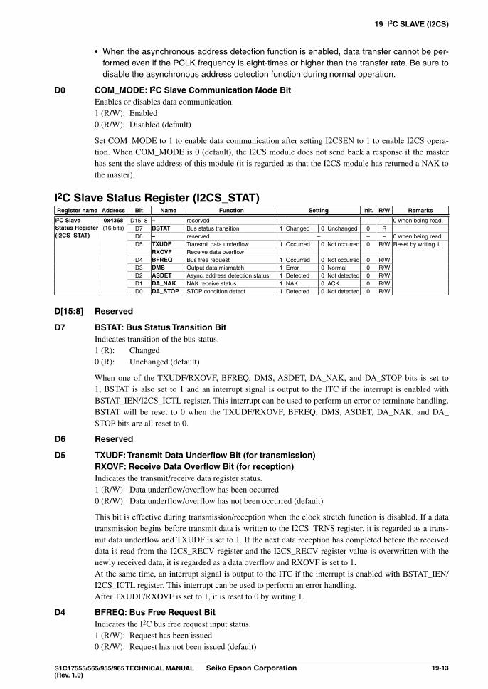
19 i2C SlaVe (i2CS)
S1C17555/565/955/965 TeChniCal Manual Seiko epson Corporation 19-13(Rev. 1.0)
• When the asynchronous address detection function is enabled, data transfer cannot be per-formed even if the PCLK frequency is eight-times or higher than the transfer rate. Be sure to disable the asynchronous address detection function during normal operation.
D0 COM_MODe: i2C Slave Communication Mode Bit Enables or disables data communication. 1 (R/W): Enabled 0 (R/W): Disabled (default)
Set COM_MODE to 1 to enable data communication after setting I2CSEN to 1 to enable I2CS opera-tion. When COM_MODE is 0 (default), the I2CS module does not send back a response if the master has sent the slave address of this module (it is regarded as that the I2CS module has returned a NAK to the master).
i2C Slave Status Register (i2CS_STaT)Register name address Bit name Function Setting init. R/W Remarks
i2C SlaveStatus Register(i2CS_STaT)
0x4368(16 bits)
D15–8 – reserved – – – 0 when being read.D7 BSTaT Bus status transition 1 Changed 0 Unchanged 0 RD6 – reserved – – – 0 when being read.D5 TXuDF Transmit data underflow 1 Occurred 0 Not occurred 0 R/W Reset by writing 1.
RXOVF Receive data overflowD4 BFReQ Bus free request 1 Occurred 0 Not occurred 0 R/WD3 DMS Output data mismatch 1 Error 0 Normal 0 R/WD2 aSDeT Async. address detection status 1 Detected 0 Not detected 0 R/WD1 Da_naK NAK receive status 1 NAK 0 ACK 0 R/WD0 Da_STOP STOP condition detect 1 Detected 0 Not detected 0 R/W
D[15:8] Reserved
D7 BSTaT: Bus Status Transition Bit Indicates transition of the bus status. 1 (R): Changed 0 (R): Unchanged (default)
When one of the TXUDF/RXOVF, BFREQ, DMS, ASDET, DA_NAK, and DA_STOP bits is set to 1, BSTAT is also set to 1 and an interrupt signal is output to the ITC if the interrupt is enabled with BSTAT_IEN/I2CS_ICTL register. This interrupt can be used to perform an error or terminate handling. BSTAT will be reset to 0 when the TXUDF/RXOVF, BFREQ, DMS, ASDET, DA_NAK, and DA_STOP bits are all reset to 0.
D6 Reserved
D5 TXuDF: Transmit Data underflow Bit (for transmission) RXOVF: Receive Data Overflow Bit (for reception) Indicates the transmit/receive data register status. 1 (R/W): Data underflow/overflow has been occurred 0 (R/W): Data underflow/overflow has not been occurred (default)
This bit is effective during transmission/reception when the clock stretch function is disabled. If a data transmission begins before transmit data is written to the I2CS_TRNS register, it is regarded as a trans-mit data underflow and TXUDF is set to 1. If the next data reception has completed before the received data is read from the I2CS_RECV register and the I2CS_RECV register value is overwritten with the newly received data, it is regarded as a data overflow and RXOVF is set to 1.
At the same time, an interrupt signal is output to the ITC if the interrupt is enabled with BSTAT_IEN/I2CS_ICTL register. This interrupt can be used to perform an error handling.
After TXUDF/RXOVF is set to 1, it is reset to 0 by writing 1.
D4 BFReQ: Bus Free Request Bit Indicates the I2C bus free request input status. 1 (R/W): Request has been issued 0 (R/W): Request has not been issued (default)

19 i2C SlaVe (i2CS)
19-14 Seiko epson Corporation S1C17555/565/955/965 TeChniCal Manual (Rev. 1.0)
If BFREQ_EN/I2CS_CTL register has been set to 1 (bus free request enabled), a low pulse longer than five peripheral module clock (PCLK) cycles input to the #BFR pin sets BFREQ to 1 and the bus free request is accepted. When a bus free request is accepted, the I2CS module initializes the I2C commu-nication process and puts the SDAS and SCLS pins into high-impedance. The control registers will not be initialized in this process. At the same time, an interrupt signal is output to the ITC if the interrupt is enabled with BSTAT_IEN/I2CS_ICTL register. This interrupt can be used to perform an error handling.
After BFREQ is set to 1, it is reset to 0 by writing 1. If BFREQ_EN is set to 0, low pulse inputs to the #BFR pin are ignored and BFREQ is not set to 1.
D3 DMS: Output Data Mismatch Bit Represents the results of comparison between output data and SDA line status. 1 (R/W): Error has been occurred 0 (R/W): Error has not been occurred (default)
The I2C bus SDA line status during data transmission is input in the module and is compared with the output data. The comparison results are set to DMS. DMS is set to 0 when data is output correctly. If the SDA line status is different from the output data, DMS is set to 1. This may be caused by a low pull-up resistor value or another device that is controlling the SDA line. At the same time, an interrupt signal is output to the ITC if the interrupt is enabled with BSTAT_IEN/I2CS_ICTL register. This interrupt can be used to perform an error handling. After DMS is set to 1, it is reset to 0 by writing 1.
note: When the master device of the I2C bus, which has multiple slave devices connected includ-ing this IC, starts communication with another slave device, the I2CS module of this IC issues NAK in response to the sent slave address. On the other hand, the selected slave device is-sues ACK. Therefore, DMS may be set due to a difference between the output value of this IC and the SDA line status. When SELECTED/I2CS_ASTAT register is set to 0, you can ignore DMS without a problem even if it is set to 1 as there is a difference in the response code (ACK/NAK) from the selected slave device.
When the I2CS module is placed into asynchronous address detection mode (ASDET_EN = 1), a DMS does not occur as in the condition above.
D2 aSDeT: async. address Detection Status Bit Indicates the asynchronous address detection status. 1 (R/W): Detected 0 (R/W): Not detected (default)
The I2CS module operation clock (PCLK) frequency must be set eight-times or higher than the transfer rate during data transfer. However, the PCLK frequency can be lowered to reduce current consumption if no other processing is required during standby for data transfer. The asynchronous address detection function is provided to detect the I2C slave address sent from the master in this status. ASDET is set to 1 if the slave address of the I2CS module is detected when the asynchronous address detection function has been enabled by setting ASDET_EN/I2CS_CTL register.
The I2CS module returns a NAK to the I2C master to request for resending the slave address. At the same time, an interrupt signal is output to the ITC if the interrupt is enabled with BSTAT_IEN/I2CS_ICTL register. Set the PCLK frequency to eight-times or higher than the transfer rate and reset ASDET_EN to 0 in the interrupt handler routine. Data transfer will be able to resume normally after the master retries transmission. After ASDET is set to 1, it is reset to 0 by writing 1.
D1 Da_naK: naK Receive Status Bit Indicates the acknowledge bit returned from the master. 1 (R/W): NAK 0 (R/W): ACK (default)
DA_NAK is set to 0 when an ACK is returned from the master after an eight-bit data has been sent. This indicates that the master could receive data. If DA_NAK is 1, it indicates that the master could not receive data or the master terminates data reception. At the same time DA_NAK is set to 1, an interrupt signal is output to the ITC if the interrupt is enabled with BSTAT_IEN/I2CS_ICTL register. This inter-rupt can be used to perform an error handling. After DA_NAK is set to 1, it is reset to 0 by writing 1.

19 i2C SlaVe (i2CS)
S1C17555/565/955/965 TeChniCal Manual Seiko epson Corporation 19-15(Rev. 1.0)
D0 Da_STOP: Stop Condition Detect Bit Indicates that a stop condition or a repeated start condition is detected. 1 (R/W): Detected 0 (R/W): Not detected (default)
If a stop condition or a repeated start condition is detected while the I2CS module is selected as the slave device (SELECTED/I2CS_ASTAT register = 1), the I2CS module sets DA_STOP to 1. At the same time, it initializes the I2C communication process.
When DA_STOP is set to 1, an interrupt signal is output to the ITC if the interrupt is enabled with BSTAT_IEN/I2CS_ICTL register. This interrupt can be used to perform a terminate handling. After DA_STOP is set to 1, it is reset to 0 by writing 1.
i2C Slave access Status Register (i2CS_aSTaT)Register name address Bit name Function Setting init. R/W Remarks
i2C Slave access Status Register(i2CS_aSTaT)
0x436a(16 bits)
D15–5 – reserved – – – 0 when being read.D4 RXRDY Receive data ready 1 Ready 0 Not ready 0 RD3 TXeMP Transmit data empty 1 Empty 0 Not empty 0 RD2 BuSY I2C bus status 1 Busy 0 Free 0 RD1 SeleCTeD I2C slave select status 1 Selected 0 Not selected 0 RD0 R/W Read/write direction 1 Output 0 Input 0 R
D[15:5] Reserved
D4 RXRDY: Receive Data Ready Bit Indicates that the received data is ready to read. 1 (R): Received data ready 0 (R): No received data (default)
When the received data is loaded to the I2CS_RECV register, RXRDY is set to 1. At the same time, an interrupt signal is output to the ITC if the interrupt is enabled with RXRDY_IEN/I2CS_ICTL register. This interrupt can be used to read the received data from the I2CS_RECV register.
After RXRDY is set to 1, it is reset to 0 when the I2CS_RECV register is read.
D3 TXeMP: Transmit Data empty Bit Indicates that transmit data can be written. 1 (R): Transmit data empty (data can be written) 0 (R): Transmit data still stored (data cannot be written) (default)
When the transmit data written to the I2CS_TRNS register is sent, TXEMP is set to 1. At the same time, an interrupt signal is output to the ITC if the interrupt is enabled with TXEMP_IEN/I2CS_ICTL register. This interrupt can be used to write the next transmit data to the I2CS_TRNS register.
After TXEMP is set to 1, it is reset to 0 when data is written to the I2CS_TRNS register.
D2 BuSY: i2C Bus Status Bit Indicates the I2C bus status. 1 (R): Bus busy status 0 (R): Bus free status (default)
When the I2CS module detects a start condition or detects that the SCLS or SDAS signal goes low, BUSY is set to 1 to indicate that the I2C bus enters busy status. The slave select status whether this module is selected as the slave device or not does not affect the BUSY status. After BUSY is set to 1, it is reset to 0 when a STOP condition is detected.
D1 SeleCTeD: i2C Slave Select Status Bit Indicates that this module is selected as the I2C slave device. 1 (R): Selected 0 (R): Not selected (default)
When the slave address that is set in this module is received, SELECTED is set to 1 to indicate that this module is selected as the I2C slave device. After SELECTED is set to 1, it is reset to 0 when a stop con-dition or a repeated start condition is detected.

19 i2C SlaVe (i2CS)
19-16 Seiko epson Corporation S1C17555/565/955/965 TeChniCal Manual (Rev. 1.0)
D0 R/W: Read/Write Direction Bit Represents the transfer direction bit value. 1 (R): Output (master read operation) 0 (R): Input (master write operation) (default)
The transfer direction bit value that has been received with the slave address is set to R/W. Use R/W to select the transmit- or receive-handling.
i2C Slave interrupt Control Register (i2CS_iCTl)Register name address Bit name Function Setting init. R/W Remarks
i2C Slave interrupt Control Register(i2CS_iCTl)
0x436c(16 bits)
D15–3 – reserved – – – 0 when being read.D2 BSTaT_ien Bus status interrupt enable 1 Enable 0 Disable 0 R/WD1 RXRDY_ien Receive interrupt enable 1 Enable 0 Disable 0 R/WD0 TXeMP_ien Transmit interrupt enable 1 Enable 0 Disable 0 R/W
D[15:3] Reserved
D2 BSTaT_ien: Bus Status interrupt enable Bit Enables or disables the bus status interrupt. 1 (R/W): Enabled 0 (R/W): Disabled (default)
When BSTAT_IEN is set to 1, I2C bus status interrupt requests to the ITC are enabled. A bus status in-terrupt request occurs when BSTAT/I2CS_STAT register is set to 1. (See description of BSTAT.)
When BSTAT_IEN is set to 0, a bus status interrupt will not be generated.
D1 RXRDY_ien: Receive interrupt enable Bit Enables or disables the I2CS receive interrupt. 1 (R/W): Enabled 0 (R/W): Disabled (default)
When RXRDY_IEN is set to 1, I2CS receive interrupt requests to the ITC are enabled. A receive inter-rupt request occurs when the data received in the shift register is loaded to the I2CS_RECV register (receive operation completed). When RXRDY_IEN is set to 0, a receive interrupt will not be generated.
D0 TXeMP_ien: Transmit interrupt enable Bit Enables or disables the I2CS transmit interrupt. 1 (R/W): Enabled 0 (R/W): Disabled (default)
When TXEMP_IEN is set to 1, I2CS transmit interrupt requests to the ITC are enabled. A transmit in-terrupt request occurs when the data written to the I2CS_TRNS register is transferred to the shift regis-ter. When TXEMP_IEN is set to 0, a transmit interrupt will not be generated.

20 iR ReMOTe COnTROlleR (ReMC) [S1C17565/965]
S1C17555/565/955/965 TeChniCal Manual Seiko epson Corporation 20-1(Rev. 1.0)
IR Remote Controller (REMC) 20 [S1C17565/965]
note: The IR remote controller (REMC) is unavailable in the S1C17555/955.
ReMC Module Overview20.1 The S1C17565/965 includes an IR remote controller (REMC) module for transmitting/receiving infrared remote control communication signals. The following shows the features of the REMC module:
• Supports input and output infrared remote control communication signals.
• Includes a carrier generator for generating a carrier signal.
• Includes an 8-bit down-counter for counting the transfer data length.
• Includes a modulator for generating transmission data of the specified carrier length.
• Includes an edge detector for detecting input signal rising and falling edges.
• Can generate counter underflow interrupts indicating that the specified data length has been sent and input rising/falling edge detection interrupts for data receive processing.
Figure 20.1.1 shows the configuration of the REMC module.
Carrier generator
Internal bus
IR remote controller
Bus I/Fand
controlregisters Data length counter
REMO
REMIEdge detector
Modulator
Interruptcontrol
PCLKCLG
Divider(1/1–1/16K)
ITC
1.1 REMC Module ConfigurationFigure 20.
ReMC input/Output Pins20.2 Table 20.2.1 lists the REMC input/output pins.
2.1 List of REMC PinsTable 20.
Pin name i/O Qty Function
REMI I 1 Remote control receive data input pinInputs receive data.
REMO O 1 Remote control transmit data output pinOutputs modulated remote control transmit data.
The REMC input/output pins (REMI, REMO) are shared with I/O ports and are initially set as general purpose I/O port pins. The pin functions must be switched using the port function select bits to use the general purpose I/O port pins as REMC input/output pins.For detailed information on pin function switching, see the “I/O Ports (P)” chapter.

20 iR ReMOTe COnTROlleR (ReMC) [S1C17565/965]
20-2 Seiko epson Corporation S1C17555/565/955/965 TeChniCal Manual (Rev. 1.0)
Carrier Generation20.3 The REMC module includes a carrier generator that generates a carrier signal for transmission in accordance with the clock set by software and carrier H and L section lengths.
The carrier generation clock is generated by dividing PCLK into 1/1 to 1/16K. The division ratio can be selected from the 15 types shown below using CGCLK[3:0]/REMC_CFG register.
3.1 Carrier Generation Clock (PCLK Division Ratio) SelectionTable 20.
CGClK[3:0] Division ratio CGClK[3:0] Division ratio
0xf Reserved 0x7 1/1280xe 1/16384 0x6 1/640xd 1/8192 0x5 1/320xc 1/4096 0x4 1/160xb 1/2048 0x3 1/80xa 1/1024 0x2 1/40x9 1/512 0x1 1/20x8 1/256 0x0 1/1
(Default: 0x0)
notes: • The clock generator (CLG) must be configured to supply PCLK to the peripheral modules be-fore running the REMC.
• Make sure the REMC is halted before setting the clock.
For detailed information on the CLG control, see the “Clock Generator (CLG)” chapter.
The carrier H and L section lengths are set by REMCH[5:0]/REMC_CAR register and REMCL[5:0]/REMC_CAR register, respectively. Set a value corresponding to the number of clock (selected as above) cycles + 1 to these regis-ters. The carrier H and L section lengths can be calculated as follows:
REMCH + 1Carrier H section length = —————— [s] cg_clk
REMCL + 1Carrier L section length = —————— [s] cg_clk
REMCH: Carrier H section length data valueREMCL: Carrier L section length data valuecg_clk: Carrier generation clock frequency
The carrier signal is generated from these settings as shown in Figure 20.3.1.
Example: CGCLK[3:0] = 0x2 (PCLK/4), REMCH[5:0] = 2, REMCL[5:0] = 1
PCLK
Carrier generation clock
Count
Carrier
0 1 2 0 1 0
Carrier H section length Carrier L section length
3.1 Carrier Signal GenerationFigure 20.
Data length Counter Clock Settings20.4 The data length counter is an 8-bit counter for setting data lengths when transmitting data. When a value corresponding to the data pulse width is written during data transmission, the data length counter begins counting down from that value and stops after generating an underflow interrupt cause when the counter reaches 0. The subsequent transmit data is set using this interrupt.

20 iR ReMOTe COnTROlleR (ReMC) [S1C17565/965]
S1C17555/565/955/965 TeChniCal Manual Seiko epson Corporation 20-3(Rev. 1.0)
This counter is also used for data receiving, enabling measurement of the received data length. Interrupts can be generated at the input signal rising or falling edges when receiving data. The data pulse length can be obtained from the difference between data pulse edges by setting the data length counter to 0xff using the interrupt when the input changes and by reading out the count value when a subsequent interrupt occurs due to input changes. This data length counter clock also uses a divided PCLK clock and can select one of 15 different types. The divi-sion ratio to generate the data length counter clock is selected by LCCLK[3:0]/REMC_CFG register provided sepa-rately to the carrier generation clock select bits.
4.1 Data Length Counter Clock (PCLK Division Ratio) SelectionTable 20.
lCClK[3:0] Division ratio lCClK[3:0] Division ratio
0xf Reserved 0x7 1/1280xe 1/16384 0x6 1/640xd 1/8192 0x5 1/320xc 1/4096 0x4 1/160xb 1/2048 0x3 1/80xa 1/1024 0x2 1/40x9 1/512 0x1 1/20x8 1/256 0x0 1/1
(Default: 0x0)
The data length counter can count up to 256. The count clock should be selected to ensure that the data length fits within this range.
Data Transfer Control20.5 Make the following settings before starting data transfers.(1) Configure the carrier signal. (See Section 20.3.)(2) Select the data length counter clock. (See Section 20.4.)(3) Set the interrupt conditions. (See Section 20.6.)
note: Make sure the REMC module is halted (REMEN/REMC_CFG register = 0) before changing the above settings.
Data transmission control
REMDT
REMO pin output
Carrier
REMDT
REMO pin output
5.1 Data TransmissionFigure 20.
PCLK
Data length counter clock
REMLEN[7:0]
Interrupt signal
4 3 2 1 0
5.2 Underflow Interrupt Generation TimingFigure 20.
(1) Data transmit mode setting Set REMC to transmit mode by writing 0 to REMMD/REMC_CFG register.

20 iR ReMOTe COnTROlleR (ReMC) [S1C17565/965]
20-4 Seiko epson Corporation S1C17555/565/955/965 TeChniCal Manual (Rev. 1.0)
(2) Enabling data transmission Enable REMC operation by setting REMEN/REMC_CFG register to 1. This initiates REMC transmission.
Set REMDT/REMC_LCNT register to 0 and REMLEN[7:0]/REMC_LCNT register to 0x0 before setting REMEN to 1 to prevent unnecessary data transmission.
(3) Transmission data setting Set the data to be transmitted (High or Low) to REMDT/REMC_LCNT register. Setting REMDT to 1 outputs High; setting it to 0 outputs Low from the REMO pin after being modulated by
the carrier signal.
(4) Data pulse length setting Set the value corresponding to the data pulse length (High or Low section) to REMLEN[7:0]/REMC_LCNT
register to set to the data length counter. Given below is the value to which the data length counter is set:
Setting value = Data pulse length (seconds) × Data length counter clock frequency (Hz)
The data length counter starts counting down from the value written using the data length counter clock selected. A cause of underflow interrupt occurs when the data length counter value reaches 0. If the interrupt is enabled,
an REMC interrupt request is output to the interrupt controller (ITC). The data length counter stops counting at the same time with the counter value 0 maintained.
(5) Interrupt handling To transmit the subsequent data, set the subsequent data (Step 3) and set the data pulse length (Step 4) in the
interrupt handler routine executed by the data length counter underflow.
(6) Terminating data transmission To terminate data transmission, set REMEN to 0 after the final data transmission has completed (after an under-
flow interrupt has occurred).
Data reception control
PCLK
Data length counter clock
REMI input
REMDT(Sampled waveform)
REMRIF
REMFIF
Interrupt signal
REMLEN[7:0]Write 0xff
x+2 x+1 x 0xff 0xfe 0xfd 0xffWrite 0xff
Write 1
Write 1
5.3 Data ReceptionFigure 20.
(1) Data receive mode setting Set REMC to receive mode by writing 1 to REMMD/REMC_CFG register.
(2) Enabling data reception Enable REMC operation by setting REMEN/REMC_CFG register to 1. This initiates REMC reception (input
edge detection). REMC detects an input transition (signal rising or falling edges) by sampling the input signal from the REMI
pin using the carrier generation clock. If a signal edge is detected, a cause of rising or falling edge interrupt is generated. An REMC interrupt request is output to the ITC if the interrupt is enabled. Rising edge and falling edge interrupts can be individually enabled or disabled.

20 iR ReMOTe COnTROlleR (ReMC) [S1C17565/965]
S1C17555/565/955/965 TeChniCal Manual Seiko epson Corporation 20-5(Rev. 1.0)
Note that if the signal level after the input has changed is not detected for at least two continuous sampling clock cycles, the input signal transition is interpreted as noise, and no rising or falling edge interrupt is gener-ated.
(3) Interrupt handling When a rising edge or falling edge interrupt occurs, write 0xff to REMLEN[7:0]/REMC_LCNT register in the
interrupt handler routine to set the value to the data length counter.
The data length counter starts counting down using the selected data length counter clock from the value writ-ten.
The data received can be read out from REMDT/REMC_LCNT register.
The subsequent falling or rising edge interrupt is generated at the termination of the data pulse. Read the data length counter at that point. The data length can be calculated from the difference between 0xff and the value read. To receive the subsequent data, set the data length counter to 0xff once again, then wait for the subsequent interrupt.
If the data length counter becomes 0 after being set to 0xff without the occurrence of an edge interrupt, either no more data is left or a receive error has occurred. Data length counter underflow interrupts are generated even when receiving data and should be used for terminate/error handling.
(4) Terminating data reception To terminate data reception, write 0 to REMEN after the final data has been received.
ReMC interrupts20.6 The REMC module includes a function for generating the following three different types of interrupts.• Underflow interrupt• Rising edge interrupt• Falling edge interrupt
The REMC module outputs one interrupt signal shared by the three interrupt causes above to the interrupt controller (ITC). To identify the cause of interrupt occurred, check the interrupt flag status in the REMC module.
underflow interrupt Generated when the data length counter has counted down to 0, this interrupt cause sets the interrupt flag RE-
MUIF/REMC_INT register inside the REMC to 1. When data is being transmitted, the underflow interrupt indicates that the specified data length has been trans-
mitted. When receiving data, the underflow interrupt indicates that data has been received or a receive error has occurred.
To use this interrupt, set REMUIE/REMC_INT register to 1. If REMUIE is set to 0 (default), the interrupt re-quest attributable to this cause will not be sent to the ITC.
When REMUIF is set to 1, REMC outputs an interrupt request to the ITC. An interrupt will be generated if the ITC and S1C17 Core interrupt conditions are met.
REMUIF should be inspected in the REMC interrupt handler routine to determine whether the REMC interrupt is attributable to data length counter underflow.
The interrupt cause should be cleared in the interrupt handler routine by resetting (writing 1 to) REMUIF.
Rising edge interrupt Generated when the REMI pin input signal changes from Low to High, this interrupt cause sets the interrupt
flag REMRIF/REMC_INT register to 1 within the REMC. By running the data length counter between this interrupt and a falling edge interrupt when data is being re-
ceived, the received data pulse width can be calculated from that count value. To use this interrupt, set REMRIE/REMC_INT register to 1. If REMRIE is set to 0 (default), the interrupt re-
quest attributable to this cause will not be sent to the ITC. When REMRIF is set to 1, REMC outputs an interrupt request to the ITC. An interrupt will be generated if the
ITC and S1C17 Core interrupt conditions are met.

20 iR ReMOTe COnTROlleR (ReMC) [S1C17565/965]
20-6 Seiko epson Corporation S1C17555/565/955/965 TeChniCal Manual (Rev. 1.0)
REMRIF should be inspected in the REMC interrupt handler routine to determine whether the REMC interrupt is attributable to input signal rising edge.
The interrupt cause should be cleared in the interrupt handler routine by resetting (writing 1 to) REMRIF.
Falling edge interrupt Generated when the REMI pin input signal changes from High to Low, this interrupt cause sets the interrupt
flag REMFIF/REMC_INT register to 1 within the REMC. By running the data length counter between this interrupt and a rising edge interrupt when data is being re-
ceived, the received data pulse width can be calculated from that count value. To use this interrupt, set REMFIE/REMC_INT register to 1. If REMFIE is set to 0 (default), the interrupt re-
quest attributable to this cause will not be sent to the ITC. When REMFIF is set to 1, REMC outputs an interrupt request to the ITC. An interrupt will be generated if the
ITC and S1C17 Core interrupt conditions are met. REMFIF should be inspected in the REMC interrupt handler routine to determine whether the REMC interrupt
is attributable to input signal falling edge. The interrupt cause should be cleared in the interrupt handler routine by resetting (writing 1 to) REMFIF.
For more information on interrupt processing, see the “Interrupt Controller (ITC)” chapter.
Control Register Details20.7
7.1 List of REMC RegistersTable 20.
address Register name Function0x5340 REMC_CFG REMC Configuration Register Controls the clock and data transfer.0x5342 REMC_CAR REMC Carrier Length Setup Register Sets the carrier H/L section lengths.
0x5344 REMC_LCNT REMC Length Counter Register Sets the transmit/receive data length.0x5346 REMC_INT REMC Interrupt Control Register Controls interrupts.
The REMC registers are described in detail below.
note: When data is written to the registers, the “Reserved” bits must always be written as 0 and not 1.
ReMC Configuration Register (ReMC_CFG)Register name address Bit name Function Setting init. R/W Remarks
ReMC Configuration Register(ReMC_CFG)S1C17565/965
0x5340(16 bits)
D15–12 CGClK[3:0] Carrier generator clock division ratio select
CGCLK[3:0]LCCLK[3:0]
Division ratio0x0 R/W Source clock = PCLK
0xf0xe0xd0xc0xb0xa0x90x80x70x60x50x40x30x20x10x0
reserved1/163841/81921/40961/20481/10241/5121/2561/1281/641/321/161/81/41/21/1
D11–8 lCClK[3:0] Length counter clock division ratio select
0x0 R/W
D7–2 – reserved – – – 0 when being read.D1 ReMMD REMC mode select 1 Receive 0 Transmit 0 R/WD0 ReMen REMC enable 1 Enable 0 Disable 0 R/W
D[15:12] CGClK[3:0]: Carrier Generator Clock Division Ratio Select Bits Selects a carrier generation clock (PCLK division ratio).

20 iR ReMOTe COnTROlleR (ReMC) [S1C17565/965]
S1C17555/565/955/965 TeChniCal Manual Seiko epson Corporation 20-7(Rev. 1.0)
7.2 Carrier Generation Clock (PCLK Division Ratio) SelectionTable 20.CGClK[3:0] Division ratio CGClK[3:0] Division ratio
0xf Reserved 0x7 1/1280xe 1/16384 0x6 1/640xd 1/8192 0x5 1/320xc 1/4096 0x4 1/160xb 1/2048 0x3 1/80xa 1/1024 0x2 1/40x9 1/512 0x1 1/20x8 1/256 0x0 1/1
(Default: 0x0)
D[11:8] lCClK[3:0]: length Counter Clock Division Ratio Select Bits Selects a data length counter clock (PCLK division ratio).
7.3 Data Length Counter Clock (PCLK Division Ratio) SelectionTable 20.
lCClK[3:0] Division ratio lCClK[3:0] Division ratio
0xf Reserved 0x7 1/1280xe 1/16384 0x6 1/640xd 1/8192 0x5 1/320xc 1/4096 0x4 1/160xb 1/2048 0x3 1/80xa 1/1024 0x2 1/40x9 1/512 0x1 1/20x8 1/256 0x0 1/1
(Default: 0x0)
note: The clock should be set only while the REMC module is stopped (REMEN = 0).
D[7:2] Reserved
D1 ReMMD: ReMC Mode Select Bit Selects the transfer direction. 1 (R/W): Reception 0 (R/W): Transmission (default)
D0 ReMen: ReMC enable Bit Enables or disables data transfer by the REMC module. 1 (R/W): Enabled 0 (R/W): Disabled (default)
Setting REMEN to 1 starts transmission or receiving in accordance with REMMD settings. Setting REMEN to 0 disables REMC module operations.
ReMC Carrier length Setup Register (ReMC_CaR)Register name address Bit name Function Setting init. R/W Remarks
ReMC Carrier length Setup Register(ReMC_CaR)S1C17565/965
0x5342(16 bits)
D15–14 – reserved – – – 0 when being read.D13–8 ReMCl[5:0] Carrier L length setup 0x0 to 0x3f 0x0 R/WD7–6 – reserved – – – 0 when being read.D5–0 ReMCh[5:0] Carrier H length setup 0x0 to 0x3f 0x0 R/W
D[15:14] Reserved
D[13:8] ReMCl[5:0]: Carrier l length Setup BitsSets the carrier signal L section length. (Default: 0x0)Specify a value corresponding to the number of carrier generation clock cycles selected by CGCLK[3:0]/REMC_CFG register + 1. Calculate carrier L section length as follows:
REMCL + 1Carrier L section length = —————— [s] cg_clk
REMCL: REMCL[5:0] settingcg_clk: Carrier generation clock frequency
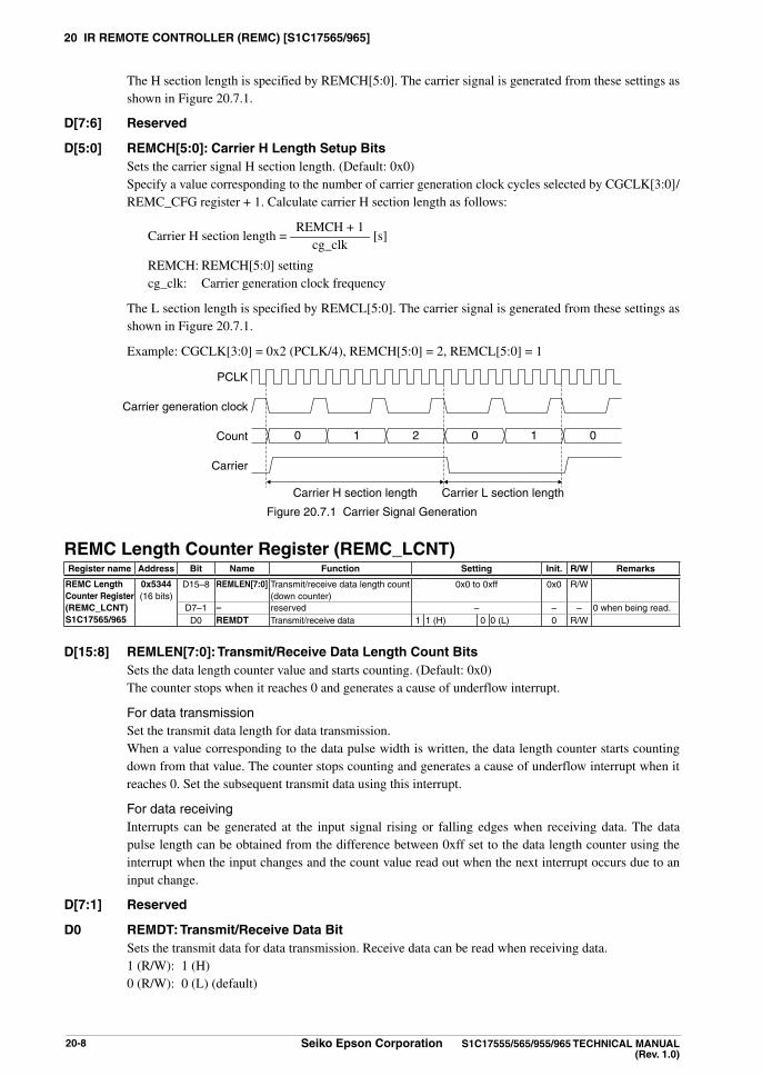
20 iR ReMOTe COnTROlleR (ReMC) [S1C17565/965]
20-8 Seiko epson Corporation S1C17555/565/955/965 TeChniCal Manual (Rev. 1.0)
The H section length is specified by REMCH[5:0]. The carrier signal is generated from these settings as shown in Figure 20.7.1.
D[7:6] Reserved
D[5:0] ReMCh[5:0]: Carrier h length Setup BitsSets the carrier signal H section length. (Default: 0x0)Specify a value corresponding to the number of carrier generation clock cycles selected by CGCLK[3:0]/REMC_CFG register + 1. Calculate carrier H section length as follows:
REMCH + 1Carrier H section length = —————— [s] cg_clk
REMCH: REMCH[5:0] settingcg_clk: Carrier generation clock frequency
The L section length is specified by REMCL[5:0]. The carrier signal is generated from these settings as shown in Figure 20.7.1.
Example: CGCLK[3:0] = 0x2 (PCLK/4), REMCH[5:0] = 2, REMCL[5:0] = 1
PCLK
Carrier generation clock
Count
Carrier
0 1 2 0 1 0
Carrier H section length Carrier L section length
7.1 Carrier Signal GenerationFigure 20.
ReMC length Counter Register (ReMC_lCnT)Register name address Bit name Function Setting init. R/W Remarks
ReMC length Counter Register(ReMC_lCnT)S1C17565/965
0x5344(16 bits)
D15–8 ReMlen[7:0] Transmit/receive data length count(down counter)
0x0 to 0xff 0x0 R/W
D7–1 – reserved – – – 0 when being read.D0 ReMDT Transmit/receive data 1 1 (H) 0 0 (L) 0 R/W
D[15:8] ReMlen[7:0]: Transmit/Receive Data length Count Bits Sets the data length counter value and starts counting. (Default: 0x0) The counter stops when it reaches 0 and generates a cause of underflow interrupt.
For data transmission Set the transmit data length for data transmission. When a value corresponding to the data pulse width is written, the data length counter starts counting
down from that value. The counter stops counting and generates a cause of underflow interrupt when it reaches 0. Set the subsequent transmit data using this interrupt.
For data receiving Interrupts can be generated at the input signal rising or falling edges when receiving data. The data
pulse length can be obtained from the difference between 0xff set to the data length counter using the interrupt when the input changes and the count value read out when the next interrupt occurs due to an input change.
D[7:1] Reserved
D0 ReMDT: Transmit/Receive Data Bit Sets the transmit data for data transmission. Receive data can be read when receiving data. 1 (R/W): 1 (H) 0 (R/W): 0 (L) (default)

20 iR ReMOTe COnTROlleR (ReMC) [S1C17565/965]
S1C17555/565/955/965 TeChniCal Manual Seiko epson Corporation 20-9(Rev. 1.0)
If REMEN/REMC_CFG register is set to 1, the REMDT setting is modulated by the carrier signal for data transmission and output from the REMO pin. For data receiving, this bit is set to the value corre-sponding to the signal level of the data pulse input.
ReMC interrupt Control Register (ReMC_inT)Register name address Bit name Function Setting init. R/W Remarks
ReMC interrupt Control Register(ReMC_inT)S1C17565/965
0x5346(16 bits)
D15–11 – reserved – – – 0 when being read.D10 ReMFiF Falling edge interrupt flag 1 Cause of
interrupt occurred
0 Cause of interrupt not occurred
0 R/W Reset by writing 1.D9 ReMRiF Rising edge interrupt flag 0 R/WD8 ReMuiF Underflow interrupt flag 0 R/W
D7–3 – reserved – – – 0 when being read.D2 ReMFie Falling edge interrupt enable 1 Enable 0 Disable 0 R/WD1 ReMRie Rising edge interrupt enable 1 Enable 0 Disable 0 R/WD0 ReMuie Underflow interrupt enable 1 Enable 0 Disable 0 R/W
This register controls the data length counter underflow, input signal rising edge, and input signal falling edge inter-rupts. The interrupt flag is set to 1 when the data length counter underflows, or when an input signal rising edge or falling edge is detected. If the corresponding interrupt enable bit has been set to 1, the REMC outputs an interrupt request signal to the ITC at the same time. An interrupt will be generated if the ITC and S1C17 Core interrupt con-ditions are met. When an REMC interrupt occurs, check the interrupt flag status in this register to identify the cause of interrupt occurred. If the interrupt enable bit is set to 0, the interrupt is disabled.
notes: • To prevent interrupt recurrences, the REMC module interrupt flag must be reset in the inter-rupt handler routine after an REMC interrupt has occurred.
• To prevent generating unnecessary interrupts, reset the interrupt flag before enabling inter-rupts by the interrupt enable bit.
D[15:11] Reserved
D10 ReMFiF: Falling edge interrupt Flag Bit Indicates the falling edge interrupt cause occurrence status. 1 (R): Cause of interrupt has occurred 0 (R): No cause of interrupt has occurred (default) 1 (W): Flag is reset 0 (W): Ignored
REMFIF is set to 1 at the input signal falling edge. REMFIF is reset to 0 by writing 1.
D9 ReMRiF: Rising edge interrupt Flag Bit Indicates the rising edge interrupt cause occurrence status. 1 (R): Cause of interrupt has occurred 0 (R): No cause of interrupt has occurred (default) 1 (W): Flag is reset 0 (W): Ignored
REMRIF is set to 1 at the input signal rising edge. REMRIF is reset to 0 by writing 1.
D8 ReMuiF: underflow interrupt Flag Bit Indicates the underflow interrupt cause occurrence status. 1 (R): Cause of interrupt has occurred 0 (R): No cause of interrupt has occurred (default) 1 (W): Flag is reset 0 (W): Ignored
REMUIF is set to 1 when a data length counter underflow occurs. REMUIF is reset to 0 by writing 1.
D[7:3] Reserved

20 iR ReMOTe COnTROlleR (ReMC) [S1C17565/965]
20-10 Seiko epson Corporation S1C17555/565/955/965 TeChniCal Manual (Rev. 1.0)
D2 ReMFie: Falling edge interrupt enable Bit Enables or disables input signal falling edge interrupts. 1 (R/W): Interrupt enabled 0 (R/W): Interrupt disabled (default)
D1 ReMRie: Rising edge interrupt enable Bit Enables or disables input signal rising edge interrupts. 1 (R/W): Interrupt enabled 0 (R/W): Interrupt disabled (default)
D0 ReMuie: underflow interrupt enable Bit Enables or disables data length counter underflow interrupts. 1 (R/W): Interrupt enabled 0 (R/W): Interrupt disabled (default)

21 12-BiT a/D COnVeRTeR (aDC12Sa2) [S1C17565/965]
S1C17555/565/955/965 TeChniCal Manual Seiko epson Corporation 21-1(Rev. 1.0)
12-bit A/D Converter (ADC12SA2) 21 [S1C17565/965]
note: The 12-bit A/D converter (ADC12SA2) is unavailable in the S1C17555/955.
aDC12Sa2 Module Overview 21.1 The S1C17565/965 includes a 12-bit A/D converter (ADC12SA2) that converts analog input signals into 12-bit digital values. The following shows the features of the ADC12SA2 module:
• Conversion method Successive approximation type
• Resolution 12 bits
• Input channel Max. 6 channels (Three channels support multi-channel conversion only.)
• A/D conversion clock Max. 2 MHz
• Sampling rate Max. fADC12CLK/20 [sps] (fADC12CLK: A/D conversion clock frequency)
• Analog input voltage range AVSS to AVDD
• Two measurement modes - One-time measurement mode (for single channel or multi-channels) - Continuous measurement mode (for single channel or multi-channels, terminated with software)
• Two conversion trigger sources - Software trigger - T16A2 Ch.3 compare B signal
• The measurement results can be read as 16-bit data in which the 12-bit converted data aligned to left or right.
• Can generate channel group and all channels measurement completion interrupts.
Figure 21.1.1 shows the ADC12SA2 configuration.
Control circuit
BusI/F
Interrupt request
Trigger signal
ADC12SA2
A/D converter
AVDD regulator
Inte
rnal
dat
a bu
s
AIN3AIN4AIN5AIN6AIN7AIN8
VINA ∗1
AVDD ∗2
AVSS
MSCLK
AVDD
ITC
CLG
T16A2 Ch.3
IOSCOSC3
Divider(1/1–1/8)
ADC12CLKGate
CLKEN/ADC12_CLK
*1 VINA is the power supply pin for the internal AVDD regulator.*2 AVDD can be supplied from either an external power supply or the internal regulator.
1.1 ADC12SA2 ConfigurationFigure 21.

21 12-BiT a/D COnVeRTeR (aDC12Sa2) [S1C17565/965]
21-2 Seiko epson Corporation S1C17555/565/955/965 TeChniCal Manual (Rev. 1.0)
note: The ADC12SA2 provides different control registers/bits with the same functions for each chan-nel and they can be distinguished by a channel number in the register/bit names. This chapter explains these registers/bits as one unified by using “x” (3 to 8 in channel units) or “*” (35 = AIN3–5, 6 = AIN6, 7 = AIN7, and 8 = AIN8)
Examples: ADC12_AINxD register AIN3: ADC12_AIN3D register, AIN4: ADC12_AIN4D register, ··· AIN8: ADC12_AIN8D register
IF_A* bit AIN3–5: IF_A35, AIN6: IF_A6, AIN7: IF_A7, AIN8: IF_A8
aDC12Sa2 input Pins21.2 Table 21.2.1 lists the ADC12SA2 input pins.
2.1 List of ADC12SA2 Input PinsTable 21.
Pin name i/O Qty Function
AIN[5:3] * I 3 Analog signal input pins AIN3 (Ch.3) to AIN5 (Ch.5)Input analog signals to be A/D converted.These channels support conversion in three channel units.
AIN[8:6] * I 3 Analog signal input pins AIN6 (Ch.6) to AIN8 (Ch.8)Input analog signals to be A/D converted.These channels support conversion in one channel units.
AVDD – 1 Analog power supply pinSupply an external AVDD voltage to this pin when the AVDD regulator is not used.When the AVDD regulator is used, this pin outputs the AVDD voltage generated by the regulator.
AVSS – 1 Analog GND pin
* The analog input voltage VAIN must be within the range of VSS ≤ VAIN ≤ AVDD.
aDC12Sa2 Settings21.3 Make the following settings before starting measurement by ADC12SA2.(1) Configure the analog power supply.(2) Configure the operating clock (ADC12CLK).(3) Select the trigger source.(4) Select the channels to be measured.(5) Select the measurement mode.(6) Select the measurement result storing mode.(7) Set interrupt conditions (See Section 21.5).
note: Make sure the A/D conversion control circuit is halted (CTLEN/ADC12_CTL0 register = 0 and MSBUSY/ADC12_CTL1 register = 0) before changing the above settings. Changing the settings while the A/D conversion control circuit is operating may cause a malfunction.
analog Power Supply Settings21.3.1
ADC12SA2 operates with the AVDD analog power voltage. AVDD can be generated using the embedded AVDD regulator as well as supplying from outside the IC.For more information on the embedded regulator control, see the “Power Supply” chapter.
Operating Clock Settings21.3.2
The ADC12SA2 module includes a clock source selector, dividers, and a gate circuit for controlling the operation clock (ADC12CLK).

21 12-BiT a/D COnVeRTeR (aDC12Sa2) [S1C17565/965]
S1C17555/565/955/965 TeChniCal Manual Seiko epson Corporation 21-3(Rev. 1.0)
notes: • The operation clock (ADC12CLK) must be supplied before setting ADC12SA2. Otherwise, ADC12SA2 cannot operate normally.
• Do not set the ADC12CLK frequency that exceeds 2 MHz. The ADC12CLK frequency is determined according to the CLKSRC[1:0]/ADC12_CLK register and CLKDIV[2:0]/ADC12_CLK register settings.
Clock source selection Use CLKSRC[1:0] to select the clock source from IOSC, OSC3, and MSCLK (external clock).
3.1 Clock Source SelectionTable 21.
ClKSRC[1:0] Clock source
0x3 MSCLK (external clock)0x2 OSC30x1 Setting prohibited0x0 IOSC
(Default: 0x0)
Clock division ratio selection Use CLKDIV[2:0] to select the division ratio.
3.2 Clock Source Division Ratio SelectionTable 21.
ClKDiV[2:0] Division ratio
0x7–0x5 Reserved0x4 1/60x3 1/80x2 1/40x1 1/20x0 1/1
(Default: 0x0)
Clock enable The clock supply is enabled with CLKEN/ADC12_CLK register. The CLKEN default setting is 0, which stops
the clock. Setting CLKEN to 1 feeds the clock generated as above to the ADC12SA2 circuit. If no ADC12SA2 operation is required, stop the clock to reduce current consumption.
Trigger Selection 21.3.3
Select a trigger source to start measurement using AFETS/ADC12_CTL0 register. Setting AFETS to 0 (default) se-lects software trigger; setting it to 1 selects T16A2 Ch.3.The sampling frequency (fs) is determined by the time between trigger inputs from the selected source (or time from a trigger input until the conversion data is loaded).
Software trigger Writing 1 to SOFTST/ADC12_CTL0 register with software serves as a trigger to start measurement.
16-bit PWM timer (T16a2) Ch.3 The compare B signal of T16A2 Ch.3 is used as a trigger. Since the T16A2 compare B cycle can be pro-
grammed with flexibility, this trigger source is effective when periodic measurements are required. For more information on timer settings, see the “16-bit PWM Timers (T16A2)” chapter.
Measurement Channel Selections21.3.4
Select the channels used for measurement from among the analog input channels. Whether AIN3 to AIN5 are en-abled for measurement or not are selectable in three channel units, and AIN6 to AIN8 are selectable in one chan-nel units using MS_A*/ADC12_CTL1 register. When MS_A* is 0 (default), the channel will be skipped during measurement. Setting MS_A* to 1 will perform measurement in the channel. Measurement will be continuously performed from the lowest to the highest channel number within the channels selected for measurement.
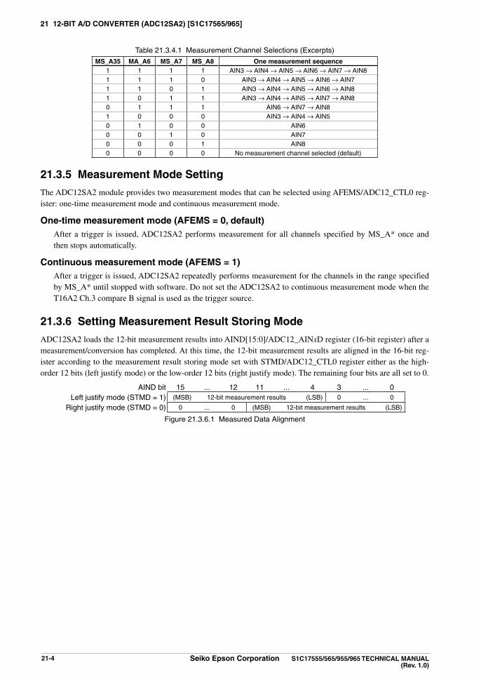
21 12-BiT a/D COnVeRTeR (aDC12Sa2) [S1C17565/965]
21-4 Seiko epson Corporation S1C17555/565/955/965 TeChniCal Manual (Rev. 1.0)
3.4.1 Measurement Channel Selections (Excerpts)Table 21.
MS_a35 Ma_a6 MS_a7 MS_a8 One measurement sequence1 1 1 1 AIN3 → AIN4 → AIN5 → AIN6 → AIN7 → AIN81 1 1 0 AIN3 → AIN4 → AIN5 → AIN6 → AIN71 1 0 1 AIN3 → AIN4 → AIN5 → AIN6 → AIN81 0 1 1 AIN3 → AIN4 → AIN5 → AIN7 → AIN80 1 1 1 AIN6 → AIN7 → AIN81 0 0 0 AIN3 → AIN4 → AIN50 1 0 0 AIN60 0 1 0 AIN70 0 0 1 AIN80 0 0 0 No measurement channel selected (default)
Measurement Mode Setting21.3.5
The ADC12SA2 module provides two measurement modes that can be selected using AFEMS/ADC12_CTL0 reg-ister: one-time measurement mode and continuous measurement mode.
One-time measurement mode (aFeMS = 0, default) After a trigger is issued, ADC12SA2 performs measurement for all channels specified by MS_A* once and
then stops automatically.
Continuous measurement mode (aFeMS = 1) After a trigger is issued, ADC12SA2 repeatedly performs measurement for the channels in the range specified
by MS_A* until stopped with software. Do not set the ADC12SA2 to continuous measurement mode when the T16A2 Ch.3 compare B signal is used as the trigger source.
Setting Measurement Result Storing Mode21.3.6
ADC12SA2 loads the 12-bit measurement results into AIND[15:0]/ADC12_AINxD register (16-bit register) after a measurement/conversion has completed. At this time, the 12-bit measurement results are aligned in the 16-bit reg-ister according to the measurement result storing mode set with STMD/ADC12_CTL0 register either as the high-order 12 bits (left justify mode) or the low-order 12 bits (right justify mode). The remaining four bits are all set to 0.
AIND bit 15 ... 12 11 ... 4 3 ... 0Left justify mode (STMD = 1) (MSB) 12-bit measurement results (LSB) 0 ... 0
Right justify mode (STMD = 0) 0 ... 0 (MSB) 12-bit measurement results (LSB)
3.6.1 Measured Data AlignmentFigure 21.
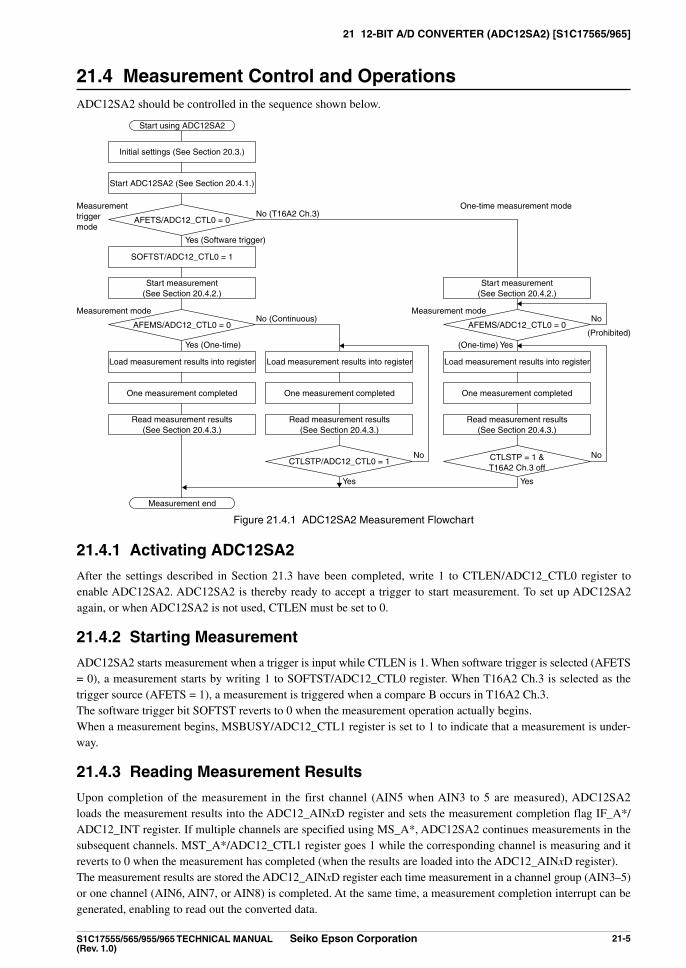
21 12-BiT a/D COnVeRTeR (aDC12Sa2) [S1C17565/965]
S1C17555/565/955/965 TeChniCal Manual Seiko epson Corporation 21-5(Rev. 1.0)
Measurement Control and Operations21.4 ADC12SA2 should be controlled in the sequence shown below.
Start using ADC12SA2
Measurement end
Initial settings (See Section 20.3.)
Start ADC12SA2 (See Section 20.4.1.)
SOFTST/ADC12_CTL0 = 1
Start measurement (See Section 20.4.2.)
Load measurement results into register
One measurement completed
Read measurement results (See Section 20.4.3.)
AFETS/ADC12_CTL0 = 0
Yes (Software trigger)
No (T16A2 Ch.3)Measurement triggermode
One-time measurement mode
AFEMS/ADC12_CTL0 = 0
Yes (One-time) (One-time) Yes
No (Continuous)Measurement mode
Start measurement (See Section 20.4.2.)
AFEMS/ADC12_CTL0 = 0No
(Prohibited)
CTLSTP/ADC12_CTL0 = 1
Yes
No
Measurement mode
Load measurement results into register
One measurement completed
Read measurement results (See Section 20.4.3.)
Load measurement results into register
One measurement completed
Read measurement results (See Section 20.4.3.)
CTLSTP = 1 & T16A2 Ch.3 off
Yes
No
4.1 ADC12SA2 Measurement FlowchartFigure 21.
activating aDC12Sa221.4.1
After the settings described in Section 21.3 have been completed, write 1 to CTLEN/ADC12_CTL0 register to enable ADC12SA2. ADC12SA2 is thereby ready to accept a trigger to start measurement. To set up ADC12SA2 again, or when ADC12SA2 is not used, CTLEN must be set to 0.
Starting Measurement21.4.2
ADC12SA2 starts measurement when a trigger is input while CTLEN is 1. When software trigger is selected (AFETS = 0), a measurement starts by writing 1 to SOFTST/ADC12_CTL0 register. When T16A2 Ch.3 is selected as the trigger source (AFETS = 1), a measurement is triggered when a compare B occurs in T16A2 Ch.3.The software trigger bit SOFTST reverts to 0 when the measurement operation actually begins.When a measurement begins, MSBUSY/ADC12_CTL1 register is set to 1 to indicate that a measurement is under-way.
Reading Measurement Results21.4.3
Upon completion of the measurement in the first channel (AIN5 when AIN3 to 5 are measured), ADC12SA2 loads the measurement results into the ADC12_AINxD register and sets the measurement completion flag IF_A*/ADC12_INT register. If multiple channels are specified using MS_A*, ADC12SA2 continues measurements in the subsequent channels. MST_A*/ADC12_CTL1 register goes 1 while the corresponding channel is measuring and it reverts to 0 when the measurement has completed (when the results are loaded into the ADC12_AINxD register).The measurement results are stored the ADC12_AINxD register each time measurement in a channel group (AIN3–5) or one channel (AIN6, AIN7, or AIN8) is completed. At the same time, a measurement completion interrupt can be generated, enabling to read out the converted data.

21 12-BiT a/D COnVeRTeR (aDC12Sa2) [S1C17565/965]
21-6 Seiko epson Corporation S1C17555/565/955/965 TeChniCal Manual (Rev. 1.0)
If no measurement completion interrupt is used, read the measurement results from the ADC12_AINxD register after confirming that IF_A* is set to 1 indicating completion of measurement. IF_A* is reset to 0 by writing 1.The ADC12_AINxD register is provided for each channel, thus the register is not overwritten in one-time measure-ment mode. In continuous measurement mode, after the first measurement sequence for all the selected channels, the ADC12_AINxD register will be overwritten by the measurement results in the second or following measurement sequences.
Terminating Measurement21.4.4
One-time measurement mode In one-time measurement mode, ADC12SA2 performs measurements of all the channels specified with MS_
A* successively and terminates once the measurements have been completed. To abort measurement, write 1 to CTLSTP/ADC12_CTL0 register. Since the measurement sequence is forcibly terminated, the results of the measurement then underway cannot be obtained.
Continuous execution mode In continuous execution mode, ADC12SA2 repeatedly performs measurements of all the channels specified
with MS_A*. The hardware does not stop the measurement sequence. To stop measurement, write 1 to CTL-STP. Since the measurement sequence is forcibly terminated, the results of the measurement then underway cannot be obtained.
Sampling Rate21.4.5
The sampling rate is determined as “1/ conversion time” by the time between trigger inputs from the selected source (or time from a trigger input until the conversion data is loaded).
The following shows how to determine the conversion time:(1) Measurement circuit startup period *1: 4 * ADC12CLK(2) Measurement circuit operating period: 72 * ADC12CLK(3) A/D conversion period: 20 * ADC12CLK
Conversion time = (1) + (2) + (3) × Number of channels
*1 Required only for the first conversion cycle in continuous measurement mode.
Timing Charts21.4.6
Figure 21.4.6.1 shows the measurement operation timing charts.

21 12-BiT a/D COnVeRTeR (aDC12Sa2) [S1C17565/965]
S1C17555/565/955/965 TeChniCal Manual Seiko epson Corporation 21-7(Rev. 1.0)
(1) Single channel group (ain3–5) one-time measurement mode (MS_a35 = 1, other MS_a* = 0, aFeMS = 0)
CTLEN
Trigger
MSBUSY
Measurement operation
ADC12_AIN3D register
ADC12_AIN4D register
ADC12_AIN5D register
IF_A35
Interrupt request
MeasureAIN3
MeasureAIN4
MeasureAIN5
AIN3 measurement results
AIN4 measurement results
AIN5 measurement results
(2) Multi-channel (ain6, ain7, ain8) one-time measurement mode (MS_a6 = MS_a7 = MS_a8 = 1, other MS_a* = 0, aFeMS = 0)
CTLEN
Trigger
MSBUSY
Measurement operation
ADC12_AIN6D register
ADC12_AIN7D register
ADC12_AIN8D register
IF_A6
IF_A7
IF_A8
Interrupt request
MeasureAIN6
MeasureAIN7
MeasureAIN8
AIN6 measurement results
AIN7 measurement results
AIN8 measurement results
(3) Single channel group (ain3–5) continuous measurement mode (MS_a35 = 1, other MS_a* = 0, aFeMS = 1)
CTLEN
Trigger
CTLSTP
MSBUSY
Measurement operation
ADC12_AIN3D register
ADC12_AIN4D register
ADC12_AIN5D register
IF_A35
Interrupt request
Interrupt reset
MeasureAIN3
MeasureAIN4
MeasureAIN5
Measure
AIN3 measurement results AIN3 measurement results
AIN4 measurement results
AIN5 measurement results
AIN3Measure
AIN4 AIN3 AIN4Measure
AIN5
AIN4 measurement results
AIN5 measurement results

21 12-BiT a/D COnVeRTeR (aDC12Sa2) [S1C17565/965]
21-8 Seiko epson Corporation S1C17555/565/955/965 TeChniCal Manual (Rev. 1.0)
(4) Multi-channel (ain6, ain7, ain8) continuous measurement mode (MS_a6 = MS_a7 = MS_a8 = 1, other MS_a* = 0, aFeMS = 1)
CTLEN
Trigger
CTLSTP
MSBUSY
Measurement operation
ADC12_AIN6D register
ADC12_AIN7D register
ADC12_AIN8D register
IF_A6
IF_A7
IF_A8
Interrupt request
Interrupt reset
MeasureAIN6
MeasureAIN7
MeasureAIN8
AIN6 results
AIN7 measurement results
AIN8 measurement results
MeasureAIN6
MeasureAIN7 AIN6 AIN7
Measure MeasureAIN8
AIN6 measurement results AIN6 measurement results
AIN7 measurement results
AIN8 measurement results
4.6.1 ADC12SA2 OperationsFigure 21.
aDC12Sa2 interrupts 21.5 ADC12SA2 includes a function for generating the following five different types of interrupts.• AIN3–5 completion interrupt • AIN6 completion interrupt• AIN7 completion interrupt • AIN8 completion interrupt• All channels completion interrupt
ADC12SA2 outputs one interrupt signal shared by the five above interrupt causes to the interrupt controller (ITC). Inspect the status flag to determine the interrupt cause occurred.
ain* completion interrupt To use this interrupt, set IEN_A*/ADC12_INT register to 1. If IEN_A* is set to 0 (default), interrupt requests
for this cause will not be sent to the ITC. When measurement in a channel has completed, ADC12SA2 sets IF_A*/ADC12_INT register to 1. If AIN*
completion interrupts are enabled (IEN_A* = 1), an interrupt request is sent simultaneously to the ITC. An in-terrupt occurs if other interrupt conditions are met.
IF_A* is reset to 0 by writing 1.
all channels completion interrupt To use this interrupt, set IEN_ALL/ADC12_INT register to 1. If IEN_ALL is set to 0 (default), interrupt re-
quests for this cause will not be sent to the ITC. When measurements of all the channels selected by MS_A* have completed, ADC12SA2 sets IF_ALL/
ADC12_INT register to 1. If all channels completion interrupts are enabled (IEN_ALL = 1), an interrupt re-quest is sent simultaneously to the ITC. An interrupt occurs if other interrupt conditions are met.
IF_ALL is reset to 0 by writing 1.
For more information on interrupt processing, see the “Interrupt Controller (ITC)” chapter.

21 12-BiT a/D COnVeRTeR (aDC12Sa2) [S1C17565/965]
S1C17555/565/955/965 TeChniCal Manual Seiko epson Corporation 21-9(Rev. 1.0)
notes: • To prevent interrupt recurrences, the interrupt flag must be reset in the interrupt handler rou-tine after an ADC12SA2 interrupt has occurred.
• To prevent unwanted interrupts, reset the interrupt flag before enabling interrupts with the in-terrupt enable bit.
Control Register Details21.6
6.1 List of ADC12SA2 RegistersTable 21.
address Register name Function0x5071 ADC12_CLK ADC12SA2 Clock Control Register Controls ADC12SA2 clock.0x5500 ADC12_CTL0 ADC12SA2 Control Register Controls ADC12SA2.0x5502 ADC12_CTL1 ADC12SA2 Measurement Channel Register Selects measurement channels and indicates the channel status.0x5504 ADC12_INT ADC12SA2 Interrupt Control Register Controls ADC12SA2 interrupts.0x5512 ADC12_AIN3D ADC12SA2 AIN3 Measurement Result Register AIN3 measurement results0x5514 ADC12_AIN4D ADC12SA2 AIN4 Measurement Result Register AIN4 measurement results0x5516 ADC12_AIN5D ADC12SA2 AIN5 Measurement Result Register AIN5 measurement results0x5518 ADC12_AIN6D ADC12SA2 AIN6 Measurement Result Register AIN6 measurement results0x551a ADC12_AIN7D ADC12SA2 AIN7 Measurement Result Register AIN7 measurement results0x551c ADC12_AIN8D ADC12SA2 AIN8 Measurement Result Register AIN8 measurement results
The ADC12SA2 registers are described in detail below.
note: When data is written to the registers, the “Reserved” bits must always be written as 0 and not 1. However, if a value is specified for the “Reserved” bit, do not write a value other than the one that is specified. Furthermore, do not access addresses that are not described in the table above.
aDC12Sa2 Clock Control Register (aDC12_ClK)Register name address Bit name Function Setting init. R/W Remarks
aDC12Sa2 Clock Control Register(aDC12_ClK)S1C17565/965
0x5071(8 bits)
D7 – reserved – – – 0 when being read.D6–4 ClKDiV
[2:0]ADC12SA2 clock division ratio select
CLKDIV[2:0] Division ratio 0x0 R/W0x7–0x5
0x40x30x20x10x0
reserved1/61/81/41/21/1
D3–2 ClKSRC[1:0]
ADC12SA2 clock source select CLKSRC[1:0] Clock source 0x0 R/W0x30x20x10x0
MSCLK (ext)OSC3
reservedIOSC
D1 – reserved – – – 0 when being read.D0 ClKen ADC12SA2 clock enable 1 Enable 0 Disable 0 R/W
D7 Reserved
D[6:4] ClKDiV[2:0]: aDC12Sa2 Clock Division Ratio Select Bits Selects the division ratio for generating the A/D conversion clock (ADC12CLK).
6.2 Clock Source Division Ratio SelectionTable 21.
ClKDiV[2:0] Division ratio
0x7–0x5 Reserved0x4 1/60x3 1/80x2 1/40x1 1/20x0 1/1
(Default: 0x0)

21 12-BiT a/D COnVeRTeR (aDC12Sa2) [S1C17565/965]
21-10 Seiko epson Corporation S1C17555/565/955/965 TeChniCal Manual (Rev. 1.0)
D[3:2] ClKSRC[1:0]: aDC12Sa2 Clock Source Select Bits Selects the clock source.
6.3 Clock Source SelectionTable 21.
ClKSRC[1:0] Clock source
0x3 MSCLK (external clock)0x2 OSC30x1 Setting prohibited0x0 IOSC
(Default: 0x0)
D1 Reserved
D0 ClKen: aDC12Sa2 Clock enable Bit Enables or disables the ADC12CLK supply. 1 (R/W): Enabled (on) 0 (R/W): Disabled (off) (default)
The CLKEN default setting is 0, which disables the clock supply. Setting CLKEN to 1 sends the clock selected to the A/D conversion control circuit.
aDC12Sa2 Control Register (aDC12_CTl0) Register name address Bit name Function Setting init. R/W Remarks
aDC12Sa2 Control Register(aDC12_CTl0)S1C17565/965
0x5500(16 bits)
D15–7 – reserved – – – 0 when being read.D6 STMD Measurement result storing mode 1 AIND[15:4] 0 AIND[11:0] 0 R/WD5 aFeTS Measurement trigger select 1 T16A2 Ch.3 0 Software 0 R/WD4 aFeMS Measurement mode select 1 Continuous 0 Single 0 R/WD3 – reserved – – – 0 when being read.D2 SOFTST Software trigger 1 Start 0 – 0 R/WD1 CTlSTP Measurement termination 1 Stop 0 – 0 R/WD0 CTlen Measurement trigger enable 1 Enable 0 Disable 0 R/W
note: Make sure the A/D conversion control circuit is halted (CTLEN = 0 and MSBUSY/ADC12_CTL1 register = 0) before setting STMD, AFETS, and AFEMS. Changing the settings while the A/D con-version control circuit is operating may cause a malfunction.
D[15:7] Reserved
D6 STMD: Measurement Result Storing Mode Bit Selects the data alignment when the measurement results are loaded into AIND[15:0]/ADC12_AINxD
register. 1 (R/W): Left justify mode (12-bit measurement results → ADD[15:4], ADD[3:0] = 0) 0 (R/W): Right justify mode (12-bit measurement results → ADD[11:0], ADD[15:12] = 0) (default)
D5 aFeTS: Measurement Trigger Select Bit Selects a trigger source to start measurement. 1 (R/W): T16A2 Ch.3 0 (R/W): Software (default)
When 16-bit PWM timer (T16A2) Ch.3 is used, since its compare B signal serves as a trigger, set the compare B cycle and other conditions for the 16-bit PWM timer.
D4 aFeMS: Measurement Mode Select Bit Selects a measurement mode. 1 (R/W): Continuous measurement mode 0 (R/W): One-time measurement mode (default)
Writing 1 to AFEMS sets ADC12SA2 to continuous measurement mode. In this mode, measurements of the channels selected by MS_A*/ADC12_CTL1 register are executed continuously until stopped with software.
When AFEMS is 0, ADC12SA2 operates in one-time measurement mode. In this mode, measurement is terminated after all the channels selected by MS_A* register have been converted once.

21 12-BiT a/D COnVeRTeR (aDC12Sa2) [S1C17565/965]
S1C17555/565/955/965 TeChniCal Manual Seiko epson Corporation 21-11(Rev. 1.0)
note: Do not use continuous measurement mode when the T16A2 Ch.3 compare B signal is used as the trigger.
D3 Reserved
D2 SOFTST: Software Trigger Bit Starts measurement. 1 (W): Software trigger 0 (W): Ignored 1 (R): In measurement start process 0 (R): During measurement/standby (default)
Write 1 to SOFTST to start measurement by a software trigger. SOFTST retains 1 after writing 1 and reverts to 0 when ADC12SA2 actually starts measurement.
No software trigger will be accepted when CTLEN is 0 (ADC12SA2 operation disabled). Writing 0 to SOFTST, writing 1 during measurement, and writing 1 when T16A2 Ch.3 is selected as
the trigger source are ignored.
D1 CTlSTP: Measurement Termination Bit Stops measurement. 1 (W): Force termination 0 (W): Ignored 1 (R): In termination process 0 (R): During measurement/standby (default)
Write 1 to CTLSTP to terminate continuous measurement or to forcibly terminate measurement. CTL-STP retains 1 after writing 1 and reverts to 0 when ADC12SA2 actually terminates the measurement operation. Writing 0 to CTLSTP or writing 1 during standby are ignored.
D0 CTlen: Measurement Trigger enable Bit Enables or disables trigger inputs. 1 (R/W): Enabled 0 (R/W): Disabled (default)
Writing 1 to CTLEN enables ADC12SA2 to start measurement (i.e., ready to accept a trigger). When CTLEN is 0, ADC12SA2 is unable to accept a trigger.
Before setting the modes, measurement channels, or other conditions, be sure to reset CTLEN to 0. This helps to prevent ADC12SA2 from operating erratically.
aDC12Sa2 Measurement Channel Register (aDC12_CTl1) Register name address Bit name Function Setting init. R/W Remarks
aDC12Sa2 Measurement Channel Register(aDC12_CTl1)S1C17565/965
0x5502(16 bits)
D15–13 – reserved – – – 0 when being read.D12 MS_a8 AIN8 measurement enable 1 Enable 0 Disable 0 R/WD11 MS_a7 AIN7 measurement enable 1 Enable 0 Disable 0 R/WD10 MS_a6 AIN6 measurement enable 1 Enable 0 Disable 0 R/WD9 MS_a35 AIN3–5 measurement enable 1 Enable 0 Disable 0 R/W
D8–6 – reserved – – – 0 when being read.D5 MSBuSY Measurement busy status flag 1 Busy 0 Idle 0 RD4 MST_a8 AIN8 measurement status flag 1 Running 0 Standby 0 RD3 MST_a7 AIN7 measurement status flag 1 Running 0 Standby 0 RD2 MST_a6 AIN6 measurement status flag 1 Running 0 Standby 0 RD1 MST_a35 AIN3–5 measurement status flag 1 Running 0 Standby 0 RD0 – reserved – – – 0 when being read.
note: Make sure the A/D conversion control circuit is halted (CTLEN/ADC12_CTL0 register = 0 and MSBUSY = 0) before setting MS_A*. Changing the settings while the A/D conversion control cir-cuit is operating may cause a malfunction.
D[15:13] Reserved
21 12-BiT a/D COnVeRTeR (aDC12Sa2) [S1C17565/965]
21-12 Seiko epson Corporation S1C17555/565/955/965 TeChniCal Manual (Rev. 1.0)
D12 MS_a8: ain8 Measurement enable BitD11 MS_a7: ain7 Measurement enable BitD10 MS_a6: ain6 Measurement enable BitD9 MS_a35: ain3–5 Measurement enable Bit Sets the channels to be measured. 1 (R/W): Measured 0 (R/W): Not measured (default)
D[8:6] Reserved
D5 MSBuSY: Measurement Busy Status Flag Bit Indicates the measurement status. 1 (R): During measurement 0 (R): Measurement completed/standby (default)
MSBUSY is set to 1 when a trigger is issued. In one-time measurement mode, MSBUSY reverts to 0 when the last channel selected by MS_A* is completed and the results are loaded to the ADC12_AINxD register. In continuous measurement mode or when measurement is terminated forcibly, MSBUSY re-verts to 0 when the measurement operation is completed after 1 is written to CTLSTP/ADC12_CTL0 register.
D4 MST_a8: ain8 Measurement Status Flag BitD3 MST_a7: ain7 Measurement Status Flag BitD2 MST_a6: ain6 Measurement Status Flag BitD1 MST_a35: ain3–5 Measurement Status Flag Bit Indicates the measurement status of each channel. 1 (R): During measurement 0 (R): Measurement completed/standby (default)
MST_A* goes 1 when measurement in AIN* begins and reverts to 0 when the measurement is completed and the results are loaded to the ADC12_AIN*D register (ADC12_AIN5D register in the case of MST_A35). When the measurement is terminated forcibly, MST_A* reverts to 0 when ADC-12SA2 terminates the measurement operation.
D0 Reserved
aDC12Sa2 interrupt Control Register (aDC12_inT) Register name address Bit name Function Setting init. R/W Remarks
aDC12Sa2 interrupt Control Register(aDC12_inT)S1C17565/965
0x5504(16 bits)
D15–14 – reserved – – – 0 when being read.D13 iF_all All channels completion int. flag 1 Cause of
interrupt occurred
0 Cause of interrupt not occurred
0 R/W Reset by writing 1.D12 iF_a8 AIN8 completion interrupt flag 0 R/WD11 iF_a7 AIN7 completion interrupt flag 0 R/WD10 iF_a6 AIN6 completion interrupt flag 0 R/WD9 iF_a35 AIN3–5 completion interrupt flag 0 R/W
D8–6 – reserved – – – 0 when being read.D5 ien_all All channels completion int. enable 1 Enable 0 Disable 0 R/WD4 ien_a8 AIN8 completion interrupt enable 1 Enable 0 Disable 0 R/WD3 ien_a7 AIN7 completion interrupt enable 1 Enable 0 Disable 0 R/WD2 ien_a6 AIN6 completion interrupt enable 1 Enable 0 Disable 0 R/WD1 ien_a35 AIN3–5 completion int. enable 1 Enable 0 Disable 0 R/WD0 – reserved – – – 0 when being read.
D[15:14] Reserved
D13 iF_all: all Channels Completion interrupt Flag Bit Indicates the all channels completion interrupt cause occurrence status. 1 (R): Cause of interrupt has occurred 0 (R): No cause of interrupt has occurred (default) 1 (W): Flag is reset 0 (W): Ignored
IF_ALL is set to 1 when a measurement sequence for all the channels selected by MS_A* is completed (when measurement of the last channel is completed and the results are loaded to the ADC12_AINxD register). IF_ALL is reset to 0 by writing 1.

21 12-BiT a/D COnVeRTeR (aDC12Sa2) [S1C17565/965]
S1C17555/565/955/965 TeChniCal Manual Seiko epson Corporation 21-13(Rev. 1.0)
D12 iF_a8: ain8 Completion interrupt Flag BitD11 iF_a7: ain7 Completion interrupt Flag BitD10 iF_a6: ain6 Completion interrupt Flag BitD9 iF_a35: ain3–5 Completion interrupt Flag Bit Indicates the measurement completion interrupt cause occurrence status of each channel. 1 (R): Cause of interrupt has occurred 0 (R): No cause of interrupt has occurred (default) 1 (W): Flag is reset 0 (W): Ignored
IF_A* is set to 1 when measurement in AIN* is completed and the results are loaded to the ADC12_AIN*D register. IF_A* is reset to 0 by writing 1.
D[8:6] Reserved
D5 ien_all: all Channels Completion interrupt enable Bit Enables or disables all channels completion interrupts. 1 (R/W): Interrupt enabled 0 (R/W): Interrupt disabled (default)
D4 ien_a8: ain8 Completion interrupt enable BitD3 ien_a7: ain7 Completion interrupt enable BitD2 ien_a6: ain6 Completion interrupt enable BitD1 ien_a35: ain3–5 Completion interrupt enable Bit Enables or disables the measurement completion interrupt of each channel. 1 (R/W): Interrupt enabled 0 (R/W): Interrupt disabled (default)
D0 Reserved
aDC12Sa2 ainx Measurement Result Registers (aDC12_ainxD) Register name address Bit name Function Setting init. R/W Remarks
aDC12Sa2 ainx Measurement Result Register(aDC12_ainxD)S1C17565/965
0x55120x55140x55160x55180x551a0x551c(16 bits)
D15–0 ainD[15:0] Measurement dataAIND[11:0] are effective when STMD = 0 (AIND[15:12] = 0)AIND[15:4] are effective when STMD = 1 (AIND[3:0] = 0)
0x0 to 0xfff 0x0 R
D[15:0] ainD[15:0]: Measurement Data Bits The measurement results of each channel are stored. (Default: 0x0) Address 0x5512 contains the AIN3 measurement results, ... address 0x551c contains the AIN8 measure-
ment results.
The data alignment in this 16-bit register (measurement result storing mode) can be selected using the STMD/ADC12_CTL0 register.
AIND bit 15 ... 12 11 ... 4 3 ... 0Left justify mode (STMD = 1) (MSB) 12-bit measurement results (LSB) 0 ... 0
Right justify mode (STMD = 0) 0 ... 0 (MSB) 12-bit measurement results (LSB)
6.1 Measured Data AlignmentFigure 21.
This register is a read-only, so writing to this register is ignored.
22 On-ChiP DeBuGGeR (DBG)
S1C17555/565/955/965 TeChniCal Manual Seiko epson Corporation 22-1(Rev. 1.0)
On-chip Debugger (DBG)22
Resource Requirements and Debugging Tools22.1
Debugging work area Debugging requires a 64-byte debugging work area. For more information on the work area location, see the
“Memory Map, Bus Control” chapter. The start address for this debugging work area can be read from the DBRAM register (0xffff90).
Debugging tools Debugging involves connecting ICDmini to the S1C17555/565/955/965 debug pins and inputting the debug in-
struction from the debugger on the personal computer. The following tools are required: • S1C17 Family In-Circuit Debugger ICDmini • S1C17 Family C compiler package (e.g., S5U1C17001C)
Debug pins The following debug pins are used to connect ICDmini.
1.1 List of Debug PinsTable 22.
Pin name i/O Qty Function
DCLK O 1 On-chip debugger clock output pinOutputs a clock to the ICDmini.
DSIO I/O 1 On-chip debugger data input/output pinUsed to input/output debugging data and input the break signal.
DST2 O 1 On-chip debugger status signal output pinOutputs the processor status during debugging.
The on-chip debugger input/output pins (DCLK, DST2, DSIO) are shared with I/O ports and are initially set as the debug pins. If the debugging function is not used, these pins can be switched using the port function select bits to enable use as general-purpose I/O port pins.
For detailed information on pin function switching, see the “I/O Ports (P)” chapter.
Debug Break Operation Status22.2 The S1C17 Core enters debug mode when the brk instruction is executed or a debug interrupt is generated by a break signal (Low) input to the DSIO pin. This state persists until the retd instruction is executed. During this time, hardware interrupts and NMIs are disabled.The default setting halts peripheral circuit operations. This setting can be modified even when debugging is under-way.The peripheral circuits that operate with PCLK will continue running in debug mode by setting PRUND/MISC_PSC register to 1. Setting PRUND to 0 (default) will stop these peripheral circuits in debug mode.The peripheral circuits that operate with a clock other than PCLK will continue running in debug mode by setting DBRUN2/MISC_DMODE2 register to 1. Setting DBRUN2 to 0 (default) will stop these peripheral circuits in de-bug mode.Some peripheral circuits, such as SPI, SPI16, I2CS, T16A2, and ADC12SA2, that run with an external input clock will not stop operating even if the S1C17 Core enters debug mode.

22 On-ChiP DeBuGGeR (DBG)
22-2 Seiko epson Corporation S1C17555/565/955/965 TeChniCal Manual (Rev. 1.0)
additional Debugging Function22.3 The S1C17555/565/955/965 expands the following on-chip debugging functions of the S1C17 Core.
Branching destination in debug mode When a debug interrupt is generated, the S1C17 Core enters debug mode and branches to the debug processing
routine. In this process, the S1C17 Core is designed to branch to address 0xfffc00. In addition to this branch-ing destination, the S1C17555/565/955/965 also allows designation of address 0x0 (beginning address of the internal RAM) as the branching destination when debug mode is activated. The branching destination address is selected using DBADR/MISC_IRAMSZ register. When the DBADR is set to 0 (default), the branching destina-tion is set to 0xfffc00. When it is set to 1, the branching destination is set to 0x0.
adding instruction breaks The S1C17 Core supports two instruction breaks (hardware PC breaks). The S1C17555/565/955/965 increased
this number to five, adding the control bits and registers given below. • IBE2/DCR register: Enables instruction breaks #2. • IBE3/DCR register: Enables instruction breaks #3. • IBE4/DCR register: Enables instruction breaks #4. • IBAR2[23:0]/IBAR2 register: Set instruction break address #2. • IBAR3[23:0]/IBAR3 register: Set instruction break address #3. • IBAR4[23:0]/IBAR4 register: Set instruction break address #4.
Note that the debugger included in the S5U1C17001C (Ver. 1.2.1) or later is required to use five hardware PC breaks.
Control Register Details22.4
4.1 List of Debug RegistersTable 22.
address Register name Function0x4020 MISC_PSC Prescaler Control Register Enables peripheral operations in debug mode (PCLK).0x5322 MISC_DMODE2 Debug Mode Control Register 2 Enables peripheral operations in debug mode (except PCLK).0x5326 MISC_IRAMSZ IRAM Size Select Register Selects the IRAM size.0xffff90 DBRAM Debug RAM Base Register Indicates the debug RAM base address.
0xffffa0 DCR Debug Control Register Controls debugging.
0xffffb8 IBAR2 Instruction Break Address Register 2 Sets Instruction break address #2.
0xffffbc IBAR3 Instruction Break Address Register 3 Sets Instruction break address #3.
0xffffd0 IBAR4 Instruction Break Address Register 4 Sets Instruction break address #4.
The debug registers are described in detail below.
notes: • When data is written to the registers, the “Reserved” bits must always be written as 0 and not 1.
• For debug registers not described here, refer to the S1C17 Core Manual.
Prescaler Control Register (MiSC_PSC)Register name address Bit name Function Setting init. R/W Remarks
Prescaler Control Register(MiSC_PSC)
0x4020(8 bits)
D7–2 – reserved – – – 0 when being read.D1 PRunD Run/stop select in debug mode 1 Run 0 Stop 0 R/WD0 – reserved – – – 0 when being read.
D[7:2] Reserved
D1 PRunD: Run/Stop Select Bit in Debug Mode Selects the operating status of the peripheral circuits that operate with PCLK in debug mode. 1 (R/W): Run 0 (R/W): Stop (default)

22 On-ChiP DeBuGGeR (DBG)
S1C17555/565/955/965 TeChniCal Manual Seiko epson Corporation 22-3(Rev. 1.0)
Setting PRUND to 1 enables the peripheral circuits that operate with PCLK to run even in debug mode. Setting it to 0 will stop them when the S1C17 Core enters debug mode. Set PRUND to 1 to maintain running status for these peripheral circuits in debug mode.
D0 Reserved
Debug Mode Control Register 2 (MiSC_DMODe2)Register name address Bit name Function Setting init. R/W Remarks
Debug Mode Control Register 2(MiSC_DMODe2)
0x5322(16 bits)
D15–1 – reserved – – – 0 when being read.
D0 DBRun2 Run/stop select in debug mode(except PCLK peripheral circuits)
1 Run 0 Stop 0 R/W
D[15:1] Reserved
D0 DBRun2: Run/Stop Select Bit in Debug Mode (except PClK peripheral circuits) Selects the operating status of the peripheral circuits that operate with a clock other than PCLK in debug
mode. 1 (R/W): Run 0 (R/W): Stop (default)
Setting DBRUN2 to 1 enables the peripheral circuits that operate with a clock other than PCLK to run even in debug mode. Setting it to 0 will stop them when the S1C17 Core enters debug mode. Set DBRUN2 to 1 to maintain running status for these peripheral circuits in debug mode.
Some peripheral circuits, such as SPI, SPI16, I2CS, T16A2, and ADC12SA2, that run with an external input clock will not stop operating even if the S1C17 Core enters debug mode.
iRaM Size Select Register (MiSC_iRaMSZ)Register name address Bit name Function Setting init. R/W Remarks
iRaM Size Register(MiSC_iRaMSZ)
0x5326(16 bits)
D15–9 – reserved – – – 0 when being read.D8 DBaDR Debug base address select 1 0x0 0 0xfffc00 0 R/WD7 – reserved – – – 0 when being read.
D6–4 iRaMaCTSZ[2:0]
IRAM actual size 0x2 (= 4KB) 0x2 R
D3 – reserved – – – 0 when being read.D2–0 iRaMSZ[2:0] IRAM size select IRAMSZ[2:0] Size 0x2 R/W
0x7–0x60x50x40x30x2
0x1–0x0
reserved512B1KB2KB4KB
reserved
D[15:9] Reserved
D8 DBaDR: Debug Base address Select Bit Selects the branching destination address when a debug interrupt occurs. 1(R/W): 0x0 0(R/W): 0xfffc00 (default)
D7 Reserved
D[6:4] iRaMaCTSZ[2:0]: iRaM actual Size Bits Indicates the actual internal RAM size embedded. (Default: 0x2)
D3 Reserved
D[2:0] iRaMSZ[2:0]: iRaM Size Select Bits Selects the size of the internal RAM to be used.
22 On-ChiP DeBuGGeR (DBG)
22-4 Seiko epson Corporation S1C17555/565/955/965 TeChniCal Manual (Rev. 1.0)
4.2 Internal RAM Size SelectionTable 22.
iRaMSZ[2:0] internal RaM size
0x7–0x6 Reserved0x5 512B0x4 1KB0x3 2KB0x2 4KB
0x1–0x0 Reserved
(Default: 0x2)
note: The MISC_IRAMSZ register is write-protected. To alter this register settings, you must override this write-protection by writing 0x96 to the MISC_PROT register. Normally, the MISC_PROT reg-ister should be set to a value other than 0x96, except when altering the MISC_IRAMSZ register. Unnecessary rewriting of the MISC_IRAMSZ register may result in system malfunctions.
Debug RaM Base Register (DBRaM)Register name address Bit name Function Setting init. R/W Remarks
Debug RaM Base Register(DBRaM)
0xffff90(32 bits)
D31–24 – Unused (fixed at 0) 0x0 0x0 RD23–0 DBRaM[23:0] Debug RAM base address 0xfc0 0xf
c0R
D[31:24] not used (Fixed at 0)
D[23:0] DBRaM[23:0]: Debug RaM Base address Bits Read-only register containing the beginning address of the debugging work area (64 bytes).
Debug Control Register (DCR)Register name address Bit name Function Setting init. R/W Remarks
Debug ControlRegister(DCR)
0xffffa0(8 bits)
D7 iBe4 Instruction break #4 enable 1 Enable 0 Disable 0 R/WD6 iBe3 Instruction break #3 enable 1 Enable 0 Disable 0 R/WD5 iBe2 Instruction break #2 enable 1 Enable 0 Disable 0 R/WD4 DR Debug request flag 1 Occurred 0 Not occurred 0 R/W Reset by writing 1.D3 iBe1 Instruction break #1 enable 1 Enable 0 Disable 0 R/WD2 iBe0 Instruction break #0 enable 1 Enable 0 Disable 0 R/WD1 Se Single step enable 1 Enable 0 Disable 0 R/WD0 DM Debug mode 1 Debug mode 0 User mode 0 R
D7 iBe4: instruction Break #4 enable Bit Enables or disables instruction break #4. 1 (R/W): Enabled 0 (R/W): Disabled (default)
If this bit is set to 1, the instruction fetch address and the value set in the IBAR4 register are compared. If they match, an instruction break is generated. If this bit is set to 0, no comparison is performed.
D6 iBe3: instruction Break #3 enable Bit Enables or disables instruction break #3. 1 (R/W): Enabled 0 (R/W): Disabled (default)
If this bit is set to 1, the instruction fetch address and the value set in the IBAR3 register are compared. If they match, an instruction break is generated. If this bit is set to 0, no comparison is performed.
D5 iBe2: instruction Break #2 enable Bit Enables or disables instruction break #2. 1 (R/W): Enabled 0 (R/W): Disabled (default)
If this bit is set to 1, the instruction fetch address and the value set in the IBAR2 register are compared. If they match, an instruction break is generated. If this bit is set to 0, no comparison is performed.
D4 DR: Debug Request Flag Bit

22 On-ChiP DeBuGGeR (DBG)
S1C17555/565/955/965 TeChniCal Manual Seiko epson Corporation 22-5(Rev. 1.0)
Indicates the presence or absence of an external debug request. 1 (R): Request generated 0 (R): Request not generated (default) 1 (W): Flag is reset 0 (W): Ignored
This flag is cleared (reset to 0) when 1 is written. It must be cleared before the debug processing routine is terminated by the retd instruction.
D3 iBe1: instruction Break #1 enable Bit Enables or disables instruction break #1. 1 (R/W): Enabled 0 (R/W): Disabled (default)
If this bit is set to 1, the instruction fetch address and the value set in the IBAR1 register are compared. If they match, an instruction break is generated. If this bit is set to 0, no comparison is performed.
D2 iBe0: instruction Break #0 enable Bit Enables or disables instruction break #0. 1 (R/W): Enabled 0 (R/W): Disabled (default)
If this bit is set to 1, the instruction fetch address and the value set in the IBAR0 register are compared. If they match, an instruction break is generated. If this bit is set to 0, no comparison is performed.
D1 Se: Single Step enable Bit Enables or disables single-step operations. 1 (R/W): Enabled 0 (R/W): Disabled (default)
D0 DM: Debug Mode Bit Indicates the processor operating mode (debug mode or user mode). 1 (R): Debug mode 0 (R): User mode (default)
instruction Break address Register 2 (iBaR2)Register name address Bit name Function Setting init. R/W Remarks
instructionBreak addressRegister 2(iBaR2)
0xffffb8(32 bits)
D31–24 – reserved – – – 0 when being read.D23–0 iBaR2[23:0] Instruction break address #2
IBAR223 = MSBIBAR20 = LSB
0x0 to 0xffffff 0x0 R/W
D[31:24] Reserved
D[23:0] iBaR2[23:0]: instruction Break address #2 Bits Sets instruction break address #2. (default: 0x000000)
instruction Break address Register 3 (iBaR3)Register name address Bit name Function Setting init. R/W Remarks
instructionBreak addressRegister 3(iBaR3)
0xffffbc(32 bits)
D31–24 – reserved – – – 0 when being read.D23–0 iBaR3[23:0] Instruction break address #3
IBAR323 = MSBIBAR30 = LSB
0x0 to 0xffffff 0x0 R/W
D[31:24] Reserved
D[23:0] iBaR3[23:0]: instruction Break address #3 Bits Sets instruction break address #3. (default: 0x000000)

22 On-ChiP DeBuGGeR (DBG)
22-6 Seiko epson Corporation S1C17555/565/955/965 TeChniCal Manual (Rev. 1.0)
instruction Break address Register 4 (iBaR4)Register name address Bit name Function Setting init. R/W Remarks
instructionBreak addressRegister 4(iBaR4)
0xffffd0(32 bits)
D31–24 – reserved – – – 0 when being read.D23–0 iBaR4[23:0] Instruction break address #4
IBAR423 = MSBIBAR40 = LSB
0x0 to 0xffffff 0x0 R/W
D[31:24] Reserved
D[23:0] iBaR4[23:0]: instruction Break address #4 Bits Sets instruction break address #4. (default: 0x000000)

23 MulTiPlieR/DiViDeR (COPRO)
S1C17555/565/955/965 TeChniCal Manual Seiko epson Corporation 23-1(Rev. 1.0)
Multiplier/Divider (COPRO)23
Overview23.1 The S1C17555/565/955/965 has an embedded coprocessor that provides multiplier/divider functions.The following shows the features of the multiplier/divider:
• Multiplication: Supports signed/unsigned multiplications. (16 bits × 16 bits = 32 bits) Can be executed in 1 cycle.
• Multiplication and accumulation (MAC): Supports signed MAC operations with overflow detection function. (16 bits × 16 bits + 32 bits = 32 bits) Can be executed in 1 cycle.
• Division: Supports signed/unsigned divisions. (16 bits ÷ 16 bits = 16 bits with 16-bit residue) Can be executed in 17 to 20 cycles.
S1C17 Core
Arithmetic unit
Operation result register
Mode setting
Selector
Argument 2
Argument 1
Coprocessoroutput
Flag output
Operationresult
1.1 Multiplier/Divider Block DiagramFigure 23.
Operation Mode and Output Mode23.2 The Multiplier/divider operates according to the operation mode specified by the application program. As listed in Table 23.2.1, the multiplier/divider supports nine operations.The multiplication, division and MAC results are 32-bit data, therefore, the S1C17 Core cannot read them in one access cycle. The output mode is provided to specify the high-order 16 bits or low-order 16 bits of the operation results to be read from the multiplier/divider.The operation and output modes can be specified with a 7-bit data by writing it to the mode setting register in the multiplier/divider. Use a “ld.cw” instruction for this writing.
ld.cw %rd,%rs %rs[6:0] is written to the mode setting register. (%rd: not used) ld.cw %rd,imm7 imm7[6:0] is written to the mode setting register. (%rd: not used)
6 4 3 0Output mode setting value Operation mode setting value
2.1 Mode Setting RegisterFigure 23.

23 MulTiPlieR/DiViDeR (COPRO)
23-2 Seiko epson Corporation S1C17555/565/955/965 TeChniCal Manual (Rev. 1.0)
2.1 Mode SettingsTable 23.
Setting value (D[6:4])
Output modeSetting value
(D[3:0])Operation mode
0x0 16 low-order bits output modeThe low-order 16 bits of operation results can be read as the coprocessor output.
0x0 initialize mode 0Clears the operation result register to 0x0.
0x1 16 high-order bits output modeThe high-order 16 bits of operation results can be read as the coprocessor output.
0x1 initialize mode 1Loads the 16-bit augend into the low-order 16 bits of the operation result register.
0x2–0x7 Reserved 0x2 initialize mode 2Loads the 32-bit augend into the operation result register.
0x3 Operation result read modeOutputs the data in the operation result reg-ister without computation.
0x4 unsigned multiplication modePerforms unsigned multiplication.
0x5 Signed multiplication modePerforms signed multiplication.
0x6 Reserved0x7 Signed MaC mode
Performs signed MAC operation.0x8 unsigned division mode
Performs unsigned division.0x9 Signed division mode
Performs signed division.0xa–0xf Reserved
Multiplication23.3 The multiplication function performs “A (32 bits) = B (16 bits) × C (16 bits).”To perform a multiplication, set the operation mode to 0x4 (unsigned multiplication) or 0x5 (signed multiplication). Then send the 16-bit multiplicand (B) and 16-bit multiplier (C) to the multiplier/divider using a “ld.ca” instruc-tion. The one-half (16 bits according to the output mode) result (A[15:0] or A[31:16]) and the flag status will be returned to the CPU registers. Another one-half should be read by setting the multiplier/divider into operation result read mode.
S1C17 CoreOperation result
register
Selector
Argument 2
Argument 1 16 bits
32 bits
Coprocessoroutput (16 bits)
Flag output
Operationresult
3.1 Data Path in Multiplication ModeFigure 23.

23 MulTiPlieR/DiViDeR (COPRO)
S1C17555/565/955/965 TeChniCal Manual Seiko epson Corporation 23-3(Rev. 1.0)
3.1 Operation in Multiplication ModeTable 23.
Mode setting value
instruction Operations Flags Remarks
0x04 or 0x05
ld.ca %rd,%rs res[31:0] ← %rd × %rs%rd ← res[15:0]
psr (CVZN) ← 0b0000 The operation result register keeps the operation result until it is rewritten by other opera-tion.
(ext imm9) ld.ca %rd,imm7
res[31:0] ← %rd × imm7/16%rd ← res[15:0]
0x14 or 0x15
ld.ca %rd,%rs res[31:0] ← %rd × %rs %rd ← res[31:16]
(ext imm9) ld.ca %rd,imm7
res[31:0] ← %rd × imm7/16 %rd ← res[31:16]
res: operation result register
Example:ld.cw %r0,0x4 ; Sets the modes (unsigned multiplication mode and 16 low-order bits output mode).ld.ca %r0,%r1 ; Performs “res = %r0 × %r1” and loads the 16 low-order bits of the result to %r0.ld.cw %r0,0x13 ; Sets the modes (operation result read mode and 16 high-order bits output mode).ld.ca %r1,%r0 ; Loads the 16 high-order bits of the result to %r1.
Division23.4 The division function performs “B (16 bits) ÷ C (16 bits) = A (16 bits), residue D (16 bits).”To perform a division, set the operation mode to 0x8 (unsigned division) or 0x9 (signed division). Then send the 16-bit dividend (B) and 16-bit divisor (C) to the multiplier/divider using a “ld.ca” instruction. The quotient and the residue will be stored in the low-order 16 bits and the high-order 16 bits of the operation result register, respec-tively. The 16-bit quotient or residue according to the output mode specification and the flag status will be returned to the CPU registers. Another 16-bit result should be read by setting the multiplier/divider into operation result read mode.
S1C17 CoreOperation result
register
Selector
Argument 2
Argument 1 16 bits
16 bits
Coprocessoroutput (16 bits)
Flag output
Operationresult
÷
4.1 Data Path in Division ModeFigure 23.
4.1 Operation in Division ModeTable 23.
Mode setting value
instruction Operations Flags Remarks
0x08 or 0x09
ld.ca %rd,%rs res[31:0] ← %rd ÷ %rs%rd ← res[15:0] (quotient)
psr (CVZN) ← 0b0000 The operation result register keeps the operation result until it is rewritten by other opera-tion.
(ext imm9) ld.ca %rd,imm7
res[31:0] ← %rd ÷ imm7/16%rd ← res[15:0] (quotient)
0x018 or 0x19
ld.ca %rd,%rs res[31:0] ← %rd ÷ %rs%rd ← res[31:16] (residue)
(ext imm9) ld.ca %rd,imm7
res[31:0] ← %rd ÷ imm7/16%rd ← res[31:16] (residue)
res: operation result register

23 MulTiPlieR/DiViDeR (COPRO)
23-4 Seiko epson Corporation S1C17555/565/955/965 TeChniCal Manual (Rev. 1.0)
Example:ld.cw %r0,0x8 ; Sets the modes (unsigned division mode and 16 low-order bits output mode).ld.ca %r0,%r1 ; Performs “res = %r0 ÷ %r1” and loads the 16 low-order bits of the result (quotient) to %r0.ld.cw %r0,0x13 ; Sets the modes (operation result read mode and 16 high-order bits output mode).ld.ca %r1,%r0 ; Loads the 16 high-order bits of the result (residue) to %r1.
MaC23.5 The MAC (multiplication and accumulation) function performs “A (32 bits) = B (16 bits) × C (16 bits) + A (32 bits).”Before performing a MAC operation, the initial value (A) must be set to the operation result register. To clear the operation result register (A = 0), just set the operation mode to 0x0. It is not necessary to send 0x0 to the multiplier/divider with another instruction.To load a 16-bit value or a 32-bit value to the operation result register, set the operation mode to 0x1 (16 bits) or 0x2 (32 bits), respectively. Then send the initial value to the multiplier/divider using a “ld.cf” instruction.
S1C17 CoreOperation result
register
Selector
Argument 2
Argument 1 16 bits
32 bits
Coprocessoroutput (16 bits)
Flag output
5.1 Data Path in Initialize ModeFigure 23.
5.1 Initializing the Operation Result RegisterTable 23.
Mode setting value
instruction Operations Remarks
0x0 – res[31:0] ← 0x0 Setting the operating mode executes the initialization without sending data.
0x1 ld.cf %rd,%rs res[31:16] ← 0x0 res[15:0] ← %rs
(ext imm9) ld.cf %rd,imm7
res[31:16] ← 0x0 res[15:0] ← imm7/16
0x2 ld.cf %rd,%rs res[31:16] ← %rd res[15:0] ← %rs
(ext imm9) ld.cf %rd,imm7
res[31:16] ← %rd res[15:0] ← imm7/16
res: operation result register
To perform a MAC operation, set the operation mode to 0x7 (signed MAC). Then send the 16-bit multiplicand (B) and 16-bit multiplier (C) to the multiplier/divider using a “ld.ca” instruction. The one-half (16 bits according to the output mode) result (A[15:0] or A[31:16]) and the flag status will be returned to the CPU registers. Another one-half should be read by setting the multiplier/divider into operation result read mode.The overflow (V) flag in the PSR may be set to 1 according to the result. Other flags are set to 0.When repeating the MAC operation without operation result read mode inserted, send multiplicand and multiplier data for number of required times. In this case it is not necessary to set the MAC mode every time.

23 MulTiPlieR/DiViDeR (COPRO)
S1C17555/565/955/965 TeChniCal Manual Seiko epson Corporation 23-5(Rev. 1.0)
S1C17 CoreOperation result
register
Selector
Argument 2
Argument 1 16 bits 32 bits
32 bits
Coprocessoroutput (16 bits)
Flag output
Operationresult
5.2 Data Path in MAC ModeFigure 23.
5.2 Operation in MAC ModeTable 23.
Mode setting value
instruction Operations Flags Remarks
0x07 ld.ca %rd,%rs res[31:0] ← %rd × %rs + res[31:0]%rd ← res[15:0]
psr (CVZN) ← 0b0100 if an overflow has oc-curred
Otherwise psr (CVZN) ← 0b0000
The operation result register keeps the operation result un-til it is rewritten by other operation.
(ext imm9) ld.ca %rd,imm7
res[31:0] ← %rd × imm7/16 + res[31:0]%rd ← res[15:0]
0x17 ld.ca %rd,%rs res[31:0] ← %rd × %rs + res[31:0]%rd ← res[31:16]
(ext imm9) ld.ca %rd,imm7
res[31:0] ← %rd × imm7/16 + res[31:0]%rd ← res[31:16]
res: operation result register
Example:ld.cw %r0,0x7 ; Sets the modes (signed MAC mode and 16 low-order bits output mode).ld.ca %r0,%r1 ; Performs “res = %r0 × %r1 + res” and loads the 16 low-order bits of the result to %r0.ld.cw %r0,0x13 ; Sets the modes (operation result read mode and 16 high-order bits output mode).ld.ca %r1,%r0 ; Loads the 16 high-order bits of the result to %r1.
Conditions to set the overflow (V) flag An overflow occurs in a MAC operation and the overflow (V) flag is set to 1 when the signs of the multiplica-
tion result, operation result register value, and multiplication & accumulation result match the following condi-tions:
5.3 Conditions to Set the Overflow (V) FlagTable 23.
Mode setting value Sign of multiplication resultSign of operation result
register valueSign of multiplication & ac-
cumulation result
0x07 0 (positive) 0 (positive) 1 (negative)0x07 1 (negative) 1 (negative) 0 (positive)
An overflow occurs when a MAC operation performs addition of positive values and a negative value results, or it performs addition of negative values and a positive value results. The coprocessor holds the operation result when the overflow (V) flag is cleared.
Conditions to clear the overflow (V) flag The overflow (V) flag that has been set will be cleared when an overflow has not been occurred during execu-
tion of the “ld.ca” instruction for MAC operation or when the “ld.ca” or “ld.cf” instruction is executed in an operation mode other than operation result read mode.

23 MulTiPlieR/DiViDeR (COPRO)
23-6 Seiko epson Corporation S1C17555/565/955/965 TeChniCal Manual (Rev. 1.0)
Reading Operation Results23.6 The “ld.ca” instruction cannot load a 32-bit operation result to a CPU register, so a multiplication or MAC opera-tion returns the one-half (16 bits according to the output mode) result (A[15:0] or A[31:16]) and the flag status to the CPU registers. Another one-half should be read by setting the multiplier/divider into operation result read mode. The operation result register keeps the loaded operation result until it is rewritten by other operation.
S1C17 CoreOperation result
register
Selector
Argument 2
Argument 1
Coprocessoroutput (16 bits)
Flag output
6.1 Data Path in Operation Result Read ModeFigure 23.
6.1 Operation in Operation Result Read ModeTable 23.
Mode setting value
instruction Operations Flags Remarks
0x03 ld.ca %rd,%rs %rd ← res[15:0] psr (CVZN) ← 0b0000 This operation mode does not affect the operation result reg-ister.
ld.ca %rd,imm7 %rd ← res[15:0]0x13 ld.ca %rd,%rs %rd ← res[31:16]
ld.ca %rd,imm7 %rd ← res[31:16]
res: operation result register

24 FSa [S1C17955/965]
S1C17555/565/955/965 TeChniCal Manual Seiko epson Corporation 24-1(Rev. 1.0)
FSA24 [S1C17955/965]note: FSA is unavailable in the S1C17555/565.
FSA (Flexible Signal Processing Accelerator) is a general-purpose signal processing accelerator that allows pro-grams to configure signal processing flexibly. It has an original instruction set with high code density that provides high-efficiency fixed-point DSP functions.Since FSA loads programs and accesses data independently in contrast to coprocessors, a series of processing, such as FFT, FIR, and IIR filtering, can be executed without using the S1C17 Core power.
Features of FSa
• Harvard architecture (instruction fetch × 1, data read × 2, data write × 1)
• Original instruction architecture with high code density. Multiple operations can be executed in parallel by one instruction.
• Single-cycle multiply and accumulation (Max. 32 × 32 + 72 [bits] → 72 [bits])
• Loop control without overhead
• Conditional instruction execution and conditional loop break
• Circular addressing and bit-reverse addressing
• Hardware saturation calculator
• Auto rounding according to arithmetic right shift count
• Supports multi-channel memory access by multiple memory banks and a bus matrix. Realizes high through-put in the instruction bus and data input/output bus.
FSA_IRQ0FSA_IRQ1 ITC S1C17 Core
Bank 0 (8KB)
Bank 1 (2KB)
Bank 2 (2KB)
32 bits
32 bits
32 bitsFSA
32 bits 32 bits
32 bits
32 bits
32 bits
32 bits
PBUS
XBUS
YBUS
ZBUS
Host-IF
FSACLK
Bus
Mat
rix
Hos
t BusInternal RAM2
1 FSA Configuration Figure 24.
For more information on FSA, please contact a Seiko Epson sales representative.

25 eleCTRiCal ChaRaCTeRiSTiCS
S1C17555/565/955/965 TeChniCal Manual Seiko epson Corporation 25-1(Rev. 1.0)
Electrical Characteristics25
absolute Maximum Ratings25.1 (VSS = 0V)
item Symbol Condition Rated value unitCore power supply voltage LVDD -0.3 to 2.5 *3 VRegulator input voltage VIN *2 -0.3 to 7.0 *3 VI/O power supply voltage HVDD -0.3 to 7.0 VAnalog power supply voltage AVDD -0.3 to 7.0 VFlash programming voltage VPP 8 VInput voltage *1 VI -0.3 to 7.0 VOutput voltage *1 VO -0.3 to 7.0 VHigh level output current IOH 1 pin -10 mA
Total of all pins -20 mALow level output current IOL 1 pin 10 mA
Total of all pins 20 mAStorage temperature Tstg -65 to 125 °C
*1 The rated values of the OSC* pins are the same as those of the core power supply voltage.*2 VINA, VINL, VINP
*3 HVDD ≥ LVDD
Recommended Operating Conditions25.2
S1C17555/955item Symbol Condition Min. Typ. Max. unit
Core power supply voltage LVDD 1.65 1.80 1.95 VI/O power supply voltage HVDD 1.65 – 3.60 VFlash programming voltage VPP 7.30 7.50 7.70 VVPP regulator input voltage VINP VPP regulator output voltage = 7.5V 2.40 – 3.60 VInput voltage (oscillation input pin) LVI OSC1 VSS – LVDD VInput voltage HVI Pxx, #RESET VSS – 3.60 VOperating frequency fOSC1 Crystal oscillation – 32.768 – kHzAmbient temperature Ta During normal operation (Flash read only) -40 – 85 °C
During Flash programming 10 – 40 °C
S1C17565/965item Symbol Condition Min. Typ. Max. unit
Core power supply voltage LVDD When the regulator is not used 1.65 1.80 1.95 VLVDD regulator input voltage VINL REGEN = VINL 2.0 – 3.60 VI/O power supply voltage HVDD 1.65 – 3.60 VAnalog power supply voltage AVDD 2.70 – 3.60 VAVDD regulator input voltage VINA AVDD regulator output voltage = 2.8V 3.10 – 3.60 VFlash programming voltage VPP 7.30 7.50 7.70 VVPP regulator input voltage VINP VPP regulator output voltage = 7.5V 2.40 – 3.60 VInput voltage (oscillation input pin) LVI OSC1, OSC3 VSS – LVDD VInput voltage HVI Pxx, #RESET VSS – 3.60 VOperating frequency fOSC3 Crystal/ceramic oscillation 0.2 – 24 MHz
fOSC1 Crystal oscillation – 32.768 – kHzAmbient temperature Ta During normal operation (Flash read only) -40 – 85 °C
During Flash programming 10 – 40 °C

25 eleCTRiCal ChaRaCTeRiSTiCS
25-2 Seiko epson Corporation S1C17555/565/955/965 TeChniCal Manual (Rev. 1.0)
Current Consumption25.3 Unless otherwise specified: LVDD = 1.8V, HVDD = VINL = AVDD = VINA = VINP = 3.6V, VSS = 0V, Ta = 25°C, PCKEN[1:0] = 0x3 (ON), RDWAIT[1:0] = 0x1 (no wait), CCLKGR[1:0] = 0x0 (gear ratio 1/1), regulator not used
item Symbol Condition Min. Typ. Max. unitCurrent consumptionin SLEEP mode
ISLP OSC1 = OFF, IOSC = OFF, OSC3 = OFF – 1.0 8.2 µA
Current consumptionin HALT mode
IHALT1 OSC1 = 32kHz, IOSC = OFF, OSC3 = OFF, PCKEN[1:0] = 0x0 (OFF)
– 2.9 8.7 µA
OSC1 = 32kHz, IOSC = OFF, OSC3 = OFF – 4.5 10.6 µAIHALT2 *2 OSC1 = 32kHz, IOSC = OFF, OSC3 = 8MHz (ceramic) – 560 650 µA
OSC1 = 32kHz, IOSC = OFF, OSC3 = 24MHz (ceramic) – 1700 2000 µAIHALT3 OSC1 = 32kHz, IOSC = 12MHz, OSC3 = OFF – 1100 1300 µA
Current consumptionin RUN mode *1
IEXE1 OSC1 = 32kHz, IOSC = OFF, OSC3 = OFF, CPU = OSC1 – 15 21 µAOSC1 = 32kHz, IOSC = OFF, OSC3 = OFF, CCLKGR[1:0] = 0x2 (gear ratio 1/4), CPU = OSC1
– 9 14 µA
IEXE2 *2 OSC1 = OFF, IOSC = OFF, OSC3 = 1MHz (ceramic), CPU = OSC3
– 400 510 µA
OSC1 = OFF, IOSC = OFF, OSC3 = 8MHz (ceramic), CPU = OSC3
– 2600 3400 µA
OSC1 = OFF, IOSC = OFF, OSC3 = 24MHz (ceramic), CPU = OSC3, RDWAIT[1:0] = 0x3 (2 wait cycles)
– 4800 6100 µA
OSC1 = OFF, IOSC = OFF, OSC3 = 8MHz (ceramic), CCLKGR[1:0] = 0x2 (gear ratio 1/4), CPU = OSC3
– 1350 1750 µA
IEXE3 OSC1 = OFF, IOSC = 2MHz, OSC3 = OFF, CPU = IOSC – 800 1100 µAOSC1 = OFF, IOSC = 12MHz, OSC3 = OFF, CPU = IOSC – 3500 4600 µA
FSA operating current *3 IEXEF When an FFT computation is performed – 270 350 µA/MHz
*1 The values of current consumption during execution were measured when a test program consisting of 60.5% ALU instructions, 17% branch instructions, 12% memory read instructions, and 10.5% memory write instructions was executed continuously in the Flash memory.
*2 S1C17565/965*3 This current value will be added to the current consumption in Halt/Run mode. This is current consumption per 1MHz of the FSA
operating frequency. Therfore, multiply by the operating frequency (MHz) to determine the actual value (S1C17955/965).
Current consumption-temperature characteristic Current consumption-temperature characteristicin halT mode (OSC1 operation) during execution with OSC1OSC1 = 32.768kHz, IOSC = OFF, OSC3 = OFF, OSC1 = 32.768kHz, IOSC = OFF, OSC3 = OFF, PCKEN[1:0] = 0x0 (OFF), CCLKGR[1:0] = 0x0 (1/1), Typ. value PCKEN[1:0] = 0x3 (ON), CCLKGR[1:0] = 0x0 (1/1), RDWAIT[1:0] = 0x1 (no wait), Typ. value
-50
12
10
8
6
4
2
0-25 0 25 50 75 100
Ta [°C]
IHA
LT1
[µA
]
-50
25
20
15
10
5
0-25 0 25 50 75 100
Ta [°C]
IEX
E1
[µA
]

25 eleCTRiCal ChaRaCTeRiSTiCS
S1C17555/565/955/965 TeChniCal Manual Seiko epson Corporation 25-3(Rev. 1.0)
Current consumption-temperature characteristic Current consumption-temperature characteristicduring execution with OSC3 [S1C17565/965] during execution with iOSCOSC1 = 32.768kHz, IOSC = OFF, OSC3 = 24MHz (ceramic), OSC1 = 32.768kHz, IOSC = 12MHz, OSC3 = OFF, PCKEN[1:0] = 0x3 (ON), CCLKGR[1:0] = 0x0 (1/1), PCKEN[1:0] = 0x3 (ON), CCLKGR[1:0] = 0x0 (1/1),RDWAIT[1:0] = 0x3 (2 wait cycles), Typ. value RDWAIT[1:0] = 0x1 (no wait), Typ. value
-50
5000
4500
4000
3500
3000
2500
2000
1500
1000
500
0-25 0 25 50 75 100
Ta [°C]
IEX
E2
[µA
]
-50
4000
3500
3000
2500
2000
1500
1000
500
0-25 0 25 50 75 100
Ta [°C]IE
XE
3 [µ
A]
Flash read cycle current consumption-frequency Clock gear current consumption-frequency characteristic during execution with OSC3 characteristic during execution with OSC3 [S1C17565/965] [S1C17565/965]OSC1 = 32.768kHz, IOSC = OFF, OSC3 = 24MHz (ceramic), OSC1 = 32.768kHz, IOSC = OFF, OSC3 = ON, PCKEN[1:0] = 0x3 (ON), CCLKGR[1:0] = 0x0 (1/1), PCKEN[1:0] = 0x3 (ON), RDWAIT[1:0] = 0x1 (no wait),Ta = 25°C, Typ. value Ta = 25°C, Typ. value
0 5 10 15 20 25
6000
5000
4000
3000
2000
1000
0
fOSC3 [MHz]
IEX
E2
[µA
] RDWAIT[1:0] = 0x1
RDWAIT[1:0] = 0x2
RDWAIT[1:0] = 0x3
0 5 10 15
4000
3500
3000
2500
2000
1500
1000
500
0
fOSC3 [MHz]
IEX
E2
[µA
]
Gear ratio
1/1
1/2
1/4
1/8
Oscillation Characteristics25.4 Oscillation characteristics change depending on conditions (board pattern, components used, etc.). Use the follow-ing characteristics as reference values.
OSC1 crystal oscillationUnless otherwise specified: LVDD = 1.65 to 1.95V, VSS = 0V, Ta = 25°C, CG1 = CD1 = 10pF external, Rf1 = 10MW external
item Symbol Condition Min. Typ. Max. unitOscillation start time *1 *2 tsta – – 3 s
*1 Crystal resonator = MC-146: manufactured by Seiko Epson (R1 = 65kW Max., CL = 12.5pF)*2 The oscillation start time varies according to the crystal resonator used and the CG1 and CD1 values.
OSC3 crystal oscillation [S1C17565/965]Unless otherwise specified: LVDD = 1.65 to 1.95V, VSS = 0V, Ta = 25°C, CG3 = CD3 = 8pF external, Rf3 = 1MW external
item Symbol Condition Min. Typ. Max. unitOscillation start time *1 *2 tsta – – 20 ms

25 eleCTRiCal ChaRaCTeRiSTiCS
25-4 Seiko epson Corporation S1C17555/565/955/965 TeChniCal Manual (Rev. 1.0)
*1 Crystal resonator = MA-406: manufactured by Seiko Epson (R1 = 150W Max., CL = 10pF)*2 The oscillation start time varies according to the crystal resonator used and the CG3 and CD3 values.
OSC3 ceramic oscillation [S1C17565/965]Unless otherwise specified: LVDD = 1.65 to 1.95V, VSS = 0V, Ta = 25°C, Rf3 = 1MW external
item Symbol Condition Min. Typ. Max. unitOscillation start time *1 *2 tsta – – 1 ms
*1 Ceramic resonator = CSTCG24M0V51: manufactured by Murata Manufacturing Co., Ltd. (CG3 = CD3 = 5pF built-in)*2 The oscillation start time varies according to the ceramic resonator used and the CG3 and CD3 values.
iOSC oscillationUnless otherwise specified: LVDD = 1.8V, VSS = 0V, Ta = 25°C
item Symbol Condition Min. Typ. Max. unitOscillation start time tsta – – 5 µsOscillation frequency fIOSC IOSCSEL[1:0] = 0x3 1.86 2 2.14 MHz
IOSCSEL[1:0] = 0x2 3.76 4 4.24 MHzIOSCSEL[1:0] = 0x0 6.8 8 9.2 MHzIOSCSEL[1:0] = 0x1 11.4 12 12.6 MHz
iOSC oscillation frequency-temperature iOSC oscillation frequency-voltagecharacteristic characteristicTyp. value Typ. value
-50
12 MHz
8 MHz
4 MHz
2 MHz
14
12
10
8
6
4
2
0-25 0 25 50 75 100
Ta [°C]
fIOS
C [M
Hz]
1.6 1.7 1.8 1.9 2.0
12 MHz
8 MHz
4 MHz
2 MHz
14
12
10
8
6
4
2
0
LVDD [V]
fIOS
C [M
Hz]
external Clock input Characteristics25.5
OSC1, OSC3
OSC1
tOSC1H tOSC1L
tOSC3H tOSC3L
tCF1tCR1
VIH
VIL
OSC3
tCF3tCR3
VIH
VIL
Unless otherwise specified: LVDD = 1.65 to 1.95V, VSS = 0V, VIH = 0.8LVDD, VIL = 0.2LVDD, Ta = -40 to 85°C
item Symbol Min. Typ. Max. unitOSC1 input High pulse width tOSC1H 14 – – µsOSC1 input Low pulse width tOSC1L 14 – – µsOSC1 input rise time tCR1 – – 200 nsOSC1 input fall time tCF1 – – 200 nsOSC3 input High pulse width *1 tOSC3H 21 – – nsOSC3 input Low pulse width *1 tOSC3L 21 – – nsOSC3 input rise time *1 tCR3 – – 10 nsOSC3 input fall time *1 tCF3 – – 10 ns
*1 S1C17565/965

25 eleCTRiCal ChaRaCTeRiSTiCS
S1C17555/565/955/965 TeChniCal Manual Seiko epson Corporation 25-5(Rev. 1.0)
eXCl, MSClK, SClKtECH tECL
tCFtCR
VIH
VIL
SCLKx
tCFtCR
VIH
VIL
EXCLx,MSCLK
Unless otherwise specified: HVDD = 1.65 to 3.6V, VSS = 0V, VIH = 0.8HVDD, VIL = 0.2HVDD, Ta = -40 to 85°C
item Symbol Min. Typ. Max. unitEXCLx/MSCLK input High pulse width tECH 21 – – nsEXCLx/MSCLK input Low pulse width tECL 21 – – nsUART transfer rate RU – – 960000 bpsUART transfer rate (IrDA mode) RUIrDA – – 115200 bpsInput rise time tCR – – 80 nsInput fall time tCF – – 80 ns
System Clock Characteristics25.6 Unless otherwise specified: LVDD = 1.65 to 1.95V, VSS = 0V, Ta = -40 to 85°C
item Symbol Condition Min. Typ. Max. unitSystem clock frequency fSYSCLK RDWAIT[1:0] = 0x1 – – 13.5 MHz
RDWAIT[1:0] = 0x2 – – 22.5 MHzRDWAIT[1:0] = 0x3 – – 24 MHz
input/Output Pin Characteristics25.7
Common characteristicsUnless otherwise specified: HVDD = 1.65 to 3.6V, LVDD = 1.65 to 1.95V, VSS = 0V, Ta = -40 to 85°C
item Symbol Condition Min. Typ. Max. unitPin capacitance CIN f = 1MHz, HVDD = 0V – – 8 pFReset low pulse width tSR VIH = 0.8HVDD, VIL = 0.2HVDD 100 – – µsInput leakage current ILI Pxx, #RESET -100 – 100 nA
Unless otherwise specified: HVDD = LVDD = 1.65 to 1.95V, VSS = 0V, Ta = -40 to 85°C
item Symbol Condition Min. Typ. Max. unitHigh level output current IOH VOH = HVDD - 0.4V, HVDD = Min. – – -0.4 mALow level output current IOL VOL = 0.4V, HVDD = Min. 0.4 – – mAPositive trigger voltage VT+ LVCMOS Schmitt 0.66 – 1.36 VNegative trigger voltage VT- LVCMOS Schmitt 0.42 – 1.07 VHysteresis voltage DV LVCMOS Schmitt 0.17 – – VPull-up resistance RPU Type 1, VI = 0V 120 300 1200 kW
Unless otherwise specified: HVDD = 2.2 to 2.6V, LVDD = 1.65 to 1.95V, VSS = 0V, Ta = -40 to 85°C
item Symbol Condition Min. Typ. Max. unitHigh level output current IOH VOH = HVDD - 0.4V, HVDD = Min. – – -0.8 mALow level output current IOL VOL = 0.4V, HVDD = Min. 0.8 – – mAPositive trigger voltage VT+ LVCMOS Schmitt 0.88 – 1.82 VNegative trigger voltage VT- LVCMOS Schmitt 0.55 – 1.43 VHysteresis voltage DV LVCMOS Schmitt 0.22 – – VPull-up resistance RPU Type 1, VI = 0V 60 150 450 kW
Unless otherwise specified: HVDD = 3.0 to 3.6V, LVDD = 1.65 to 1.95V, VSS = 0V, Ta = -40 to 85°C
item Symbol Condition Min. Typ. Max. unitHigh level output current IOH VOH = HVDD - 0.4V, HVDD = Min. – – -1.4 mALow level output current IOL VOL = 0.4V, HVDD = Min. 1.4 – – mAPositive trigger voltage VT+ LVCMOS Schmitt 1.2 – 2.52 VNegative trigger voltage VT- LVCMOS Schmitt 0.75 – 1.98 VHysteresis voltage DV LVCMOS Schmitt 0.3 – – VPull-up resistance RPU Type 1, VI = 0V 32 80 224 kW

25 eleCTRiCal ChaRaCTeRiSTiCS
25-6 Seiko epson Corporation S1C17555/565/955/965 TeChniCal Manual (Rev. 1.0)
Schmitt input threshold voltageHVDD
0VT+VT-0
VIN (V)
VO
UT (
V)
HVDD
Reset pulse
#RESET
tSR
VIH
VIL
SPi/SPi16 Characteristics25.8
SPICLKx(CPOL = 0)
SPICLKx(CPOL = 1)
SDIx
SDOx
tSPCK
tSDO tSDH
tSDS
Master modeUnless otherwise specified: HVDD = 1.65 to 3.6V, VSS = 0V, Ta = -40 to 85°C
item Symbol Min. Typ. Max. unitSPICLKx cycle time tSPCK 250 – – nsSDIx setup time tSDS 70 – – nsSDIx hold time tSDH 10 – – nsSDOx output delay time tSDO – – 20 ns
Slave modeUnless otherwise specified: HVDD = 1.65 to 3.6V, VSS = 0V, Ta = -40 to 85°C
item Symbol Min. Typ. Max. unitSPICLKx cycle time tSPCK 250 – – nsSDIx setup time tSDS 10 – – nsSDIx hold time tSDH 10 – – nsSDOx output delay time tSDO – – 80 ns

25 eleCTRiCal ChaRaCTeRiSTiCS
S1C17555/565/955/965 TeChniCal Manual Seiko epson Corporation 25-7(Rev. 1.0)
i25.9 2C Characteristics
SCLx
SDAx
tSCL
tSTH tSDD tSPH
Unless otherwise specified: HVDD = 1.65 to 3.6V, VSS = 0V, Ta = -40 to 85°C
item Symbol Min. Typ. Max. unitSCL cycle time tSCL 2500 – – nsStart condition hold time tSTH 1/fSYS – – nsData output delay time tSDD 1/fSYS – – nsStop condition hold time tSPH 1/fSYS – – ns
* fSYS: System operating clock frequency
12-bit a/D Converter Characteristics [S1C17565/965]25.10
DC characteristicsUnless otherwise specified: LVDD = 1.65 to 1.95V, AVDD = 2.7 to 3.6V, VSS = 0V, Ta = -40 to 85°C
item Symbol Condition Min. Typ. Max. unitInput pin leakage current ILI VIN = AVSS or AVDD -5 – 5 µADynamic current consumption 1 (VINA power supply)
IDD When the AVDD regulator is usedADC12CLK = 2MHz, measurement of 1ksps × 6ch.
– 90 – µA
Dynamic current consumption 2(AVDD power supply)
IDDA When the AVDD regulator is not usedADC12CLK = 2MHz, measurement of 1ksps × 6ch.
– 30 – µA
Input pin capacitance CIN Pins : AIN3 to AIN8 – – 30 pFAVDD regulator output voltage VAREG Ta = 25°C 2.79 2.8 2.81 VAVDD regulator output temperature coefficient
TCREG Ta = -40 to 85°C – 50 200 ppm/°C
analog characteristicsUnless otherwise specified: LVDD = 1.65 to 1.95V, AVDD = 2.7 to 3.6V, VSS = 0V, Ta = -40 to 85°C
item Symbol Condition Min. Typ. Max. unitA/D resolution – – 12 – bitA/D conversion clock frequency fADC12CLK 250 – 2000 kHzIntegral nonlinearity error EINL – – ±3 LSBDifferential nonlinearity error EDNL – – ±3 LSBFull-scale error EFS -8 – 8 mVZero-scale error EZS -8 – 8 mV
Regulator Characteristics25.11
Regulator current consumptionUnless otherwise specified: Ta = 25°C, No load
item Symbol Condition Min. Typ. Max. unitLVDD regulator current consumption[S1C17565/965]
ILREG1 Economy mode VINL = 2.0 to 3.6V – 0.5 0.8 µAILREG2 Normal mode VINL = 2.0 to 3.6V – 22 33 µA
VPP regulator current consumption IVREG Internal load (2mA) VINP = 2.4 to 3.6V – 8 – mA
Regulator output characteristicsUnless otherwise specified: Ta = -40 to 85°C, No load connected, Input voltage = within the range of the recommended operating condition
item Symbol Condition Min. Typ. Max. unitLVDD regulator output voltage[S1C17565/965]
VLREG 1.65 1.8 1.95 V
VPP regulator output voltage VVREG Ta = 10 to 40°C 7.3 7.5 7.7 V

25 eleCTRiCal ChaRaCTeRiSTiCS
25-8 Seiko epson Corporation S1C17555/565/955/965 TeChniCal Manual (Rev. 1.0)
Flash Memory Characteristics25.12 Unless otherwise specified: LVDD = 1.65 to 1.95V, VPP = 7.5V, VSS = 0V, Ta = 10 to 40°C
item Symbol Condition Min. Typ. Max. unitErase/program count *1 CFEP Programmed data is guaranteed to be retained
for 10 years.40 *2 – – times
*1 Assumed that Erasing + Programming as count of 1. The count includes programming in the factory.*2 Applied only when FLS V1.0 or later is used.

26 BaSiC eXTeRnal COnneCTiOn DiaGRaM
S1C17555/565/955/965 TeChniCal Manual Seiko epson Corporation 26-1(Rev. 1.0)
Basic External Connection Diagram26 S1C17555/955 (when the regulator is not used)
S1C17555/955
R2
CG1
Rf1 X'tal1
CD1
HVDD
R1HVDD
VINP
VPP
C1P
C1N
C1H
C2P
C2N
HVDD
LVDD
#RESET
OSC1
OSC2
VSS
DSIO/P16
DST2/P17
DCLK
Cres
1.65–3.6 V
1.65–1.95 V
Cdsio
CP+
CP+
P00/SDI0
P01/SDO0/SCLM/SCLS
P02/SPICLK0/SDAM/SDAS
P03/#SPISS0
P04/SIN0
P05/SOUT0
P06/SCLK0/FOUTA/#BFR
P07/SCLM/SCLS
P10/SDAM/SDAS
P11/SDI1/TOUTA1/CAPA1
P12(EXCL0)/SDO1
P13(EXCL1)/SPICLK1
P14/#SPISS1/TOUTA0/CAPA0
P15(MSCLK)
DSIO/P16
DST2/P17
P20/SDI2/TOUTA2/CAPA2
P21/SDO2/FOUTB
P22/SPICLK2
P23(EXCL2)/SPISS2
I/O
ICDmini or I/O
ICDmini or Open
[The potential of the substrate (back of the chip) is VSS.]
CO2

26 BaSiC eXTeRnal COnneCTiOn DiaGRaM
26-2 Seiko epson Corporation S1C17555/565/955/965 TeChniCal Manual (Rev. 1.0)
S1C17555/955 (when the regulator is used)
Cf1
CO1
Cf2
CO2
1.65–3.6 V CP+
2.4–3.6 V Ci1Ci2+
S1C17555/955
R2
CG1
Rf1 X'tal1
CD1
[The potential of the substrate (back of the chip) is VSS.]
HVDD
R1HVDD
HVDD
VINP
VPP
LVDD
C1P
C1N
C1H
C2P
C2N
#RESET
OSC1
OSC2
VSS
DSIO/P16
DST2/P17
DCLK
Cres
1.65–1.95 V
Cdsio
CP+
P00/SDI0
P01/SDO0/SCLM/SCLS
P02/SPICLK0/SDAM/SDAS
P03/#SPISS0
P04/SIN0
P05/SOUT0
P06/SCLK0/FOUTA/#BFR
P07/SCLM/SCLS
P10/SDAM/SDAS
P11/SDI1/TOUTA1/CAPA1
P12(EXCL0)/SDO1
P13(EXCL1)/SPICLK1
P14/#SPISS1/TOUTA0/CAPA0
P15(MSCLK)
DSIO/P16
DST2/P17
P20/SDI2/TOUTA2/CAPA2
P21/SDO2/FOUTB
P22/SPICLK2
P23(EXCL2)/SPISS2
I/O
ICDmini or I/O
ICDmini or Open

26 BaSiC eXTeRnal COnneCTiOn DiaGRaM
S1C17555/565/955/965 TeChniCal Manual Seiko epson Corporation 26-3(Rev. 1.0)
S1C17565/965 (when the regulators are not used)
S1C17565/965
R2
CG3
Rf3X'tal3 orCeramic
CD3
HVDD
VINP
VPP
C1P
C1N
C1H
C2P
C2N
VINA
AVDD
HVDD
VINL
REGEN
LVDD
#RESET
OSC1
OSC2
OSC3
OSC4
AVSS
VSS
DSIO/P16
DST2/P17
DCLK
Cres
2.7–3.6 V
1.65–3.6 V
1.65–1.95 V
CP+
CP+
CP+
CG1
Rf1 X'tal1
CD1
ICDmini or I/O
ICDmini or Open
R1HVDD
Cdsio [The potential of the substrate (back of the chip) is VSS.]
AIN3
AIN4
AIN5
AIN6
AIN7
AIN8
ITRS
P00/SDI0
P01/SDO0/SCLM/SCLS
P02/SPICLK0/SDAM/SDAS
P03/#SPISS0
P04/SIN0
P05/SOUT0
P06/SCLK0/FOUTA/#BFR
P07/SCLM/SCLS
P10/SDAM/SDAS
P11/SDI1/TOUTA1/CAPA1
P12(EXCL0)/SDO1
P13(EXCL1)/SPICLK1
P14/#SPISS1/TOUTA0/CAPA0
P15(MSCLK)
DSIO/P16
DST2/P17
P20/SDI2/TOUTA2/CAPA2
P21/SDO2/FOUTB
P22/SPICLK2/REMI
P23(EXCL2)/SPISS2/SCLK1
P24/SIN1/TOUTA3/CAPA3
P25/SOUT1/REMO
P26/SCLM/SCLS
P27/SDAM/SDAS
I/O
General-purposeanalog input
CO2
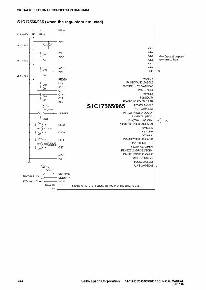
26 BaSiC eXTeRnal COnneCTiOn DiaGRaM
26-4 Seiko epson Corporation S1C17555/565/955/965 TeChniCal Manual (Rev. 1.0)
S1C17565/965 (when the regulators are used)
R2HVDD
ICDmini or I/O
ICDmini or Open
CG3
Rf3X'tal3 orCeramic
CD3
HVDD
VINP
VPP
VINA
AVDD
VINL
REGEN
LVDD
C1P
C1N
C1H
C2P
C2N
#RESET
OSC1
OSC2
OSC3
OSC4
AVSS
VSS
DSIO/P16
DST2/P17
DCLK
Cres
CG1
Rf1 X'tal1
CD1
Cf1
CO1
Cf2
CO4
R1HVDD
Cdsio
CO2
CO3
2.0–3.6 V CP+
2.4–3.6 V
3.1–3.6 V
Ci1Ci2+
Ci3
2.0–3.6 V Ci4
S1C17565/965
[The potential of the substrate (back of the chip) is VSS.]
AIN3
AIN4
AIN5
AIN6
AIN7
AIN8
ITRS
P00/SDI0
P01/SDO0/SCLM/SCLS
P02/SPICLK0/SDAM/SDAS
P03/#SPISS0
P04/SIN0
P05/SOUT0
P06/SCLK0/FOUTA/#BFR
P07/SCLM/SCLS
P10/SDAM/SDAS
P11/SDI1/TOUTA1/CAPA1
P12(EXCL0)/SDO1
P13(EXCL1)/SPICLK1
P14/#SPISS1/TOUTA0/CAPA0
P15(MSCLK)
DSIO/P16
DST2/P17
P20/SDI2/TOUTA2/CAPA2
P21/SDO2/FOUTB
P22/SPICLK2/REMI
P23(EXCL2)/SPISS2/SCLK1
P24/SIN1/TOUTA3/CAPA3
P25/SOUT1/REMO
P26/SCLM/SCLS
P27/SDAM/SDAS
I/O
General-purposeanalog input
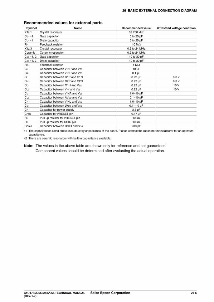
26 BaSiC eXTeRnal COnneCTiOn DiaGRaM
S1C17555/565/955/965 TeChniCal Manual Seiko epson Corporation 26-5(Rev. 1.0)
Recommended values for external partsSymbol name Recommended value Withstand voltage condition
X’tal1 Crystal resonator 32.768 kHzCG1 *1 Gate capacitor 5 to 25 pFCD1 *1 Drain capacitor 5 to 25 pFRf1 Feedback resistor 10 MWX’tal3 Crystal resonator 0.2 to 24 MHzCeramic Ceramic resonator 0.2 to 24 MHzCG3 *1, 2 Gate capacitor 10 to 30 pFCD3 *1, 2 Drain capacitor 10 to 30 pFRf3 Feedback resistor 1 MWCi1 Capacitor between VINP and VSS 10 µFCi2 Capacitor between VINP and VSS 0.1 µFCf1 Capacitor between C1P and C1N 0.22 µF 6.3 VCf2 Capacitor between C2P and C2N 0.22 µF 6.3 VCO1 Capacitor between C1H and VSS 0.22 µF 10 VCO2 Capacitor between VPP and VSS 0.22 µF 10 VCi3 Capacitor between VINA and VSS 1.0–10 µFCO3 Capacitor between AVDD and VSS 0.1–10 µFCi4 Capacitor between VINL and VSS 1.0–10 µFCO4 Capacitor between LVDD and VSS 0.1–1.0 µFCP Capacitor for power supply 3.3 µFCres Capacitor for #RESET pin 0.47 µFR1 Pull-up resistor for #RESET pin 10 kWR2 Pull-up resistor for DSIO pin 10 kWCdsio Capacitor between DSIO and VSS 200 pF
*1 The capacitances listed above include stray capacitance of the board. Please contact the resonator manufacturer for an optimum capacitance.
*2 There are ceramic resonators with built-in capacitance available.
note: The values in the above table are shown only for reference and not guaranteed. Component values should be determined after evaluating the actual operation.

27 PaCKaGe
S1C17555/565/955/965 TeChniCal Manual Seiko epson Corporation 27-1(Rev. 1.0)
Package27 WCSP-48 package (S1C17555/955)
D
ZD
G
F
E
D
C
B
A
1 2 3 4 5 6 7
A1 Corner
Index
A1 Corner
EA
2Z
E2
A1 A
Top View
Bottom View
Sy
φφ
b×
Me
1e
Symbol
DEAA1
A2
e 1e 2bXy
ZD
ZE
Dimension in MillimetersMin–––––––
0.270––––
Nom3.8633.863
–0.260
–0.5000.5000.300
––
0.4320.432
Max––
0.810––––
0.3300.080.05
––

27 PaCKaGe
27-2 Seiko epson Corporation S1C17555/565/955/965 TeChniCal Manual (Rev. 1.0)
TQFP13-64pin package (S1C17565/965)(Unit: mm)
10
12
3348
10 12
17
32
INDEX
0.17–0.27161
64
491
0.11.
2max
1
0.3–0.75
0°–10°
0.09–0.2
0.5

aPPenDiX a liST OF i/O ReGiSTeRS
S1C17555/565/955/965 TeChniCal Manual Seiko epson Corporation aP-a-1(Rev. 1.0)
Appendix A List of I/O Registersinternal peripheral circuit area (0x4000–0x6fff)
Peripheral address Register name FunctionMISC register(8-bit device)
0x4020 MISC_PSC Prescaler Control Register Enables peripheral operations in debug mode (PCLK).
UART (with IrDA) Ch.0(8-bit device)
0x4100 UART_ST0 UART Ch.0 Status Register Indicates transfer, buffer and error statuses.0x4101 UART_TXD0 UART Ch.0 Transmit Data Register Transmit data0x4102 UART_RXD0 UART Ch.0 Receive Data Register Receive data0x4103 UART_MOD0 UART Ch.0 Mode Register Sets transfer data format.0x4104 UART_CTL0 UART Ch.0 Control Register Controls data transfer.0x4105 UART_EXP0 UART Ch.0 Expansion Register Sets IrDA mode.0x4106 UART_BR0 UART Ch.0 Baud Rate Register Sets baud rate.0x4107 UART_FMD0 UART Ch.0 Fine Mode Register Sets fine mode.
UART (with IrDA) Ch.1(8-bit device)S1C17565/965
0x4120 UART_ST1 UART Ch.1 Status Register Indicates transfer, buffer and error statuses.0x4121 UART_TXD1 UART Ch.1 Transmit Data Register Transmit data0x4122 UART_RXD1 UART Ch.1 Receive Data Register Receive data0x4123 UART_MOD1 UART Ch.1 Mode Register Sets transfer data format.0x4124 UART_CTL1 UART Ch.1 Control Register Controls data transfer.0x4125 UART_EXP1 UART Ch.1 Expansion Register Sets IrDA mode.0x4126 UART_BR1 UART Ch.1 Baud Rate Register Sets baud rate.0x4127 UART_FMD1 UART Ch.1 Fine Mode Register Sets fine mode.
Fine mode16-bit timer Ch.0(16-bit device)
0x4200 T16F_CLK0 T16F Ch.0 Count Clock Select Register Selects a count clock.0x4202 T16F_TR0 T16F Ch.0 Reload Data Register Sets reload data.0x4204 T16F_TC0 T16F Ch.0 Counter Data Register Counter data0x4206 T16F_CTL0 T16F Ch.0 Control Register Sets the timer mode and starts/stops the timer.0x4208 T16F_INT0 T16F Ch.0 Interrupt Control Register Controls the interrupt.
16-bit timer Ch.0(16-bit device)
0x4220 T16_CLK0 T16 Ch.0 Count Clock Select Register Selects a count clock.0x4222 T16_TR0 T16 Ch.0 Reload Data Register Sets reload data.0x4224 T16_TC0 T16 Ch.0 Counter Data Register Counter data0x4226 T16_CTL0 T16 Ch.0 Control Register Sets the timer mode and starts/stops the timer.0x4228 T16_INT0 T16 Ch.0 Interrupt Control Register Controls the interrupt.
16-bit timer Ch.1(16-bit device)
0x4240 T16_CLK1 T16 Ch.1 Count Clock Select Register Selects a count clock.0x4242 T16_TR1 T16 Ch.1 Reload Data Register Sets reload data.
0x4244 T16_TC1 T16 Ch.1 Counter Data Register Counter data0x4246 T16_CTL1 T16 Ch.1 Control Register Sets the timer mode and starts/stops the timer.0x4248 T16_INT1 T16 Ch.1 Interrupt Control Register Controls the interrupt.
16-bit timer Ch.2(16-bit device)
0x4260 T16_CLK2 T16 Ch.2 Count Clock Select Register Selects a count clock.0x4262 T16_TR2 T16 Ch.2 Reload Data Register Sets reload data.0x4264 T16_TC2 T16 Ch.2 Counter Data Register Counter data0x4266 T16_CTL2 T16 Ch.2 Control Register Sets the timer mode and starts/stops the timer.0x4268 T16_INT2 T16 Ch.2 Interrupt Control Register Controls the interrupt.
Fine mode16-bit timer Ch.1(16-bit device)
0x4280 T16F_CLK1 T16F Ch.1 Count Clock Select Register Selects a count clock.0x4282 T16F_TR1 T16F Ch.1 Reload Data Register Sets reload data.0x4284 T16F_TC1 T16F Ch.1 Counter Data Register Counter data0x4286 T16F_CTL1 T16F Ch.1 Control Register Sets the timer mode and starts/stops the timer.0x4288 T16F_INT1 T16F Ch.1 Interrupt Control Register Controls the interrupt.
Interrupt controller(16-bit device)
0x4306 ITC_LV0 Interrupt Level Setup Register 0 Sets the P0 and P1 interrupt levels.
0x4308 ITC_LV1 Interrupt Level Setup Register 1 Sets the SWT and CT interrupt levels.
0x430a ITC_LV2 Interrupt Level Setup Register 2 Sets the T16A2 Ch.2 interrupt level.
0x430c ITC_LV3 Interrupt Level Setup Register 3 Sets the SPI16 and T16A2 Ch.0 interrupt levels.
0x430e ITC_LV4 Interrupt Level Setup Register 4 Sets the T16F Ch.0 & Ch.1 and T16 Ch.0 interrupt levels.
0x4310 ITC_LV5 Interrupt Level Setup Register 5 Sets the T16 Ch.1 and T16 Ch.2/T16A2 Ch.3 interrupt levels.
0x4312 ITC_LV6 Interrupt Level Setup Register 6 Sets the UART Ch.0 and Ch.1 interrupt levels.
0x4314 ITC_LV7 Interrupt Level Setup Register 7 Sets the SPI Ch.0 and I2CM interrupt levels.
0x4316 ITC_LV8 Interrupt Level Setup Register 8 Sets the REMC/SPI Ch.1 and T16A2 Ch.1 interrupt levels.
0x4318 ITC_LV9 Interrupt Level Setup Register 9 Sets the ADC12SA2 and FSA (IRQ1) interrupt levels.
0x431a ITC_LV10 Interrupt Level Setup Register 10 Sets the P2 interrupt level.
0x431c ITC_LV11 Interrupt Level Setup Register 11 Sets the I2CS and FSA (IRQ0) interrupt levels.
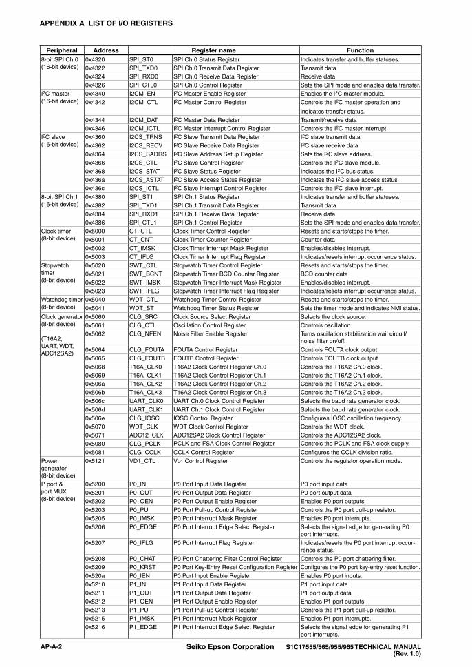
aPPenDiX a liST OF i/O ReGiSTeRS
aP-a-2 Seiko epson Corporation S1C17555/565/955/965 TeChniCal Manual (Rev. 1.0)
Peripheral address Register name Function8-bit SPI Ch.0(16-bit device)
0x4320 SPI_ST0 SPI Ch.0 Status Register Indicates transfer and buffer statuses.0x4322 SPI_TXD0 SPI Ch.0 Transmit Data Register Transmit data0x4324 SPI_RXD0 SPI Ch.0 Receive Data Register Receive data0x4326 SPI_CTL0 SPI Ch.0 Control Register Sets the SPI mode and enables data transfer.
I2C master(16-bit device)
0x4340 I2CM_EN I2C Master Enable Register Enables the I2C master module.0x4342 I2CM_CTL I2C Master Control Register Controls the I2C master operation and
indicates transfer status.0x4344 I2CM_DAT I2C Master Data Register Transmit/receive data0x4346 I2CM_ICTL I2C Master Interrupt Control Register Controls the I2C master interrupt.
I2C slave(16-bit device)
0x4360 I2CS_TRNS I2C Slave Transmit Data Register I2C slave transmit data0x4362 I2CS_RECV I2C Slave Receive Data Register I2C slave receive data0x4364 I2CS_SADRS I2C Slave Address Setup Register Sets the I2C slave address.0x4366 I2CS_CTL I2C Slave Control Register Controls the I2C slave module.0x4368 I2CS_STAT I2C Slave Status Register Indicates the I2C bus status.0x436a I2CS_ASTAT I2C Slave Access Status Register Indicates the I2C slave access status.0x436c I2CS_ICTL I2C Slave Interrupt Control Register Controls the I2C slave interrupt.
8-bit SPI Ch.1(16-bit device)
0x4380 SPI_ST1 SPI Ch.1 Status Register Indicates transfer and buffer statuses.0x4382 SPI_TXD1 SPI Ch.1 Transmit Data Register Transmit data0x4384 SPI_RXD1 SPI Ch.1 Receive Data Register Receive data0x4386 SPI_CTL1 SPI Ch.1 Control Register Sets the SPI mode and enables data transfer.
Clock timer(8-bit device)
0x5000 CT_CTL Clock Timer Control Register Resets and starts/stops the timer.0x5001 CT_CNT Clock Timer Counter Register Counter data0x5002 CT_IMSK Clock Timer Interrupt Mask Register Enables/disables interrupt.0x5003 CT_IFLG Clock Timer Interrupt Flag Register Indicates/resets interrupt occurrence status.
Stopwatch timer(8-bit device)
0x5020 SWT_CTL Stopwatch Timer Control Register Resets and starts/stops the timer.0x5021 SWT_BCNT Stopwatch Timer BCD Counter Register BCD counter data0x5022 SWT_IMSK Stopwatch Timer Interrupt Mask Register Enables/disables interrupt.0x5023 SWT_IFLG Stopwatch Timer Interrupt Flag Register Indicates/resets interrupt occurrence status.
Watchdog timer(8-bit device)
0x5040 WDT_CTL Watchdog Timer Control Register Resets and starts/stops the timer.0x5041 WDT_ST Watchdog Timer Status Register Sets the timer mode and indicates NMI status.
Clock generator(8-bit device)
(T16A2, UART, WDT, ADC12SA2)
0x5060 CLG_SRC Clock Source Select Register Selects the clock source.0x5061 CLG_CTL Oscillation Control Register Controls oscillation.0x5062 CLG_NFEN Noise Filter Enable Register Turns oscillation stabilization wait circuit/
noise filter on/off.0x5064 CLG_FOUTA FOUTA Control Register Controls FOUTA clock output.0x5065 CLG_FOUTB FOUTB Control Register Controls FOUTB clock output.0x5068 T16A_CLK0 T16A2 Clock Control Register Ch.0 Controls the T16A2 Ch.0 clock.0x5069 T16A_CLK1 T16A2 Clock Control Register Ch.1 Controls the T16A2 Ch.1 clock.0x506a T16A_CLK2 T16A2 Clock Control Register Ch.2 Controls the T16A2 Ch.2 clock.0x506b T16A_CLK3 T16A2 Clock Control Register Ch.3 Controls the T16A2 Ch.3 clock.0x506c UART_CLK0 UART Ch.0 Clock Control Register Selects the baud rate generator clock.0x506d UART_CLK1 UART Ch.1 Clock Control Register Selects the baud rate generator clock.0x506e CLG_IOSC IOSC Control Register Configures IOSC oscillation frequency.0x5070 WDT_CLK WDT Clock Control Register Controls the WDT clock.0x5071 ADC12_CLK ADC12SA2 Clock Control Register Controls the ADC12SA2 clock.0x5080 CLG_PCLK PCLK and FSA Clock Control Register Controls the PCLK and FSA clock supply.
0x5081 CLG_CCLK CCLK Control Register Configures the CCLK division ratio.Power generator(8-bit device)
0x5121 VD1_CTL VD1 Control Register Controls the regulator operation mode.
P port & port MUX(8-bit device)
0x5200 P0_IN P0 Port Input Data Register P0 port input data0x5201 P0_OUT P0 Port Output Data Register P0 port output data0x5202 P0_OEN P0 Port Output Enable Register Enables P0 port outputs.0x5203 P0_PU P0 Port Pull-up Control Register Controls the P0 port pull-up resistor.0x5205 P0_IMSK P0 Port Interrupt Mask Register Enables P0 port interrupts.0x5206 P0_EDGE P0 Port Interrupt Edge Select Register Selects the signal edge for generating P0
port interrupts.0x5207 P0_IFLG P0 Port Interrupt Flag Register Indicates/resets the P0 port interrupt occur-
rence status.0x5208 P0_CHAT P0 Port Chattering Filter Control Register Controls the P0 port chattering filter.0x5209 P0_KRST P0 Port Key-Entry Reset Configuration Register Configures the P0 port key-entry reset function.0x520a P0_IEN P0 Port Input Enable Register Enables P0 port inputs.0x5210 P1_IN P1 Port Input Data Register P1 port input data0x5211 P1_OUT P1 Port Output Data Register P1 port output data0x5212 P1_OEN P1 Port Output Enable Register Enables P1 port outputs.0x5213 P1_PU P1 Port Pull-up Control Register Controls the P1 port pull-up resistor.0x5215 P1_IMSK P1 Port Interrupt Mask Register Enables P1 port interrupts.0x5216 P1_EDGE P1 Port Interrupt Edge Select Register Selects the signal edge for generating P1
port interrupts.
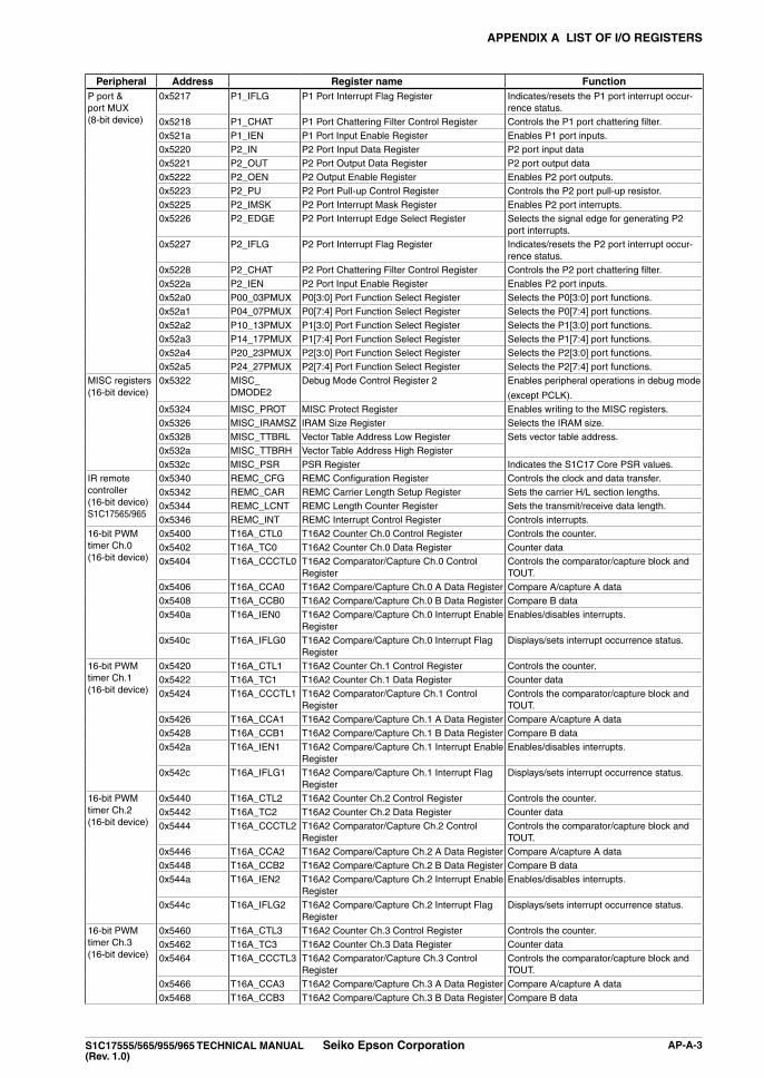
aPPenDiX a liST OF i/O ReGiSTeRS
S1C17555/565/955/965 TeChniCal Manual Seiko epson Corporation aP-a-3(Rev. 1.0)
Peripheral address Register name FunctionP port & port MUX(8-bit device)
0x5217 P1_IFLG P1 Port Interrupt Flag Register Indicates/resets the P1 port interrupt occur-rence status.
0x5218 P1_CHAT P1 Port Chattering Filter Control Register Controls the P1 port chattering filter.0x521a P1_IEN P1 Port Input Enable Register Enables P1 port inputs.0x5220 P2_IN P2 Port Input Data Register P2 port input data0x5221 P2_OUT P2 Port Output Data Register P2 port output data0x5222 P2_OEN P2 Output Enable Register Enables P2 port outputs.0x5223 P2_PU P2 Port Pull-up Control Register Controls the P2 port pull-up resistor.0x5225 P2_IMSK P2 Port Interrupt Mask Register Enables P2 port interrupts.0x5226 P2_EDGE P2 Port Interrupt Edge Select Register Selects the signal edge for generating P2
port interrupts.0x5227 P2_IFLG P2 Port Interrupt Flag Register Indicates/resets the P2 port interrupt occur-
rence status.0x5228 P2_CHAT P2 Port Chattering Filter Control Register Controls the P2 port chattering filter.0x522a P2_IEN P2 Port Input Enable Register Enables P2 port inputs.0x52a0 P00_03PMUX P0[3:0] Port Function Select Register Selects the P0[3:0] port functions.0x52a1 P04_07PMUX P0[7:4] Port Function Select Register Selects the P0[7:4] port functions.0x52a2 P10_13PMUX P1[3:0] Port Function Select Register Selects the P1[3:0] port functions.0x52a3 P14_17PMUX P1[7:4] Port Function Select Register Selects the P1[7:4] port functions.0x52a4 P20_23PMUX P2[3:0] Port Function Select Register Selects the P2[3:0] port functions.0x52a5 P24_27PMUX P2[7:4] Port Function Select Register Selects the P2[7:4] port functions.
MISC registers(16-bit device)
0x5322 MISC_DMODE2
Debug Mode Control Register 2 Enables peripheral operations in debug mode
(except PCLK).0x5324 MISC_PROT MISC Protect Register Enables writing to the MISC registers.0x5326 MISC_IRAMSZ IRAM Size Register Selects the IRAM size.0x5328 MISC_TTBRL Vector Table Address Low Register Sets vector table address.0x532a MISC_TTBRH Vector Table Address High Register0x532c MISC_PSR PSR Register Indicates the S1C17 Core PSR values.
IR remote controller(16-bit device)S1C17565/965
0x5340 REMC_CFG REMC Configuration Register Controls the clock and data transfer.0x5342 REMC_CAR REMC Carrier Length Setup Register Sets the carrier H/L section lengths.0x5344 REMC_LCNT REMC Length Counter Register Sets the transmit/receive data length.0x5346 REMC_INT REMC Interrupt Control Register Controls interrupts.
16-bit PWM timer Ch.0(16-bit device)
0x5400 T16A_CTL0 T16A2 Counter Ch.0 Control Register Controls the counter.0x5402 T16A_TC0 T16A2 Counter Ch.0 Data Register Counter data0x5404 T16A_CCCTL0 T16A2 Comparator/Capture Ch.0 Control
RegisterControls the comparator/capture block and TOUT.
0x5406 T16A_CCA0 T16A2 Compare/Capture Ch.0 A Data Register Compare A/capture A data0x5408 T16A_CCB0 T16A2 Compare/Capture Ch.0 B Data Register Compare B data0x540a T16A_IEN0 T16A2 Compare/Capture Ch.0 Interrupt Enable
RegisterEnables/disables interrupts.
0x540c T16A_IFLG0 T16A2 Compare/Capture Ch.0 Interrupt Flag Register
Displays/sets interrupt occurrence status.
16-bit PWM timer Ch.1(16-bit device)
0x5420 T16A_CTL1 T16A2 Counter Ch.1 Control Register Controls the counter.0x5422 T16A_TC1 T16A2 Counter Ch.1 Data Register Counter data0x5424 T16A_CCCTL1 T16A2 Comparator/Capture Ch.1 Control
RegisterControls the comparator/capture block and TOUT.
0x5426 T16A_CCA1 T16A2 Compare/Capture Ch.1 A Data Register Compare A/capture A data0x5428 T16A_CCB1 T16A2 Compare/Capture Ch.1 B Data Register Compare B data0x542a T16A_IEN1 T16A2 Compare/Capture Ch.1 Interrupt Enable
RegisterEnables/disables interrupts.
0x542c T16A_IFLG1 T16A2 Compare/Capture Ch.1 Interrupt Flag Register
Displays/sets interrupt occurrence status.
16-bit PWM timer Ch.2(16-bit device)
0x5440 T16A_CTL2 T16A2 Counter Ch.2 Control Register Controls the counter.0x5442 T16A_TC2 T16A2 Counter Ch.2 Data Register Counter data0x5444 T16A_CCCTL2 T16A2 Comparator/Capture Ch.2 Control
RegisterControls the comparator/capture block and TOUT.
0x5446 T16A_CCA2 T16A2 Compare/Capture Ch.2 A Data Register Compare A/capture A data0x5448 T16A_CCB2 T16A2 Compare/Capture Ch.2 B Data Register Compare B data0x544a T16A_IEN2 T16A2 Compare/Capture Ch.2 Interrupt Enable
RegisterEnables/disables interrupts.
0x544c T16A_IFLG2 T16A2 Compare/Capture Ch.2 Interrupt Flag Register
Displays/sets interrupt occurrence status.
16-bit PWM timer Ch.3(16-bit device)
0x5460 T16A_CTL3 T16A2 Counter Ch.3 Control Register Controls the counter.0x5462 T16A_TC3 T16A2 Counter Ch.3 Data Register Counter data0x5464 T16A_CCCTL3 T16A2 Comparator/Capture Ch.3 Control
RegisterControls the comparator/capture block and TOUT.
0x5466 T16A_CCA3 T16A2 Compare/Capture Ch.3 A Data Register Compare A/capture A data0x5468 T16A_CCB3 T16A2 Compare/Capture Ch.3 B Data Register Compare B data

aPPenDiX a liST OF i/O ReGiSTeRS
aP-a-4 Seiko epson Corporation S1C17555/565/955/965 TeChniCal Manual (Rev. 1.0)
Peripheral address Register name Function16-bit PWM timer Ch.3(16-bit device)
0x546a T16A_IEN3 T16A2 Compare/Capture Ch.3 Interrupt Enable Register
Enables/disables interrupts.
0x546c T16A_IFLG3 T16A2 Compare/Capture Ch.3 Interrupt Flag Register
Displays/sets interrupt occurrence status.
Flash controller(16-bit device)
0x54b0 FLASHC_WAIT
FLASHC Read Wait Control Register Sets Flash read wait cycle.
12-bit A/D converter(16-bit device)S1C17565/965
0x5500 ADC12_CTL0 ADC12SA2 Control Register Controls ADC12SA2.0x5502 ADC12_CTL1 ADC12SA2 Measurement Channel Register Selects measurement channels and indicates
the channel status.0x5504 ADC12_INT ADC12SA2 Interrupt Control Register Controls ADC12SA2 interrupts.0x550a ADC12_ACTL ADC12SA2 Power Control Register Controls the ADC12SA2 power supply.0x5512 ADC12_AIN3D ADC12SA2 AIN3 Measurement Result Register AIN3 measurement results0x5514 ADC12_AIN4D ADC12SA2 AIN4 Measurement Result Register AIN4 measurement results0x5516 ADC12_AIN5D ADC12SA2 AIN5 Measurement Result Register AIN5 measurement results0x5518 ADC12_AIN6D ADC12SA2 AIN6 Measurement Result Register AIN6 measurement results0x551a ADC12_AIN7D ADC12SA2 AIN7 Measurement Result Register AIN7 measurement results0x551c ADC12_AIN8D ADC12SA2 AIN8 Measurement Result Register AIN8 measurement results
8-bit SPI Ch.1(16-bit device)
0x6040 SPI16_RXD SPI16 Receive Data Register Receive data0x6044 SPI16_TXD SPI16 Transmit Data Register Transmit data0x6048 SPI16_CTL1 SPI16 Control Register 1 Sets modes and enables data transfer.0x604c SPI16_CTL2 SPI16 Control Register 2 Controls slave select input.0x6050 SPI16_WAIT SPI16 Wait Register Sets data transfer wait time.0x6054 SPI16_STAT SPI16 Status Register Indicates transfer and buffer statuses.0x6058 SPI16_INT SPI16 Interrupt Control Register Sets interrupts.0x605c SPI16_RXMK SPI16 Receive Data Mask Register Sets receive data mask.
Core i/O Reserved area (0xffff84–0xffffd0)Peripheral address Register name Function
S1C17 Core I/O 0xffff84 IDIR Processor ID Register Indicates the processor ID.0xffff90 DBRAM Debug RAM Base Register Indicates the debug RAM base address.0xffffa0 DCR Debug Control Register Controls debugging.0xffffb4 IBAR1 Instruction Break Address Register 1 Sets Instruction break address #1.0xffffb8 IBAR2 Instruction Break Address Register 2 Sets Instruction break address #2.0xffffbc IBAR3 Instruction Break Address Register 3 Sets Instruction break address #3.0xffffd0 IBAR4 Instruction Break Address Register 4 Sets Instruction break address #4.
note: Addresses marked as “Reserved” or unused peripheral circuit areas not marked in the table must not be accessed by application programs.
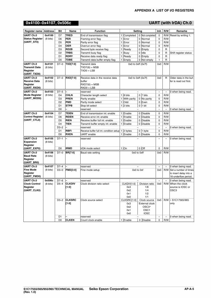
aPPenDiX a liST OF i/O ReGiSTeRS
S1C17555/565/955/965 TeChniCal Manual Seiko epson Corporation aP-a-5(Rev. 1.0)
0x4100–0x4107, 0x506c uaRT (with irDa) Ch.0
Register name address Bit name Function Setting init. R/W Remarks
uaRT Ch.0 Status Register(uaRT_ST0)
0x4100(8 bits)
D7 TReD End of transmission flag 1 Completed 0 Not completed 0 R/W Reset by writing 1.D6 FeR Framing error flag 1 Error 0 Normal 0 R/WD5 PeR Parity error flag 1 Error 0 Normal 0 R/WD4 OeR Overrun error flag 1 Error 0 Normal 0 R/WD3 RD2B Second byte receive flag 1 Ready 0 Empty 0 RD2 TRBS Transmit busy flag 1 Busy 0 Idle 0 R Shift register statusD1 RDRY Receive data ready flag 1 Ready 0 Empty 0 RD0 TDBe Transmit data buffer empty flag 1 Empty 0 Not empty 1 R
uaRT Ch.0 Transmit Data Register(uaRT_TXD0)
0x4101(8 bits)
D7–0 TXD[7:0] Transmit dataTXD7(6) = MSBTXD0 = LSB
0x0 to 0xff (0x7f) 0x0 R/W
uaRT Ch.0 Receive Data Register(uaRT_RXD0)
0x4102(8 bits)
D7–0 RXD[7:0] Receive data in the receive data bufferRXD7(6) = MSBRXD0 = LSB
0x0 to 0xff (0x7f) 0x0 R Older data in the buf-fer is read out first.
uaRT Ch.0 Mode Register(uaRT_MOD0)
0x4103(8 bits)
D7–5 – reserved – – – 0 when being read.D4 Chln Character length select 1 8 bits 0 7 bits 0 R/WD3 PRen Parity enable 1 With parity 0 No parity 0 R/WD2 PMD Parity mode select 1 Odd 0 Even 0 R/WD1 STPB Stop bit select 1 2 bits 0 1 bit 0 R/WD0 – reserved – – – 0 when being read.
uaRT Ch.0 Control Register(uaRT_CTl0)
0x4104(8 bits)
D7 Teien End of transmission int. enable 1 Enable 0 Disable 0 R/WD6 Reien Receive error int. enable 1 Enable 0 Disable 0 R/WD5 Rien Receive buffer full int. enable 1 Enable 0 Disable 0 R/WD4 Tien Transmit buffer empty int. enable 1 Enable 0 Disable 0 R/W
D3–2 – reserved – – – 0 when being read.D1 RBFi Receive buffer full int. condition setup 1 2 bytes 0 1 byte 0 R/WD0 RXen UART enable 1 Enable 0 Disable 0 R/W
uaRT Ch.0expansion Register(uaRT_eXP0)
0x4105(8 bits)
D7–1 – reserved – – – 0 when being read.
D0 iRMD IrDA mode select 1 On 0 Off 0 R/W
uaRT Ch.0Baud Rate Register(uaRT_BR0)
0x4106(8 bits)
D7–0 BR[7:0] Baud rate setting 0x0 to 0xff 0x0 R/W
uaRT Ch.0 Fine Mode Register(uaRT_FMD0)
0x4107(8 bits)
D7–4 – reserved – – – 0 when being read.D3–0 FMD[3:0] Fine mode setup 0x0 to 0xf 0x0 R/W Set a number of times
to insert delay into a 16-underflow period.
uaRT Ch.0 Clock Control Register(uaRT_ClK0)
0x506c(8 bits)
D7–6 – reserved – – – 0 when being read.D5–4 ClKDiV
[1:0]Clock division ratio select CLKDIV[1:0] Division ratio 0x0 R/W When the clock
source is IOSC or OSC3
0x30x20x10x0
1/81/41/21/1
D3–2 ClKSRC[1:0]
Clock source select CLKSRC[1:0] Clock source 0x0 R/W * S1C17565/965 only0x3
0x20x10x0
External clockOSC3*OSC1IOSC
D1 – reserved – – – 0 when being read.D0 ClKen Count clock enable 1 Enable 0 Disable 0 R/W

aPPenDiX a liST OF i/O ReGiSTeRS
aP-a-6 Seiko epson Corporation S1C17555/565/955/965 TeChniCal Manual (Rev. 1.0)
0x4120–0x4127, 0x506d uaRT (with irDa) Ch.1
Register name address Bit name Function Setting init. R/W Remarks
uaRT Ch.1 Status Register(uaRT_ST1)S1C17565/965
0x4120(8 bits)
D7 TReD End of transmission flag 1 Completed 0 Not completed 0 R/W Reset by writing 1.D6 FeR Framing error flag 1 Error 0 Normal 0 R/WD5 PeR Parity error flag 1 Error 0 Normal 0 R/WD4 OeR Overrun error flag 1 Error 0 Normal 0 R/WD3 RD2B Second byte receive flag 1 Ready 0 Empty 0 RD2 TRBS Transmit busy flag 1 Busy 0 Idle 0 R Shift register statusD1 RDRY Receive data ready flag 1 Ready 0 Empty 0 RD0 TDBe Transmit data buffer empty flag 1 Empty 0 Not empty 1 R
uaRT Ch.1 Transmit Data Register(uaRT_TXD1)S1C17565/965
0x4121(8 bits)
D7–0 TXD[7:0] Transmit dataTXD7(6) = MSBTXD0 = LSB
0x0 to 0xff (0x7f) 0x0 R/W
uaRT Ch.1 Receive Data Register(uaRT_RXD1)S1C17565/965
0x4122(8 bits)
D7–0 RXD[7:0] Receive data in the receive data bufferRXD7(6) = MSBRXD0 = LSB
0x0 to 0xff (0x7f) 0x0 R Older data in the buf-fer is read out first.
uaRT Ch.1 Mode Register(uaRT_MOD1)S1C17565/965
0x4123(8 bits)
D7–5 – reserved – – – 0 when being read.D4 Chln Character length select 1 8 bits 0 7 bits 0 R/WD3 PRen Parity enable 1 With parity 0 No parity 0 R/WD2 PMD Parity mode select 1 Odd 0 Even 0 R/WD1 STPB Stop bit select 1 2 bits 0 1 bit 0 R/WD0 – reserved – – – 0 when being read.
uaRT Ch.1 Control Register(uaRT_CTl1)S1C17565/965
0x4124(8 bits)
D7 Teien End of transmission int. enable 1 Enable 0 Disable 0 R/WD6 Reien Receive error int. enable 1 Enable 0 Disable 0 R/WD5 Rien Receive buffer full int. enable 1 Enable 0 Disable 0 R/WD4 Tien Transmit buffer empty int. enable 1 Enable 0 Disable 0 R/W
D3–2 – reserved – – – 0 when being read.D1 RBFi Receive buffer full int. condition setup 1 2 bytes 0 1 byte 0 R/WD0 RXen UART enable 1 Enable 0 Disable 0 R/W
uaRT Ch.1expansion Register(uaRT_eXP1)S1C17565/965
0x4125(8 bits)
D7–1 – reserved – – – 0 when being read.
D0 iRMD IrDA mode select 1 On 0 Off 0 R/W
uaRT Ch.1Baud Rate Register(uaRT_BR1)S1C17565/965
0x4126(8 bits)
D7–0 BR[7:0] Baud rate setting 0x0 to 0xff 0x0 R/W
uaRT Ch.1 Fine Mode Register(uaRT_FMD1)S1C17565/965
0x4127(8 bits)
D7–4 – reserved – – – 0 when being read.D3–0 FMD[3:0] Fine mode setup 0x0 to 0xf 0x0 R/W Set a number of times
to insert delay into a 16-underflow period.
uaRT Ch.1 Clock Control Register(uaRT_ClK1)S1C17565/965
0x506d(8 bits)
D7–6 – reserved – – – 0 when being read.D5–4 ClKDiV
[1:0]Clock division ratio select CLKDIV[1:0] Division ratio 0x0 R/W When the clock
source is IOSC or OSC3
0x30x20x10x0
1/81/41/21/1
D3–2 ClKSRC[1:0]
Clock source select CLKSRC[1:0] Clock source 0x0 R/W0x30x20x10x0
External clockOSC3OSC1IOSC
D1 – reserved – – – 0 when being read.D0 ClKen Count clock enable 1 Enable 0 Disable 0 R/W

aPPenDiX a liST OF i/O ReGiSTeRS
S1C17555/565/955/965 TeChniCal Manual Seiko epson Corporation aP-a-7(Rev. 1.0)
0x4200–0x4208 Fine Mode 16-bit Timer Ch.0
Register name address Bit name Function Setting init. R/W Remarks
T16F Ch.0 Count Clock Select Register(T16F_ClK0)
0x4200(16 bits)
D15–4 – reserved – – – 0 when being read.D3–0 DF[3:0] Count clock division ratio select DF[3:0] Division ratio 0x0 R/W Source clock = PCLK
0xf0xe0xd0xc0xb0xa0x90x80x70x60x50x40x30x20x10x0
reserved1/163841/81921/40961/20481/10241/5121/2561/1281/641/321/161/81/41/21/1
T16F Ch.0 Reload Data Register(T16F_TR0)
0x4202(16 bits)
D15–0 TR[15:0] Reload dataTR15 = MSBTR0 = LSB
0x0 to 0xffff 0x0 R/W
T16F Ch.0 Counter Data Register(T16F_TC0)
0x4204(16 bits)
D15–0 TC[15:0] Counter dataTC15 = MSBTC0 = LSB
0x0 to 0xffff 0xffff R
T16F Ch.0 Control Register(T16F_CT0)
0x4206(16 bits)
D15–12 – reserved – – – 0 when being read.D11–8 TFMD[3:0] Fine mode setup 0x0 to 0xf 0x0 R/W Set a number of times
to insert delay into a 16-underflow period.
D7–5 – reserved – – – 0 when being read.D4 TRMD Count mode select 1 One shot 0 Repeat 0 R/W
D3–2 – reserved – – – 0 when being read.D1 PReSeR Timer reset 1 Reset 0 Ignored 0 WD0 PRun Timer run/stop control 1 Run 0 Stop 0 R/W
T16F Ch.0 interrupt Control Register(T16F_inT0)
0x4208(16 bits)
D15–9 – reserved – – – 0 when being read.D8 T16Fie T16F interrupt enable 1 Enable 0 Disable 0 R/W
D7–1 – reserved – – – 0 when being read.D0 T16FiF T16F interrupt flag 1 Cause of
interrupt occurred
0 Cause of interrupt not occurred
0 R/W Reset by writing 1.
0x4220–0x4228 16-bit Timer Ch.0
Register name address Bit name Function Setting init. R/W Remarks
T16 Ch.0 Count Clock Select Register(T16_ClK0)
0x4220(16 bits)
D15–4 – reserved – – – 0 when being read.D3–0 DF[3:0] Count clock division ratio select DF[3:0] Division ratio 0x0 R/W Source clock = PCLK
0xf0xe0xd0xc0xb0xa0x90x80x70x60x50x40x30x20x10x0
reserved1/163841/81921/40961/20481/10241/5121/2561/1281/641/321/161/81/41/21/1
T16 Ch.0 Reload Data Register(T16_TR0)
0x4222(16 bits)
D15–0 TR[15:0] Reload dataTR15 = MSBTR0 = LSB
0x0 to 0xffff 0x0 R/W
T16 Ch.0 Counter Data Register(T16_TC0)
0x4224(16 bits)
D15–0 TC[15:0] Counter dataTC15 = MSBTC0 = LSB
0x0 to 0xffff 0xffff R

aPPenDiX a liST OF i/O ReGiSTeRS
aP-a-8 Seiko epson Corporation S1C17555/565/955/965 TeChniCal Manual (Rev. 1.0)
Register name address Bit name Function Setting init. R/W Remarks
T16 Ch.0 Control Register(T16_CTl0)
0x4226(16 bits)
D15–5 – reserved – – – Do not write 1.D4 TRMD Count mode select 1 One shot 0 Repeat 0 R/W
D3–2 – reserved – – – 0 when being read.D1 PReSeR Timer reset 1 Reset 0 Ignored 0 WD0 PRun Timer run/stop control 1 Run 0 Stop 0 R/W
T16 Ch.0 interrupt Control Register(T16_inT0)
0x4228(16 bits)
D15–9 – reserved – – – 0 when being read.D8 T16ie T16 interrupt enable 1 Enable 0 Disable 0 R/W
D7–1 – reserved – – – 0 when being read.D0 T16iF T16 interrupt flag 1 Cause of
interrupt occurred
0 Cause of interrupt not occurred
0 R/W Reset by writing 1.
0x4240–0x4248 16-bit Timer Ch.1
Register name address Bit name Function Setting init. R/W Remarks
T16 Ch.1 Count Clock Select Register(T16_ClK1)
0x4240(16 bits)
D15–4 – reserved – – – 0 when being read.D3–0 DF[3:0] Count clock division ratio select DF[3:0] Division ratio 0x0 R/W Source clock = PCLK
0xf0xe0xd0xc0xb0xa0x90x80x70x60x50x40x30x20x10x0
reserved1/163841/81921/40961/20481/10241/5121/2561/1281/641/321/161/81/41/21/1
T16 Ch.1 Reload Data Register(T16_TR1)
0x4242(16 bits)
D15–0 TR[15:0] Reload dataTR15 = MSBTR0 = LSB
0x0 to 0xffff 0x0 R/W
T16 Ch.1 Counter Data Register(T16_TC1)
0x4244(16 bits)
D15–0 TC[15:0] Counter dataTC15 = MSBTC0 = LSB
0x0 to 0xffff 0xffff R
T16 Ch.1 Control Register(T16_CTl1)
0x4246(16 bits)
D15–5 – reserved – – – Do not write 1.D4 TRMD Count mode select 1 One shot 0 Repeat 0 R/W
D3–2 – reserved – – – 0 when being read.D1 PReSeR Timer reset 1 Reset 0 Ignored 0 WD0 PRun Timer run/stop control 1 Run 0 Stop 0 R/W
T16 Ch.1 interrupt Control Register(T16_inT1)
0x4248(16 bits)
D15–9 – reserved – – – 0 when being read.D8 T16ie T16 interrupt enable 1 Enable 0 Disable 0 R/W
D7–1 – reserved – – – 0 when being read.D0 T16iF T16 interrupt flag 1 Cause of
interrupt occurred
0 Cause of interrupt not occurred
0 R/W Reset by writing 1.
0x4260–0x4268 16-bit Timer Ch.2
Register name address Bit name Function Setting init. R/W Remarks
T16 Ch.2 Count Clock Select Register(T16_ClK2)
0x4260(16 bits)
D15–4 – reserved – – – 0 when being read.D3–0 DF[3:0] Count clock division ratio select DF[3:0] Division ratio 0x0 R/W Source clock = PCLK
0xf0xe0xd0xc0xb0xa0x90x80x70x60x50x40x30x20x10x0
reserved1/163841/81921/40961/20481/10241/5121/2561/1281/641/321/161/81/41/21/1

aPPenDiX a liST OF i/O ReGiSTeRS
S1C17555/565/955/965 TeChniCal Manual Seiko epson Corporation aP-a-9(Rev. 1.0)
Register name address Bit name Function Setting init. R/W Remarks
T16 Ch.2 Reload Data Register(T16_TR2)
0x4262(16 bits)
D15–0 TR[15:0] Reload dataTR15 = MSBTR0 = LSB
0x0 to 0xffff 0x0 R/W
T16 Ch.2 Counter Data Register(T16_TC2)
0x4264(16 bits)
D15–0 TC[15:0] Counter dataTC15 = MSBTC0 = LSB
0x0 to 0xffff 0xffff R
T16 Ch.2 Control Register(T16_CTl2)
0x4266(16 bits)
D15–5 – reserved – – – Do not write 1.D4 TRMD Count mode select 1 One shot 0 Repeat 0 R/W
D3–2 – reserved – – – 0 when being read.D1 PReSeR Timer reset 1 Reset 0 Ignored 0 WD0 PRun Timer run/stop control 1 Run 0 Stop 0 R/W
T16 Ch.2 interrupt Control Register(T16_inT2)
0x4268(16 bits)
D15–9 – reserved – – – 0 when being read.D8 T16ie T16 interrupt enable 1 Enable 0 Disable 0 R/W
D7–1 – reserved – – – 0 when being read.D0 T16iF T16 interrupt flag 1 Cause of
interrupt occurred
0 Cause of interrupt not occurred
0 R/W Reset by writing 1.
0x4280–0x4288 Fine Mode 16-bit Timer Ch.1
Register name address Bit name Function Setting init. R/W Remarks
T16F Ch.1 Count Clock Select Register(T16F_ClK1)
0x4280(16 bits)
D15–4 – reserved – – – 0 when being read.D3–0 DF[3:0] Count clock division ratio select DF[3:0] Division ratio 0x0 R/W Source clock = PCLK
0xf0xe0xd0xc0xb0xa0x90x80x70x60x50x40x30x20x10x0
reserved1/163841/81921/40961/20481/10241/5121/2561/1281/641/321/161/81/41/21/1
T16F Ch.1 Reload Data Register(T16F_TR1)
0x4282(16 bits)
D15–0 TR[15:0] Reload dataTR15 = MSBTR0 = LSB
0x0 to 0xffff 0x0 R/W
T16F Ch.1 Counter Data Register(T16F_TC1)
0x4284(16 bits)
D15–0 TC[15:0] Counter dataTC15 = MSBTC0 = LSB
0x0 to 0xffff 0xffff R
T16F Ch.1 Control Register(T16F_CTl1)
0x4286(16 bits)
D15–12 – reserved – – – 0 when being read.D11–8 TFMD[3:0] Fine mode setup 0x0 to 0xf 0x0 R/W Set a number of times
to insert delay into a 16-underflow period.
D7–5 – reserved – – – 0 when being read.D4 TRMD Count mode select 1 One shot 0 Repeat 0 R/W
D3–2 – reserved – – – 0 when being read.D1 PReSeR Timer reset 1 Reset 0 Ignored 0 WD0 PRun Timer run/stop control 1 Run 0 Stop 0 R/W
T16F Ch.1 interrupt Control Register(T16F_inT1)
0x4288(16 bits)
D15–9 – reserved – – – 0 when being read.D8 T16Fie T16F interrupt enable 1 Enable 0 Disable 0 R/W
D7–1 – reserved – – – 0 when being read.D0 T16FiF T16F interrupt flag 1 Cause of
interrupt occurred
0 Cause of interrupt not occurred
0 R/W Reset by writing 1.
0x4306–0x431c interrupt Controller
Register name address Bit name Function Setting init. R/W Remarks
interrupt level Setup Register 0(iTC_lV0)
0x4306(16 bits)
D15–11 – reserved – – – 0 when being read.D10–8 ilV1[2:0] P1 interrupt level 0 to 7 0x0 R/WD7–3 – reserved – – – 0 when being read.D2–0 ilV0[2:0] P0 interrupt level 0 to 7 0x0 R/W

aPPenDiX a liST OF i/O ReGiSTeRS
aP-a-10 Seiko epson Corporation S1C17555/565/955/965 TeChniCal Manual (Rev. 1.0)
Register name address Bit name Function Setting init. R/W Remarks
interrupt level Setup Register 1(iTC_lV1)S1C17565/965
0x4308(16 bits)
D15–1 – reserved – – – 0 when being read.D10–8 ilV3[2:0] CT interrupt level 0 to 7 0x0 R/WD7–3 – reserved – – – 0 when being read.D2–0 ilV2[2:0] SWT interrupt level 0 to 7 0x0 R/W
interrupt level Setup Register 2(iTC_lV2)
0x430a(16 bits)
D15–3 – reserved – – – 0 when being read.
D2–0 ilV4[2:0] T16A2 Ch.2 interrupt level 0 to 7 0x0 R/W
interrupt level Setup Register 3(iTC_lV3)
0x430c(16 bits)
D15–11 – reserved – – – 0 when being read.D10–8 ilV7[2:0] T16A2 Ch.0 interrupt level 0 to 7 0x0 R/WD7–3 – reserved – – – 0 when being read.D2–0 ilV6[2:0] SPI16 interrupt level 0 to 7 0x0 R/W
interrupt level Setup Register 4(iTC_lV4)
0x430e(16 bits)
D15–11 – reserved – – – 0 when being read.D10–8 ilV9[2:0] T16 Ch.0 interrupt level 0 to 7 0x0 R/WD7–3 – reserved – – – 0 when being read.D2–0 ilV8[2:0] T16F Ch.0 & 1 interrupt level 0 to 7 0x0 R/W
interrupt level Setup Register 5(iTC_lV5)
0x4310(16 bits)
D15–11 – reserved – – – 0 when being read.D10–8 ilV11[2:0] T16 Ch.2/T16A2 Ch.3 interrupt
level0 to 7 0x0 R/W
D7–3 – reserved – – – 0 when being read.D2–0 ilV10[2:0] T16 Ch.1 interrupt level 0 to 7 0x0 R/W
interrupt level Setup Register 6(iTC_lV6)
0x4312(16 bits)
D15–11 – reserved – – – 0 when being read.D10–8 ilV13[2:0] UART Ch.1 interrupt level 0 to 7 0x0 R/W S1C17565/965
– reserved – – – 0 when being read.S1C17555/955
D7–3 – reserved – – – 0 when being read.D2–0 ilV12[2:0] UART Ch.0 interrupt level 0 to 7 0x0 R/W
interrupt level Setup Register 7(iTC_lV7)
0x4314(16 bits)
D15–11 – reserved – – – 0 when being read.D10–8 ilV15[2:0] I2CM interrupt level 0 to 7 0x0 R/WD7–3 – reserved – – – 0 when being read.D2–0 ilV14[2:0] SPI Ch.0 interrupt level 0 to 7 0x0 R/W
interrupt level Setup Register 8(iTC_lV8)
0x4316(16 bits)
D15–11 – reserved – – – 0 when being read.D10–8 ilV17[2:0] T16A2 Ch.1 interrupt level 0 to 7 0x0 R/WD7–3 – reserved – – – 0 when being read.D2–0 ilV16[2:0] REMC/SPI Ch.1 interrupt level 0 to 7 0x0 R/W
interrupt level Setup Register 9(iTC_lV9)
0x4318(16 bits)
D15–11 – reserved – – – 0 when being read.D10–8 ilV19[2:0] FSA (IRQ1) interrupt level 0 to 7 0x0 R/W S1C17955/965
– reserved – – – 0 when being read.S1C17555/565
D7–3 – reserved – – – 0 when being read.D2–0 ilV18[2:0] ADC12SA2 interrupt level 0 to 7 0x0 R/W S1C17565/965
– reserved – – – 0 when being read.S1C17555/955
interrupt level Setup Register 10(iTC_lV10)
0x431a(16 bits)
D15–3 – reserved – – – 0 when being read.
D2–0 ilV20[2:0] P2 interrupt level 0 to 7 0x0 R/W
interrupt level Setup Register 11(iTC_lV11)
0x431c(16 bits)
D15–11 – reserved – – – 0 when being read.D10–8 ilV23[2:0] FSA (IRQ0) interrupt level 0 to 7 0x0 R/W S1C17955/965
– reserved – – – 0 when being read.S1C17555/565
D7–3 – reserved – – – 0 when being read.D2–0 ilV22[2:0] I2CS interrupt level 0 to 7 0x0 R/W
0x4320–0x4326 8-bit SPi Ch.0
Register name address Bit name Function Setting init. R/W Remarks
SPi Ch.0 Status Register(SPi_ST0)
0x4320(16 bits)
D15–3 – reserved – – – 0 when being read.D2 SPBSY Transfer busy flag (master) 1 Busy 0 Idle 0 R
ss signal low flag (slave) 1 ss = L 0 ss = HD1 SPRBF Receive data buffer full flag 1 Full 0 Not full 0 RD0 SPTBe Transmit data buffer empty flag 1 Empty 0 Not empty 1 R
SPi Ch.0 Transmit Data Register(SPi_TXD0)
0x4322(16 bits)
D15–8 – reserved – – – 0 when being read.D7–0 SPTDB[7:0] SPI transmit data buffer
SPTDB7 = MSBSPTDB0 = LSB
0x0 to 0xff 0x0 R/W
SPi Ch.0 Receive Data Register(SPi_RXD0)
0x4324(16 bits)
D15–8 – reserved – – – 0 when being read.D7–0 SPRDB[7:0] SPI receive data buffer
SPRDB7 = MSBSPRDB0 = LSB
0x0 to 0xff 0x0 R

aPPenDiX a liST OF i/O ReGiSTeRS
S1C17555/565/955/965 TeChniCal Manual Seiko epson Corporation aP-a-11(Rev. 1.0)
Register name address Bit name Function Setting init. R/W Remarks
SPi Ch.0 Control Register(SPi_CTl0)
0x4326(16 bits)
D15–10 – reserved – – – 0 when being read.D9 MClK SPI clock source select 1 T16 Ch.1 0 PCLK/4 0 R/WD8 MlSB LSB/MSB first mode select 1 LSB 0 MSB 0 R/W
D7–6 – reserved – – – 0 when being read.D5 SPRie Receive data buffer full int. enable 1 Enable 0 Disable 0 R/WD4 SPTie Transmit data buffer empty int. enable 1 Enable 0 Disable 0 R/WD3 CPha Clock phase select 1 Data out 0 Data in 0 R/W These bits must be
set before setting SPEN to 1.
D2 CPOl Clock polarity select 1 Active L 0 Active H 0 R/WD1 MSSl Master/slave mode select 1 Master 0 Slave 0 R/WD0 SPen SPI enable 1 Enable 0 Disable 0 R/W
0x4340–0x4346 i2C Master
Register name address Bit name Function Setting init. R/W Remarks
i2C Master enable Register(i2CM_en)
0x4340(16 bits)
D15–1 – reserved – – – 0 when being read.
D0 i2CMen I2C master enable 1 Enable 0 Disable 0 R/W
i2C Master Control Register(i2CM_CTl)
0x4342(16 bits)
D15–10 – reserved – – – 0 when being read.D9 RBuSY Receive busy flag 1 Busy 0 Idle 0 RD8 TBuSY Transmit busy flag 1 Busy 0 Idle 0 R
D7–5 – reserved – – – 0 when being read.D4 nSeRM Noise remove on/off 1 On 0 Off 0 R/W
D3–2 – reserved – – – 0 when being read.D1 STP Stop control 1 Stop 0 Ignored 0 R/WD0 STRT Start control 1 Start 0 Ignored 0 R/W
i2C Master Data Register(i2CM_DaT)
0x4344(16 bits)
D15–12 – reserved – – – 0 when being read.D11 RBRDY Receive buffer ready flag 1 Ready 0 Empty 0 RD10 RXe Receive execution 1 Receive 0 Ignored 0 R/WD9 TXe Transmit execution 1 Transmit 0 Ignored 0 R/WD8 RTaCK Receive/transmit ACK 1 Error 0 ACK 0 R/W
D7–0 RTDT[7:0] Receive/transmit dataRTDT7 = MSBRTDT0 = LSB
0x0 to 0xff 0x0 R/W
i2C Master interrupt Control Register(i2CM_iCTl)
0x4346(16 bits)
D15–2 – reserved – – – 0 when being read.D1 RinTe Receive interrupt enable 1 Enable 0 Disable 0 R/WD0 TinTe Transmit interrupt enable 1 Enable 0 Disable 0 R/W
0x4360–0x436c i2C Slave
Register name address Bit name Function Setting init. R/W Remarks
i2C Slave Transmit Data Register(i2CS_TRnS)
0x4360(16 bits)
D15–8 – reserved – – – 0 when being read.D7–0 SDaTa[7:0] I2C slave transmit data 0–0xff 0x0 R/W
i2C Slave Receive Data Register(i2CS_ReCV)
0x4362(16 bits)
D15–8 – reserved – – – 0 when being read.D7–0 RDaTa[7:0] I2C slave receive data 0–0xff 0x0 R
i2C Slave address Setup Register(i2CS_SaDRS)
0x4364(16 bits)
D15–7 – reserved – – – 0 when being read.D6–0 SaDRS[6:0] I2C slave address 0–0x7f 0x0 R/W
i2C SlaveControl Register(i2CS_CTl)
0x4366(16 bits)
D15–9 – reserved – – – 0 when being read.D8 TBuF_ClR I2CS_TRNS register clear 1 Clear state 0 Normal 0 R/WD7 i2CSen I2C slave enable 1 Enable 0 Disable 0 R/WD6 SOFTReSeT Software reset 1 Reset 0 Cancel 0 R/WD5 naK_anS NAK answer 1 NAK 0 ACK 0 R/WD4 BFReQ_en Bus free request enable 1 Enable 0 Disable 0 R/WD3 ClKSTR_en Clock stretch On/Off 1 On 0 Off 0 R/WD2 nF_en Noise filter On/Off 1 On 0 Off 0 R/WD1 aSDeT_en Async.address detection On/Off 1 On 0 Off 0 R/WD0 COM_MODe I2C slave communication mode 1 Active 0 Standby 0 R/W
i2C SlaveStatus Register(i2CS_STaT)
0x4368(16 bits)
D15–8 – reserved – – – 0 when being read.D7 BSTaT Bus status transition 1 Changed 0 Unchanged 0 RD6 – reserved – – – 0 when being read.D5 TXuDF Transmit data underflow 1 Occurred 0 Not occurred 0 R/W Reset by writing 1.
RXOVF Receive data overflowD4 BFReQ Bus free request 1 Occurred 0 Not occurred 0 R/WD3 DMS Output data mismatch 1 Error 0 Normal 0 R/WD2 aSDeT Async. address detection status 1 Detected 0 Not detected 0 R/WD1 Da_naK NAK receive status 1 NAK 0 ACK 0 R/WD0 Da_STOP STOP condition detect 1 Detected 0 Not detected 0 R/W

aPPenDiX a liST OF i/O ReGiSTeRS
aP-a-12 Seiko epson Corporation S1C17555/565/955/965 TeChniCal Manual (Rev. 1.0)
Register name address Bit name Function Setting init. R/W Remarks
i2C Slave access Status Register(i2CS_aSTaT)
0x436a(16 bits)
D15–5 – reserved – – – 0 when being read.D4 RXRDY Receive data ready 1 Ready 0 Not ready 0 RD3 TXeMP Transmit data empty 1 Empty 0 Not empty 0 RD2 BuSY I2C bus status 1 Busy 0 Free 0 RD1 SeleCTeD I2C slave select status 1 Selected 0 Not selected 0 RD0 R/W Read/write direction 1 Output 0 Input 0 R
i2C Slave interrupt Control Register(i2CS_iCTl)
0x436c(16 bits)
D15–3 – reserved – – – 0 when being read.D2 BSTaT_ien Bus status interrupt enable 1 Enable 0 Disable 0 R/WD1 RXRDY_ien Receive interrupt enable 1 Enable 0 Disable 0 R/WD0 TXeMP_ien Transmit interrupt enable 1 Enable 0 Disable 0 R/W
0x4380–0x4386 8-bit SPi Ch.1
Register name address Bit name Function Setting init. R/W Remarks
SPi Ch.1 Status Register(SPi_ST1)
0x4380(16 bits)
D15–3 – reserved – – – 0 when being read.D2 SPBSY Transfer busy flag (master) 1 Busy 0 Idle 0 R
ss signal low flag (slave) 1 ss = L 0 ss = HD1 SPRBF Receive data buffer full flag 1 Full 0 Not full 0 RD0 SPTBe Transmit data buffer empty flag 1 Empty 0 Not empty 1 R
SPi Ch.1 Transmit Data Register(SPi_TXD1)
0x4382(16 bits)
D15–8 – reserved – – – 0 when being read.D7–0 SPTDB[7:0] SPI transmit data buffer
SPTDB7 = MSBSPTDB0 = LSB
0x0 to 0xff 0x0 R/W
SPi Ch.1 Receive Data Register(SPi_RXD1)
0x4384(16 bits)
D15–8 – reserved – – – 0 when being read.D7–0 SPRDB[7:0] SPI receive data buffer
SPRDB7 = MSBSPRDB0 = LSB
0x0 to 0xff 0x0 R
SPi Ch.1 Control Register(SPi_CTl1)
0x4386(16 bits)
D15–10 – reserved – – – 0 when being read.D9 MClK SPI clock source select 1 T16 Ch.1 0 PCLK/4 0 R/WD8 MlSB LSB/MSB first mode select 1 LSB 0 MSB 0 R/W
D7–6 – reserved – – – 0 when being read.D5 SPRie Receive data buffer full int. enable 1 Enable 0 Disable 0 R/WD4 SPTie Transmit data buffer empty int. enable 1 Enable 0 Disable 0 R/WD3 CPha Clock phase select 1 Data out 0 Data in 0 R/W These bits must be
set before setting SPEN to 1.
D2 CPOl Clock polarity select 1 Active L 0 Active H 0 R/WD1 MSSl Master/slave mode select 1 Master 0 Slave 0 R/WD0 SPen SPI enable 1 Enable 0 Disable 0 R/W
0x5000–0x5003 Clock Timer
Register name address Bit name Function Setting init. R/W Remarks
Clock Timer Control Register(CT_CTl)
0x5000(8 bits)
D7–5 – reserved – – – 0 when being read.D4 CTRST Clock timer reset 1 Reset 0 Ignored 0 W
D3–1 – reserved – – –D0 CTRun Clock timer run/stop control 1 Run 0 Stop 0 R/W
Clock Timer Counter Register(CT_CnT)
0x5001(8 bits)
D7–0 CTCnT[7:0] Clock timer counter value 0x0 to 0xff 0 R
Clock Timer interrupt Mask Register(CT_iMSK)
0x5002(8 bits)
D7–4 – reserved – – – 0 when being read.D3 CTie32 32 Hz interrupt enable 1 Enable 0 Disable 0 R/WD2 CTie8 8 Hz interrupt enable 1 Enable 0 Disable 0 R/WD1 CTie2 2 Hz interrupt enable 1 Enable 0 Disable 0 R/WD0 CTie1 1 Hz interrupt enable 1 Enable 0 Disable 0 R/W
Clock Timer interrupt Flag Register(CT_iFlG)
0x5003(8 bits)
D7–4 – reserved – – – 0 when being read.D3 CTiF32 32 Hz interrupt flag 1 Cause of
interrupt occurred
0 Cause of interrupt not occurred
0 R/W Reset by writing 1.D2 CTiF8 8 Hz interrupt flag 0 R/WD1 CTiF2 2 Hz interrupt flag 0 R/WD0 CTiF1 1 Hz interrupt flag 0 R/W
0x5020–0x5023 Stopwatch Timer
Register name address Bit name Function Setting init. R/W Remarks
Stopwatch Timer Control Register(SWT_CTl)
0x5020(8 bits)
D7–5 – reserved – – – 0 when being read.
D4 SWTRST Stopwatch timer reset 1 Reset 0 Ignored 0 WD3–1 – reserved – – –
D0 SWTRun Stopwatch timer run/stop control 1 Run 0 Stop 0 R/W

aPPenDiX a liST OF i/O ReGiSTeRS
S1C17555/565/955/965 TeChniCal Manual Seiko epson Corporation aP-a-13(Rev. 1.0)
Register name address Bit name Function Setting init. R/W Remarks
Stopwatch Timer BCD Counter Register(SWT_BCnT)
0x5021(8 bits)
D7–4
BCD10[3:0] 1/10 sec. BCD counter value 0 to 9 0 R
D3–0
BCD100[3:0] 1/100 sec. BCD counter value 0 to 9 0 R
Stopwatch Timer interrupt Mask Register(SWT_iMSK)
0x5022(8 bits)
D7–3 – reserved – – – 0 when being read.
D2 Sie1 1 Hz interrupt enable 1 Enable 0 Disable 0 R/WD1 Sie10 10 Hz interrupt enable 1 Enable 0 Disable 0 R/WD0 Sie100 100 Hz interrupt enable 1 Enable 0 Disable 0 R/W
Stopwatch Timer interrupt Flag Register(SWT_iFlG)
0x5023(8 bits)
D7–3 – reserved – – – 0 when being read.
D2 SiF1 1 Hz interrupt flag 1 Cause of interrupt occurred
0 Cause of interrupt not occurred
0 R/W Reset by writing 1.D1 SiF10 10 Hz interrupt flag 0 R/WD0 SiF100 100 Hz interrupt flag 0 R/W
0x5040–0x5041, 0x5070 Watchdog Timer
Register name address Bit name Function Setting init. R/W Remarks
Watchdog Timer Control Register(WDT_CTl)
0x5040(8 bits)
D7–5 – reserved – – – 0 when being read.D4 WDTRST Watchdog timer reset 1 Reset 0 Ignored 0 W
D3–0 WDTRun[3:0] Watchdog timer run/stop control
Other than 1010Run
1010Stop
1010 R/W
Watchdog Timer Status Register(WDT_ST)
0x5041(8 bits)
D7–2 – reserved – – – 0 when being read.
D1 WDTMD NMI/Reset mode select 1 Reset 0 NMI 0 R/WD0 WDTST NMI status 1 NMI occurred 0 Not occurred 0 R
WDT Clock Control Register(WDT_ClK)
0x5070(8 bits)
D7–6 – reserved – – – 0 when being read.D5–4 ClKDiV
[1:0]Clock division ratio select CLKDIV[1:0] Division ratio 0x0 R/W When the clock
source is IOSC or OSC3
0x30x20x10x0
1/327681/163841/81921/4096
D3–2 ClKSRC[1:0]
Clock source select CLKSRC[1:0] Clock source 0x0 R/W * S1C17565/965 only0x3
0x20x10x0
reservedOSC3*OSC1IOSC
D1 – reserved – – – 0 when being read.D0 ClKen Count clock enable 1 Enable 0 Disable 0 R/W
0x5060–0x5081 Clock Generator
Register name address Bit name Function Setting init. R/W Remarks
Clock Source Select Register(ClG_SRC)
0x5060(8 bits)
D7–2 – reserved – – – 0 when being read.D1–0 ClKSRC[1:0] System clock source select CLKSRC[1:0] Clock source 0x0 R/W * S1C17565/965
only0x30x20x10x0
reservedOSC3*OSC1IOSC
Oscillation Control Register(ClG_CTl)
0x5061(8 bits)
D7–6 iOSCWT[1:0] IOSC wait cycle select IOSCWT[1:0] Wait cycle 0x0 R/W0x30x20x10x0
8 cycles16 cycles32 cycles64 cycles
D5–4 OSC3WT[1:0] OSC3 wait cycle select OSC3WT[1:0] Wait cycle 0x0 R/W S1C17565/9650x30x20x10x0
128 cycles256 cycles512 cycles
1024 cyclesreserved – – – S1C17555/955
D3 – reserved – – – 0 when being read.D2 iOSCen IOSC enable 1 Enable 0 Disable 1 R/WD1 OSC1en OSC1 enable 1 Enable 0 Disable 0 R/WD0 OSC3en OSC3 enable 1 Enable 0 Disable 0 R/W S1C17565/965
reserved – – – S1C17555/955
noise Filter enable Register(ClG_nFen)
0x5062(8 bits)
D7–6 – reserved – – – 0 when being read.D5 OSC1WCe OSC1 wait cycle enable 1 Enable 0 Disable 1 R/WD4 OSC3WCe OSC3 wait cycle enable 1 Enable 0 Disable 1 R/W S1C17565/965
reserved – – – S1C17555/955D3–0 – reserved – – – 0x2 when being read.
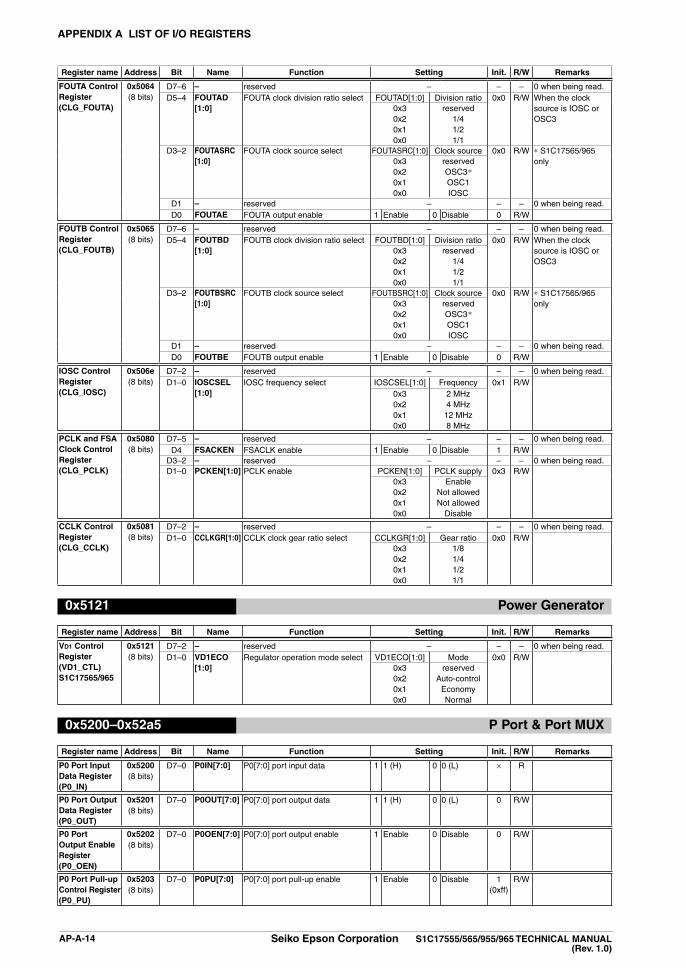
aPPenDiX a liST OF i/O ReGiSTeRS
aP-a-14 Seiko epson Corporation S1C17555/565/955/965 TeChniCal Manual (Rev. 1.0)
Register name address Bit name Function Setting init. R/W Remarks
FOuTa Control Register(ClG_FOuTa)
0x5064(8 bits)
D7–6 – reserved – – – 0 when being read.D5–4 FOuTaD
[1:0]FOUTA clock division ratio select FOUTAD[1:0] Division ratio 0x0 R/W When the clock
source is IOSC or OSC3
0x30x20x10x0
reserved1/41/21/1
D3–2 FOuTaSRC[1:0]
FOUTA clock source select FOUTASRC[1:0] Clock source 0x0 R/W * S1C17565/965 only0x3
0x20x10x0
reservedOSC3*OSC1IOSC
D1 – reserved – – – 0 when being read.D0 FOuTae FOUTA output enable 1 Enable 0 Disable 0 R/W
FOuTB Control Register(ClG_FOuTB)
0x5065(8 bits)
D7–6 – reserved – – – 0 when being read.D5–4 FOuTBD
[1:0]FOUTB clock division ratio select FOUTBD[1:0] Division ratio 0x0 R/W When the clock
source is IOSC or OSC3
0x30x20x10x0
reserved1/41/21/1
D3–2 FOuTBSRC[1:0]
FOUTB clock source select FOUTBSRC[1:0] Clock source 0x0 R/W * S1C17565/965 only0x3
0x20x10x0
reservedOSC3*OSC1IOSC
D1 – reserved – – – 0 when being read.D0 FOuTBe FOUTB output enable 1 Enable 0 Disable 0 R/W
iOSC Control Register(ClG_iOSC)
0x506e(8 bits)
D7–2 – reserved – – – 0 when being read.D1–0 iOSCSel
[1:0]IOSC frequency select IOSCSEL[1:0] Frequency 0x1 R/W
0x30x20x10x0
2 MHz4 MHz
12 MHz8 MHz
PClK and FSa Clock Control Register(ClG_PClK)
0x5080(8 bits)
D7–5 – reserved – – – 0 when being read.D4 FSaCKen FSACLK enable 1 Enable 0 Disable 1 R/W
D3–2 – reserved – – – 0 when being read.D1–0 PCKen[1:0] PCLK enable PCKEN[1:0] PCLK supply 0x3 R/W
0x30x20x10x0
EnableNot allowedNot allowed
Disable
CClK Control Register(ClG_CClK)
0x5081(8 bits)
D7–2 – reserved – – – 0 when being read.D1–0 CClKGR[1:0] CCLK clock gear ratio select CCLKGR[1:0] Gear ratio 0x0 R/W
0x30x20x10x0
1/81/41/21/1
0x5121 Power Generator
Register name address Bit name Function Setting init. R/W Remarks
VD1 Control Register(VD1_CTl)S1C17565/965
0x5121(8 bits)
D7–2 – reserved – – – 0 when being read.D1–0 VD1eCO
[1:0]Regulator operation mode select VD1ECO[1:0] Mode 0x0 R/W
0x30x20x10x0
reservedAuto-control
EconomyNormal
0x5200–0x52a5 P Port & Port MuX
Register name address Bit name Function Setting init. R/W Remarks
P0 Port input Data Register(P0_in)
0x5200(8 bits)
D7–0 P0in[7:0] P0[7:0] port input data 1 1 (H) 0 0 (L) × R
P0 Port Output Data Register(P0_OuT)
0x5201(8 bits)
D7–0 P0OuT[7:0] P0[7:0] port output data 1 1 (H) 0 0 (L) 0 R/W
P0 Port Output enable Register(P0_Oen)
0x5202(8 bits)
D7–0 P0Oen[7:0] P0[7:0] port output enable 1 Enable 0 Disable 0 R/W
P0 Port Pull-up Control Register(P0_Pu)
0x5203(8 bits)
D7–0 P0Pu[7:0] P0[7:0] port pull-up enable 1 Enable 0 Disable 1(0xff)
R/W

aPPenDiX a liST OF i/O ReGiSTeRS
S1C17555/565/955/965 TeChniCal Manual Seiko epson Corporation aP-a-15(Rev. 1.0)
Register name address Bit name Function Setting init. R/W Remarks
P0 Port interrupt Mask Register(P0_iMSK)
0x5205(8 bits)
D7–0 P0ie[7:0] P0[7:0] port interrupt enable 1 Enable 0 Disable 0 R/W
P0 Port interrupt edge Select Register(P0_eDGe)
0x5206(8 bits)
D7–0 P0eDGe[7:0] P0[7:0] port interrupt edge select 1 Falling edge 0 Rising edge 0 R/W
P0 Port interrupt Flag Register(P0_iFlG)
0x5207(8 bits)
D7–0 P0iF[7:0] P0[7:0] port interrupt flag 1 Cause of interrupt occurred
0 Cause of interrupt not occurred
0 R/W Reset by writing 1.
P0 Port Chattering Filter Control Register(P0_ChaT)
0x5208(8 bits)
D7 – reserved – – – 0 when being read.D6–4 P0CF2[2:0] P0[7:4] chattering filter time P0CF2[2:0] Filter time 0x0 R/W
0x70x60x50x40x30x20x10x0
16384/fPCLK
8192/fPCLK
4096/fPCLK
2048/fPCLK
1024/fPCLK
512/fPCLK
256/fPCLK
NoneD3 – reserved – – – 0 when being read.
D2–0 P0CF1[2:0] P0[3:0] chattering filter time P0CF1[2:0] Filter time 0x0 R/W0x70x60x50x40x30x20x10x0
16384/fPCLK
8192/fPCLK
4096/fPCLK
2048/fPCLK
1024/fPCLK
512/fPCLK
256/fPCLK
None
P0 Port Key-entry Reset Configuration Register(P0_KRST)
0x5209(8 bits)
D7–2 – reserved – – – 0 when being read.D1–0 P0KRST[1:0] P0 port key-entry reset
configurationP0KRST[1:0] Configuration 0x0 R/W
0x30x20x10x0
P0[3:0] = 0P0[2:0] = 0P0[1:0] = 0
Disable
P0 Port input enable Register(P0_ien)
0x520a(8 bits)
D7–0 P0ien[7:0] P0[7:0] port input enable 1 Enable 0 Disable 1(0xff)
R/W
P1 Port input Data Register(P1_in)
0x5210(8 bits)
D7–0 P1in[7:0] P1[7:0] port input data 1 1 (H) 0 0 (L) × R
P1 Port Output Data Register(P1_OuT)
0x5211(8 bits)
D7–0 P1OuT[7:0] P1[7:0] port output data 1 1 (H) 0 0 (L) 0 R/W
P1 Port Output enable Register(P1_Oen)
0x5212(8 bits)
D7–0 P1Oen[7:0] P1[7:0] port output enable 1 Enable 0 Disable 0 R/W
P1 Port Pull-up Control Register(P1_Pu)
0x5213(8 bits)
D7–0 P1Pu[7:0] P1[7:0] port pull-up enable 1 Enable 0 Disable 1(0xff)
R/W
P1 Port interrupt Mask Register(P1_iMSK)
0x5215(8 bits)
D7–0 P1ie[7:0] P1[7:0] port interrupt enable 1 Enable 0 Disable 0 R/W
P1 Port interrupt edge Select Register(P1_eDGe)
0x5216(8 bits)
D7–0 P1eDGe[7:0] P1[7:0] port interrupt edge select 1 Falling edge 0 Rising edge 0 R/W
P1 Port interrupt Flag Register(P1_iFlG)
0x5217(8 bits)
D7–0 P1iF[7:0] P1[7:0] port interrupt flag 1 Cause of interrupt occurred
0 Cause of interrupt not occurred
0 R/W Reset by writing 1.

aPPenDiX a liST OF i/O ReGiSTeRS
aP-a-16 Seiko epson Corporation S1C17555/565/955/965 TeChniCal Manual (Rev. 1.0)
Register name address Bit name Function Setting init. R/W Remarks
P1 Port Chattering Filter Control Register(P1_ChaT)
0x5218(8 bits)
D7 – reserved – – – 0 when being read.D6–4 P1CF2[2:0] P1[7:4] chattering filter time P1CF2[2:0] Filter time 0x0 R/W
0x70x60x50x40x30x20x10x0
16384/fPCLK
8192/fPCLK
4096/fPCLK
2048/fPCLK
1024/fPCLK
512/fPCLK
256/fPCLK
NoneD3 – reserved – – – 0 when being read.
D2–0 P1CF1[2:0] P1[3:0] chattering filter time P1CF1[2:0] Filter time 0x0 R/W0x70x60x50x40x30x20x10x0
16384/fPCLK
8192/fPCLK
4096/fPCLK
2048/fPCLK
1024/fPCLK
512/fPCLK
256/fPCLK
None
P1 Port input enable Register(P1_ien)
0x521a(8 bits)
D7–0 P1ien[7:0] P1[7:0] port input enable 1 Enable 0 Disable 1(0xff)
R/W
P2 Port input Data Register(P2_in)
0x5220(8 bits)
D7–4 P2in[7:4] P2[7:4] port input data 1 1 (H) 0 0 (L) × R S1C17565/965– reserved – – – 0 when being read.
S1C17555/955D3–0 P2in[3:0] P2[3:0] port input data 1 1 (H) 0 0 (L) × R
P2 Port Output Data Register(P2_OuT)
0x5221(8 bits)
D7–4 P2OuT[7:4] P2[7:4] port output data 1 1 (H) 0 0 (L) 0 R/W S1C17565/965– reserved – – – 0 when being read.
S1C17555/955D3–0 P2OuT[3:0] P2[3:0] port output data 1 1 (H) 0 0 (L) 0 R/W
P2 Port Output enable Register(P2_Oen)
0x5222(8 bits)
D7–4 P2Oen[7:4] P2[7:4] port output enable 1 Enable 0 Disable 0 R/W S1C17565/965– reserved – – – 0 when being read.
S1C17555/955D3–0 P2Oen[3:0] P2[3:0] port output enable 1 Enable 0 Disable 0 R/W
P2 Port Pull-up Control Register(P2_Pu)
0x5223(8 bits)
D7–4 P2Pu[7:4] P2[7:4] port pull-up enable 1 Enable 0 Disable 1(0xf)
R/W S1C17565/965
– reserved – – – 0 when being read.S1C17555/955
D3–0 P2Pu[3:0] P2[3:0] port pull-up enable 1 Enable 0 Disable 1(0xf)
R/W
P2 Port interrupt Mask Register(P2_iMSK)
0x5225(8 bits)
D7–4 P2ie[7:4] P2[7:4] port interrupt enable 1 Enable 0 Disable 0 R/W S1C17565/965– reserved – – – 0 when being read.
S1C17555/955D3–0 P2ie[3:0] P2[3:0] port interrupt enable 1 Enable 0 Disable 0 R/W
P2 Port interrupt edge Select Register(P2_eDGe)
0x5226(8 bits)
D7–4 P2eDGe[7:4] P2[7:4] port interrupt edge select 1 Falling edge 0 Rising edge 0 R/W S1C17565/965– reserved – – – 0 when being read.
S1C17555/955D3–0 P2eDGe[3:0] P2[3:0] port interrupt edge select 1 Falling edge 0 Rising edge 0 R/W
P2 Port interrupt Flag Register(P2_iFlG)
0x5227(8 bits)
D7–4 P2iF[7:4] P2[7:4] port interrupt flag 1 Cause of interrupt occurred
0 Cause of interrupt not occurred
0 R/W Reset by writing 1.S1C17565/965
– reserved – – – 0 when being read.S1C17555/955
D3–0 P2iF[3:0] P2[3:0] port interrupt flag 1 Cause of interrupt occurred
0 Cause of interrupt not occurred
0 R/W Reset by writing 1.

aPPenDiX a liST OF i/O ReGiSTeRS
S1C17555/565/955/965 TeChniCal Manual Seiko epson Corporation aP-a-17(Rev. 1.0)
Register name address Bit name Function Setting init. R/W Remarks
P2 Port Chattering Filter Control Register(P2_ChaT)
0x5228(8 bits)
D7 – reserved – – – 0 when being read.D6–4 P2CF2[2:0] P2[7:4] chattering filter time P2CF2[2:0] Filter time 0x0 R/W S1C17565/965
0x70x60x50x40x30x20x10x0
16384/fPCLK
8192/fPCLK
4096/fPCLK
2048/fPCLK
1024/fPCLK
512/fPCLK
256/fPCLK
None– reserved – – – 0 when being read.
S1C17555/955D3 – reserved – – – 0 when being read.
D2–0 P2CF1[2:0] P2[3:0] chattering filter time P2CF1[2:0] Filter time 0x0 R/W0x70x60x50x40x30x20x10x0
16384/fPCLK
8192/fPCLK
4096/fPCLK
2048/fPCLK
1024/fPCLK
512/fPCLK
256/fPCLK
None
P2 Port input enable Register(P2_ien)S1C17565/965
0x522a(8 bits)
D7–4 P2ien[7:4] P2[7:4] port input enable 1 Enable 0 Disable 1(0xf)
R/W S1C17565/965
– reserved – – – 0 when being read.S1C17555/955
D3–0 P2ien[3:0] P2[3:0] port input enable 1 Enable 0 Disable 1(0xf)
R/W
P0[3:0] Port Function Select Register(P00_03PMuX)
0x52a0(8 bits)
D7–6 P03MuX[1:0] P03 port function select P03MUX[1:0] Function 0x0 R/W0x30x20x10x0
reservedreserved#SPISS0
P03D5–4 P02MuX[1:0] P02 port function select P02MUX[1:0] Function 0x0 R/W
0x30x20x10x0
SDASSDAM
SPICLK0P02
D3–2 P01MuX[1:0] P01 port function select P01MUX[1:0] Function 0x0 R/W0x30x20x10x0
SCLSSCLMSDO0P01
D1–0 P00MuX[1:0] P00 port function select P00MUX[1:0] Function 0x0 R/W0x30x20x10x0
reservedreserved
SDI0P00
P0[7:4] Port Function Select Register(P04_07PMuX)
0x52a1(8 bits)
D7–6 P07MuX[1:0] P07 port function select P07MUX[1:0] Function 0x0 R/W0x30x20x10x0
reservedSCLSSCLMP07
D5–4 P06MuX[1:0] P06 port function select P06MUX[1:0] Function 0x0 R/W0x30x20x10x0
#BFRFOUTASCLK0
P06D3–2 P05MuX[1:0] P05 port function select P05MUX[1:0] Function 0x0 R/W
0x30x20x10x0
reservedreservedSOUT0
P05D1–0 P04MuX[1:0] P04 port function select P04MUX[1:0] Function 0x0 R/W
0x30x20x10x0
reservedreserved
SIN0P04
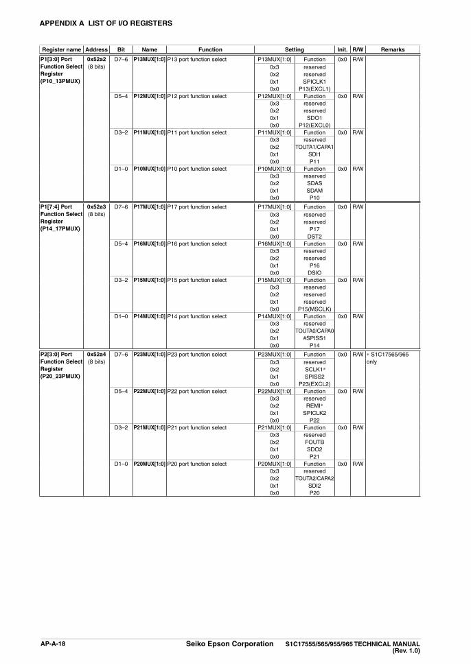
aPPenDiX a liST OF i/O ReGiSTeRS
aP-a-18 Seiko epson Corporation S1C17555/565/955/965 TeChniCal Manual (Rev. 1.0)
Register name address Bit name Function Setting init. R/W Remarks
P1[3:0] Port Function Select Register(P10_13PMuX)
0x52a2(8 bits)
D7–6 P13MuX[1:0] P13 port function select P13MUX[1:0] Function 0x0 R/W0x30x20x10x0
reservedreservedSPICLK1
P13(EXCL1)D5–4 P12MuX[1:0] P12 port function select P12MUX[1:0] Function 0x0 R/W
0x30x20x10x0
reservedreserved
SDO1P12(EXCL0)
D3–2 P11MuX[1:0] P11 port function select P11MUX[1:0] Function 0x0 R/W0x30x20x10x0
reservedTOUTA1/CAPA1
SDI1P11
D1–0 P10MuX[1:0] P10 port function select P10MUX[1:0] Function 0x0 R/W0x30x20x10x0
reservedSDASSDAMP10
P1[7:4] Port Function Select Register(P14_17PMuX)
0x52a3(8 bits)
D7–6 P17MuX[1:0] P17 port function select P17MUX[1:0] Function 0x0 R/W0x30x20x10x0
reservedreserved
P17DST2
D5–4 P16MuX[1:0] P16 port function select P16MUX[1:0] Function 0x0 R/W0x30x20x10x0
reservedreserved
P16DSIO
D3–2 P15MuX[1:0] P15 port function select P15MUX[1:0] Function 0x0 R/W0x30x20x10x0
reservedreservedreserved
P15(MSCLK)D1–0 P14MuX[1:0] P14 port function select P14MUX[1:0] Function 0x0 R/W
0x30x20x10x0
reservedTOUTA0/CAPA0
#SPISS1P14
P2[3:0] Port Function Select Register(P20_23PMuX)
0x52a4(8 bits)
D7–6 P23MuX[1:0] P23 port function select P23MUX[1:0] Function 0x0 R/W * S1C17565/965 only0x3
0x20x10x0
reserved SCLK1*SPISS2
P23(EXCL2)D5–4 P22MuX[1:0] P22 port function select P22MUX[1:0] Function 0x0 R/W
0x30x20x10x0
reservedREMI*
SPICLK2P22
D3–2 P21MuX[1:0] P21 port function select P21MUX[1:0] Function 0x0 R/W0x30x20x10x0
reservedFOUTBSDO2P21
D1–0 P20MuX[1:0] P20 port function select P20MUX[1:0] Function 0x0 R/W0x30x20x10x0
reservedTOUTA2/CAPA2
SDI2P20

aPPenDiX a liST OF i/O ReGiSTeRS
S1C17555/565/955/965 TeChniCal Manual Seiko epson Corporation aP-a-19(Rev. 1.0)
Register name address Bit name Function Setting init. R/W Remarks
P2[7:4] Port Function Select Register(P24_27PMuX)S1C17565/965
0x52a5(8 bits)
D7–6 P27MuX[1:0] P27 port function select P27MUX[1:0] Function 0x0 R/W0x30x20x10x0
reservedSDASSDAMP27
D5–4 P26MuX[1:0] P26 port function select P26MUX[1:0] Function 0x0 R/W0x30x20x10x0
reservedSCLSSCLMP26
D3–2 P25MuX[1:0] P25 port function select P25MUX[1:0] Function 0x0 R/W0x30x20x10x0
reservedREMOSOUT1
P25D1–0 P24MuX[1:0] P24 port function select P24MUX[1:0] Function 0x0 R/W
0x30x20x10x0
reservedTOUTA3/CAPA3
SIN1P24
0x4020, 0x5322–0x532c MiSC Registers
Register name address Bit name Function Setting init. R/W Remarks
Prescaler Control Register(MiSC_PSC)
0x4020(8 bits)
D7–2 – reserved – – – 0 when being read.D1 PRunD Run/stop select in debug mode 1 Run 0 Stop 0 R/WD0 – reserved – – – 0 when being read.
Debug Mode Control Register 2(MiSC_DMODe2)
0x5322(16 bits)
D15–1 – reserved – – – 0 when being read.
D0 DBRun2 Run/stop select in debug mode(except PCLK peripheral circuits)
1 Run 0 Stop 0 R/W
MiSC Protect Register(MiSC_PROT)
0x5324(16 bits)
D15–0 PROT[15:0] MISC register write protect Writing 0x96 removes the write protection of the MISC regis-ters (0x5326–0x532a).Writing another value set the write protection.
0x0 R/W
iRaM Size Register(MiSC_iRaMSZ)
0x5326(16 bits)
D15–9 – reserved – – – 0 when being read.D8 DBaDR Debug base address select 1 0x0 0 0xfffc00 0 R/WD7 – reserved – – – 0 when being read.
D6–4 iRaMaCTSZ[2:0]
IRAM actual size 0x2 (= 4KB) 0x2 R
D3 – reserved – – – 0 when being read.D2–0 iRaMSZ[2:0] IRAM size select IRAMSZ[2:0] Size 0x2 R/W
0x7–0x60x50x40x30x2
0x1–0x0
reserved512B1KB2KB4KB
reserved
Vector Table address low Register(MiSC_TTBRl)
0x5328(16 bits)
D15–8 TTBR[15:8] Vector table base address A[15:8] 0x0–0xff 0x80 R/WD7–0 TTBR[7:0] Vector table base address A[7:0]
(fixed at 0)0x0 0x0 R
Vector Table address high Register (MiSC_TTBRh)
0x532a(16 bits)
D15–8 – reserved – – – 0 when being read.D7–0 TTBR[23:16] Vector table base address
A[23:16]0x0–0xff 0x0 R/W
PSR Register(MiSC_PSR)
0x532c(16 bits)
D15–8 – reserved – – – 0 when being read.D7–5 PSRil[2:0] PSR interrupt level (IL) bits 0x0 to 0x7 0x0 R
D4 PSRie PSR interrupt enable (IE) bit 1 1 (enable) 0 0 (disable) 0 RD3 PSRC PSR carry (C) flag 1 1 (set) 0 0 (cleared) 0 RD2 PSRV PSR overflow (V) flag 1 1 (set) 0 0 (cleared) 0 RD1 PSRZ PSR zero (Z) flag 1 1 (set) 0 0 (cleared) 0 RD0 PSRn PSR negative (N) flag 1 1 (set) 0 0 (cleared) 0 R
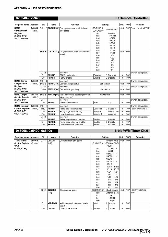
aPPenDiX a liST OF i/O ReGiSTeRS
aP-a-20 Seiko epson Corporation S1C17555/565/955/965 TeChniCal Manual (Rev. 1.0)
0x5340–0x5346 iR Remote Controller
Register name address Bit name Function Setting init. R/W Remarks
ReMC Configuration Register(ReMC_CFG)S1C17565/965
0x5340(16 bits)
D15–12 CGClK[3:0] Carrier generator clock division ratio select
CGCLK[3:0]LCCLK[3:0]
Division ratio0x0 R/W Source clock = PCLK
0xf0xe0xd0xc0xb0xa0x90x80x70x60x50x40x30x20x10x0
reserved1/163841/81921/40961/20481/10241/5121/2561/1281/641/321/161/81/41/21/1
D11–8 lCClK[3:0] Length counter clock division ratio select
0x0 R/W
D7–2 – reserved – – – 0 when being read.D1 ReMMD REMC mode select 1 Receive 0 Transmit 0 R/WD0 ReMen REMC enable 1 Enable 0 Disable 0 R/W
ReMC Carrier length Setup Register(ReMC_CaR)S1C17565/965
0x5342(16 bits)
D15–14 – reserved – – – 0 when being read.D13–8 ReMCl[5:0] Carrier L length setup 0x0 to 0x3f 0x0 R/WD7–6 – reserved – – – 0 when being read.D5–0 ReMCh[5:0] Carrier H length setup 0x0 to 0x3f 0x0 R/W
ReMC length Counter Register(ReMC_lCnT)S1C17565/965
0x5344(16 bits)
D15–8 ReMlen[7:0] Transmit/receive data length count(down counter)
0x0 to 0xff 0x0 R/W
D7–1 – reserved – – – 0 when being read.D0 ReMDT Transmit/receive data 1 1 (H) 0 0 (L) 0 R/W
ReMC interrupt Control Register(ReMC_inT)S1C17565/965
0x5346(16 bits)
D15–11 – reserved – – – 0 when being read.D10 ReMFiF Falling edge interrupt flag 1 Cause of
interrupt occurred
0 Cause of interrupt not occurred
0 R/W Reset by writing 1.D9 ReMRiF Rising edge interrupt flag 0 R/WD8 ReMuiF Underflow interrupt flag 0 R/W
D7–3 – reserved – – – 0 when being read.D2 ReMFie Falling edge interrupt enable 1 Enable 0 Disable 0 R/WD1 ReMRie Rising edge interrupt enable 1 Enable 0 Disable 0 R/WD0 ReMuie Underflow interrupt enable 1 Enable 0 Disable 0 R/W
0x5068, 0x5400–0x540c 16-bit PWM Timer Ch.0
Register name address Bit name Function Setting init. R/W Remarks
T16a2 Clock Control Register Ch.0 (T16a_ClK0)
0x5068(8 bits)
D7–4 ClKDiV[3:0]
Clock division ratio selectCLKDIV[3:0]
Division ratio 0x0 R/WOSC3 or
IOSCOSC1
0xf0xe0xd0xc0xb0xa0x90x80x70x60x50x40x30x20x10x0
1/327681/163841/81921/40961/20481/10241/5121/2561/1281/641/321/161/81/41/21/1
–––––––
1/2561/1281/641/321/161/81/41/21/1
D3–2 ClKSRC[1:0]
Clock source select CLKSRC[1:0] Clock source 0x0 R/W * S1C17565/965 only0x3
0x20x10x0
External clockOSC3*OSC1IOSC
D1 MulTiMD Multi-comparator/capture mode select
1 Multi 0 Normal 0 R/W
D0 ClKen Count clock enable 1 Enable 0 Disable 0 R/W

aPPenDiX a liST OF i/O ReGiSTeRS
S1C17555/565/955/965 TeChniCal Manual Seiko epson Corporation aP-a-21(Rev. 1.0)
Register name address Bit name Function Setting init. R/W Remarks
T16a2 Counter Ch.0 Control Register(T16a_CTl0)
0x5400(16 bits)
D15–7 – reserved – – – 0 when being read.D6 hCM Half clock mode enable 1 Enable 0 Disable 0 R/W
D5–4 CCaBCnT[1:0]
Counter select CCABCNT[1:0] Counter Ch. 0x0 R/W0x30x20x10x0
Ch.3Ch.2Ch.1Ch.0
D3 CBuFen Compare buffer enable 1 Enable 0 Disable 0 R/WD2 TRMD Count mode select 1 One-shot 0 Repeat 0 R/WD1 PReSeT Counter reset 1 Reset 0 Ignored 0 W 0 when being read.D0 PRun Counter run/stop control 1 Run 0 Stop 0 R/W
T16a2 Counter Ch.0 Data Register(T16a_TC0)
0x5402(16 bits)
D15–0 T16aTC[15:0]
Counter dataT16ATC15 = MSBT16ATC0 = LSB
0x0 to 0xffff 0x0 R
T16a2 Comparator/Capture Ch.0 Control Register(T16a_CCCTl0)
0x5404(16 bits)
D15–12 – reserved – 0x0 – Do not set to 1.D11–10 – reserved – – – 0 when being read.
D9–8 – reserved – 0 – Do not set to 1.D7–6 CaPaTRG
[1:0]Capture A trigger select CAPATRG[1:0] Trigger edge 0x0 R/W
0x30x20x10x0
↑ and ↓↓↑
NoneD5–4 TOuTaMD
[1:0]TOUTA mode select TOUTAMD[1:0] Mode 0x0 R/W
0x30x20x10x0
cmp B: ↑ or ↓cmp A: ↑ or ↓cmp A: ↑, B: ↓
OffD3–2 – reserved – – – 0 when being read.
D1 TOuTainV TOUTA invert 1 Invert 0 Normal 0 R/WD0 CCaMD T16A_CCA register mode select 1 Capture 0 Comparator 0 R/W
T16a2 Comparator/Capture Ch.0 a Data Register(T16a_CCa0)
0x5406(16 bits)
D15–0 CCa[15:0] Compare/capture A dataCCA15 = MSBCCA0 = LSB
0x0 to 0xffff 0x0 R/W
T16a2 Comparator/Capture Ch.0 B Data Register(T16a_CCB0)
0x5408(16 bits)
D15–0 CCB[15:0] Compare B dataCCB15 = MSBCCB0 = LSB
0x0 to 0xffff 0x0 R/W
T16a2 Comparator/Capture Ch.0 interrupt enable Register(T16a_ien0)
0x540a(16 bits)
D15–6 – reserved – – – 0 when being read.D5 – reserved – 0 – Do not set to 1.D4 CaPaOWie Capture A overwrite interrupt enable 1 Enable 0 Disable 0 R/WD3 – reserved – 0 – Do not set to 1.D2 CaPaie Capture A interrupt enable 1 Enable 0 Disable 0 R/WD1 CBie Compare B interrupt enable 1 Enable 0 Disable 0 R/WD0 Caie Compare A interrupt enable 1 Enable 0 Disable 0 R/W
T16a2 Comparator/Capture Ch.0 interrupt Flag Register(T16a_iFlG0)
0x540c(16 bits)
D15–5 – reserved – – – 0 when being read.D4 CaPaOWiF Capture A overwrite interrupt flag 1 Occurred 0 Not occurred 0 R/W Reset by writing 1.D3 – reserved – – – 0 when being read.D2 CaPaiF Capture A interrupt flag 1 Cause of
interrupt occurred
0 Cause of interrupt not occurred
0 R/W Reset by writing 1.D1 CBiF Compare B interrupt flag 0 R/WD0 CaiF Compare A interrupt flag 0 R/W

aPPenDiX a liST OF i/O ReGiSTeRS
aP-a-22 Seiko epson Corporation S1C17555/565/955/965 TeChniCal Manual (Rev. 1.0)
0x5069, 0x5420–0x542c 16-bit PWM Timer Ch.1
Register name address Bit name Function Setting init. R/W Remarks
T16a2 Clock Control Register Ch.1(T16a_ClK1)
0x5069(8 bits)
D7–4 ClKDiV[3:0]
Clock division ratio selectCLKDIV[3:0]
Division ratio 0x0 R/WOSC3 or
IOSCOSC1
0xf0xe0xd0xc0xb0xa0x90x80x70x60x50x40x30x20x10x0
1/327681/163841/81921/40961/20481/10241/5121/2561/1281/641/321/161/81/41/21/1
–––––––
1/2561/1281/641/321/161/81/41/21/1
D3–2 ClKSRC[1:0]
Clock source select CLKSRC[1:0] Clock source 0x0 R/W * S1C17565/965 only0x3
0x20x10x0
External clockOSC3*OSC1IOSC
D1 – reserved – – –D0 ClKen Count clock enable 1 Enable 0 Disable 0 R/W
T16a2 Counter Ch.1 Control Register(T16a_CTl1)
0x5420(16 bits)
D15–7 – reserved – – – 0 when being read.D6 hCM Half clock mode enable 1 Enable 0 Disable 0 R/W
D5–4 CCaBCnT[1:0]
Counter select CCABCNT[1:0] Counter Ch. 0x0 R/W0x30x20x10x0
Ch.3Ch.2Ch.1Ch.0
D3 CBuFen Compare buffer enable 1 Enable 0 Disable 0 R/WD2 TRMD Count mode select 1 One-shot 0 Repeat 0 R/WD1 PReSeT Counter reset 1 Reset 0 Ignored 0 W 0 when being read.D0 PRun Counter run/stop control 1 Run 0 Stop 0 R/W
T16a2 Counter Ch.1 Data Register(T16a_TC1)
0x5422(16 bits)
D15–0 T16aTC[15:0]
Counter dataT16ATC15 = MSBT16ATC0 = LSB
0x0 to 0xffff 0x0 R
T16a2 Comparator/Capture Ch.1 Control Register(T16a_CCCTl1)
0x5424(16 bits)
D15–12 – reserved – 0x0 – Do not set to 1.D11–10 – reserved – – – 0 when being read.
D9–8 – reserved – 0 – Do not set to 1.D7–6 CaPaTRG
[1:0]Capture A trigger select CAPATRG[1:0] Trigger edge 0x0 R/W
0x30x20x10x0
↑ and ↓↓↑
NoneD5–4 TOuTaMD
[1:0]TOUTA mode select TOUTAMD[1:0] Mode 0x0 R/W
0x30x20x10x0
cmp B: ↑ or ↓cmp A: ↑ or ↓cmp A: ↑, B: ↓
OffD3–2 – reserved – – – 0 when being read.
D1 TOuTainV TOUTA invert 1 Invert 0 Normal 0 R/WD0 CCaMD T16A_CCA register mode select 1 Capture 0 Comparator 0 R/W
T16a2 Comparator/Capture Ch.1 a Data Register(T16a_CCa1)
0x5426(16 bits)
D15–0 CCa[15:0] Compare/capture A dataCCA15 = MSBCCA0 = LSB
0x0 to 0xffff 0x0 R/W
T16a2 Comparator/Capture Ch.1 B Data Register(T16a_CCB1)
0x5428(16 bits)
D15–0 CCB[15:0] Compare B dataCCB15 = MSBCCB0 = LSB
0x0 to 0xffff 0x0 R/W
T16a2 Comparator/Capture Ch.1 interrupt enable Register(T16a_ien1)
0x542a(16 bits)
D15–6 – reserved – – – 0 when being read.D5 – reserved – 0 – Do not set to 1.D4 CaPaOWie Capture A overwrite interrupt enable 1 Enable 0 Disable 0 R/WD3 – reserved – 0 – Do not set to 1.D2 CaPaie Capture A interrupt enable 1 Enable 0 Disable 0 R/WD1 CBie Compare B interrupt enable 1 Enable 0 Disable 0 R/WD0 Caie Compare A interrupt enable 1 Enable 0 Disable 0 R/W

aPPenDiX a liST OF i/O ReGiSTeRS
S1C17555/565/955/965 TeChniCal Manual Seiko epson Corporation aP-a-23(Rev. 1.0)
Register name address Bit name Function Setting init. R/W Remarks
T16a2 Comparator/Capture Ch.1 interrupt Flag Register(T16a_iFlG1)
0x542c(16 bits)
D15–5 – reserved – – – 0 when being read.D4 CaPaOWiF Capture A overwrite interrupt flag 1 Occurred 0 Not occurred 0 R/W Reset by writing 1.D3 – reserved – – – 0 when being read.D2 CaPaiF Capture A interrupt flag 1 Cause of
interrupt occurred
0 Cause of interrupt not occurred
0 R/W Reset by writing 1.D1 CBiF Compare B interrupt flag 0 R/WD0 CaiF Compare A interrupt flag 0 R/W
0x506a, 0x5440–0x544c 16-bit PWM Timer Ch.2
Register name address Bit name Function Setting init. R/W Remarks
T16a2 Clock Control Register Ch.2(T16a_ClK2)
0x506a(8 bits)
D7–4 ClKDiV[3:0]
Clock division ratio selectCLKDIV[3:0]
Division ratio 0x0 R/WOSC3 or
IOSCOSC1
0xf0xe0xd0xc0xb0xa0x90x80x70x60x50x40x30x20x10x0
1/327681/163841/81921/40961/20481/10241/5121/2561/1281/641/321/161/81/41/21/1
–––––––
1/2561/1281/641/321/161/81/41/21/1
D3–2 ClKSRC[1:0]
Clock source select CLKSRC[1:0] Clock source 0x0 R/W * S1C17565/965 only0x3
0x20x10x0
External clockOSC3*OSC1IOSC
D1 – reserved – – –D0 ClKen Count clock enable 1 Enable 0 Disable 0 R/W
T16a2 Counter Ch.2 Control Register(T16a_CTl2)
0x5440(16 bits)
D15–7 – reserved – – – 0 when being read.D6 hCM Half clock mode enable 1 Enable 0 Disable 0 R/W
D5–4 CCaBCnT[1:0]
Counter select CCABCNT[1:0] Counter Ch. 0x0 R/W0x30x20x10x0
Ch.3Ch.2Ch.1Ch.0
D3 CBuFen Compare buffer enable 1 Enable 0 Disable 0 R/WD2 TRMD Count mode select 1 One-shot 0 Repeat 0 R/WD1 PReSeT Counter reset 1 Reset 0 Ignored 0 W 0 when being read.D0 PRun Counter run/stop control 1 Run 0 Stop 0 R/W
T16a2 Counter Ch.2 Data Register(T16a_TC2)
0x5442(16 bits)
D15–0 T16aTC[15:0]
Counter dataT16ATC15 = MSBT16ATC0 = LSB
0x0 to 0xffff 0x0 R
T16a2 Comparator/Capture Ch.2 Control Register(T16a_CCCTl2)
0x5444(16 bits)
D15–12 – reserved – 0x0 – Do not set to 1.D11–10 – reserved – – – 0 when being read.
D9–8 – reserved – 0 – Do not set to 1.D7–6 CaPaTRG
[1:0]Capture A trigger select CAPATRG[1:0] Trigger edge 0x0 R/W
0x30x20x10x0
↑ and ↓↓↑
NoneD5–4 TOuTaMD
[1:0]TOUTA mode select TOUTAMD[1:0] Mode 0x0 R/W
0x30x20x10x0
cmp B: ↑ or ↓cmp A: ↑ or ↓cmp A: ↑, B: ↓
OffD3–2 – reserved – – – 0 when being read.
D1 TOuTainV TOUTA invert 1 Invert 0 Normal 0 R/WD0 CCaMD T16A_CCA register mode select 1 Capture 0 Comparator 0 R/W
T16a2 Comparator/Capture Ch.2 a Data Register(T16a_CCa2)
0x5446(16 bits)
D15–0 CCa[15:0] Compare/capture A dataCCA15 = MSBCCA0 = LSB
0x0 to 0xffff 0x0 R/W
T16a2 Comparator/Capture Ch.2 B Data Register(T16a_CCB2)
0x5448(16 bits)
D15–0 CCB[15:0] Compare B dataCCB15 = MSBCCB0 = LSB
0x0 to 0xffff 0x0 R/W

aPPenDiX a liST OF i/O ReGiSTeRS
aP-a-24 Seiko epson Corporation S1C17555/565/955/965 TeChniCal Manual (Rev. 1.0)
Register name address Bit name Function Setting init. R/W Remarks
T16a2 Comparator/Capture Ch.2 interrupt enable Register(T16a_ien2)
0x544a(16 bits)
D15–6 – reserved – – – 0 when being read.D5 – reserved – 0 – Do not set to 1.D4 CaPaOWie Capture A overwrite interrupt enable 1 Enable 0 Disable 0 R/WD3 – reserved – 0 – Do not set to 1.D2 CaPaie Capture A interrupt enable 1 Enable 0 Disable 0 R/WD1 CBie Compare B interrupt enable 1 Enable 0 Disable 0 R/WD0 Caie Compare A interrupt enable 1 Enable 0 Disable 0 R/W
T16a2 Comparator/Capture Ch.2 interrupt Flag Register(T16a_iFlG2)
0x544c(16 bits)
D15–5 – reserved – – – 0 when being read.D4 CaPaOWiF Capture A overwrite interrupt flag 1 Occurred 0 Not occurred 0 R/W Reset by writing 1.D3 – reserved – – – 0 when being read.D2 CaPaiF Capture A interrupt flag 1 Cause of
interrupt occurred
0 Cause of interrupt not occurred
0 R/W Reset by writing 1.D1 CBiF Compare B interrupt flag 0 R/WD0 CaiF Compare A interrupt flag 0 R/W
0x506b, 0x5460–0x546c 16-bit PWM Timer Ch.3
Register name address Bit name Function Setting init. R/W Remarks
T16a2 Clock Control Register Ch.3(T16a_ClK3)
0x506b(8 bits)
D7–4 ClKDiV[3:0]
Clock division ratio selectCLKDIV[3:0]
Division ratio 0x0 R/WOSC3 or
IOSCOSC1
0xf0xe0xd0xc0xb0xa0x90x80x70x60x50x40x30x20x10x0
1/327681/163841/81921/40961/20481/10241/5121/2561/1281/641/321/161/81/41/21/1
–––––––
1/2561/1281/641/321/161/81/41/21/1
D3–2 ClKSRC[1:0]
Clock source select CLKSRC[1:0] Clock source 0x0 R/W * S1C17565/965 only0x3
0x20x10x0
External clockOSC3*OSC1IOSC
D1 – reserved – – –D0 ClKen Count clock enable 1 Enable 0 Disable 0 R/W
T16a2 Counter Ch.3 Control Register(T16a_CTl3)
0x5460(16 bits)
D15–7 – reserved – – – 0 when being read.D6 hCM Half clock mode enable 1 Enable 0 Disable 0 R/W
D5–4 CCaBCnT[1:0]
Counter select CCABCNT[1:0] Counter Ch. 0x0 R/W0x30x20x10x0
Ch.3Ch.2Ch.1Ch.0
D3 CBuFen Compare buffer enable 1 Enable 0 Disable 0 R/WD2 TRMD Count mode select 1 One-shot 0 Repeat 0 R/WD1 PReSeT Counter reset 1 Reset 0 Ignored 0 W 0 when being read.D0 PRun Counter run/stop control 1 Run 0 Stop 0 R/W
T16a2 Counter Ch.3 Data Register(T16a_TC3)
0x5462(16 bits)
D15–0 T16aTC[15:0]
Counter dataT16ATC15 = MSBT16ATC0 = LSB
0x0 to 0xffff 0x0 R
T16a2 Comparator/Capture Ch.3 Control Register(T16a_CCCTl3)
0x5464(16 bits)
D15–12 – reserved – 0x0 – Do not set to 1.D11–10 – reserved – – – 0 when being read.
D9–8 – reserved – 0 – Do not set to 1.D7–6 CaPaTRG
[1:0]Capture A trigger select CAPATRG[1:0] Trigger edge 0x0 R/W
0x30x20x10x0
↑ and ↓↓↑
NoneD5–4 TOuTaMD
[1:0]TOUTA mode select TOUTAMD[1:0] Mode 0x0 R/W
0x30x20x10x0
cmp B: ↑ or ↓cmp A: ↑ or ↓cmp A: ↑, B: ↓
OffD3–2 – reserved – – – 0 when being read.
D1 TOuTainV TOUTA invert 1 Invert 0 Normal 0 R/WD0 CCaMD T16A_CCA register mode select 1 Capture 0 Comparator 0 R/W

aPPenDiX a liST OF i/O ReGiSTeRS
S1C17555/565/955/965 TeChniCal Manual Seiko epson Corporation aP-a-25(Rev. 1.0)
Register name address Bit name Function Setting init. R/W Remarks
T16a2 Comparator/Capture Ch.3 a Data Register(T16a_CCa3)
0x5466(16 bits)
D15–0 CCa[15:0] Compare/capture A dataCCA15 = MSBCCA0 = LSB
0x0 to 0xffff 0x0 R/W
T16a2 Comparator/Capture Ch.3 B Data Register(T16a_CCB3)
0x5468(16 bits)
D15–0 CCB[15:0] Compare B dataCCB15 = MSBCCB0 = LSB
0x0 to 0xffff 0x0 R/W
T16a2 Comparator/Capture Ch.3 interrupt enable Register(T16a_ien3)
0x546a(16 bits)
D15–6 – reserved – – – 0 when being read.D5 – reserved – 0 – Do not set to 1.D4 CaPaOWie Capture A overwrite interrupt enable 1 Enable 0 Disable 0 R/WD3 – reserved – 0 – Do not set to 1.D2 CaPaie Capture A interrupt enable 1 Enable 0 Disable 0 R/WD1 CBie Compare B interrupt enable 1 Enable 0 Disable 0 R/WD0 Caie Compare A interrupt enable 1 Enable 0 Disable 0 R/W
T16a2 Comparator/Capture Ch.3 interrupt Flag Register(T16a_iFlG3)
0x546c(16 bits)
D15–5 – reserved – – – 0 when being read.D4 CaPaOWiF Capture A overwrite interrupt flag 1 Occurred 0 Not occurred 0 R/W Reset by writing 1.D3 – reserved – – – 0 when being read.D2 CaPaiF Capture A interrupt flag 1 Cause of
interrupt occurred
0 Cause of interrupt not occurred
0 R/W Reset by writing 1.D1 CBiF Compare B interrupt flag 0 R/WD0 CaiF Compare A interrupt flag 0 R/W
0x54b0 Flash Controller
Register name address Bit name Function Setting init. R/W Remarks
FlaShC Read Wait Control Register(FlaShC_WaiT)
0x54b0(16 bits)
D15–2 – reserved – – – 0 when being read.D1–0 RDWaiT
[1:0]Flash read wait cycle RDWAIT[1:0] Wait 0x3 R/W
0x30x20x10x0
2 wait1 wait
No waitreserved
0x5071, 0x5500–0x551c 12-bit a/D Converter
Register name address Bit name Function Setting init. R/W Remarks
aDC12Sa2 Clock Control Register(aDC12_ClK)S1C17565/965
0x5071(8 bits)
D7 – reserved – – – 0 when being read.D6–4 ClKDiV
[2:0]Clock division ratio select CLKDIV[2:0] Division ratio 0x0 R/W
0x7–0x50x40x30x20x10x0
reserved1/61/81/41/21/1
D3–2 ClKSRC[1:0]
Clock source select CLKSRC[1:0] Clock source 0x0 R/W0x30x20x10x0
MSCLK (ext)OSC3
reservedIOSC
D1 – reserved – – – 0 when being read.D0 ClKen Clock enable 1 Enable 0 Disable 0 R/W
aDC12Sa2 Control Register(aDC12_CTl0)S1C17565/965
0x5500(16 bits)
D15–7 – reserved – – – 0 when being read.D6 STMD Measurement result storing mode 1 AIND[15:4] 0 AIND[11:0] 0 R/WD5 aFeTS Measurement trigger select 1 T16A2 Ch.3 0 Software 0 R/WD4 aFeMS Measurement mode select 1 Continuous 0 Single 0 R/WD3 – reserved – – – 0 when being read.D2 SOFTST Software trigger 1 Start 0 – 0 R/WD1 CTlSTP Measurement termination 1 Stop 0 – 0 R/WD0 CTlen Measurement trigger enable 1 Enable 0 Disable 0 R/W
aDC12Sa2 Measurement Channel Register(aDC12_CTl1)S1C17565/965
0x5502(16 bits)
D15–13 – reserved – – – 0 when being read.D12 MS_a8 AIN8 measurement enable 1 Enable 0 Disable 0 R/WD11 MS_a7 AIN7 measurement enable 1 Enable 0 Disable 0 R/WD10 MS_a6 AIN6 measurement enable 1 Enable 0 Disable 0 R/WD9 MS_a35 AIN3–5 measurement enable 1 Enable 0 Disable 0 R/W
D8–6 – reserved – – – 0 when being read.D5 MSBuSY Measurement busy status flag 1 Busy 0 Idle 0 RD4 MST_a8 AIN8 measurement status flag 1 Running 0 Standby 0 RD3 MST_a7 AIN7 measurement status flag 1 Running 0 Standby 0 RD2 MST_a6 AIN6 measurement status flag 1 Running 0 Standby 0 RD1 MST_a35 AIN3–5 measurement status flag 1 Running 0 Standby 0 RD0 – reserved – – – 0 when being read.

aPPenDiX a liST OF i/O ReGiSTeRS
aP-a-26 Seiko epson Corporation S1C17555/565/955/965 TeChniCal Manual (Rev. 1.0)
Register name address Bit name Function Setting init. R/W Remarks
aDC12Sa2 interrupt Control Register(aDC12_inT)S1C17565/965
0x5504(16 bits)
D15–14 – reserved – – – 0 when being read.D13 iF_all All channels completion int. flag 1 Cause of
interrupt occurred
0 Cause of interrupt not occurred
0 R/W Reset by writing 1.D12 iF_a8 AIN8 completion interrupt flag 0 R/WD11 iF_a7 AIN7 completion interrupt flag 0 R/WD10 iF_a6 AIN6 completion interrupt flag 0 R/WD9 iF_a35 AIN3–5 completion interrupt flag 0 R/W
D8–6 – reserved – – – 0 when being read.D5 ien_all All channels completion int. enable 1 Enable 0 Disable 0 R/WD4 ien_a8 AIN8 completion interrupt enable 1 Enable 0 Disable 0 R/WD3 ien_a7 AIN7 completion interrupt enable 1 Enable 0 Disable 0 R/WD2 ien_a6 AIN6 completion interrupt enable 1 Enable 0 Disable 0 R/WD1 ien_a35 AIN3–5 completion int. enable 1 Enable 0 Disable 0 R/WD0 – reserved – – – 0 when being read.
aDC12Sa2 Power Control Register(aDC12_aCTl)S1C17565/965
0x550a(16 bits)
D15–4 – reserved – – – 0 when being read.
D3 RG_Be Reference voltage source enable 1 Enable 0 Disable 0 R/WD2 RG_Ce AVDD enable 1 Enable 0 Disable 0 R/W
D1–0 – reserved – – – 0 when being read.
aDC12Sa2 ain3 Measurement Result Register(aDC12_ain3D)S1C17565/965
0x5512(16 bits)
D15–0 ainD[15:0] Measurement dataAIND[11:0] are effective when STMD = 0 (AIND[15:12] = 0)AIND[15:4] are effective when STMD = 1 (AIND[3:0] = 0)
0x0 to 0xfff 0x0 R
aDC12Sa2 ain4 Measurement Result Register(aDC12_ain4D)S1C17565/965
0x5514(16 bits)
D15–0 ainD[15:0] Measurement dataAIND[11:0] are effective when STMD = 0 (AIND[15:12] = 0)AIND[15:4] are effective when STMD = 1 (AIND[3:0] = 0)
0x0 to 0xfff 0x0 R
aDC12Sa2 ain5 Measurement Result Register(aDC12_ain5D)S1C17565/965
0x5516(16 bits)
D15–0 ainD[15:0] Measurement dataAIND[11:0] are effective when STMD = 0 (AIND[15:12] = 0)AIND[15:4] are effective when STMD = 1 (AIND[3:0] = 0)
0x0 to 0xfff 0x0 R
aDC12Sa2 ain6 Measurement Result Register(aDC12_ain6D)S1C17565/965
0x5518(16 bits)
D15–0 ainD[15:0] Measurement dataAIND[11:0] are effective when STMD = 0 (AIND[15:12] = 0)AIND[15:4] are effective when STMD = 1 (AIND[3:0] = 0)
0x0 to 0xfff 0x0 R
aDC12Sa2 ain7 Measurement Result Register(aDC12_ain7D)S1C17565/965
0x551a(16 bits)
D15–0 ainD[15:0] Measurement dataAIND[11:0] are effective when STMD = 0 (AIND[15:12] = 0)AIND[15:4] are effective when STMD = 1 (AIND[3:0] = 0)
0x0 to 0xfff 0x0 R
aDC12Sa2 ain8 Measurement Result Register(aDC12_ain8D)S1C17565/965
0x551c(16 bits)
D15–0 ainD[15:0] Measurement dataAIND[11:0] are effective when STMD = 0 (AIND[15:12] = 0)AIND[15:4] are effective when STMD = 1 (AIND[3:0] = 0)
0x0 to 0xfff 0x0 R
0x6040–0x605c 16-bit SPi
Register name address Bit name Function Setting init. R/W Remarks
SPi16 Receive Data Register(SPi16_RXD)
0x6040(16 bits)
D15–0 SPiRXD[15:0]
SPI16 receive dataSPIRXD0 = LSB
0x0 to 0xffff 0x0 R
SPi16 Transmit Data Register(SPi16_TXD)
0x6044(16 bits)
D15–0 SPiTXD[15:0]
SPI16 transmit dataSPITXD0 = LSB
0x0 to 0xffff 0x0 R/W
SPi16 Control Register 1(SPi16_CTl1)
0x6048(16 bits)
D15 – reserved – – – 0 when being read.D14–10 BPT[4:0] Data bit length setting BPT[4:0] Data bit length 0x0 R/W
0xf:
0x10x0
16 bits:
2 bits1 bit
D9 CPha Clock phase select 1 Phase 1 0 Phase 0 0 R/WD8 CPOl Clock polarity select 1 Active low 0 Active high 0 R/WD7 – reserved – – – 0 when being read.D6 MCBR[2:0] Master clock bit rate setting fSPICLK2 = fPCLK/(4×2(MCBR[2:0])) 0x0 R/W Master mode only
D3–2 – reserved – – – 0 when being read.D1 MODe Master/slave mode select 1 Master 0 Slave 0 R/WD0 ena SPI16 enable 1 Enable 0 Disable 0 R/W

aPPenDiX a liST OF i/O ReGiSTeRS
S1C17555/565/955/965 TeChniCal Manual Seiko epson Corporation aP-a-27(Rev. 1.0)
Register name address Bit name Function Setting init. R/W Remarks
SPi16 Control Register 2(SPi16_CTl2)
0x604c(16 bits)
D15–11 – reserved – – – 0 when being read.D10 SS Slave select control 1 Select 0 Deselect 0 R/W Slave mode onlyD9 SSP Slave select signal polarity select 1 Active high 0 Active low 0 R/WD8 SSC Slave select pin enable 1 Enable 0 Disable 0 R/W
D7–0 – reserved – – – 0 when being read.
SPi16 Wait Register(SPi16_WaiT)
0x6050(16 bits)
D15–11 SPiW[15:0] SPI wait cycle control 0 to 65535(SPI clock cycle)
0x0 R/W Master mode only
SPi16 Status Register(SPi16_STaT)
0x6054(16 bits)
D15–7 – reserved – – – 0 when being read.D6 BSYF Transfer busy flag 1 Busy 0 Idle 0 R Master mode onlyD5 – reserved – – – 0 when being read.D4 TDeF Transmit buffer empty flag 1 Empty 0 Not empty 1 RD3 RDOF Receive buffer overwrite error flag 1 Error 0 Normal 0 RD2 RDFF Receive buffer full flag 1 Full 0 Not full 0 R
D1–0 – reserved – – – 0 when being read.
SPi16 interrupt Control Register(SPi16_inT)
0x6058(16 bits)
D15–5 – reserved – – – 0 when being read.D4 Teie Transmit buffer empty int. enable 1 Enable 0 Disable 0 R/WD3 ROie Receive buffer overwrite error int.
enable1 Enable 0 Disable 0 R/W
D2 RFie Receive buffer full int. enable 1 Enable 0 Disable 0 R/WD1 MiRQ Software interrupt request control 1 Issue 0 Clear 0 R/WD0 iRQe SPI16 interrupt request enable 1 Enable 0 Disable 0 R/W
SPi16 Receive Data Mask Register(SPi16_MaSK)
0x605c(16 bits)
D15 – reserved – – – 0 when being read.D14–10 RXMaSK
[4:0]Receive data bit mask setting RXMASK[4:0] Valid bits 0x0 R/W
0xf0xe
:0x10x0
D[15:0]D[14:0]
:D[1:0]
D0D9–2 – reserved – – – 0 when being read.
D1 RXMe Receive data mask enable 1 Enable 0 Disable 0 R/WD0 – reserved – – – 0 when being read.
0xffff84–0xffffd0 S1C17 Core i/O
Register name address Bit name Function Setting init. R/W Remarks
Processor iD Register(iDiR)
0xffff84(8 bits)
D7–0 iDiR[7:0] Processor ID0x10: S1C17 Core
0x10 0x10 R
Debug RaM Base Register(DBRaM)
0xffff90(32 bits)
D31–24 – Unused (fixed at 0) 0x0 0x0 RD23–0 DBRaM[23:0] Debug RAM base address 0xfc0 0xf
c0R
Debug ControlRegister(DCR)
0xffffa0(8 bits)
D7 iBe4 Instruction break #4 enable 1 Enable 0 Disable 0 R/WD6 iBe3 Instruction break #3 enable 1 Enable 0 Disable 0 R/WD5 iBe2 Instruction break #2 enable 1 Enable 0 Disable 0 R/WD4 DR Debug request flag 1 Occurred 0 Not occurred 0 R/W Reset by writing 1.D3 iBe1 Instruction break #1 enable 1 Enable 0 Disable 0 R/WD2 iBe0 Instruction break #0 enable 1 Enable 0 Disable 0 R/WD1 Se Single step enable 1 Enable 0 Disable 0 R/WD0 DM Debug mode 1 Debug mode 0 User mode 0 R
instructionBreak addressRegister 1(iBaR1)
0xffffb4(32 bits)
D31–24 – reserved – – – 0 when being read.D23–0 iBaR1[23:0] Instruction break address #1
IBAR123 = MSBIBAR10 = LSB
0x0 to 0xffffff 0x0 R/W
instructionBreak addressRegister 2(iBaR2)
0xffffb8(32 bits)
D31–24 – reserved – – – 0 when being read.D23–0 iBaR2[23:0] Instruction break address #2
IBAR223 = MSBIBAR20 = LSB
0x0 to 0xffffff 0x0 R/W
instructionBreak addressRegister 3(iBaR3)
0xffffbc(32 bits)
D31–24 – reserved – – – 0 when being read.D23–0 iBaR3[23:0] Instruction break address #3
IBAR323 = MSBIBAR30 = LSB
0x0 to 0xffffff 0x0 R/W
instructionBreak addressRegister 4(iBaR4)
0xffffd0(32 bits)
D31–24 – reserved – – – 0 when being read.D23–0 iBaR4[23:0] Instruction break address #4
IBAR423 = MSBIBAR40 = LSB
0x0 to 0xffffff 0x0 R/W

aPPenDiX B POWeR SaVinG
S1C17555/565/955/965 TeChniCal Manual Seiko epson Corporation aP-B-1(Rev. 1.0)
Appendix B Power SavingCurrent consumption will vary dramatically, depending on CPU operating mode, operation clock frequency, and the peripheral circuits being operated. Listed below are the control methods for saving power.
Clock Control Power SavingB.1 This section describes clock systems that can be controlled via software and power-saving control details. For more information on control registers and control methods, refer to the respective module sections.
System SleeP (all clocks stopped)• Execute the slp instruction Execute the slp instruction when the entire system can be stopped. The CPU enters SLEEP mode and the
system clocks stop. This also stops all peripheral circuits using clocks. Starting up the CPU from SLEEP mode is therefore limited to startup using a port (described later).
System clocks• Select a low-speed clock source (CLG module) Select a low-speed oscillator for the system clock source. You can reduce current consumption by selecting
the OSC1 clock when low-speed processing is possible.
• Disable unnecessary oscillator circuits (CLG module) Operate the oscillator comprising the system clock source. Where possible, stop the other oscillators. You can
reduce current consumption by using OSC1 as the system clock and disable the IOSC and OSC3 oscillators.
CPu clock (CClK)• Execute the halt instruction Execute the halt instruction when program execution by the CPU is not required—for example, when only
the display is required or for interrupt standby. The CPU enters HALT mode and suspends operations, but the peripheral circuits maintain the status in place at the time of the halt instruction, enabling use of peripheral circuits for timers and interrupts. You can reduce power consumption even further by suspending unneces-sary oscillator and peripheral circuits before executing the halt instruction. The CPU is started from HALT mode by an interrupt from a port or the peripheral circuit operating in HALT mode.
• Select a low-speed clock gear (CLG module) The CLG module can reduce CPU clock speeds to between 1/1 and 1/8 of the system clock via the clock gear
settings. You can reduce current consumption by operating the CPU at the minimum speed required for the application.
Peripheral clock (PClK)• Stop PCLK (CLG module) Stop the PCLK clock supplied from the CLG to peripheral circuits if none of the following peripheral circuits
is required.
Peripheral circuits that use PCLK • UART Ch.0 and Ch.1 • Fine mode 16-bit timer Ch.0 and Ch.1 • 16-bit timer Ch.0 to Ch.2 • 8-bit SPI Ch.0 and Ch.1 • 16-bit SPI • I2C master • I2C slave • Power generator • P ports and port MUX (control registers, chattering filters) • MISC registers • IR remote controller

aPPenDiX B POWeR SaVinG
aP-B-2 Seiko epson Corporation S1C17555/565/955/965 TeChniCal Manual (Rev. 1.0)
PCLK is not required for the peripheral modules/functions shown below.
Peripheral circuits/functions that do not use PCLK • Clock timer • Stopwatch timer • Watchdog timer • 16-bit PWM timer Ch.0 to Ch.3 • 12-bit A/D converter • FOUTA/FOUTB outputs
Table B.1.1 shows a list of methods for clock control and starting/stopping the CPU.
1.1 Clock Control ListTable B.
Currentconsumption
OSC1 iOSC/OSC3 CPu (CClK)PClK
peripheralOSC1
peripheralCPu stopmethod
CPu startupmethod
↑Low
Stop Stop Stop Stop StopExecute slpinstruction
1
Oscillation(system CLK)
Stop Stop Stop RunExecute halt
instruction1, 2
Oscillation(system CLK)
Stop Stop Run RunExecute halt
instruction1, 2, 3
Oscillation(system CLK)
StopRun(1/1)
Run Run
OscillationOscillation
(system CLK)Stop Run Run
Execute haltinstruction
1, 2, 3
OscillationOscillation
(system CLK)Run
(low gear)Run Run
High↓ Oscillation
Oscillation(system CLK)
Run(1/1)
Run Run
HALT and SLEEP mode cancelation methods (CPU startup method)
1. Startup by port Started up by an I/O port interrupt or a debug interrupt (ICD forced break).
2. Startup by OSC1 peripheral circuit Started up by a clock timer, stopwatch timer, or watchdog timer interrupt.
3. Startup by PCLK peripheral circuit Started up by a PCLK peripheral circuit interrupt.
Reducing Power Consumption via Power Supply ControlB.2 The available power supply controls are listed below.
Regulator operating mode [S1C17565/965] When the embedded regulator is used in the S1C17565/965, it should be placed into economy mode (power
saving mode) to reduce current consumption during low-speed (32 kHz) operation or standby mode (HALT or SLEEP). For controlling economy mode, see the “Power Supply” chapter.

aPPenDiX C MOunTinG PReCauTiOnS
S1C17555/565/955/965 TeChniCal Manual Seiko epson Corporation aP-C-1(Rev. 1.0)
Appendix C Mounting PrecautionsThis section describes various precautions for circuit board design and IC mounting.
Oscillator circuit• Oscillation characteristics depend on factors such as components used (resonator, Rf, CG, CD) and circuit
board patterns. In particular, with ceramic or crystal resonators, select the appropriate external resistor (Rf) and capacitors (CG, CD) only after fully evaluating components actually mounted on the circuit board.
• Oscillator clock disturbances caused by noise may cause malfunctions. To prevent such disturbances, consid-er the following points. The latest devices, in particular, are manufactured by microscopic processes, making them especially susceptible to noise.
Areas in which noise countermeasures are especially important include the OSC2 pin and related circuit components and wiring. OSC1 pin handling is equally important. The noise precautions required for the OSC1 and OSC2 pins are described below. We also recommend applying similar noise countermeasures to the high-speed oscillator circuit, such as the OSC3 and OSC4 pins and wiring.
(1) Components such as a resonator, resistors, and capacitors connected to the OSC1 (OSC3) and OSC2 (OSC4) pins should have the shortest connections possible.
(2) Wherever possible, avoid locating digital signal lines within 3 mm of the OSC1 (OSC3) and OSC2 (OSC4) pins or related circuit components and wiring. Rapidly-switching signals, in particular, should be kept at a distance from these components. Since the spacing between layers of multi-layer printed circuit boards is a mere 0.1 mm to 0.2 mm, the above precautions also apply when positioning digital signal lines on other layers.
Never place digital signal lines alongside such components or wiring, even if more than 3 mm distance or located on other layers. Avoid crossing wires.
(3) Use VSS to shield OSC1 (OSC3) and OSC2 (OSC4) pins and related wiring (including wiring for adjacent circuit board layers). Layers wired should be adequately shielded as shown to the right. Fully ground adjacent lay-ers, where possible. At minimum, shield the area at least 5 mm around the above pins and wiring.
Even after implementing these precautions, avoid configuring digital signal lines in parallel, as described in (2) above. Avoid crossing even on discrete layers, except for lines carrying signals with low switching frequencies.
(4) After implementing these precautions, check the output clock waveform by running the actual application program within the product. Use an oscilloscope to check the FOUTA or FOUTB pin output.
You can check the quality of the OSC3 output waveform via the FOUTA/B output. Confirm that the fre-quency is as designed, is free of noise, and has minimal jitter.
You can check the quality of the OSC1 waveform via the FOUTA/B output. In particular, enlarge the areas before and after the clock rising and falling edges and take special care to confirm that the regions approxi-mately 100 ns to either side are free of clock or spiking noise.
Failure to observe precautions (1) to (3) adequately may lead to jitter in the OSC3 output and noise in the OSC1 output. Jitter in the OSC3 output will reduce operating frequencies, while noise in the OSC1 output will destabilize timers operated by the OSC1 clock as well as CPU Core operations when the system clock switches to OSC1.
Reset circuit• The reset signal input to the #RESET pin when power is turned on will vary, depending on various factors,
such as power supply start-up time, components used, and circuit board patterns. Constants such as capaci-tance and resistance should be determined through testing with real-world products.
• Components such as capacitors and resistors connected to the #RESET pin should have the shortest connec-tions possible to prevent noise-induced resets.
OSC4
OSC3
VSS
Sample VSS pattern (OSC3)
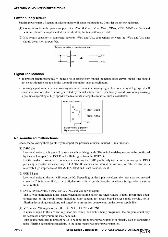
aPPenDiX C MOunTinG PReCauTiOnS
aP-C-2 Seiko epson Corporation S1C17555/565/955/965 TeChniCal Manual (Rev. 1.0)
Power supply circuit Sudden power supply fluctuations due to noise will cause malfunctions. Consider the following issues.
(1) Connections from the power supply to the *VDD (LVDD, HVDD, AVDD, VINA, VINL, VINP, and VPP) and VSS pins should be implemented via the shortest, thickest patterns possible.
(2) If a bypass capacitor is connected between *VDD and VSS, connections between the *VDD and VSS pins should be as short as possible.
*VDD
VSS
Bypass capacitor connection example
*VDD
VSS
Signal line location• To prevent electromagnetically-induced noise arising from mutual induction, large-current signal lines should
not be positioned close to circuits susceptible to noise, such as oscillators.
• Locating signal lines in parallel over significant distances or crossing signal lines operating at high speed will cause malfunctions due to noise generated by mutual interference. Specifically, avoid positioning crossing signal lines operating at high speed close to circuits susceptible to noise, such as oscillators.
OSC1, OSC3
OSC2, OSC4
VSS
Large current signal lineHigh-speed signal line
Prohibited pattern
noise-induced malfunctions Check the following three points if you suspect the presence of noise-induced IC malfunctions.
(1) DSIO pin Low-level noise to this pin will cause a switch to debug mode. The switch to debug mode can be confirmed
by the clock output from DCLK and a High signal from the DST2 pin. For the product version, we recommend connecting the DSIO pin directly to HVDD or pulling up the DISO
pin using a resistor not exceeding 10 kW. The IC includes an internal pull-up resistor. The resistor has a relatively high impedance of 100 kW to 500 kW and is not noise-resistant.
(2) #RESET pin Low-level noise to this pin will reset the IC. Depending on the input waveform, the reset may not proceed
correctly. This is more likely to occur if, due to circuit design choices, the impedance is high when the reset input is High.
(3) LVDD, HVDD, AVDD, VINA, VINL, VINP, and VSS power supply The IC will malfunction at the instant when noise falling below the rated voltage is input. Incorporate coun-
termeasures on the circuit board, including close patterns for circuit board power supply circuits, noise-filtering decoupling capacitors, and surge/noise prevention components on the power supply line.
(4) VPP pin and VPP regulator pins (C1P, C1N, C1H, C2P, and C2N) If noise is input to the VPP and regulator pins while the Flash is being programed, the program count may
be decreased or programming may be failed. Take countermeasures to prevent noise to be input from other power supplies or signals, such as connecting
noise-filtering decoupling capacitors, in the same manner as other power supplies.

aPPenDiX C MOunTinG PReCauTiOnS
S1C17555/565/955/965 TeChniCal Manual Seiko epson Corporation aP-C-3(Rev. 1.0)
Perform the inspections described above using an oscilloscope capable of observing waveforms of at least 200 MHz. It may not be possible to observe high-speed noise events with a low-speed oscilloscope.
If you detect potential noise-induced malfunctions while observing the waveform with an oscilloscope, recheck with a low-impedance (less than 1 kW) resistor connecting the relevant pin to GND or to the power supply. Malfunctions at that pin are likely if changes are visible, such as the malfunction disappearing, becoming less frequent, or the phenomena changing.
The DSIO and #RESET input circuits described above detect input signal edges and are susceptible to malfunc-tions induced by spike noise. This makes these digital signal pins the most susceptible to noise.
To reduce potential noise, keep the following two points in mind when designing circuit boards:
(A) It is important to lower the signal-driving impedance, as described above. Connect pins to the power supply or GND, with impedance of 1 kW or less, preferably 0 W. The signal lines connected should be no longer than approximately 5 mm.
(B) Parallel routing of signal lines with other digital lines on the board is undesirable, since the noise generated when the signal changes from High to Low or vice versa may adversely affect the digital lines. The sig-nal may be subject to the most noise when signal lines are laid between multiple signal lines whose states change simultaneously. Take corrective measures by shortening the parallel distance (to several cm) or separating signal lines (2 mm or more).
handling of light (for bare chip/WCSP mounting) The characteristics of semiconductor components can vary when exposed to light. ICs may malfunction or non-
volatile memory data may be corrupted if ICs are exposed to light. Consider the following precautions for circuit boards and products in which this IC is mounted to prevent IC
malfunctions attributable to light exposure.
(1) Design and mount the product so that the IC is shielded from light during use.
(2) Shield the IC from light during inspection processes.
(3) Shield the IC on the upper, underside, and side faces of the IC chip.
(4) Mount the IC chip within one week of opening the package. If the IC chip must be stored before mounting, take measures to ensure light shielding.
(5) Adequate evaluations are required to assess nonvolatile memory data retention characteristics before prod-uct delivery if the product is subjected to heat stress exceeding regular reflow conditions during mounting processes.
unused pins(1) I/O port (P) pins Leave unused pins open. The control registers should be fixed at the initial status (input with pull-up
enabled).
(2) When an oscillator circuit is not used Leave unused oscillator pins (OSC1 and OSC2 pins or OSC3 and OSC4 pins) open. The control registers
should be fixed at the initial status (oscillation disabled).
(3) When the LVDD regulator is not used Leave the VINL pin open and connect the REGEN pin to VSS.
(4) When the VPP regulator is not used Leave the VINP, VPP, C1P, C1N, C1H, C2P, and C2N pins open.
(5) When ADC12SA2 is used and the AVDD regulator is not used Leave the VINA pin open and supply power to the AVDD pin. For details of the power control, see the “Power
Supply” chapter.
(6) When ADC12SA2 is not used Leave the AIN* pins open and apply same voltage level as HVDD to the VINA and AVDD pins. For details
of the power control, see the “Power Supply” chapter.

aPPenDiX C MOunTinG PReCauTiOnS
aP-C-4 Seiko epson Corporation S1C17555/565/955/965 TeChniCal Manual (Rev. 1.0)
(7) N.C. pins The N. C. pins (see the pin configuration diagrams in Chapter 1) should be left open or connected to VSS.
Mounting temperature profile condition For the mounting temperature profile conditions, please visit our official homepage or contact Seiko Epson.
Precautions on circuit board design for analog block For the A/D converter to deliver adequate performance, the following consideration must be given to printed
circuit board design and parts mounting.
(1) Analog power supply system Fluctuations in the AVDD power supply voltage have a large influence on measurement accuracy. Connect
a bypass capacitor between the VINA and VSS pins and between the AVDD and VSS pins to protect against voltage fluctuations and to stabilize the voltage. The pins and the capacitor must be connected as short as possible and at low impedance.
(2) Analog signal lines• Layout the conductor traces that are connected to the AINx pins so that no interference will occur be-
tween them and other signals (including other AINx signals). Place a shield layer between the conductor traces if possible.
• The analog signal input from the AINx pin is converted into digital codes in the sampling frequency (Fs [Hz]) set by the application program. Aliasing at sampling alters the Fs/2 or higher frequency components of the input analog signal into noise components that degrades the quality of the primary signal. To avoid this, an anti-alias filter should be inserted to the analog signal line close to the analog input pin of the IC. Select the appropriate filter type and cutoff frequency (Fc [Hz]) according to the frequency components of the sensing signal and the sampling rate. (Fc < 1/2 × Fs)
Filter connection example Frequency components required: Max. 100 Hz Sampling frequency Fs: Max. 500 Hz Anti-alias filter cutoff frequency Fc: 219 Hz (Resistance: 33 kW, Capacitance: 0.022 µF)
AINx
IC
Anti-aliasing filter(passive primary LPF)
Sensor signal
Miscellaneous This product series is manufactured using microscopic processes. Although it is designed to ensure basic IC reliability meeting EIAJ and MIL standards, minor variations over
time may result in electrical damage arising from disturbances in the form of voltages exceeding the absolute maximum rating when mounting the product in addition to physical damage. The following factors can give rise to these variations:
(1) Electromagnetically-induced noise from industrial power supplies used in mounting reflow, reworking after mounting, and individual characteristic evaluation (testing) processes
(2) Electromagnetically-induced noise from a solder iron when soldering
In particular, during soldering, take care to ensure that the soldering iron GND (tip potential) has the same po-tential as the IC GND.

aPPenDiX D iniTialiZaTiOn ROuTine
S1C17555/565/955/965 TeChniCal Manual Seiko epson Corporation aP-D-1(Rev. 1.0)
Appendix D Initialization RoutineThe following lists typical vector tables and initialization routines:
boot.s.org 0x8000.section .rodata ...(1)
; ======================================================================; Vector table; ====================================================================== ; interrupt vector interrupt ; number offset source
.long BOOT ; 0x00 0x00 reset ...(2)
.long unalign_handler ; 0x01 0x04 unalign
.long nmi_handler ; 0x02 0x08 NMI
.long int03_handler ; 0x03 0x0c -
.long p0_handler ; 0x04 0x10 P0 port
.long p1_handler ; 0x05 0x14 P1 port
.long swt_handler ; 0x06 0x18 SWT
.long ct_handler ; 0x07 0x1c CT
.long t16a2_2_handler ; 0x08 0x20 T16A2 ch2
.long int09_handler ; 0x09 0x24 -
.long spi16_handler ; 0x0a 0x28 SPI16
.long t16a2_0_handler ; 0x0b 0x2c T16A2 ch0
.long t16f_0_1_handler ; 0x0c 0x30 T16F ch0,ch1
.long t16_0_handler ; 0x0d 0x34 T16 ch0
.long t16_1_handler ; 0x0e 0x38 T16 ch1
.long t16_2_t16a2_3_handler ; 0x0f 0x3c T16 ch2/T16A2 ch3
.long uart_0_handler ; 0x10 0x40 UART ch0
.long uart_1_handler ; 0x11 0x44 UART ch1
.long spi_0_handler ; 0x12 0x48 SPI ch0
.long i2cm_handler ; 0x13 0x4c I2C master
.long remc_spi_1_handler ; 0x14 0x50 REMC/SPI ch1
.long t16a2_1_handler ; 0x15 0x54 T16A2 ch1
.long adc12sa2_handler ; 0x16 0x58 ADC12SA2
.long fsa_irq1_handler ; 0x17 0x5c FSA IRQ1
.long p2_handler ; 0x18 0x60 P2 port
.long int19_handler ; 0x19 0x64 -
.long i2cs_handler ; 0x1a 0x68 I2C slave
.long fsa_irq0_handler ; 0x1b 0x6c FSA IRQ0
.long int1c_handler ; 0x1c 0x70 -
.long int1d_handler ; 0x1d 0x74 -
.long int1e_handler ; 0x1e 0x78 -
.long int1f_handler ; 0x1f 0x7c -
; ======================================================================; Program code; ======================================================================
.text ...(3)
.align 1
BOOT: ; ===== Initialize ===========================================
; ----- Stack pointer -------------------- Xld.a %sp, 0x0fc0 ...(4)
; ----- Memory controller ---------------- Xld.a %r1, 0x54b0 ; FLASHC register address
; Flash read wait cycle Xld.a %r0, 0x01 ; No wait under 13.5 MHz ld.b [%r1], %r0 ; [0x54b0] <= 0x01 ...(5)
; ===== Main routine ========================================= ...

aPPenDiX D iniTialiZaTiOn ROuTine
aP-D-2 Seiko epson Corporation S1C17555/565/955/965 TeChniCal Manual (Rev. 1.0)
; ======================================================================; Interrupt handler; ======================================================================
; ----- Address unalign --------------------------unalign_handler: ...
; ----- NMI -------------------------------------nmi_handler: ...
(1) A “.rodata” section is declared to locate the vector table in the “.vector” section.
(2) Interrupt handler routine addresses are defined as vectors. “intXX_handler” can be used for software interrupts.
(3) The program code is written in the “.text” section.
(4) Sets the stack pointer.
(5) Sets the number of Flash memory wait cycles. Can be set to no wait when the system clock is 13.5 MHz or lower. (See the “Memory Map, Bus Control” chapter.)

aPPenDiX e ReCOMMenDeD ReSOnaTORS
S1C17555/565/955/965 TeChniCal Manual Seiko epson Corporation aP-e-1(Rev. 1.0)
Appendix E Recommended ResonatorsOptimum oscillator component values vary depending on operating conditions such as a printed circuit board and power voltage. Please ask the manufacturer to evaluate the resonator mounted on the circuit board.
(1) OSC1 crystal resonatorOscillation frequency [khz] Manufacturer Product number
32.768 Seiko Epson Corporation MC-146 (SMD)
(2) OSC3 crystal resonator Oscillation frequency [Mhz] Manufacturer Product number
4 Seiko Epson Corporation MA-406 (SMD)16 Seiko Epson Corporation FA-238 (SMD)24 Seiko Epson Corporation FA-238 (SMD)
(3) OSC3 ceramic resonatorsOscillation frequency [Mhz] Manufacturer Product number
2 Murata Manufacturing Co., Ltd. CSTCC2M00G56 (SMD)8 Murata Manufacturing Co., Ltd. CSTCE8M00G55 (SMD)
14.75 Murata Manufacturing Co., Ltd. CSTCE14M7V51 (SMD)24 Murata Manufacturing Co., Ltd. CSTCG24M0V51 (SMD)

ReViSiOn hiSTORY
Revision history
Code no. Page Contents412460800 All New establishment

international Sales Operations
aMeRiCa
ePSOn eleCTROniCS aMeRiCa, inC.214 Devcon Drive,San Jose, CA 95112, USAPhone: +1-800-228-3964 Fax: +1-408-922-0238
euROPeePSOn euROPe eleCTROniCS GmbhRiesstrasse 15, 80992 Munich,GERMANYPhone: +49-89-14005-0 Fax: +49-89-14005-110
aSiaePSOn (China) CO., lTD.7F, Jinbao Bldg., No.89 Jinbao St., Dongcheng District,Beijing 100005, CHINAPhone: +86-10-8522-1199 Fax: +86-10-8522-1125
ShanGhai BRanCh7F, Block B, Hi-Tech Bldg., 900 Yishan Road,Shanghai 200233, CHINAPhone: +86-21-5423-5577 Fax: +86-21-5423-4677
ShenZhen BRanCh12F, Dawning Mansion, Keji South 12th Road,Hi-Tech Park, Shenzhen 518057, CHINAPhone: +86-755-2699-3828 Fax: +86-755-2699-3838
ePSOn hOnG KOnG lTD.Unit 715-723, 7/F Trade Square, 681 Cheung Sha Wan Road, Kowloon, Hong KongPhone: +852-2585-4600 Fax: +852-2827-4346
ePSOn TaiWan TeChnOlOGY & TRaDinG lTD.14F, No. 7, Song Ren Road,Taipei 110, TAIWANPhone: +886-2-8786-6688 Fax: +886-2-8786-6660
ePSOn SinGaPORe PTe., lTD.1 HarbourFront Place,#03-02 HarbourFront Tower One, Singapore 098633Phone: +65-6586-5500 Fax: +65-6271-3182
SeiKO ePSOn CORP.KORea OFFiCe5F, KLI 63 Bldg., 60 Yoido-dong,Youngdeungpo-Ku, Seoul 150-763, KOREAPhone: +82-2-784-6027 Fax: +82-2-767-3677
SeiKO ePSOn CORP.MiCRODeViCeS OPeRaTiOnS DiViSiOn
iC Sales & Marketing Department421-8, Hino, Hino-shi, Tokyo 191-8501, JAPANPhone: +81-42-587-5814 Fax: +81-42-587-5117
Document Code: 412460800 Issue December 2012 in JAPAN L