8-Bit Single-Chip Microcontroller
71
Never stop thinking. Microcontrollers Data Sheet, May 2000 C504 8-Bit Single-Chip Microcontroller
Transcript of 8-Bit Single-Chip Microcontroller

N e v e r s t o p t h i n k i n g .
Microcontrol lers
Data Sheet , May 2000
C5048-Bit Single-Chip Microcontrol ler
Edition 2000-05
Published by Infineon Technologies AG,St.-Martin-Strasse 53,D-81541 München, Germany
© Infineon Technologies AG 2000.All Rights Reserved.
Attention please!
The information herein is given to describe certain components and shall not be considered as warranted characteristics.Terms of delivery and rights to technical change reserved.We hereby disclaim any and all warranties, including but not limited to warranties of non-infringement, regarding circuits, descriptions and charts stated herein.Infineon Technologies is an approved CECC manufacturer.
Information
For further information on technology, delivery terms and conditions and prices please contact your nearest Infineon Technologies Office in Germany or our Infineon Technologies Representatives worldwide (see address list).
Warnings
Due to technical requirements components may contain dangerous substances. For information on the types in question please contact your nearest Infineon Technologies Office.Infineon Technologies Components may only be used in life-support devices or systems with the express written approval of Infineon Technologies, if a failure of such components can reasonably be expected to cause the failure of that life-support device or system, or to affect the safety or effectiveness of that device or system. Life support devices or systems are intended to be implanted in the human body, or to support and/or maintain and sustain and/or protect human life. If they fail, it is reasonable to assume that the health of the user or other persons may be endangered.

Microcontrol lers
Data Sheet , May 2000
N e v e r s t o p t h i n k i n g .
C5048-Bit Single-Chip Microcontrol ler

Enhanced Hooks TechnologyTM is a trademark and patent of Metalink Corporationlicensed to Infineon Technologies.
C504 Revision History: 2000-05
Previous Version: 1996-05
Page Subjects (major changes since last revision)
35 - 40 OTP Memory Operation is added.
41 Table on Version Byte Content is added.
57 - 60 AC Characteristics of Programming Mode is added.
several VCC is replaced by VDD.
several Specification for SAH-C504 is removed
We Listen to Your CommentsAny information within this document that you feel is wrong, unclear or missing at all?Your feedback will help us to continuously improve the quality of this document.Please send your proposal (including a reference to this document) to:[email protected]

C5048-Bit Single-Chip MicrocontrollerC500 Family
C504
• Fully compatible to standard 8051 microcontroller• Up to 40 MHz external operating frequency• 16 Kbyte on-chip program memory
– C504-2R: ROM version (with optional ROM protection)– C504-2E: programmable OTP version– C504-L: without on-chip program memory
• 256 byte on-chip RAM• 256 byte on-chip XRAM• Four 8-bit ports
– 2 ports with mixed analog/digital I/O capability• Three 16-bit timers/counters
– Timer 2 with up/down counter feature
Further features are listed next page.
Figure 1 C504 Functional Units
MCB02589
On-
Chi
p E
mul
atio
n S
uppo
rt M
odul
e Port 0
Port 1
Port 2
Port 3
RAM256 x 8
XRAM256 x 8
C500
T0
T1
8-BitUSART
ROM/OTP16 k x 8
Oscillator Watchdog
10-Bit ADC
Timer 2
10-Bit Compare Unit
16-BitCapture/Compare
Unit
Watchdog Timer
I/O
4-Bit Analog Inputs
I/O
8-Bit Digital I/O
8-Bit Digital I/O4-Bit Analog Inputs
Core
Data Sheet 1 2000-05

C504
• Capture/compare unit for PWM signal generation and signal capturing– 3-channel, 16-bit capture/compare unit– 1-channel, 10-bit compare unit
• Full duplex serial interface (USART)• 10-bit A/D Converter with 8 multiplexed inputs• Twelve interrupt sources with two priority levels• On-chip emulation support logic (Enhanced Hooks Technology TM)• Programmable 15-bit Watchdog Timer• Oscillator Watchdog• Fast Power On Reset• Power Saving Modes
– Idle mode– Power-down mode with wake-up capability through INT0
• M-QFP-44 package• Temperature ranges: SAB-C504 TA: 0 to 70 °C
SAF-C504 TA: – 40 to 85 °CSAK-C504 TA: – 40 to 125 °C
(max. operating frequency: 24 MHz)
Ordering Information
The ordering code for Infineon Technologies microcontrollers provides an exactreference to the required product. This ordering code indentifies:
• The derivative itself, i.e. its function set• the specified temperature range• the package and the type of delivery
For the available ordering codes for the C504, please refer to the “Product InformationMicrocontrollers” which summarizes all available microcontroller variants.
Note: The ordering codes for the Mask-ROM versions are defined for each product afterverification of the respective ROM code.
Data Sheet 2 2000-05

C504
Figure 2 Logic Symbol
MCL02590
DDV VSS
VAREF
AGNDV
XTAL1XTAL2
RESETEAALEPSEN
CTRAPCOUT3
C504
Port 08-Bit Digital I/O
8-Bit Digital I/O/Port 1
4-Bit Analog Inputs
Port 28-Bit Digital I/O
4-Bit Analog Inputs
Port 38-Bit Digital I/O/
Data Sheet 3 2000-05

C504
Figure 3 Pin Configuration (top view)
EA COUT
3
P0.6
/ AD
6P0
.7 /
AD7
P0.5
/ AD
5
P2.6
/ A1
4P2
.5 /
A13
PSEN
P2.7
/ A1
5
ALE
P2.4 / A12P2.3 / A11
XTAL2XTAL1
CTRA
P
P1.7
/ CO
UT2
P3.2
/ AN
4 / I
NT0
P3.3
/ AN
5 / I
NT1
RESE
T
P1.6
/ CC
2P1
.5 /
COUT
1
111 6
34
39
44
16
2122
C504-LM
MCP02532
P2.2 / A10P2.1 / A9
VV
DD
SS
P2.0 / A8
33 31 30 29 28 27 26 25 24 2332P0
.4 /
AD4
P3.0
/ Rx
D
P3.4
/ AN
6 / T
0P3
.5 /
AN7
/ T1
P3.1
/ Tx
D
P1.4 / CC1
VV AREF
GND
2 3 4 5 7 8 109
20191817
15141312
43424140
38373635
C504-2RM
P1.1 / AN1 / T2EXP1.0 / AN0 / T2
P1.3 / AN3 / COUT0P1.2 / AN2 / CC0
P0.3 / AD3P0.2 / AD2P0.1 / AD1
P0.0 / AD0
P3.7 / RDP3.6 / WR / INT2
C504-2EM
Data Sheet 4 2000-05

C504
Table 1 Pin Definitions and Functions
Symbol Pin Number(P-MQFP-44)
I/O1) Function
P1.0 - P1.7 40 - 44,1 - 3
40
41
42
43
44
1
2
3
I/O Port 1is an 8-bit bidirectional port. Port 1 pins can be used for digital input/output. P1.0 - P1.3 can also be used as analog inputs of the A/D converter. As secondary digital functions, Port 1 contains the Timer 2 pins and the Capture/Compare inputs/outputs. Port 1 pins are assigned to be used as analog inputs via the register P1ANA.
The functions are assigned to the pins of Port 1 as follows:P1.0 / AN0 / T2 Analog input channel 0 /
input to Timer 2P1.1 / AN1 / T2EX Analog input channel 1 /
capture/reload trigger of Timer 2 up-down count
P1.2 / AN2 / CC0 Analog input channel 2 /input/output of capture/compare channel 0
P1.3 / AN3 / COUT0 Analog input channel 3 /output of capture/compare channel 0
P1.4 / CC1 Input/output of capture/compare channel 1
P1.5 / COUT1 Output of capture/comparechannel 1
P1.6 / CC2 Input/output of capture/compare channel 2
P1.7 / COUT2 Output of capture/compare channel 2
RESET 4 I RESETA high level on this pin for two machine cycles while the oscillator is running resets the device. An internal diffused resistor to VSS permits power-on reset using only an external capacitor to VDD.
Data Sheet 5 2000-05

C504
P3.0 - P3.7 5, 7 - 13
5
7
8
9
10
11
12
13
I/O Port 3is an 8-bit bidirectional port. P3.0 (R×D) and P3.1 (T×D) operate as defined for the C501. P3.2 to P3.7 contain the external interrupt inputs, timer inputs, and four of the analog inputs of the A/D converter. Port 3 pins are assigned to be used as analog inputs via the bits of SFR P3ANA. P3.6/WR can be assigned as a third interrupt input.
The functions are assigned to the pins of port 3 as follows:P3.0 / RxD Receiver data input (asynch.) or
data input/output (synch.) of serial interface
P3.1 / TxD Transmitter data output (asynch.) or clock output (synch.) of serial interface
P3.2 / AN4 / INT0 Analog input channel 4 / external interrupt 0 input / Timer 0 gate control input
P3.3 / AN5 / INT1 Analog input channel 5 / external interrupt 1 input / Timer 1 gate control input
P3.4 / AN6 / T0 Analog input channel 6 / Timer 0counter input
P3.5 / AN7 / T1 Analog input channel 7 / Timer 1 counter input
P3.6 / WR / INT2 WR control output; latches the data byte from port 0 into the external data memory /external interrupt 2 input
P3.7 / RD RD control output; enables theexternal data memory
Table 1 Pin Definitions and Functions (cont’d)
Symbol Pin Number(P-MQFP-44)
I/O1) Function
Data Sheet 6 2000-05

C504
CTRAP 6 I CCU Trap InputWith CTRAP = low, the compare outputs of the CAPCOM unit are switched to the logic level as defined in the COINI register (if they are enabled by the bits in SFR TRCON). CTRAP is an input pin with an internal pullup resistor. For power saving reasons, the signal source which drives the CTRAP input should be at high or floating level during power-down mode.
XTAL2 14 – XTAL2Output of the inverting oscillator amplifier.
XTAL1 15 – XTAL1Input to the inverting oscillator amplifier and input to the internal clock generator circuits.To drive the device from an external clock source, XTAL1 should be driven, while XTAL2 is left unconnected. There are no requirements on the duty cycle of the external clock signal, since the input to the internal clocking circuitry is divided down by a divide-by-two flip-flop. Minimum and maximum high and low times as well as rise/fall times specified in the AC characteristics must be observed.
P2.0 - P2.7 18-25 I/O Port 2is a bidirectional I/O port with internal pullup resistors. Port 2 pins that have “1”s written to them are pulled high by the internal pullup resistors, and in that state can be used as inputs. As inputs, Port 2 pins being externally pulled low will source current (IIL, in the DC characteristics) because of the internal pullup resistors. Port 2 emits the high-order address byte during fetches from external program memory and during accesses to external data memory that use 16-bit addresses (MOVX @DPTR). In this application it uses strong internal pullup resistors when issuing “1”s. During accesses to external data memory that use 8-bit addresses (MOVX @Ri), Port 2 issues the contents of the P2 special function register.
Table 1 Pin Definitions and Functions (cont’d)
Symbol Pin Number(P-MQFP-44)
I/O1) Function
Data Sheet 7 2000-05

C504
PSEN 26 O The Program Store Enableoutput is a control signal that enables the external program memory to the bus during external fetch operations. It is activated every six oscillator periods except during external data memory accesses. Remains high during internal program execution.
ALE 27 O The Address Latch Enableoutput is used for latching the low-byte of the address into external memory during normal operation. It is activated every six oscillator periods except during an external data memory access. When instructions are executed from internal ROM (EA = 1) the ALE generation can be disabled by clearing bit EALE in SFR SYSCON.
COUT3 28 O 10-Bit compare channel outputThis pin is used for the output signal of the 10-bit Compare Timer 2 unit. COUT3 can be disabled and set to a high or low state.
EA 29 I External Access EnableWhen held at high level, instructions are fetched from the internal ROM (C504-2R only) when the PC is less than 4000H. When held at low level, the C504 fetches all instructions from external program memory.For the C504-L, this pin must be tied low.
P0.0 - P0.7 37 - 30 I/O Port 0is an 8-bit open-drain bidirectional I/O port. Port 0 pins that have “1”s written to them float; and in that state, can be used as high-impedance inputs. Port 0 is also the multiplexed low-order address and data bus during accesses to external program or data memory. In this application, it uses strong internal pullup resistors when issuing “1” s. Port 0 also outputs the code bytes during program verification in the C504-2R. External pullup resistors are required during program (ROM) verification.
VAREF 38 – Reference voltage for the A/D converter.
Table 1 Pin Definitions and Functions (cont’d)
Symbol Pin Number(P-MQFP-44)
I/O1) Function
Data Sheet 8 2000-05

C504
VAGND 39 – Reference ground for the A/D converter.
VSS 16 – Ground (0 V)
VDD 17 – Power Supply (+ 5 V)
1) I = Input,O = Output
Table 1 Pin Definitions and Functions (cont’d)
Symbol Pin Number(P-MQFP-44)
I/O1) Function
Data Sheet 9 2000-05
C504
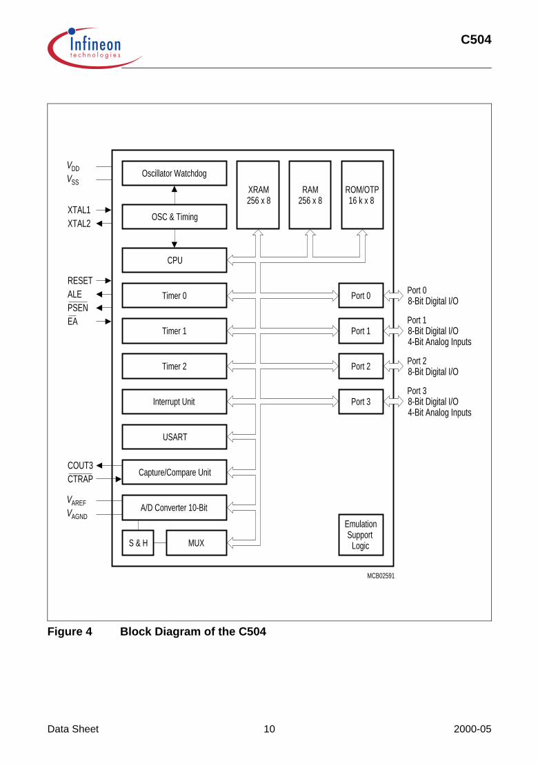
Figure 4 Block Diagram of the C504
MCB02591
Oscillator Watchdog
OSC & Timing
CPU
Timer 1
Timer 2
Interrupt Unit
USART
Capture/Compare Unit
A/D Converter 10-Bit
Timer 0
S & H MUX
XRAM256 x 8RAM ROM/OTP
16 k x 8
Port 0
Port 1
Port 2
Port 3
Port 0
Port 1
Port 2
Port 3
XTAL2XTAL1
VDD
SSV
RESETALEPSENEA
COUT3CTRAP
VAGND
AREFV
8-Bit Digital I/O4-Bit Analog Inputs
8-Bit Digital I/O
8-Bit Digital I/O
4-Bit Analog Inputs8-Bit Digital I/O
SupportEmulation
Logic
256 x 8
Data Sheet 10 2000-05

C504
CPU
The C504 is efficient both as a controller and as an arithmetic processor. It has extensivefacilities for binary and BCD arithmetic and excels in its bit-handling capabilities. Efficientuse of program memory results from an instruction set consisting of 44% one-byte, 41%two-byte, and 15% three-byte instructions. With a 12 MHz crystal, 58% of the instructionsare executed in 1.0 µs (24 MHz: 500 ns, 40 MHz: 300 ns).
Special Function Register PSW (Address D0H) Reset Value: 00H
Bit Function
CY Carry FlagUsed by arithmetic instructions.
AC Auxiliary Carry FlagUsed by instructions which execute BCD operations.
F0 General Purpose Flag 0
RS1RS0
Register Bank Select Control bitsThese bits are used to select one of the four register banks.
OV Overflow FlagUsed by arithmetic instruction.
F1 General Purpose Flag 1
P Parity FlagSet/cleared by hardware after each instruction to indicate an odd/even number of “one” bits in the accumulator.
CY AC F0 RS1 RS0 OV F1 PD0H PSW
D7H D6H D5H D4H D3H D2H D1H D0H
Bit No. MSB LSB
RS1 RS0 Function
0 0 Bank 0 selected, data address 00H-07H
0 1 Bank 1 selected, data address 08H-0FH
1 0 Bank 2 selected, data address 10H-17H
1 1 Bank 3 selected, data address 18H-1FH
Data Sheet 11 2000-05

C504
Memory Organization
The C504 CPU manipulates operands in the following four address spaces:
– up to 64 Kbyte of program memory: 16K ROM for C504-2R16K OTP for C504-2E
– up to 64 Kbyte of external data memory– 256 bytes of internal data memory– 256 bytes of internal XRAM data memory– a 128 byte special function register area
Figure 5 illustrates the memory address spaces of the C504.
Figure 5 C504 Memory Map
MCD02592
00H
H7F
0000 H
3FFFH
External
FFFF H
H4000
(EA = 0)(EA = 1)
"Code Space" "Data Space" "Internal Data Space"
H0000
HFFFF
External
FF00 HFEFFH
InternalXRAM
RAMInternalInternal External
InternalRAM
FFH
H80
FunctionSpecial
Register
DirectAddress
80H
HFFAddressIndirect
Data Sheet 12 2000-05
C504
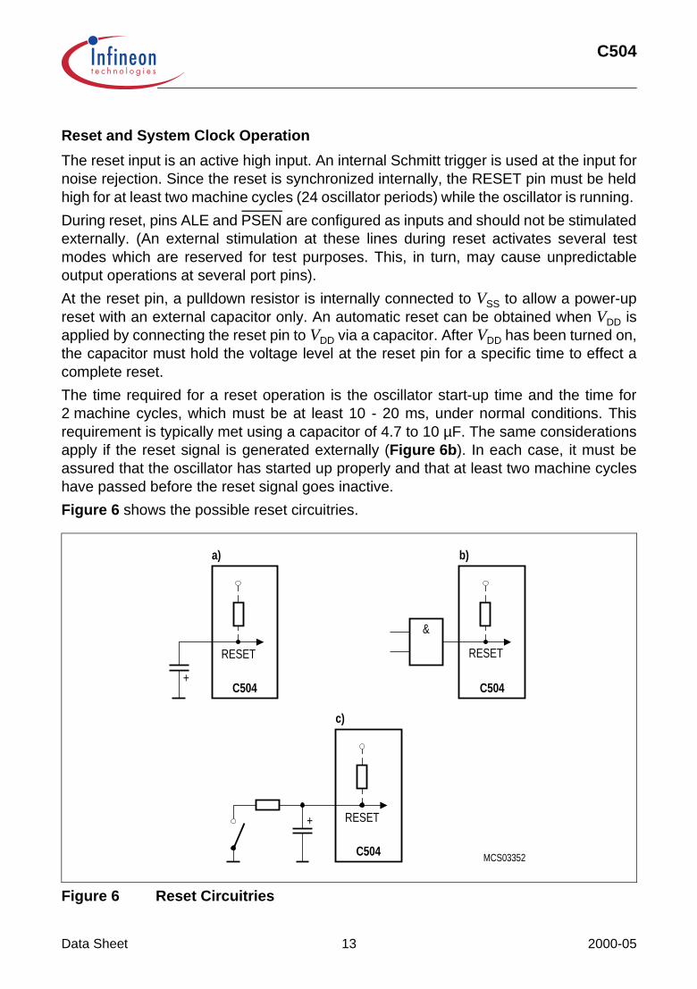
Reset and System Clock Operation
The reset input is an active high input. An internal Schmitt trigger is used at the input fornoise rejection. Since the reset is synchronized internally, the RESET pin must be heldhigh for at least two machine cycles (24 oscillator periods) while the oscillator is running.
During reset, pins ALE and PSEN are configured as inputs and should not be stimulatedexternally. (An external stimulation at these lines during reset activates several testmodes which are reserved for test purposes. This, in turn, may cause unpredictableoutput operations at several port pins).
At the reset pin, a pulldown resistor is internally connected to VSS to allow a power-upreset with an external capacitor only. An automatic reset can be obtained when VDD isapplied by connecting the reset pin to VDD via a capacitor. After VDD has been turned on,the capacitor must hold the voltage level at the reset pin for a specific time to effect acomplete reset.
The time required for a reset operation is the oscillator start-up time and the time for2 machine cycles, which must be at least 10 - 20 ms, under normal conditions. Thisrequirement is typically met using a capacitor of 4.7 to 10 µF. The same considerationsapply if the reset signal is generated externally (Figure 6b). In each case, it must beassured that the oscillator has started up properly and that at least two machine cycleshave passed before the reset signal goes inactive.
Figure 6 shows the possible reset circuitries.
Figure 6 Reset Circuitries
a)
+
b)
+
C504
RESET
c)
&
MCS03352
C504 C504
RESET RESET
Data Sheet 13 2000-05

C504
Figure 7 shows the recommended oscillator circuit for the C504, while Figure 8 showsthe circuit for using an external clock source.
Figure 7 Recommended Oscillator Circuit
Figure 8 External Clock Source
MCS03353
C
3.5 - 40MHz
XTAL2
XTAL1
C = 20 pF 10 pF for crystal operation
C504
C
MCS03355
XTAL1
XTAL2N.C.
V DDC504
ExternalClockSignal
Data Sheet 14 2000-05
C504
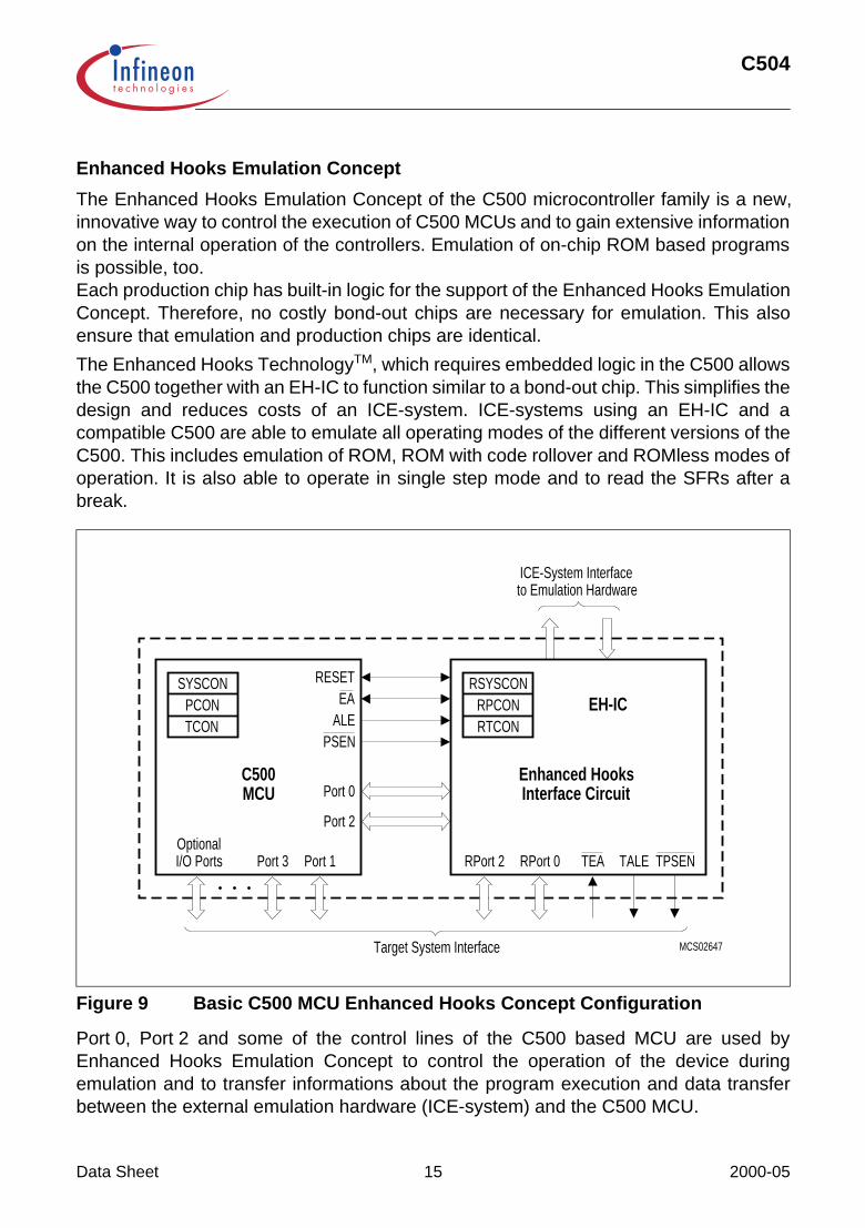
Enhanced Hooks Emulation Concept
The Enhanced Hooks Emulation Concept of the C500 microcontroller family is a new,innovative way to control the execution of C500 MCUs and to gain extensive informationon the internal operation of the controllers. Emulation of on-chip ROM based programsis possible, too.Each production chip has built-in logic for the support of the Enhanced Hooks EmulationConcept. Therefore, no costly bond-out chips are necessary for emulation. This alsoensure that emulation and production chips are identical.
The Enhanced Hooks TechnologyTM, which requires embedded logic in the C500 allowsthe C500 together with an EH-IC to function similar to a bond-out chip. This simplifies thedesign and reduces costs of an ICE-system. ICE-systems using an EH-IC and acompatible C500 are able to emulate all operating modes of the different versions of theC500. This includes emulation of ROM, ROM with code rollover and ROMless modes ofoperation. It is also able to operate in single step mode and to read the SFRs after abreak.
Figure 9 Basic C500 MCU Enhanced Hooks Concept Configuration
Port 0, Port 2 and some of the control lines of the C500 based MCU are used byEnhanced Hooks Emulation Concept to control the operation of the device duringemulation and to transfer informations about the program execution and data transferbetween the external emulation hardware (ICE-system) and the C500 MCU.
MCS02647
SYSCONPCONTCON
RESETEA
PSENALE
Port 0
Port 2
I/O PortsOptional
Port 3 Port 1
C500MCU Interface Circuit
Enhanced Hooks
RPort 0RPort 2
RTCONRPCON
RSYSCON
TEA TALE TPSEN
EH-IC
Target System Interface
ICE-System Interfaceto Emulation Hardware
Data Sheet 15 2000-05

C504
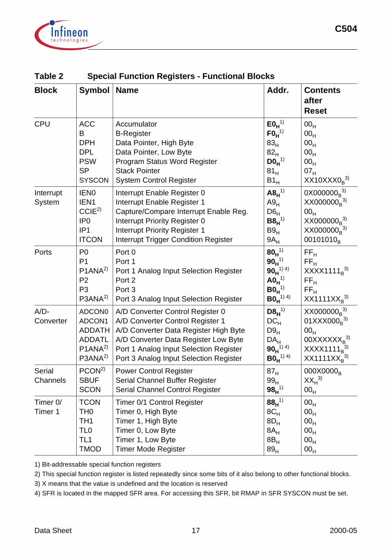
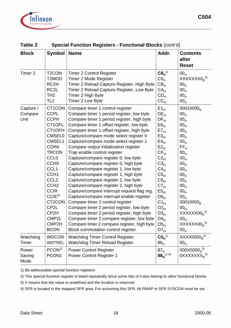
Special Function Registers
All registers, except the program counter and the four general purpose register banks,reside in the special function register area.
The 63 special function registers (SFR) include pointers and registers that provide aninterface between the CPU and the other on-chip peripherals. All SFRs with addresseswhere address bits 0-2 are 0 (e.g. 80H, 88H, 90H, 98H, …, F0H, F8H) are bit-addressable.
The SFRs of the C504 are listed in Table 2 and Table 3. In Table 2, they are organizedin groups which refer to the functional blocks of the C504. Table 3 illustrates the contentsof the SFRs in numeric order of their addresses.
Data Sheet 16 2000-05
C504
Table 2 Special Function Registers - Functional Blocks
Block Symbol Name Addr. Contents afterReset
CPU ACCBDPHDPLPSWSPSYSCON
AccumulatorB-RegisterData Pointer, High ByteData Pointer, Low ByteProgram Status Word RegisterStack PointerSystem Control Register
E0H1)
F0H1)
83H
82H
D0H1)
81H
B1H
00H
00H
00H
00H
00H
07H
XX10XXX0B3)
InterruptSystem
IEN0IEN1CCIE2)
IP0IP1ITCON
Interrupt Enable Register 0Interrupt Enable Register 1Capture/Compare Interrupt Enable Reg. Interrupt Priority Register 0Interrupt Priority Register 1Interrupt Trigger Condition Register
A8H1)
A9H
D6H
B8H1)
B9H
9AH
0X000000B3)
XX000000B3)
00H
XX000000B3)
XX000000B3)
00101010B
Ports P0P1P1ANA2)
P2P3P3ANA2)
Port 0Port 1Port 1 Analog Input Selection RegisterPort 2Port 3Port 3 Analog Input Selection Register
80H1)
90H1)
90H1) 4)
A0H1)
B0H1)
B0H1) 4)
FFH
FFH
XXXX1111B3)
FFH
FFH
XX1111XXB3)
A/D-Converter
ADCON0ADCON1ADDATHADDATLP1ANA2)
P3ANA2)
A/D Converter Control Register 0A/D Converter Control Register 1A/D Converter Data Register High ByteA/D Converter Data Register Low BytePort 1 Analog Input Selection RegisterPort 3 Analog Input Selection Register
D8H1)
DCH
D9H
DAH
90H1) 4)
B0H1) 4)
XX000000B3)
01XXX000B3)
00H
00XXXXXXB3)
XXXX1111B3)
XX1111XXB3)
SerialChannels
PCON2)
SBUFSCON
Power Control RegisterSerial Channel Buffer RegisterSerial Channel Control Register
87H
99H
98H1)
000X0000B
XXH3)
00H
Timer 0/Timer 1
TCONTH0TH1TL0TL1TMOD
Timer 0/1 Control RegisterTimer 0, High ByteTimer 1, High ByteTimer 0, Low ByteTimer 1, Low ByteTimer Mode Register
88H1)
8CH
8DH
8AH
8BH
89H
00H
00H
00H
00H
00H
00H
1) Bit-addressable special function registers
2) This special function register is listed repeatedly since some bits of it also belong to other functional blocks.
3) X means that the value is undefined and the location is reserved
4) SFR is located in the mapped SFR area. For accessing this SFR, bit RMAP in SFR SYSCON must be set.
Data Sheet 17 2000-05
C504
Timer 2 T2CONT2MODRC2HRC2LTH2TL2
Timer 2 Control RegisterTimer 2 Mode RegisterTimer 2 Reload Capture Register, High ByteTimer 2 Reload Capture Register, Low ByteTimer 2 High ByteTimer 2 Low Byte
C8H1)
C9H
CBH
CAH
CDH
CCH
00H
XXXXXXX0B3)
00H
00H
00H
00H
Capture /CompareUnit
CT1CONCCPLCCPHCT1OFLCT1OFHCMSEL0CMSEL1COINITRCONCCL0CCH0CCL1CCH1CCL2CCH2CCIRCCIE2)
CT2CONCP2LCP2HCMP2LCMP2HBCON
Compare timer 1 control registerCompare timer 1 period register, low byteCompare timer 1 period register, high byteCompare timer 1 offset register, low byteCompare timer 1 offset register, high byteCapture/compare mode select register 0Capture/compare mode select register 1Compare output initialization registerTrap enable control registerCapture/compare register 0, low byteCapture/compare register 0, high byteCapture/compare register 1, low byteCapture/compare register 1, high byteCapture/compare register 2, low byteCapture/compare register 2, high byteCapture/compare interrupt request flag reg.Capture/compare interrupt enable registerCompare timer 2 control registerCompare timer 2 period register, low byteCompare timer 2 period register, high byteCompare timer 2 compare register, low byteCompare timer 2 compare register, high byteBlock commutation control register
E1HDEHDFHE6HE7HE3HE4HE2HCFHC2HC3HC4HC5HC6HC7HE5HD6HC1HD2HD3HD4HD5HD7H
00010000B
00H
00H
00H
00H
00H
00H
FFH
00H
00H
00H
00H
00H
00H
00H
00H
00H
00010000B
00H
XXXXXX00B3)
00H
XXXXXX00B3)
00H
WatchdogTimer
WDCONWDTREL
Watchdog Timer Control RegisterWatchdog Timer Reload Register
C0H1)
86H
XXXX0000B3)
00H
Power Saving Mode
PCON2)
PCON1Power Control RegisterPower Control Register 1
87H
88H1) 4)
000X0000B3)
0XXXXXXXB3)
1) Bit-addressable special function registers
2) This special function register is listed repeatedly since some bits of it also belong to other functional blocks.
3) X means that the value is undefined and the location is reserved
4) SFR is located in the mapped SFR area. For accessing this SFR, bit RMAP in SFR SYSCON must be set.
Table 2 Special Function Registers - Functional Blocks (cont’d)
Block Symbol Name Addr. Contents afterReset
Data Sheet 18 2000-05

C504
Table 3 Contents of the SFRs, SFRs in Numeric Order of their Addresses
Addr Register Contentafter Reset1)
Bit 7 Bit 6 Bit 5 Bit 4 Bit 3 Bit 2 Bit 1 Bit 0
80H2) P0 FFH .7 .6 .5 .4 .3 .2 .1 .0
81H SP 07H .7 .6 .5 .4 .3 .2 .1 .0
82H DPL 00H .7 .6 .5 .4 .3 .2 .1 .0
83H DPH 00H .7 .6 .5 .4 .3 .2 .1 .0
86H WDTREL 00H WDTPSEL
.6 .5 .4 .3 .2 .1 .0
87H PCON 000X-0000B
SMOD PDS IDLS – GF1 GF0 PDE IDLE
88H2) TCON 00H TF1 TR1 TF0 TR0 IE1 IT1 IE0 IT0
88H1)3) PCON1 0XXX-
XXXXB
EWPD – – – – – – –
89H TMOD 00H GATE C/T M1 M0 GATE C/T M1 M0
8AH TL0 00H .7 .6 .5 .4 .3 .2 .1 .0
8BH TL1 00H .7 .6 .5 .4 .3 .2 .1 .0
8CH TH0 00H .7 .6 .5 .4 .3 .2 .1 .0
8DH TH1 00H .7 .6 .5 .4 .3 .2 .1 .0
90H2) P1 FFH .7 .6 .5 .4 .3 .2 T2EX T2
90H2)3) P1ANA XXXX-
1111B
– – – – EAN3 EAN2 EAN1 EAN0
98H2) SCON 00H SM0 SM1 SM2 REN TB8 RB8 TI RI
99H SBUF XXH .7 .6 .5 .4 .3 .2 .1 .0
9AH ITCON 0010-1010B
IT2 IE2 I2ETF I2ETR I1ETF I1ETR I0ETF I0ETR
A0H2) P2 FFH .7 .6 .5 .4 .3 .2 .1 .0
A8H2) IEN0 0X00-
0000B
EA – ET2 ES ET1 EX1 ET0 EX0
A9H IEN1 XX00-0000B
– – ECT1 ECCM ECT2 ECEM EX2 EADC
1) X means that the value is undefined and the location is reserved2) Bit-addressable special function registers3) SFR is located in the mapped SFR area. For accessing this SFR, bit RMAP in SFR SYSCON must be set.
Data Sheet 19 2000-05

C504
B0H2) P3 FFH RD WR T1 T0 INT1 INT0 TxD RxD
B0H2)3) P3ANA XX11-
11XXB
– – EAN7 EAN6 EAN5 EAN4 – –
B1H SYSCON XX10-XXX0B
– – EALE RMAP – – – XMAP
B8H2) IP0 XX00-
0000B
– – PT2 PS PT1 PX1 PT0 PX0
B9H IP1 XX00-0000B
– – PCT1 PCCM PCT2 PCEM PX2 PADC
C0H2) WDCON XXXX-
0000B
– – – – OWDS WDTS WDT SWDT
C1H CT2CON 0001-0000B
CT2P ECT2O STE2 CT2RES
CT2R CLK2 CLK1 CLK0
C2H CCL0 00H .7 .6 .5 .4 .3 .2 .1 .0
C3H CCH0 00H .7 .6 .5 .4 .3 .2 .1 .0
C4H CCL1 00H .7 .6 .5 .4 .3 .2 .1 .0
C5H CCH1 00H .7 .6 .5 .4 .3 .2 .1 .0
C6H CCL2 00H .7 .6 .5 .4 .3 .2 .1 .0
C7H CCH2 00H .7 .6 .5 .4 .3 .2 .1 .0
C8H2) T2CON 00H TF2 EXF2 RCLK TCLK EXEN2 TR2 C/T2 CP/
RL2
C9H T2MOD XXXX-XXX0B
– – – – – – – DCEN
CAH RC2L 00H .7 .6 .5 .4 .3 .2 .1 .0
CBH RC2H 00H .7 .6 .5 .4 .3 .2 .1 .0
CCH TL2 00H .7 .6 .5 .4 .3 .2 .1 .0
CDH TH2 00H .7 .6 .5 .4 .3 .2 .1 .0
CFH TRCON 00H TRPEN TRF TREN5 TREN4 TREN3 TREN2 TREN1 TREN0
1) X means that the value is undefined and the location is reserved2) Bit-addressable special function registers3) SFR is located in the mapped SFR area. For accessing this SFR, bit RMAP in SFR SYSCON must be set.
Table 3 Contents of the SFRs, SFRs in Numeric Order of their Addresses (cont’d)
Addr Register Contentafter Reset1)
Bit 7 Bit 6 Bit 5 Bit 4 Bit 3 Bit 2 Bit 1 Bit 0
Data Sheet 20 2000-05

C504
D0H2) PSW 00H CY AC F0 RS1 RS0 OV F1 P
D2H CP2L 00H .7 .6 .5 .4 .3 .2 .1 .0
D3H CP2H XXXX.XX00B
– – – – – – .1 .0
D4H CMP2L 00H .7 .6 .5 .4 .3 .2 .1 .0
D5H CMP2H XXXX.XX00B
– – – – – – .1 .0
D6H CCIE 00H ECTP ECTC CC2FEN
CC2REN
CC1FEN
CC1REN
CC0FEN
CC0REN
D7H BCON 00H BCMPBCEM
PWM1 PWM0 EBCE BCERR BCEN BCM1 BCM0
D8H2) ADCON0 XX00-
0000B
– – IADC BSY ADM MX2 MX1 MX0
D9H ADDATH 00H .9 .8 .7 .6 .5 .4 .3 .2
DAH ADDATL 00XX-XXXXB
.1 .0 – – – – – –
DCH ADCON1 01XX-X000B
ADCL1 ADCL0 – – – MX2 MX1 MX0
DEH CCPL 00H .7 .6 .5 .4 .3 .2 .1 .0
DFH CCPH 00H .7 .6 .5 .4 .3 .2 .1 .0
E0H2) ACC 00H .7 .6 .5 .4 .3 .2 .1 .0
E1H CT1CON 0001-0000B
CTM ETRP STE1 CT1RES
CT1R CLK2 CLK1 CLK0
E2H COINI FFH COUT3I
COUTXI
COUT2I
CC2I COUT1I
CC1I COUT0I
CC0I
E3H CMSEL0 00H CMSEL13
CMSEL12
CMSEL11
CMSEL10
CMSEL03
CMSEL02
CMSEL01
CMSEL00
E4H CMSEL1 00H 0 0 0 0 CMSEL23
CMSEL22
CMSEL21
CMSEL20
E5H CCIR 00H CT1FP CT1FC CC2F CC2R CC1F CC1R CC0F CC0R
E6H CT1OFL 00H .7 .6 .5 .4 .3 .2 .1 .0
E7H CT1OFH 00H .7 .6 .5 .4 .3 .2 .1 .0
F0H2) B 00H .7 .6 .5 .4 .3 .2 .1 .0
1) X means that the value is undefined and the location is reserved
2) Bit-addressable special function registers
Table 3 Contents of the SFRs, SFRs in Numeric Order of their Addresses (cont’d)
Addr Register Contentafter Reset1)
Bit 7 Bit 6 Bit 5 Bit 4 Bit 3 Bit 2 Bit 1 Bit 0
Data Sheet 21 2000-05

C504
Timer/Counter 0 and 1
Timer/Counter 0 and 1 can be used in four operating modes as listed in Table 4.
In the “timer” function (C/T = ‘0’), the register is incremented every machine cycle.Therefore the count rate is fOSC/12.
In the “counter” function the register is incremented in response to a 1-to-0 transition atits corresponding external input pin (P3.4/T0, P3.5/T1). Since it takes two machinecycles to detect a falling edge the max. count rate is fOSC/24. External inputs INT0 andINT1 (P3.2, P3.3) can be programmed to function as a gate to facilitate pulse widthmeasurements. Figure 10 illustrates the input clock logic.
Figure 10 Timer/Counter 0 and 1 Input Clock Logic
Table 4 Timer/Counter 0 and 1 Operating Modes
Mode Description TMOD Input Clock
Gate C/T M1 M0 internal external (max.)
0 8-bit timer/counter with a divide-by-32 prescaler
X X 0 0 fOSC/12 × 32 fOSC/24 × 32
1 16-bit timer/counter X X 1 1 fOSC/12 fOSC/24
2 8-bit timer/counter with8-bit auto-reload
X X 0 0 fOSC/12 fOSC/24
3 Timer/counter 0 used as one 8-bit timer/counter and one 8-bit timerTimer 1 stops
X X 1 1 fOSC/12 fOSC/24
12 f OSC/12
MCS01768
OSCf
C/T
TMOD
0
Control
Timer 0/1Input Clock
TCON
TR 0/1
Gate
TMOD
&
=1
1
P3.4/T0P3.5/T1max
P3.2/INT0P3.3/INT1
OSC/24f 1
÷
_<
Data Sheet 22 2000-05

C504
Timer/Counter 2
Timer 2 is a 16-bit Timer/Counter with an up/down count feature. It can operate either asa timer or as an event counter. This is selected by bit C/T2 of SFR T2CON. It has threeoperating modes as shown in Table 5.
Note: ↓ = falling edge
Table 5 Timer/Counter 2 Operating Modes
Mode T2CON T2MOD
DCEN
T2CON
EXEN
P1.1/T2EX
Remarks Input Clock
R×CLKorT×CLK
CP/RL2
TR2 internal external(P1.0/T2)
16-bitAuto-reload
0
0
00
0
0
00
1
1
11
0
0
11
0
1
XX
X
↓
01
reload upon overflow reload trigger(falling edge)Down countingUp counting
fOSC/12 maxfOSC/24
16-bitCap-ture
0
0
1
1
1
1
X
X
0
1
X
↓
16 bit Timer/Counter (only up-counting)capture TH2, TL2 → RC2H, RC2L
fOSC/12 maxfOSC/24
BaudRateGene-rator
1
1
X
X
1
1
X
X
0
1
X
↓
no overflow interrupt request (TF2) extra external interrupt (“Timer 2”)
fOSC/2 maxfOSC/24
off X X 0 X X X Timer 2 stops – –
Data Sheet 23 2000-05
C504
Capture/Compare Unit
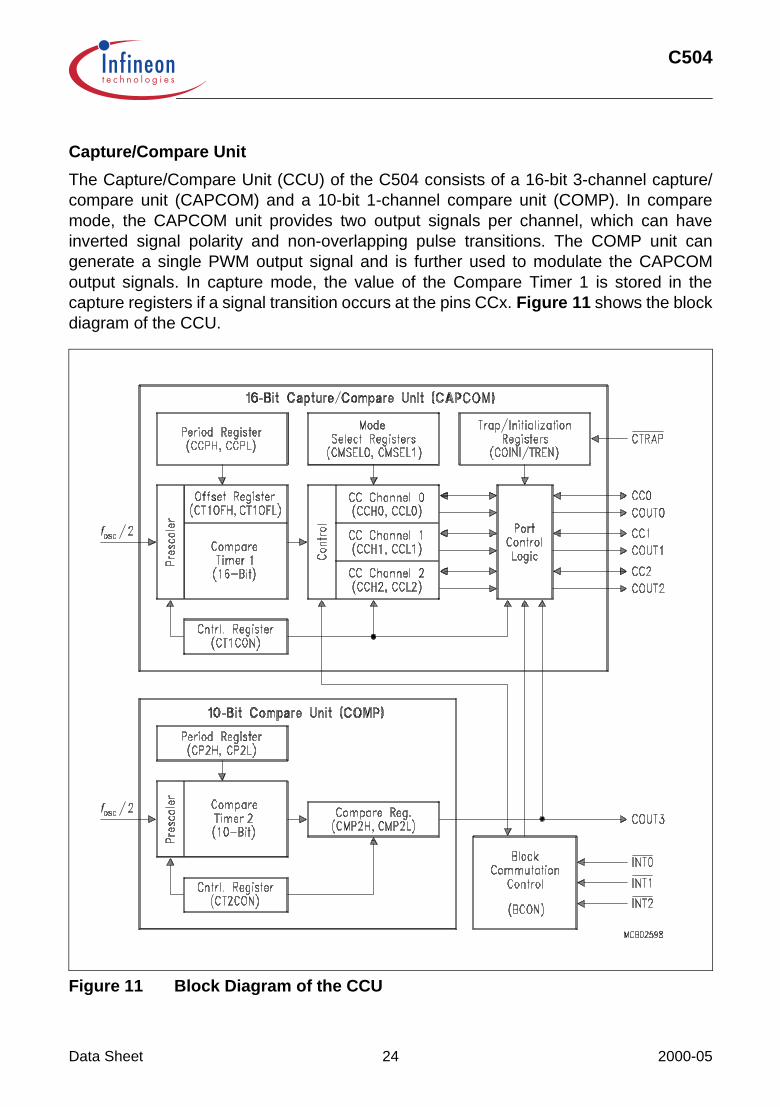
The Capture/Compare Unit (CCU) of the C504 consists of a 16-bit 3-channel capture/compare unit (CAPCOM) and a 10-bit 1-channel compare unit (COMP). In comparemode, the CAPCOM unit provides two output signals per channel, which can haveinverted signal polarity and non-overlapping pulse transitions. The COMP unit cangenerate a single PWM output signal and is further used to modulate the CAPCOMoutput signals. In capture mode, the value of the Compare Timer 1 is stored in thecapture registers if a signal transition occurs at the pins CCx. Figure 11 shows the blockdiagram of the CCU.
Figure 11 Block Diagram of the CCU
Data Sheet 24 2000-05

C504
The Compare Timers 1 and 2 are free running, processor clock coupled 16-bit / 10-bittimers; each of which has a count rate with a maximum of fOSC/2 up to fOSC/256. Thecompare timer operations with its possible compare output signal waveforms are shownin Figure 12.
Figure 12 Basic Operating Modes of the CAPCOM Unit
Compare Timer 1 can be programmed for both operating modes while Compare Timer 2works only in operating mode 0 with one output signal of selectable polarity at the pinCOUT3.
PeriodValue
ValueCompare
0000 H
CC
COUT
Value
CompareValue
Period
Offset
OFFt
ValueCompare
0000 H
ValuePeriod
CompareValue
Offset
ValuePeriod
OFFt
COINI=0
COINI=1
OFFt
: Interrupts can be generated MCT03356
Compare Timer 1 in Operating Mode 0
a) Standard PWM (Edge Aligned)
Compare Timer 1 in Operating Mode 1
b) Standard PWM (Single Edge Aligned)with programmable dead time ( )OFFt
Symetrical PWM (Center Aligned)c)with programmable dead time ( )Symetrical PWM (Center Aligned)d)
OFFt
CC
COUT
COINI=0
COINI=1
CC
COUT
CC
COUT
Data Sheet 25 2000-05

C504
Serial Interface (USART)
The serial port is full duplex and can operate in four modes (one synchronous mode,three asynchronous modes) as illustrated in Table 6. The possible baud rates can becalculated using the formulas given in Table 6.
Figure 13 Baud Rate Generation for the Serial Interface
Table 6 USART Operating Modes
Mode SCON Baud Rate Description
SM0 SM1
0 0 0 fOSC/12 Serial data enters and exits through R×D. T×D outputs the shift clock. 8-bit are transmitted/received (LSB first)
1 0 1 Timer 1/2 overflow rate 8-bit UART10 bits are transmitted (through T×D) or received (R×D)
2 1 0 fOSC/32 or fOSC/64 9-bit UART11 bits are transmitted (T×D) orreceived (R×D)
3 1 1 Timer 1/2 overflow rate 9-bit UARTLike mode 2 except the variable baud rate
2
SM0 / SM1 PCON.7(SMOD) (RCLK, TCLK)
T2CONTimer 1Overflow
Phase 2CLK(= /2)f OSC
Timer 2Overflow
Mode 1, 3
Mode 2
0 0
1 1
MCB02414
BaudRateClock
Data Sheet 26 2000-05

C504
The possible baud rates can be calculated using the formulas given in Table 7.
Table 7 Formulas for Calculating Baud Rates
Source of Baud Rate
Operating Mode Baud Rate
Oscillator 02
fOSC/12(2SMOD × fOSC)/64
Timer 1 (16-bit timer)(8-bit timer with8-bit auto-reload)
1, 31, 3
(2SMOD × timer 1 overflow rate)/32(2SMOD × fOSC)/(32 × 12 × (256-TH1))
Timer 2 1, 3 fOSC/(32 × (65536-(RC2H, RC2L))
Data Sheet 27 2000-05

C504
10-Bit A/D Converter
The C504 has a high performance 8-channel 10-bit A/D converter using successiveapproximation technique for the conversion of analog input voltages. Figure 14 showsthe block diagram of the A/D Converter.
Figure 14 A/D Converter Block Diagram
ADDATLADDATH
Shaded bit locations are not used in ADC-functions.
AREF
AGNDVV
OSCf /2÷ 32, 16, 8, 4PrescalerClock
Port 1/3
Conversion
Write toADDATL
MCB02616
BusInternal
ContinuousSingle/
A/D Converter
INInput Clock
Conversion Clock
f
ADCf
MUX S & H
Mode
LSB.8
Start of
MSB .1
.6
.7
.4
.5
.2
.3
(D9 )H
------
H(DA )
IEN1 (A9 )
ADCON0 (D8 )
ADCL1
ADCON1 (DC )
P3ANA (B0 )
P1ANA (90 )
-
-
-
-
H
BSY- IADC
H
ADM MX2
EAN6
ADCL0
H
-
-
EAN7
H
- -
EAN5
- - MX2
EAN4
EAN3- EAN2
MX1 MX0
MX1
-
MX0
-
EAN0EAN1
ECCM-
H
ECT1 ECT2 ECEM EADCEX2
BusInternal
Data Sheet 28 2000-05

C504
The A/D Converter uses two clock signals for operation: the conversion clock fADC (= 1/tADC) and the input clock fIN (= 1/tIN). Both clock signals are derived from the C504 systemclock fOSC which is applied at the XTAL pins. The duration of an A/D conversion is amultiple of the period of the fIN clock signal. The table in Figure 15 shows the prescalerratios and the resulting A/D conversion times which must be selected for typical systemclock rates.
Figure 15 A/D Converter Clock Selection
The analog inputs are located at Port 1 and Port 3 (4 lines on each port). Thecorresponding Port 1 and Port 3 pins have a port structure, which allows the pins to beused either as digital I/Os or analog inputs. The analog input function of these mixeddigital/analog port lines is selected via the registers P1ANA and P3ANA.
MCU System Clock Rate (fOSC)
fIN
[MHz]
Prescaler fADC
[MHz]
A/D Conversion Time [µs]
Ratio ADCL1 ADCL0
3.5 MHz 1.75 ÷ 4 0 0 .438 48 × tIN = 27.4
12 MHz 6 ÷ 4 0 0 1.5 48 × tIN = 8
16 MHz 8 ÷ 4 0 0 2 48 × tIN = 6
24 MHz 12 ÷ 8 0 1 1.5 96 × tIN = 8
32 MHz 16 ÷ 8 0 1 2 96 × tIN = 6
40 MHz 20 ÷ 16 1 0 1.25 192 × tIN = 9.6
Data Sheet 29 2000-05

C504
Interrupt System
The C504 provides 12 interrupt sources with two priority levels. Figures 16 and 17 givea general overview of the interrupt sources and illustrate the interrupt request and controlflags.
Figure 16 Interrupt Request Sources (Part 1)
Data Sheet 30 2000-05

C504
Figure 17 Interrupt Request Sources (Part 2)
MCB02596
ITCON.7IT2
P3.6/WR/INT2
ITCON.4
ITCON.5
1
EX2
IE2
IEN1.1
ITCON.6004B H
Low Priority
High Priority
IP1.1PX2
CC0RCC0REN
CCIE0.0
1
CCIR.0
CCIR.1CCIE0.1
CC0FENCC0F
CC1FCC1FEN
CCIE0.3CCIR.3
CCIR.2CCIE0.2
CC1RENCC1R
CC2FCC2FEN
CCIE0.5CCIR.5
CCIR.4CCIE0.4
CC2RENCC2R
PCCMIP1.4
H0063
IEN1.4ECCM
CCIR.7
CCIE.7
CT1FP
ECTP
ECTC
CT1FC
CCIE.6
CCIR.6
1
ECT1IEN1.5
006B H
IP1.5PCT1
PCT2IP1.3
H005B
IEN1.3ECT2
CT2P
CT2CON.7
PCEMIP1.2
H0053
IEN1.2ECEM
1
BCON.3
BCERR
EBCE
ETRP
TRF
CT1CON.6
TRCON.6
BCON.4
EA
P1.2/AN2/CC0
P1.4/CC1
P1.6/CC2
Capt
ure/
Com
pare
Mat
ch In
terru
pt
Compare Timer 1Interrupt
InterruptCompare Timer 2
InterruptCCU Emergency
Bit addressable
Request Flag iscleared by hardware IEN0.7
_<
<_
<_
_<
Data Sheet 31 2000-05

C504
A low-priority interrupt can itself be interrupted by a high-priority interrupt, but not byanother low-priority interrupt. A high-priority interrupt cannot be interrupted by any otherinterrupt sources.
If two requests of different priority level are received simultaneously, the request ofhigher priority is serviced. If requests of the same priority are received simultaneously,an internal polling sequence determines which request is serviced. Thus within eachpriority level there is a second priority structure determined by the polling sequence asshown in Table 9.
Table 8 Interrupt Vector Addresses
Request Flags Interrupt Source Vector Address
IE0TF0IE1TF1RI + TITF2 + EXF2IADCIE2TRF, BCERRCT2PCC0F-CC2F, CC0R-CC2RCT1FP, CT1FC–
External interrupt 0Timer 0 interruptExternal interrupt 1Timer 1 interruptSerial port interruptTimer 2 interruptA/D converter interruptExternal interrupt 2CAPCOM emergency interruptCompare timer 2 interruptCapture/compare match interruptCompare timer 1 interruptPower-down interrupt
0003H000BH0013H001BH0023H002BH0043H004BH0053H005BH0063H006BH007BH
Table 9 Interrupt Source Structure
Interrupt Source Priority
External Interrupt 0Timer 0 InterruptExternal Interrupt 1Timer 1 InterruptSerial ChannelTimer 2 Interrupt
A/D ConverterExternal Interrupt 2CCU Emergency InterruptCompare Timer 2 InterruptCapture/Compare Match InterruptCompare Timer 1 Interrupt
High
Low
High Priority Low Priority
Data Sheet 32 2000-05

C504
Fail Save Mechanisms
The C504 offers enhanced fail save mechanisms, which allow an automatic recoveryfrom software or hardware failure.
– a programmable 15-bit Watchdog Timer – Oscillator Watchdog
Programmable Watchdog Timer
The Watchdog Timer in the C504 is a 15-bit timer, which is incremented by a count rateof either fCYCLE/2 or fCYCLE/32 (fCYCLE = fOSC/12). Only the upper 7 bits of the 15-bitwatchdog timer count value can be programmed. Figure 18 shows the block diagram ofthe programmable Watchdog Timer.
Figure 18 Block Diagram of the Programmable Watchdog Timer
The Watchdog Timer can be started by software (bit SWDT in SFR WDCON), but itcannot be stopped during active mode of the device. If the software fails to refresh therunning Watchdog Timer, an internal reset will be initiated. The reset cause (externalreset or reset caused by the watchdog) can be examined by software (status flag WDTSin SFR WDCON is set). A refresh of the Watchdog Timer is done by setting bits WDTand SWDT (both in SFR WDCON) consecutively.
This double instruction sequence has been implemented to increase system security.
It must be noted, however, that the Watchdog Timer is halted during the idle mode andpower down mode of the processor.
Data Sheet 33 2000-05

C504
Oscillator Watchdog
The Oscillator Watchdog of the C504 serves for three functions:
– Monitoring of the on-chip oscillator’s functionThe watchdog supervises the on-chip oscillator's frequency; if it is lower than thefrequency of an auxiliary RC oscillator, the internal clock is supplied by this RCoscillator and the C504 is brought into reset. If the failure condition disappears, theC504 executes a final reset phase of typically 1 ms in order to allow the oscillatorto stabilize; then, the Oscillator Watchdog reset is released and the part startsprogram execution again.
– Fast internal reset after power-onThe oscillator watchdog unit provides a clock supply for the reset before the on-chiposcillator has started. The Oscillator Watchdog unit also works identically to themonitoring function.
– Control of external wake-up from software power-down modeWhen the software power-down mode is terminated by a low level at pin P3.2/INT0,the Oscillator Watchdog unit ensures that the microcontroller resumes operation(execution of the power-down wake-up interrupt) with the nominal clock rate. In thepower-down mode, the RC oscillator and the on-chip oscillator are stopped. Bothoscillators are started again when power-down mode is released. When the on-chiposcillator has a higher frequency than the RC oscillator, the microcontroller startsoperation after a final delay of typically 1 ms in order to allow the on-chip oscillatorto stabilize.
Data Sheet 34 2000-05

C504
Figure 19 Block Diagram of the Oscillator Watchdog
Power Saving Modes
The C504 provides two power saving modes, the idle mode and the power down mode.
– In the idle mode, the oscillator of the C504 continues to run, but the CPU is gatedoff from the clock signal. However, the interrupt system, the serial port, the A/DConverter, and all timers with the exception of the Watchdog Timer, are furtherprovided with the clock. The CPU status is preserved in its entirety: the stackpointer, program counter, program status word, accumulator, and all other registersmaintain their data during idle mode.
– In the power down mode, the RC oscillator and the on-chip oscillator whichoperates with the XTAL pins are both stopped. Therefore all functions of themicrocontroller are stopped and only the contents of the on-chip RAM, XRAM andthe SFRs are maintained. The port pins, which are controlled by their port latches,output the values that are held by their SFRs.
Table 10 gives a general overview of the entry and exit procedures of the power savingmodes.
Data Sheet 35 2000-05

C504
If a power saving mode is terminated through an interrupt, including the external wake-up via P3.2/INT0, the microcontroller state (CPU, ports, peripherals) remains preserved.If it is terminated by a hardware reset, the microcontroller is reset to its default state.
In the power down mode of operation, VDD can be reduced to minimize powerconsumption. It must be ensured, however, that VDD is not reduced before the powerdown mode is invoked, and that VDD is restored to its normal operating level, before thepower down mode is terminated.
Table 10 Power Saving Modes Overview
Mode Entering(2-InstructionExample)
Leaving by Remarks
Idle mode ORL PCON, #01HORL PCON, #20H
Occurrence of any enabled interrupt
CPU clock is stopped;CPU maintains their data;peripheral units are active (if enabled) and provided with clock.
Hardware Reset
Power Down mode
With external wake-up capability from power down enabled
ORL SYSCON,#10HORL PCON1,#80H ANL SYSCON,#0EFH
ORL PCON,#02HORL PCON,#40H
Hardware Reset Oscillator is stopped;Contents of on-chip RAM and SFRs are maintained.
P3.2/INT0 goes low for at least10 µs.It is desired that the pin be held at high level during the power down mode entry and up to the wake-up.
With external wake-up capability from power down disabledORL PCON,#02HORL PCON,#40H
Hardware Reset
Data Sheet 36 2000-05

C504
OTP Memory Operation (C504-2E only)
The C504-2E is the OTP version of the C504 microcontroller with a 16Kbyte one-timeprogrammable (OTP) program memory. Fast programming cycles are achieved (1 bytein 100 µs) with the C504-2E. Several levels of OTP memory protection can be selectedas well.
To program the device, the C504-2E must be put into the programming mode. Typically,this is not done in-system, but in a special programming hardware. In the programmingmode, the C504-2E operates as a slave device similar to an EPROM standalonememory device and must be controlled with address/data information, control lines, andan external 11.5 V programming voltage.
Figure 20 shows the pins of the C504-2E which are required for controlling of the OTPprogramming mode.
Figure 20 C504-2E Programming Mode Configuration
PMSEL1
PMSEL0
XTAL2
XTAL1
P0.0 - 7
V SSV DD
C504-2E
MCS03360
P2.0 - 7
PALE
EA /
PROG
PRD
RESET
PSEN
PSEL
VPP
Port 2 Port 0
Data Sheet 37 2000-05

C504
Pin Configuration in Programming Mode
Figure 21 Pin Configuration of the C504-2E in Programming Mode (top view)
EA /
N.C.
D6 D7D5 A6 A5 /
A13
PSEN
A7PRO
G
A4 / A12A3 / A11
XTAL2XTAL1
N.C.
PRD
RESE
T
N.C.
N.C.
111 6
34
39
44
16
2122
MCP03361
A2 / A10A1 / A9
VV
DD
SS
A0 / A8
33 31 30 29 28 27 26 25 24 2332D4
PMSE
L0
PALE N.C.
PSEL
2 3 4 5 7 8 109
20191817
15141312
43424140
38373635
C504-2E
D3D2D1D0
N.C.N.C.
N.C.N.C.N.C.N.C.N.C.N.C.N.C.
N.C.
PMSE
L1
VPP
Data Sheet 38 2000-05

C504
Pin Definitions
Table 11 contains the functional description of all C504-2E pins which are required forOTP memory programming.
Table 11 Pin Definitions and Functions of the C504-2Ein Programming Mode
Symbol Pin No. I/O Function
P-MQFP-44
RESET 4 I ResetThis input must be at static “1” (active) level throughout the entire programming mode.
PMSEL0PMSEL1
57
II
Programming mode selection pinsThese pins are used to select the different access modes in programming mode. PMSEL1,0 must satisfy a setup time to the rising edge of PALE. When the logic level of PMSEL1,0 is changed, PALE must be at low level.
PSEL 8 I Basic programming mode selectThis input is used for the basic programming mode selection and must be switched according to Figure 22.
PRD 9 I Programming mode read strobeThis input is used for read access control for OTP memory read, version byte read, and lock bit read operations.
PALE 10 I Programming address latch enablePALE is used to latch the high address lines. The high address lines must satisfy a setup and hold time to/from the falling edge of PALE. PALE must be at low level when the logic level of PMSEL1,0 is changed.
XTAL2 14 O XTAL2 Output of the inverting oscillator amplifier.
PMSEL1 PMSEL0 Access Mode
0 0 Reserved
0 1 Read version bytes
1 0 Program/read lock bits
1 1 Program/read OTP memory byte
Data Sheet 39 2000-05

C504
XTAL1 15 I XTAL1Input to the oscillator amplifier.
VSS 16 – Ground (0 V)must be applied in programming mode.
VDD 17 – Power Supply (+ 5 V)must be applied in programming mode.
P2.0 - P2.7
18 - 25 I Address linesP2.0 - P2.7 are used as multiplexed address input lines A0 - A7 and A8 - A13. A8 - A13 must be latched with PALE.
PSEN 26 I Program store enableThis input must be at static “0” level during the whole programming mode.
PROG 27 I Programming mode write strobeThis input is used in programming mode as a write strobe for OTP memory program and lock bit write operations. During basic programming mode selection, a low level must be applied to PROG.
EA/VPP 29 – Programming VoltageThis pin must be held at 11.5 V (VPP) during programming of an OTP memory byte or lock bit. During an OTP memory read operation, this pin must be at VIH.This pin is also used for basic programming mode selection. For basic programming mode selection, a low level must be applied.
P0.7 - P0.0
30-37 I/O Data linesIn programming mode, data bytes are transferred via the bidirectional D7 - D0 data lines which are located at Port 0.
N.C. 1-3, 6,11-13, 28, 38-44
– Not ConnectedThese pins should not be connected in programming mode.
Table 11 Pin Definitions and Functions of the C504-2Ein Programming Mode (cont’d)
Symbol Pin No. I/O Function
P-MQFP-44
Data Sheet 40 2000-05

C504
Programming Mode Selection
The selection for the OTP programming mode can be separated into two different parts:
– Basic programming mode selection– Access mode selection
With basic programming mode selection, the device is put into the mode in which it ispossible to access the OTP memory through the programming interface logic. Further,after selection of the basic programming mode, OTP memory accesses are executed byusing one of the access modes. These access modes are OTP memory byte program/read, version byte read, and program/read lock byte operations.
The basic programming mode selection scheme is shown in Figure 22.
Figure 22 Basic Programming Mode Selection
MCT03362
VDD
5 V
Clock(XTAL1/XTAL2)
RESET "1"
PSEN "0"
PMSEL1,0
PROG
PRD "1"
"0"
0,1
PSEL
PALE "0"
EA/VPP
VPP
VIH0 V
Ready for accessmode selectionDuring this period signals
are not actively driven
Stable
Data Sheet 41 2000-05

C504
Lock Bits Programming / Read
The C504-2E has two programmable lock bits which, when programmed according toTable 13, provide four levels of protection for the on-chip OTP code memory.
Note: A ‘1’ means that the lock bit is unprogrammed; a ‘0’ means that lock bit isprogrammed.
Table 12 Access Modes Selection
Access Mode EA/VPP
PROG PRD PMSEL Address(Port 2)
Data(Port 0)1 0
Program OTP memory byte
VPP H H H A0 - A7A8 - A15
D0 - D7
Read OTP memory byte VIH H
Program OTP lock bits VPP H H L – D1,D0 seeTable 13
Read OTP lock bits VIH H
Read OTP version byte VIH H L H Byte addr.of version byte
D0 - D7
Table 13 Lock Bit Protection Types
Lock Bits ProtectionLevel
Protection Type
D1 D0
1 1 Level 0 The OTP lock feature is disabled. During normal operation of the C504-2E, the state of the EA pin is not latched on reset.
1 0 Level 1 During normal operation of the C504-2E, MOVC instructions executed from external program memory are disabled from fetching code bytes from internal memory. EA is sampled and latched on reset. An OTP memory read operation is only possible according to ROM/OTP verification mode 2. Further programming of the OTP memory is disabled (reprogramming security).
0 1 Level 2 Same as level 1, but also OTP memory read operation using ROM verification mode 2 is disabled.
0 0 Level 3 Same as level 2; but additionally external code execution by setting EA = low during normal operation of the C504-2E is no more possible.External code execution, which is initiated by an internal program (e.g. by an internal jump instruction above the ROM boundary), is still possible.
Data Sheet 42 2000-05

C504
Version Bytes
The C504-2E and C504-2R provide three version bytes at mapped address locationsFCH, FDH, and FEH. The information stored in the version bytes, is defined by the maskof each microcontroller step. Therefore, the version bytes can be read but not written.The three version bytes hold information as manufacturer code, device type, andstepping code.
The steppings of the C504 contain the following version byte information:
Future steppings of the C504 will typically have a different value for version byte 2.
Table 14 Content of Version Bytes
Stepping Version Byte 0, VR0 (mapped addr. FCH)
Version Byte 1, VR1 (mapped addr. FDH)
Version Byte 2, VR2 (mapped addr. FEH)
C504-2R AC-Step C5H 04H 01H
C504-2EES-AA-Step
C5H 84H 01H
C504-2EES-BB-Step
C5H 84H 04H
C504-2E CA-Step C5H 84H 09H
Data Sheet 43 2000-05

C504
Note: Stresses above those listed under “Absolute Maximum Ratings” may causepermanent damage of the device. This is a stress rating only and functionaloperation of the device at these or any other conditions above those indicated inthe operational sections of this specification is not implied. Exposure to absolutemaximum rating conditions for longer periods may affect device reliability. Duringabsolute maximum rating overload conditions (VIN > VDD or VIN < VSS) the voltageon VDD pins with respect to ground (VSS) must not exceed the values defined bythe absolute maximum ratings.
Absolute Maximum Ratings
Parameter Symbol Limit Values Unit Notes
min. max.
Storage temperature TST – 65 150 °C –
Voltage on VDD pins with respect to ground (VSS)
VDD – 0.5 6.5 V –
Voltage on any pin with respect to ground (VSS)
VIN – 0.5 VDD + 0.5 V –
Input current on any pin during overload condition
– – 10 10 mA –
Absolute sum of all input currents during overload condition
– – |100 mA| mA –
Power dissipation PDISS – 1 W –
Operating Conditions
Parameter Symbol Limit Values Unit Notes
min. max.
Supply voltage VDD 4.25 5.5 V –
Ground voltage VSS 0 V –
Ambient temperature SAB-C504 SAF-C504 SAK-C504
TATATA
0– 40– 40
7085125
°C –
Analog reference voltage VAREF 4 VDD + 0.1 V –
Analog ground voltage VAGND VSS – 0.1 VSS + 0.2 V –
Analog input voltage VAIN VAGND VAREF V –
CPU clock fCPU 1.75 20 MHz –
Data Sheet 44 2000-05

C504
Parameter Interpretation
The parameters listed in the following partly represent the characteristics of the C504and partly its demands on the system. To aid in interpreting the parameters right, whenevaluating them for a design, they are marked in column “Symbol”:
CC (Controller Characteristics):The logic of the C504 will provide signals with the respective characteristics.
SR (System Requirement):The external system must provide signals with the respective characteristics to theC504.
DC Characteristics(Operating Conditions apply)
Parameter Symbol Limit Values Unit Test Condition
min. max.
Input low voltage (except EA, RESET, CTRAP)
VIL SR – 0.5 0.2 VDD – 0.1
V –
Input low voltage (EA) VIL1 SR – 0.5 0.2 VDD – 0.3
V –
Input low voltage(RESET, CTRAP) VIL2 SR – 0.5 0.2 VDD +
0.1V –
Input high voltage (except XTAL1, RESET and CTRAP)
VIH SR 0.2 VDD + 0.9
VDD + 0.5 V 11)
Input high voltage to XTAL1 VIH1 SR 0.7 VDD VDD + 0.5 V –
Input high voltage to RESET and CTRAP VIH2 SR 0.6 VDD VDD + 0.5 V –
Output low voltage (Ports 1, 2, 3, COUT3) VOL CC – 0.45 V IOL = 1.6 mA1)
Output low voltage(Port 0, ALE, PSEN) VOL1 CC – 0.45 V IOL = 3.2 mA1)
Output high voltage(Ports 1, 2, 3)
VOH CC 2.40.9 VDD
––
V IOH = – 80 µAIOH = – 10 µA
Output high voltage (Ports 1, 3 pins in push-pull mode and COUT3)
VOH1 CC 0.9 VDD – V IOH = – 800 µA
Data Sheet 45 2000-05

C504
Output high voltage(Port 0 in external bus mode, ALE, PSEN)
VOH2 CC 2.40.9 VDD
––
V IOH = – 800 µA2)
IOH = – 80 µA2)
Logic 0 input current(Ports 1, 2, 3) IIL SR – 10 – 50 µA VIN = 0.45 V
Logical 1-to-0 transition current (Ports 1, 2, 3) ITL SR – 65 – 650 µA VIN = 2 V
Input leakage current(Port 0, EA) ILI CC – ± 1 µA 0.45 < VIN < VDD
Pin capacitance CIO CC – 10 pF fc = 1 MHz,TA = 25 °C
Overload current IOV SR – ± 5 mA 7) 8)
Programming voltage(C504-2E)
VPP SR 10.9 12.1 V 11.5 V ± 5%10)
Power Supply Current
Parameter Sym-bol
Limit Values Unit Test Condition
typ.8) max.9)
Active mode C504-2R 24 MHz40 MHz
IDD
IDD
27.443.1
35.957.2
mAmA
4)
C504-2E 24 MHz40 MHz
IDDIDD
20.931.0
27.941.5
mAmA
Idle mode C504-2R 24 MHz40 MHz
IDDIDD
14.622.4
19.331.3
mAmA
5)
C504-2E 24 MHz40 MHz
IDDIDD
12.316.1
16.120.9
mAmA
Power-down mode
C504-2R IPD 1 30 µA VDD = 2 … 5.5 V 3)
C504-2E IPD 35 60 µA
At EA/VPPin prog. mode
C504-2E IDDP – 30 mA –
DC Characteristics (cont’d)(Operating Conditions apply)
Parameter Symbol Limit Values Unit Test Condition
min. max.
Data Sheet 46 2000-05

C504
Notes:
1) Capacitive loading on Ports 0 and 2 may cause spurious noise pulses to be superimposed on the VOL of ALEand Port 3. The noise is due to external bus capacitance discharging into the Port 0 and Port 2 pins when thesepins make 1-to-0 transitions during bus operation. In the worst case (capacitive loading > 100 pF), the noisepulse on ALE line may exceed 0.8 V. In such cases, it may be desirable to qualify ALE with a Schmitt-trigger,or use an address latch with a Schmitt-trigger strobe input.
2) Capacitive loading on Ports 0 and 2 may cause the VOH on ALE and PSEN to momentarily fall below the0.9 VDD specification when the address lines are stabilizing.
3) IPD (power-down mode) is measured under following conditions:EA = Port 0 = VDD; RESET = VSS ; XTAL2 = N.C.; XTAL1 = VSS; VAGND = VSS; all other pins are disconnected.
4) IDD (active mode) is measured with:XTAL1 driven with tCLCH, tCHCL = 5 ns, VIL = VSS + 0.5 V, VIH = VDD – 0.5 V; XTAL2 = N.C.;EA = Port 0 = Port 1 = RESET = VDD; all other pins are disconnected. IDD would be slightly higher if a crystaloscillator is used (appr. 1 mA).
5) IDD (idle mode) is measured with all output pins disconnected and with all peripherals disabled;XTAL1 driven with tCLCH, tCHCL = 5 ns, VIL = VSS + 0.5 V, VIH = VDD – 0.5 V; XTAL2 = N.C.;RESET = EA = VSS; Port 0 = VDD; all other pins are disconnected;
6) Overload conditions occur if the standard operating conditions are exceeded, i.e. the voltage on any pinexceeds the specified range (i.e. VOV > VDD + 0.5 V or VOV < VSS – 0.5 V). The supply voltage VDD and VSSmust remain within the specified limits. The absolute sum of input currents on all port pins may not exceed50 mA.
7) Not 100 % tested, guaranteed by design characterization.
8) The typical IDD values are periodically measured at TA = + 25 °C and VDD = 5 V but not 100% tested.
9) The maximum IDD values are measured under worst case conditions (TA = 0 °C or – 40 °C and VDD = 5.5 V)
10)This VPP specification is valid for devices with version byte 2 = 02H or higher. Devices with version byte 2= 01H must be programmed with VPP = 12 V ± 5%.
11)For the C504-2E ES-AA-step the VIH min. for EA is 0.8 VDD.
Data Sheet 47 2000-05
C504
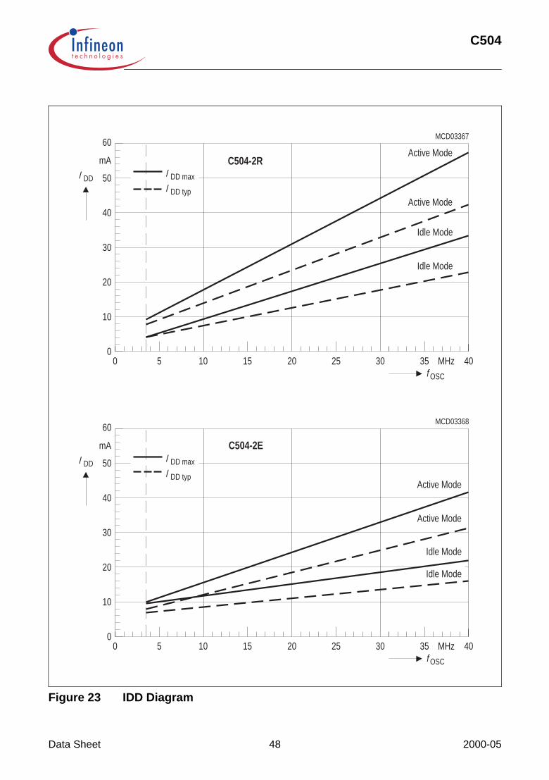
Figure 23 IDD Diagram
DDΙ
00
OSCf
MCD03368
MHz 40
mA
Active Mode
Idle Mode
DD maxΙ
DD typΙ
5 10 15 20 25
10
20
30
40
50
60
30 35
Active Mode
Idle Mode
C504-2E
DDΙ
00
OSCf
MCD03367
MHz 40
mAActive Mode
DD maxΙ
DD typΙ
5 10 15 20 25
10
20
30
40
50
60
30 35
Idle Mode
C504-2R
Active Mode
Idle Mode
Data Sheet 48 2000-05

C504
Note: fosc is the oscillator frequency in MHz. IDD values are given in mA.
Notes see next page.
Power Supply Current Calculation Formulas
Parameter Symbol Formula
Active mode C504-2R IDD typIDD max
0.98 × fOSC + 3.91.33 × fOSC + 4.0
C504-2E IDD typIDD max
0.63 × fOSC + 5.750.85 × fOSC + 7.5
Idle mode C504-2R IDD typIDD max
0.51 × fOSC + 2.350.75 × fOSC + 1.3
C504-2E IDD typIDD max
0.24 × fOSC + 6.50.30 × fOSC + 8.86
A/D Converter Characteristics(Operating Conditions apply)
Parameter Symbol Limit Values Unit Test Condition
min. max.
Analog input voltage VAIN SR VAGND VAREF V 1)
Sample time tS CC – 64 × tIN32 × tIN16 × tIN8 × tIN
ns Prescaler ÷ 32Prescaler ÷ 16Prescaler ÷ 8Prescaler ÷ 42)
Conversion cycle time tADCC CC – 384 × tIN
192 × tIN96 × tIN48 × tIN
ns Prescaler ÷ 32Prescaler ÷ 16Prescaler ÷ 8Prescaler ÷ 43)
Total unadjusted error TUE CC – ± 2 LSB VSS + 0.5 V ≤ VIN ≤ VDD – 0.5 V4)
– ± 4 LSB VSS < VIN < VSS + 0.5 VVDD – 0.5 V < VIN < VDD
4)
Internal resistance of reference voltage source
RAREF SR – tADC/250– 0.25
kΩ tADC in [ns] 5) 6)
Internal resistance of analog source
RASRCSR – tS/500– 0.25
kΩ tS in [ns] 2) 6)
ADC input capacitance CAIN CC – 50 pF 6)
Data Sheet 49 2000-05

C504
Further timing conditions: tADC min = 500 nstIN = 2/fOSC = 2 tCLCL
Notes:
1) VAIN may exceed VAGND or VAREF up to the absolute maximum ratings. However, the conversion result in thesecases will be X000H or X3FFH, respectively.
2) During the sample time, the input capacitance CAIN can be charged/discharged by the external source. Theinternal resistance of the analog source must allow the capacitance to reach their final voltage level within tS.After the end of the sample time tS, changes of the analog input voltage have no effect on the conversion result.
3) This parameter includes the sample time tS, the time for determining the digital result and the time for thecalibration. Values for the conversion clock tADC depend on programming and can be taken from the table onthe previous page.
4) TUE is tested at VAREF = 5.0 V, VAGND = 0 V, VDD = 4.9 V. It is guaranteed by design characterization for all othervoltages within the defined voltage range.If an overload condition occurs on maximum 2 not selected analog input pins and the absolute sum of inputoverload currents on all analog input pins does not exceed 10 mA, an additional conversion error of 1/2 LSBis permissible.
5) During the conversion, the ADC’s capacitance must be repeatedly charged or discharged. The internalresistance of the reference source must allow the capacitance to reach their final voltage level within theindicated time. The maximum internal resistance results from the programmed conversion timing.
6) Not 100% tested, but guaranteed by design characterization.
Clock Calculation Table
Clock Prescaler Ratio
ADCL1, 0 tADC tS tADCC
÷ 32 1 1 32 × tIN 64 × tIN 384 × tIN
÷ 16 1 0 16 × tIN 32 × tIN 192 × tIN
÷ 8 0 1 8 × tIN 16 × tIN 96 × tIN
÷ 4 0 0 4 × tIN 8 × tIN 48 × tIN
Data Sheet 50 2000-05

C504
Notes:
1) Interfacing the C504 to devices with float times up to 75 ns is permissible. This limited bus contention will notcause any damage to Port 0 drivers.
AC Characteristics for C504-L / C504-2R / C504-2E (Operating Conditions apply)(CL for Port 0, ALE and PSEN outputs = 100 pF; CL for all other outputs = 80 pF)
Parameter Symbol Limit Values Unit
12-MHz clock
Variable Clock1/tCLCL = 3.5 MHz to
12 MHz
min. max. min. max.
Program Memory Characteristics
ALE pulse width tLHLL CC 127 – 2tCLCL – 40 – ns
Address setup to ALE tAVLL CC 43 – tCLCL – 40 – ns
Address hold after ALE tLLAX CC 30 – tCLCL – 23 – ns
ALE low to valid instr in tLLIV SR – 233 – 4tCLCL – 100 ns
ALE to PSEN tLLPL CC 58 – tCLCL – 25 – ns
PSEN pulse width tPLPH CC 215 – 3tCLCL – 35 – ns
PSEN to valid instr in tPLIV SR – 150 – 3tCLCL – 100 ns
Input instruction hold after PSEN
tPXIX SR 0 – 0 – ns
Input instruction float after PSEN
tPXIZ1) SR – 63 – tCLCL – 20 ns
Address valid after PSEN tPXAV1) CC 75 – tCLCL – 8 – ns
Address to valid instr in tAVIV SR – 302 – 5tCLCL – 115 ns
Address float to PSEN tAZPL CC 0 – 0 – ns
Data Sheet 51 2000-05

C504
AC Characteristics for C504-L / C504-2R / C504-2E (cont’d)
Parameter Symbol Limit Values Unit
12-MHz clock
Variable Clock1/tCLCL = 3.5 MHz to 12 MHz
min. max. min. max.
External Data Memory Characteristics
RD pulse width tRLRH CC 400 – 6tCLCL – 100 – ns
WR pulse width tWLWH CC 400 – 6tCLCL – 100 – ns
Address hold after ALE tLLAX2 CC 114 – 2tCLCL – 53 – ns
RD to valid data in tRLDV SR – 252 – 5tCLCL – 165 ns
Data hold after RD tRHDX SR 0 – 0 – ns
Data float after RD tRHDZ SR – 97 – 2tCLCL – 70 ns
ALE to valid data in tLLDV SR – 517 – 8tCLCL – 150 ns
Address to valid data in tAVDV SR – 585 – 9tCLCL – 165 ns
ALE to WR or RD tLLWL CC 200 300 3tCLCL – 50 3tCLCL + 50 ns
Address valid to WR or RD tAVWL CC 203 – 4tCLCL – 130 – ns
WR or RD high to ALE high tWHLH CC 43 123 tCLCL – 40 tCLCL + 40 ns
Data valid to WR transition tQVWX CC 33 – tCLCL – 50 – ns
Data setup before WR tQVWH CC 433 – 7tCLCL – 150 – ns
Data hold after WR tWHQX CC 33 – tCLCL – 50 – ns
Address float after RD tRLAZ CC – 0 – 0 ns
External Clock Drive Characteristics
Parameter Symbol Limit Values Unit
Variable ClockFreq. = 3.5 MHz to 12 MHz
min. max.
Oscillator period tCLCL SR 83.3 294 ns
High time tCHCX SR 20 tCLCL – tCLCX ns
Low time tCLCX SR 20 tCLCL – tCHCX ns
Rise time tCLCH SR – 20 ns
Fall time tCHCL SR – 20 ns
Data Sheet 52 2000-05
C504
Notes:
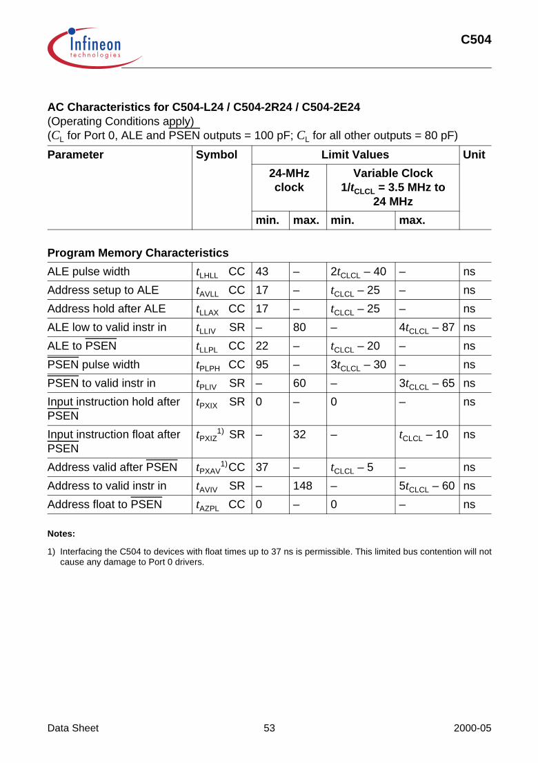
1) Interfacing the C504 to devices with float times up to 37 ns is permissible. This limited bus contention will notcause any damage to Port 0 drivers.
AC Characteristics for C504-L24 / C504-2R24 / C504-2E24(Operating Conditions apply)(CL for Port 0, ALE and PSEN outputs = 100 pF; CL for all other outputs = 80 pF)
Parameter Symbol Limit Values Unit
24-MHz clock
Variable Clock1/tCLCL = 3.5 MHz to
24 MHz
min. max. min. max.
Program Memory Characteristics
ALE pulse width tLHLL CC 43 – 2tCLCL – 40 – ns
Address setup to ALE tAVLL CC 17 – tCLCL – 25 – ns
Address hold after ALE tLLAX CC 17 – tCLCL – 25 – ns
ALE low to valid instr in tLLIV SR – 80 – 4tCLCL – 87 ns
ALE to PSEN tLLPL CC 22 – tCLCL – 20 – ns
PSEN pulse width tPLPH CC 95 – 3tCLCL – 30 – ns
PSEN to valid instr in tPLIV SR – 60 – 3tCLCL – 65 ns
Input instruction hold after PSEN
tPXIX SR 0 – 0 – ns
Input instruction float after PSEN
tPXIZ1) SR – 32 – tCLCL – 10 ns
Address valid after PSEN tPXAV1)CC 37 – tCLCL – 5 – ns
Address to valid instr in tAVIV SR – 148 – 5tCLCL – 60 ns
Address float to PSEN tAZPL CC 0 – 0 – ns
Data Sheet 53 2000-05

C504
AC Characteristics for C504-L24 / C504-2R24 / C504-2E24 (cont’d)
Parameter Symbol Limit Values Unit
24-MHz clock
Variable Clock1/tCLCL = 3.5 MHz to 24 MHz
min. max. min. max.
External Data Memory Characteristics
RD pulse width tRLRH CC 180 – 6tCLCL – 70 – ns
WR pulse width tWLWH CC 180 – 6tCLCL – 70 – ns
Address hold after ALE tLLAX2 CC 56 – 2tCLCL – 27 – ns
RD to valid data in tRLDV SR – 118 – 5tCLCL – 90 ns
Data hold after RD tRHDX SR 0 – 0 – ns
Data float after RD tRHDZ SR – 63 – 2tCLCL – 20 ns
ALE to valid data in tLLDV SR – 200 – 8tCLCL – 133 ns
Address to valid data in tAVDV SR – 220 – 9tCLCL – 155 ns
ALE to WR or RD tLLWL CC 75 175 3tCLCL – 50 3tCLCL + 50 ns
Address valid to WR tAVWL CC 67 – 4tCLCL – 97 – ns
WR or RD high to ALE high tWHLH CC 17 67 tCLCL – 25 tCLCL + 25 ns
Data valid to WR transition tQVWX CC 5 – tCLCL – 37 – ns
Data setup before WR tQVWH CC 170 – 7tCLCL – 122 – ns
Data hold after WR tWHQX CC 15 – tCLCL – 27 – ns
Address float after RD tRLAZ CC – 0 – 0 ns
External Clock Drive
Parameter Symbol Limit Values Unit
Variable ClockFreq. = 3.5 MHz to 24 MHz
min. max.
Oscillator period tCLCL SR 41.7 294 ns
High time tCHCX SR 12 tCLCL – tCLCX ns
Low time tCLCX SR 12 tCLCL – tCHCX ns
Rise time tCLCH SR – 12 ns
Fall time tCHCL SR – 12 ns
Data Sheet 54 2000-05

C504
Notes:
1) SAK-C504 is not specified for 40 MHz operation.
2) Interfacing the C504 to devices with float times up to 25 ns is permissible. This limited bus contention will notcause any damage to Port 0 drivers.
Characteristics for C504-L40 / C504-2R40 / C504-2E40(Operating Conditions apply)1)
(CL for Port 0, ALE and PSEN outputs = 100 pF; CL for all other outputs = 80 pF)
Parameter Symbol Limit Values Unit
40-MHz clock
Variable Clock1/tCLCL = 3.5 MHz to
40 MHz
min. max. min. max.
Program Memory Characteristics
ALE pulse width tLHLL CC 35 – 2tCLCL – 15 – ns
Address setup to ALE tAVLL CC 10 – tCLCL – 15 – ns
Address hold after ALE tLLAX CC 10 – tCLCL – 15 – ns
ALE low to valid instr in tLLIV SR – 55 – 4tCLCL – 45 ns
ALE to PSEN tLLPL CC 10 – tCLCL – 15 – ns
PSEN pulse width tPLPH CC 60 – 3tCLCL – 15 – ns
PSEN to valid instr in tPLIV SR – 25 – 3tCLCL – 50 ns
Input instruction hold after PSEN
tPXIX SR 0 – 0 – ns
Input instruction float after PSEN
tPXIZ2) SR – 20 – tCLCL – 5 ns
Address valid after PSEN tPXAV2) CC 20 – tCLCL – 5 – ns
Address to valid instr in tAVIV SR – 65 – 5tCLCL – 60 ns
Address float to PSEN tAZPL CC – 5 – – 5 – ns
AC
Data Sheet 55 2000-05

C504
AC Characteristics for C504-L40 / C504-2R40 / C504-2E40 (cont’d)
Parameter Symbol Limit Values Unit
40-MHz clock
Variable Clock1/tCLCL = 3.5 MHz to 40 MHz
min. max. min. max.
External Data Memory Characteristics
RD pulse width tRLRH CC 120 – 6tCLCL – 30 – ns
WR pulse width tWLWH CC 120 – 6tCLCL – 30 – ns
Address hold after ALE tLLAX2 CC 35 – 2tCLCL – 15 – ns
RD to valid data in tRLDV SR – 75 – 5tCLCL – 50 ns
Data hold after RD tRHDX SR 0 0 – ns
Data float after RD tRHDZ SR – 38 – 2tCLCL – 12 ns
ALE to valid data in tLLDV SR – 150 – 8tCLCL – 50 ns
Address to valid data in tAVDV SR – 150 – 9tCLCL – 75 ns
ALE to WR or RD tLLWL CC 60 90 3tCLCL – 15 3tCLCL + 15 ns
Address valid to WR tAVWL CC 70 – 4tCLCL – 30 – ns
WR or RD high to ALE high tWHLH CC 10 40 tCLCL – 15 tCLCL + 15 ns
Data valid to WR transition tQVWX CC 5 – tCLCL – 20 – ns
Data setup before WR tQVWH CC 125 – 7tCLCL – 50 – ns
Data hold after WR tWHQX CC 5 – tCLCL – 20 – ns
Address float after RD tRLAZ CC – 0 – 0 ns
External Clock Drive
Parameter Symbol Limit Values Unit
Variable ClockFreq. = 3.5 MHz to 40 MHz
min. max.
Oscillator period tCLCL SR 25 294 ns
High time tCHCX SR 10 tCLCL – tCLCX ns
Low time tCLCX SR 10 tCLCL – tCHCX ns
Rise time tCLCH SR – 10 ns
Fall time tCHCL SR – 10 ns
Data Sheet 56 2000-05
C504
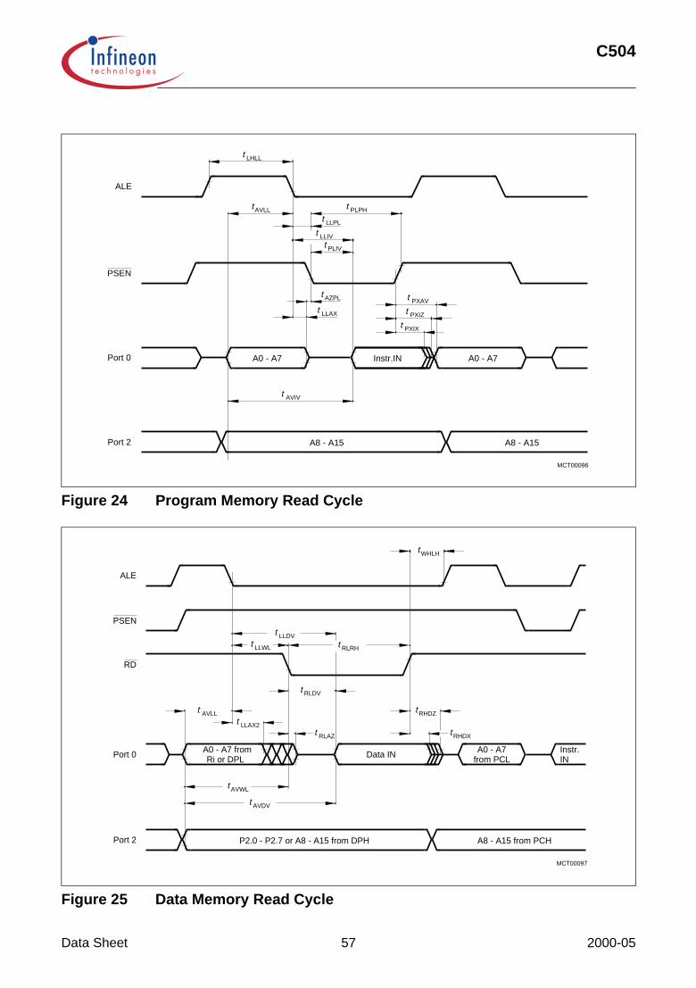
Figure 24 Program Memory Read Cycle
Figure 25 Data Memory Read Cycle
MCT00096
ALE
PSEN
Port 2
LHLLt
A8 - A15 A8 - A15
A0 - A7 Instr.IN A0 - A7Port 0
tAVLL PLPHtt LLPL
t LLIV
t PLIV
t AZPL
t LLAX t PXIZ
t PXIX
t AVIV
t PXAV
MCT00097
ALE
PSEN
Port 2
WHLHt
Port 0
RD
t LLDV
t RLRHt LLWL
t RLDV
t AVLLt LLAX2
t RLAZ
t AVWL
t AVDV
t RHDX
t RHDZ
A0 - A7 fromRi or DPL from PCL
A0 - A7 Instr.INData IN
A8 - A15 from PCHP2.0 - P2.7 or A8 - A15 from DPH
Data Sheet 57 2000-05

C504
Figure 26 Data Memory Write Cycle
Figure 27 External Clock Cycle
MCT00098
ALE
PSEN
Port 2
WHLHt
Port 0
WR
t WLWHt LLWL
tQVWX
t AVLLt LLAX2
tQVWH
t AVWL
tWHQX
A0 - A7 fromRi or DPL from PCL
A0 - A7 Instr.INData OUT
A8 - A15 from PCHP2.0 - P2.7 or A8 - A15 from DPH
MCT00033t CHCXt CLCX
CHCLtCLCHt
VDD
t CLCL
- 0.5V
0.45V
DD0.7 V
V - 0.1DD0.2
Data Sheet 58 2000-05

C504
Note:
VPP = 11.5 V ± 5% is valid for devices with version byte 2 = 02H or higher. Devices with version byte 2 = 01H must
be programmed with VPP = 12 V ± 5%.
AC Characteristics of Programming Mode (VDD = 5 V ± 10%; VPP = 11.5 V ± 5 %; TA = 25 °C ± 10 °C)
Parameter Symbol Limit Values Unit
min. max.
PALE pulse width tPAW 35 – ns
PMSEL setup to PALE rising edge tPMS 10 – ns
Address setup to PALE, PROG, or PRD falling edge
tPAS 10 – ns
Address hold after PALE, PROG, or PRD falling edge
tPAH 10 – ns
Address, data setup to PROG or PRD tPCS 100 – ns
Address, data hold after PROG or PRD tPCH 0 – ns
PMSEL setup to PROG or PRD tPMS 10 – ns
PMSEL hold after PROG or PRD tPMH 10 – ns
PROG pulse width tPWW 100 – µs
PRD pulse width tPRW 100 – ns
Address to valid data out tPAD – 75 ns
PRD to valid data out tPRD – 20 ns
Data hold after PRD tPDH 0 – ns
Data float after PRD tPDF – 20 ns
PROG high between two consecutive PROG low pulses
tPWH1 1 – µs
PRD high between two consecutive PRD low pulses
tPWH2 100 – ns
XTAL clock period tCLKP 83.3 285.7 ns
Data Sheet 59 2000-05

C504
Figure 28 Programming Code Byte - Write Cycle Timing
t PAW
t PMS
PAHtPASt
A8-A13 A0-A7
D0-D7
PCSt PWWt PCHt
t PWH
MCT03369
H, H
PALE
PMSEL1,0
Port 2
Port 0
PROG
Note: PRD must be high during a programming read cycle
Data Sheet 60 2000-05

C504
Figure 29 Verify Code Byte - Read Cycle Timing
t PAW
t PMS
PAHtPASt
A8-A13 A0-A7
PADt
D0-D7
t PDH
t PDFPRDt
PCSt PRWt PCHt
t PWH
MCT03370
H, H
PALE
PMSEL1,0
Port 2
Port 0
PRD
Note: PROG must be high during a programming read cycle
Data Sheet 61 2000-05

C504
Figure 30 Lock Bit Access Timing
Figure 31 Version Byte Read Timing
H, L H, L
D0, D1 D0, D1
t PCS
PMSt PMHt
t PCH
PWWt PMSt PRDt
t PDH
PDFt
PMHtPRWt
PMSEL1,0
Port 0
PROG
PRD
Note : PALE should be low during a lock bit read / write cycle MCT03371
e. g. FD
D0-7
t PCS
PMSt
t PDH
PDFt
PMHt
MCT03372
Port 2
Port 0
PRD
PMSEL1,0 L, H
H
PRWt
PRDt
PCHt
Note : PROG must be high during a programming read cycle
Data Sheet 62 2000-05
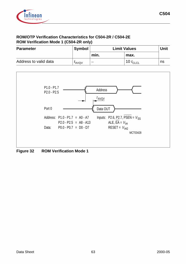
C504
Figure 32 ROM Verification Mode 1
ROM/OTP Verification Characteristics for C504-2R / C504-2EROM Verification Mode 1 (C504-2R only)
Parameter Symbol Limit Values Unit
min. max.
Address to valid data tAVQV – 10 tCLCL ns
P1.0 - P1.7P2.0 - P2.5
Port 0
Address
Data OUT
Address: P1.0 - P1.7 = A0 - A7P2.0 - P2.5 = A8 - A13
Data: P0.0 - P0.7 = D0 - D7
Inputs: P2.6, P2.7, PSEN =ALE, EA =RESET =
V SSV IH
V IH2
AVQVt
MCT03428
Data Sheet 63 2000-05

C504
Figure 33 ROM Verification Mode 2
ROM/OTP Verification Mode 2
Parameter Symbol Limit Values Unit
min. typ max.
ALE pulse width tAWD – 2 tCLCL – ns
ALE period tACY – 12 tCLCL – ns
Data valid after ALE tDVA – – 4 tCLCL ns
Data stable after ALE tDSA 8 tCLCL – – ns
P3.5 setup to ALE low tAS – tCLCL – ns
Oscillator frequency 1/tCLCL 4 – 6 MHz
MCT02613
t ACY
t AWD
t DSA
DVAt
t AS
Data Valid
ALE
Port 0
P3.5
Data Sheet 64 2000-05

C504
Figure 34 AC Testing: Input, Output Waveforms
Figure 35 AC Testing: Float Waveforms
Figure 36 Recommended Oscillator Circuits for Crystal Oscillator
AC Inputs during testing are driven at VDD – 0.5 V for a logic ‘1’ and 0.45 V for a logic ‘0’.Timing measurements are made at VIHmin for a logic ‘1’ and VILmax for a logic ‘0’.
0.45 VVDD0.2 -0.1
+0.90.2 DDV
Test Points
MCT00039
VDD -0.5 V
For timing purposes a port pin is no longer floating when a 100 mV change from load voltageoccurs and begins to float when a 100 mV change from the loaded VOH/VOL level occurs.IOL/IOH ≥ ± 20 mA
MCT00038
VLoad
VLoad -0.1 V
+0.1 VLoadV
Timing ReferencePoints
VOH -0.1 V
+0.1 VOLV
Data Sheet 65 2000-05

C504
Package Information
GP
M05
622
P-MQFP-44 (SMD)(Plastic Metric Quad Flat Package)
Sorts of PackingPackage outlines for tubes, trays etc. are contained in our Data Book “Package Information”.
Dimensions in mmSMD = Surface Mounted Device
Data Sheet 66 2000-05

Infineon goes for Business Excellence
“Business excellence means intelligent approaches and clearly defined processes, which are both constantly under review and ultimately lead to good operating results.Better operating results and business excellence mean less idleness and wastefulness for all of us, more professional success, more accurate information, a better overview and, thereby, less frustration and more satisfaction.”
Dr. Ulrich Schumacher
h t t p : / / w w w . i n f i n e o n . c o m
Published by Infineon Technologies AG