CMOS 16-BIT SINGLE CHIP MICROCOMPUTER S1C17 …€¦ · CMOS 16-BIT SINGLE CHIP MICROCOMPUTER. ......
26
Startup Manual C language S1C17 Family CMOS 16-BIT SINGLE CHIP MICROCOMPUTER
Transcript of CMOS 16-BIT SINGLE CHIP MICROCOMPUTER S1C17 …€¦ · CMOS 16-BIT SINGLE CHIP MICROCOMPUTER. ......

Startup Manual C languageS1C17 FamilyCMOS 16-BIT SINGLE CHIP MICROCOMPUTER

NOTICE No part of this material may be reproduced or duplicated in any form or by any means without the written permission of Seiko Epson. Seiko Epson reserves the right to make changes to this material without notice. Seiko Epson does not assume any liability of any kind arising out of any inaccuracies contained in this material or due to its application or use in any product or circuit and, further, there is no representation that this material is applicable to products requiring high level reliability, such as, medical products. Moreover, no license to any intellectual property rights is granted by implication or otherwise, and there is no representation or warranty that anything made in accordance with this material will be free from any patent or copyright infringement of a third party. This material or portions thereof may contain technology or the subject relating to strategic products under the control of the Foreign Exchange and Foreign Trade Law of Japan and may require an export license from the Ministry of Economy, Trade and Industry or other approval from another government agency.
All other product names mentioned herein are trademarks and/or registered trademarks of their respective companies. Windows 2000 and Windows XP are trademarks or registered trademarks of Microsoft Corporation. PC/AT and IBM are trademarks or registered trademarks of International Business Machines Corporation. All other brand and product names are trademarks or registered trademarks of respective owners.
©SEIKO EPSON CORPORATION 2008, All rights reserved.
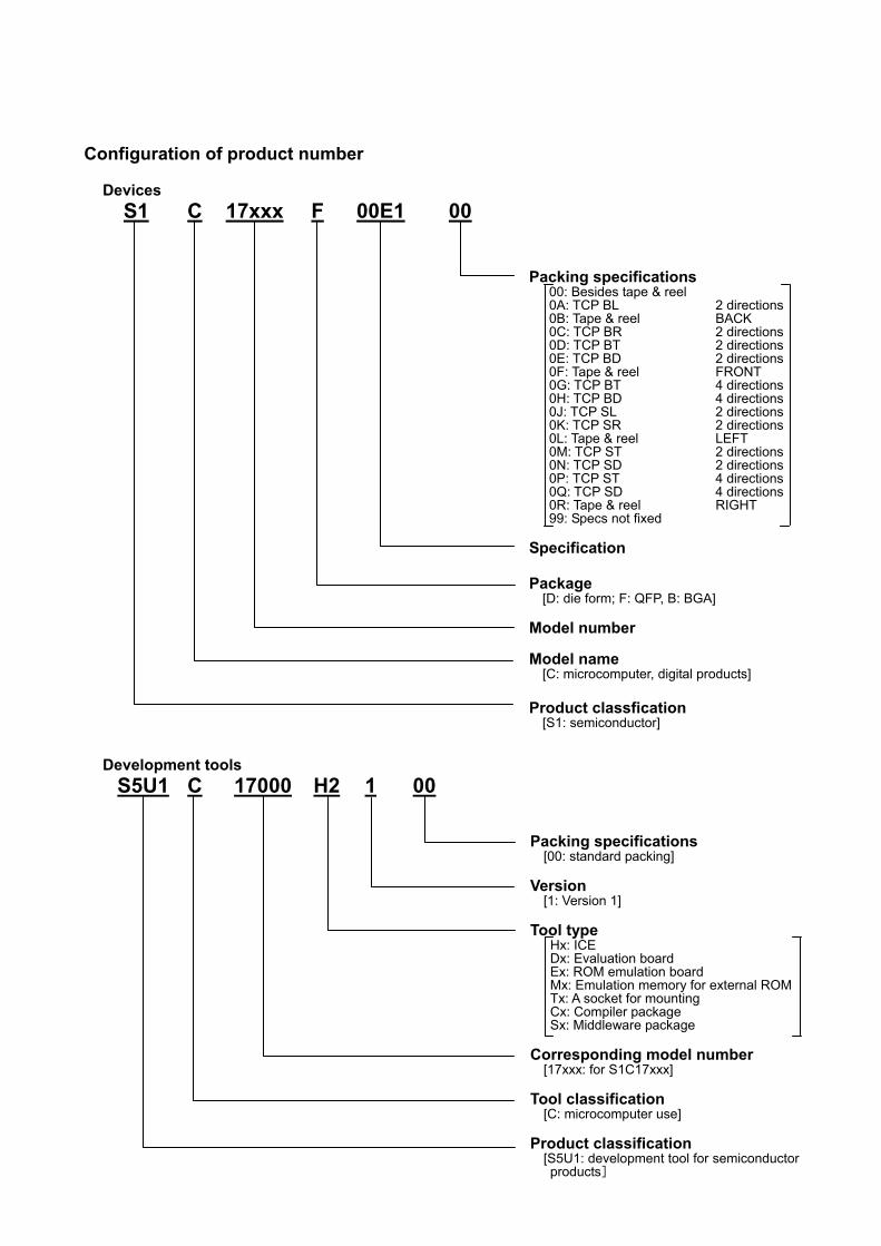
Configuration of product number
Devices
S1 C 17xxx F 00E1 00
Development tools
S5U1 C 17000 H2 1 00
Packing specifications 00: Besides tape & reel 0A: TCP BL 2 directions 0B: Tape & reel BACK 0C: TCP BR 2 directions 0D: TCP BT 2 directions 0E: TCP BD 2 directions 0F: Tape & reel FRONT 0G: TCP BT 4 directions 0H: TCP BD 4 directions 0J: TCP SL 2 directions 0K: TCP SR 2 directions 0L: Tape & reel LEFT 0M: TCP ST 2 directions 0N: TCP SD 2 directions 0P: TCP ST 4 directions 0Q: TCP SD 4 directions 0R: Tape & reel RIGHT 99: Specs not fixed
Specification Package
[D: die form; F: QFP, B: BGA] Model number Model name
[C: microcomputer, digital products] Product classfication
[S1: semiconductor]
Packing specifications [00: standard packing]
Version
[1: Version 1] Tool type
Hx: ICE Dx: Evaluation board Ex: ROM emulation board Mx: Emulation memory for external ROM Tx: A socket for mounting Cx: Compiler package Sx: Middleware package
Corresponding model number
[17xxx: for S1C17xxx] Tool classification
[C: microcomputer use] Product classification
[S5U1: development tool for semiconductor products]

- Introduction -
The S1C17 Family, 16-bit RISC Processors have various peripheral circuits including abundant interfaces that are compatible with different kinds of sensors, and the LCD driver and controller that covers wide display area. The products suitable for mobile devices are provided in this Family with high-speed operation and low power consumption. The Family has a lineup of many products with built-in Flash ROM. Rich development environment and on-chip IC function provided to the products enable customers to minimize any development period. This document has been released for an application developer who will use the S1C17 Family products, and it explains the basic embedded programming procedure of the S1C17 Family products. The reader of this document should have the following basic software knowledge.
The C language (ANSI C) and C source program creation General knowledge of the assembler language The knowledge of GNU The basic operations of the Windows 2000 or Windows XP OS
Note that sample programs given in this manual have been created by using the S1C17 Family C/C++ Compiler Package (S5U1C17001C) Version 1.2.1.
Manual Configuration: This manual consists of the following two chapters. Chapter 1 provides the basic knowledge to create an embedded software. Chapter 2 explains the basic programming procedure of the S1C17 Family products by using sample
programs. Chapter 3 explains the volatile qualifiers by the use of sample programs. Chapter 4 explains how to access I/O registers by the use of sample programs. Related Manuals:
The following lists the related manuals that you should reference to S1C17 Core Manual S5U1C17001C Manual (S1C17 Family C Compiler Package) Technical Manual for each S1C17 Family Model

S1C17 Family startup manual EPSON i C language (Rev.1.1)
Table of Contents
1. BASIC KNOWLEDGE OF EMBEDDED PROGRAMS .....................................................................1 1.1 Basic Mechanism for Program Operation ..................................................................................1 1.2 Startup (Initialize) Routine............................................................................................................2
2. PROGRAMMING OF S1C17 FAMILY PROCESSORS........................................................................3 2.1 Program Development Procedure using the GNU17 .................................................................3 2.2 Creating a Vector Table ................................................................................................................4
2.2.1 Explanation of Vector Table ......................................................................................................5 2.2.2 Relationship between Vector Table and Memory Models .........................................................6
2.3 Interrupts .......................................................................................................................................8 2.3.1 Prototype Declaration ...............................................................................................................8 2.3.2 Reset ........................................................................................................................................8 2.3.3 Address Misalignment ..............................................................................................................9 2.3.4 NMI...........................................................................................................................................9
2.4 Creating a Startup Routine.........................................................................................................10 2.4.1 Explanation of Startup Routine ............................................................................................... 11 2.4.2 Setting the SP.........................................................................................................................12 2.4.3 Initializing the .bss/.data Section ............................................................................................13 2.4.4 Enabling an Interrupt (IE) .......................................................................................................15
3. “volatile” QUALIFIER...................................................................................................16
4. HOW TO ACCESS TO I/O REGISTERS .......................................................................17 4.1 Read/Write of I/O Registers........................................................................................................17 4.2 Bit Fields......................................................................................................................................18
REVISION HISTORY.........................................................................................................19
1. BASIC KNOWLEDGE OF EMBEDDED PROGRAMS
S1C17 Family startup manual EPSON 1 C language (Rev.1.1)
1. BASIC KNOWLEDGE OF EMBEDDED PROGRAMS
This chapter is intended to be read by the user who develops an embedded software in the first time, and this chapter explains the basic concept that is very important for the user, including the basic mechanism to operate programs, system initialization by the startup routine and others.
1.1 Basic Mechanism for Program Operation
The operation when the S1C17 processor (called “the MCU” hereafter) starts, the basic operation mechanism is explained first.
Fig.1.1 Basic Mechanism during Startup of S1C17 Processor (1) When the MCU is turned ON, a Reset interrupt occurs and the MCU reads the start address of the vector
table. (2) The MCU jumps to the content (address) which was read in Step (1) and calls the Startup (Initialize)
routine. (3) The Startup routine first executes initialization that is required for stack setting and program execution. (4) When the initialization process is complete, the Startup routine calls the “main” function. Note: Addresses of various interrupt process routines are written on the Vector Table. When an interrupt
occurs, the appropriate routine address is read from the table and control jumps to the corresponding process routine.
An embedded application program must begin with the Startup routine, but not with the “main” function. The user needs to understand the Startup routine to operate the program when developing an embedded software.
(2) Jump to the startup routine (MCU interrupt processing)
(3) Process of startup routine - Sets a stack point. - Sets data required for program execution.
(4) “main” function
(1) Reset interrupt Reset vector (Start address of startup routine)
Memory Space
Application program main() {
… }
Startup routine
Interrupt vector area

1. BASIC KNOWLEDGE OF EMBEDDED PROGRAMS
2 EPSON S1C17 Family startup manual C language (Rev.1.1)
1.2 Startup (Initialize) Routine
The embedded software uses the Startup routine to execute the required initialization before executing the main routine. Generally, the following processes are executed: Setup of stack pointer Data setup required for program execution
- Clear the memory area that has no defaults. (Clearing of .bss section) - Transfer the default data from ROM area to RAM area. (Copy of .data section)
Hardware initialization and interrupt setting
Fig.1.2 Startup Routine
The “stack” is a RAM area where the current processing data, return address and others are saved temporarily when a subroutine or a function is called. As the stack is also used by the interrupt, the stack area needs to be assigned by the startup routine. When you execute the program, you need to initialize the global variables which have no defaults. Because their setting may be indefinite when reset, you need to initialize them (by clearing the .bss section). Also, if global variables have defaults, you need to copy their defaults from the ROM to RAM (by copying the .data section). In addition, you need to initialize not only the variables relating to the software execution but also the values required for MCU and other hardware operations. During interrupt setting, you also need to enable an external interrupt that can be masked. For the embedded applications, the startup routine is first executed and then the “main” function is called. You should consider these basics and develop an embedded device program.
(startup routine) START
Set the stack pointer
Initialize the .bss section.
Initialize the .data section.
Initialize the hardware and set the interrupt.
END (To the “main” function)
2. PROGRAMMING OF S1C17 FAMILY PROCESSORS
S1C17 Family startup manual EPSON 3 C language (Rev.1.1)
2. PROGRAMMING OF S1C17 FAMILY PROCESSORS
This chapter explains how to create a program that is common to the S1C17 Family processors. As explained in Chapter 1, the startup routine needs to be executed for an embedded application as the preprocessing of “main” function execution. The following gives a sample program and explains the standard process flow until you call the startup routine and the “main” function.
2.1 Program Development Procedure using the GNU17
GNU17 is the integrated program development environment that contains a series of software tools and utilities for compiling of C source programs and for assembling and debugging of assembler source programs. To install the GNU17, access to the “EPSON Microcontroller User Site” and to the “S1C17 Family” and download the “S1C17 Software Integrated Development Environment GNU17. ” The following shows the standard program development flow using the GNU17. (1) Developing a project
Develop a new project using the GNU17. (2) Creating a source program
Create a source file using the GNU17 editor or a general-purpose editor, and add this file to the project. (3) Building the program
Using GNU17, set up the startup options and linker scripts from C compiler to the linker. When you execute the build from GNU17, an elf-format object file that can be debugged and a ROM data file (psa file) which is the object file converted into S-record format.
(4) Debugging Check the program operation and debug it using the elf-format object file (created by the linker) and the S-record format ROM data file. You can set and start debugging from the GNU17.
For the detailed information, refer to the “Software Development Procedure” of the “S5U1C17001C MANUAL. ” You can find out the “S5U1C17001C MANUAL” under the “EPSON¥GNU17¥doc” directory when you have installed the GNU17.
2. PROGRAMMING OF S1C17 FAMILY PROCESSORS
4 EPSON S1C17 Family startup manual C language (Rev.1.1)
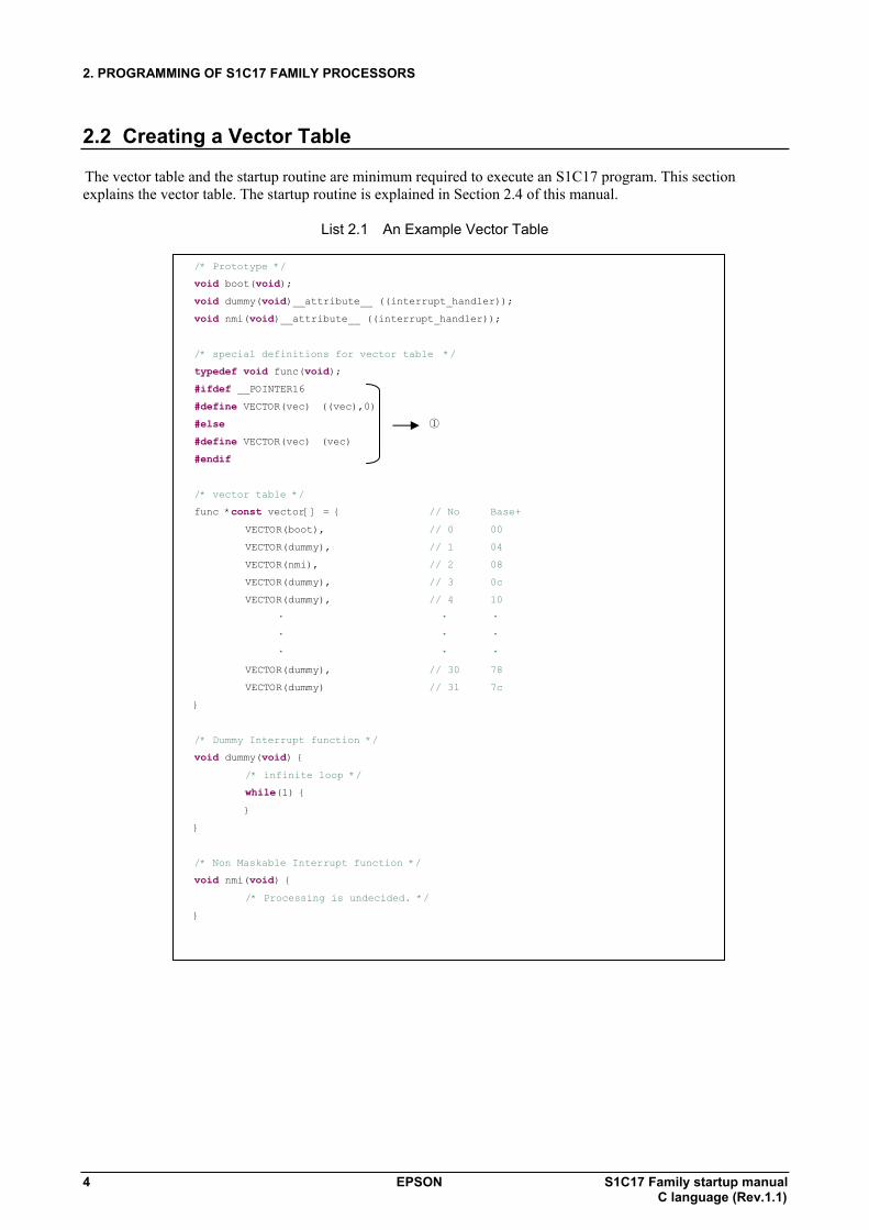
2.2 Creating a Vector Table
The vector table and the startup routine are minimum required to execute an S1C17 program. This section explains the vector table. The startup routine is explained in Section 2.4 of this manual.
List 2.1 An Example Vector Table
/* Prototype */
void boot(void); void dummy(void)__attribute__ ((interrupt_handler)); void nmi(void)__attribute__ ((interrupt_handler));
/* special definitions for vector table */
typedef void func(void); #ifdef __POINTER16 #define VECTOR(vec) ((vec),0) #else ①
#define VECTOR(vec) (vec) #endif
/* vector table */
func *const vector[] = { // No Base+
VECTOR(boot), // 0 00
VECTOR(dummy), // 1 04
VECTOR(nmi), // 2 08
VECTOR(dummy), // 3 0c
VECTOR(dummy), // 4 10
・ ・ ・
・ ・ ・
・ ・ ・
VECTOR(dummy), // 30 78
VECTOR(dummy) // 31 7c
}
/* Dummy Interrupt function */
void dummy(void) { /* infinite loop */
while(1) { }
}
/* Non Maskable Interrupt function */
void nmi(void) { /* Processing is undecided. */
}
2. PROGRAMMING OF S1C17 FAMILY PROCESSORS
S1C17 Family startup manual EPSON 5 C language (Rev.1.1)
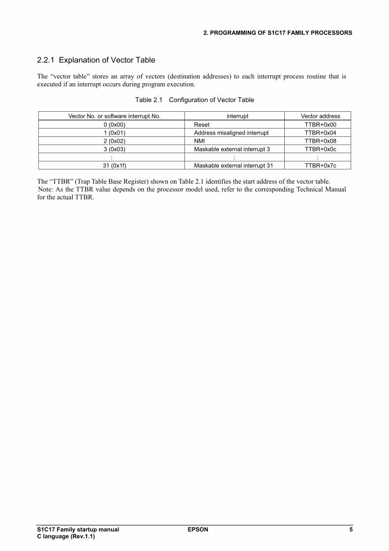
2.2.1 Explanation of Vector Table
The “vector table” stores an array of vectors (destination addresses) to each interrupt process routine that is executed if an interrupt occurs during program execution.
Table 2.1 Configuration of Vector Table
Vector No. or software interrupt No. interrupt Vector address
0 (0x00) Reset TTBR+0x00 1 (0x01) Address misaligned interrupt TTBR+0x04 2 (0x02) NMI TTBR+0x08 3 (0x03) Maskable external interrupt 3 TTBR+0x0c
: : : 31 (0x1f) Maskable external interrupt 31 TTBR+0x7c
The “TTBR” (Trap Table Base Register) shown on Table 2.1 identifies the start address of the vector table. Note: As the TTBR value depends on the processor model used, refer to the corresponding Technical Manual for the actual TTBR.
2. PROGRAMMING OF S1C17 FAMILY PROCESSORS
6 EPSON S1C17 Family startup manual C language (Rev.1.1)
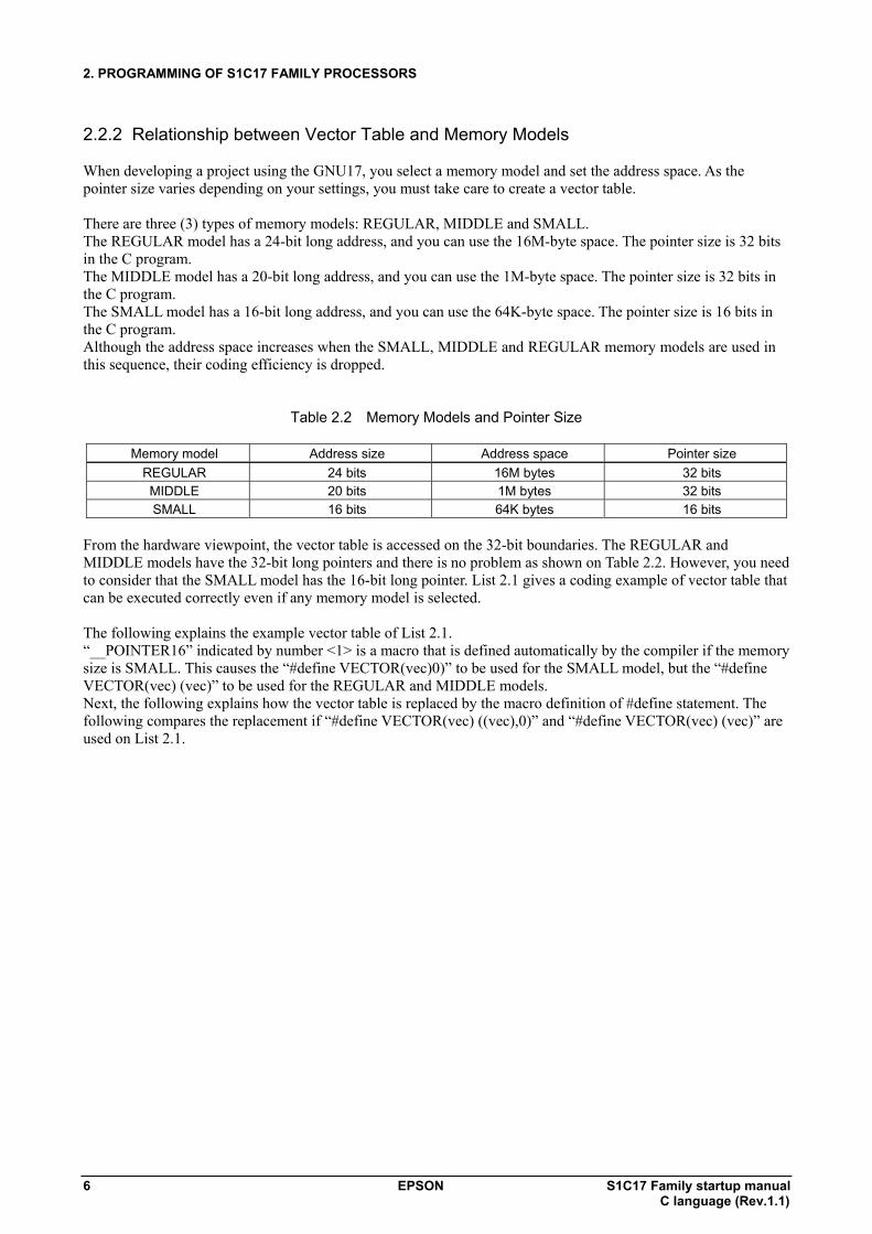
2.2.2 Relationship between Vector Table and Memory Models
When developing a project using the GNU17, you select a memory model and set the address space. As the pointer size varies depending on your settings, you must take care to create a vector table. There are three (3) types of memory models: REGULAR, MIDDLE and SMALL. The REGULAR model has a 24-bit long address, and you can use the 16M-byte space. The pointer size is 32 bits in the C program. The MIDDLE model has a 20-bit long address, and you can use the 1M-byte space. The pointer size is 32 bits in the C program. The SMALL model has a 16-bit long address, and you can use the 64K-byte space. The pointer size is 16 bits in the C program. Although the address space increases when the SMALL, MIDDLE and REGULAR memory models are used in this sequence, their coding efficiency is dropped.
Table 2.2 Memory Models and Pointer Size
Memory model Address size Address space Pointer size REGULAR 24 bits 16M bytes 32 bits MIDDLE 20 bits 1M bytes 32 bits SMALL 16 bits 64K bytes 16 bits
From the hardware viewpoint, the vector table is accessed on the 32-bit boundaries. The REGULAR and MIDDLE models have the 32-bit long pointers and there is no problem as shown on Table 2.2. However, you need to consider that the SMALL model has the 16-bit long pointer. List 2.1 gives a coding example of vector table that can be executed correctly even if any memory model is selected.
The following explains the example vector table of List 2.1. “__POINTER16” indicated by number <1> is a macro that is defined automatically by the compiler if the memory size is SMALL. This causes the “#define VECTOR(vec)0)” to be used for the SMALL model, but the “#define VECTOR(vec) (vec)” to be used for the REGULAR and MIDDLE models. Next, the following explains how the vector table is replaced by the macro definition of #define statement. The following compares the replacement if “#define VECTOR(vec) ((vec),0)” and “#define VECTOR(vec) (vec)” are used on List 2.1.

2. PROGRAMMING OF S1C17 FAMILY PROCESSORS
S1C17 Family startup manual EPSON 7 C language (Rev.1.1)
List 2.2 After Replacement of “#define VECTOR(vec)”
The example on List 2.2 has been corrected so that each item of the vector table has 32 bits long. The 16-bit area after the 16-bit pointer is set to 0s and the 32-bit length is set. The pointer is defined in the first half because the S1C17 Series CPU is accessed in the Little Endian format.
List 2.3 After Replacement of “#define VECTOR(vec) vec” On List 2.3, the vector table is configured since the pointer is 32 bits long.
/* vector table */
func *const vector[] = { // No Base+
(boot), // 0 00
(dummy), // 1 04
(nmi), // 2 08
(dummy), // 3 0c
(dummy), // 4 10
・ ・ ・
・ ・ ・
・ ・ ・
(dummy), // 30 78
(dummy) // 31 7c
}
/* vector table */
func *const vector[] = { // No Base+
((boot),0), // 0 00
((dummy),0), // 1 04
((nmi),0), // 2 08
((dummy),0), // 3 0c
((dummy),0), // 4 10
・ ・ ・
・ ・ ・
・ ・ ・
((dummy),0), // 30 78
((dummy),0) // 31 7c
}
2. PROGRAMMING OF S1C17 FAMILY PROCESSORS
8 EPSON S1C17 Family startup manual C language (Rev.1.1)
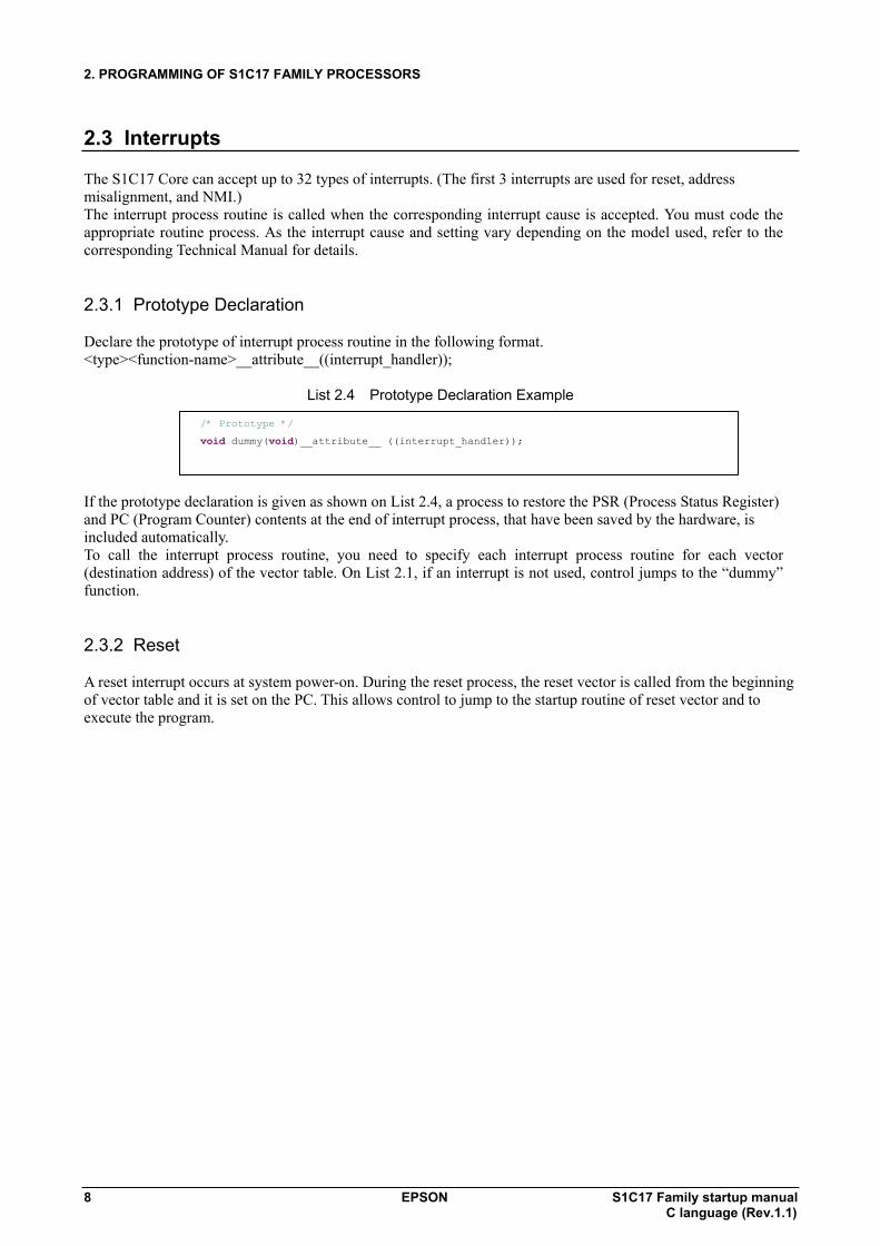
2.3 Interrupts
The S1C17 Core can accept up to 32 types of interrupts. (The first 3 interrupts are used for reset, address misalignment, and NMI.) The interrupt process routine is called when the corresponding interrupt cause is accepted. You must code the appropriate routine process. As the interrupt cause and setting vary depending on the model used, refer to the corresponding Technical Manual for details.
2.3.1 Prototype Declaration
Declare the prototype of interrupt process routine in the following format. <type><function-name>__attribute__((interrupt_handler));
List 2.4 Prototype Declaration Example
If the prototype declaration is given as shown on List 2.4, a process to restore the PSR (Process Status Register) and PC (Program Counter) contents at the end of interrupt process, that have been saved by the hardware, is included automatically. To call the interrupt process routine, you need to specify each interrupt process routine for each vector (destination address) of the vector table. On List 2.1, if an interrupt is not used, control jumps to the “dummy” function.
2.3.2 Reset
A reset interrupt occurs at system power-on. During the reset process, the reset vector is called from the beginning of vector table and it is set on the PC. This allows control to jump to the startup routine of reset vector and to execute the program.
/* Prototype */
void dummy(void)__attribute__ ((interrupt_handler));

2. PROGRAMMING OF S1C17 FAMILY PROCESSORS
S1C17 Family startup manual EPSON 9 C language (Rev.1.1)
2.3.3 Address Misalignment
A load instruction to access to memory or I/O area has the fixed size of data to be transferred by the instruction. Its address must be on a boundary of each data size.
Table 2.3 Load Instructions and Address Boundaries
Instruction Transfer data size Address
ld.b / ld.ub Bytes (8 bits) Byte boundaries (for all addresses) ld 16 bits 16-bit boundaries (The least significant bit of address is 0.) ld.a 32 bits 32-bit boundaries (The low-order 2 bits of address are 00.)
If the specified address of the load instruction does not meet these conditions, the processor considers an address misaligned interrupt and transitions to the interrupt process. On List 2.1, if an address misaligned interrupt occurs, control jumps to the “dummy” function and starts the indefinite loop process. Correct it appropriately.
2.3.4 NMI
There are two types of interrupts: maskable interrupts and non-maskable interrupts. A non-maskable interrupt is shorted as NMI. The CPU accepts this NMI unconditionally in preference to other interrupts. On List 2.1, if an NMI occurs, control jumps to the “nmi” function and the system is restored automatically. Correct it appropriately.

2. PROGRAMMING OF S1C17 FAMILY PROCESSORS
10 EPSON S1C17 Family startup manual C language (Rev.1.1)
2.4 Creating a Startup Routine
List 2.5 An Example of Startup Routine
/* #include */
#include <string.h>
/* Prototype */
void boot(void); void clearBss(void); void copyLmaToVma(void);
/* extern */
extern int main(void); extern unsigned char __START_bss; extern unsigned char __END_bss; extern unsigned char __START_data; extern unsigned char __START_data_lma; extern unsigned char __END_data;
/* Boot function */
void boot(void) { asm("xld.a %sp, 0x0fc0"); // Set SP in RAM
clearBss(); // clear the bss area
copyLmaToVma(); // copy LMA data to VMA data
asm("ei"); // interrupt enable
main(); // Call main
}
/* ClearBss function */
void clearBss(void) { memset(&__START_bss, 0, (size_t) (&__END_bss - &__START_bss));
}
/* copyLmaToVma function */
void copyLmaToVma(void) { memcpy(&__START_data, &__START_data_lma, (size_t) (&__END_data - &__START_data));
}

2. PROGRAMMING OF S1C17 FAMILY PROCESSORS
S1C17 Family startup manual EPSON 11 C language (Rev.1.1)
2.4.1 Explanation of Startup Routine
The startup routine specifies that a reset interrupt occurs during system power-on (at initial reset) and that the function is called from the vector table that corresponds to the interrupt.
Fig.2.1 Operation Flow of Startup Routine
Hardware operations
Turn the Power ON. (Initial Reset)
Generate a Reset interrupt.
Jump to the Startup routine.
Software operations
Startup routine
Set the SP.
Initialize the .data section.
Initialize the .bss section.
Enable an interrupt. (IE)
To “main” function
Call the “main” function.
2. PROGRAMMING OF S1C17 FAMILY PROCESSORS
12 EPSON S1C17 Family startup manual C language (Rev.1.1)
2.4.2 Setting the SP
First, set the start address of the stack in the SP (Stack Pointer) by issuing the “ld” instruction of the assembler.
List 2.6 SP Setup Example
Although address “0x0fc0” is set on List 2.6, you can set an address of any RAM area. Take care not to overlap the stack area by the RAM data storage area. The following explains the SP setting by considering that address 0x0fc0 is set on List 2.6. The S1C17 Series CPU places the stacks in the smaller address direction. As the S1C17701 has the RAM area of 0x0000 to 0x1000, the maximum value you can set for the SP is 0x1000. However, the 0x0fc0 to 0x0fff area is reserved for on-chip debugging. Therefore, address 0x0fc0 is set to avoid the area overlapping. Note: For the address of RAM area and on-chip debugger area, refer to the corresponding Technical Manual.
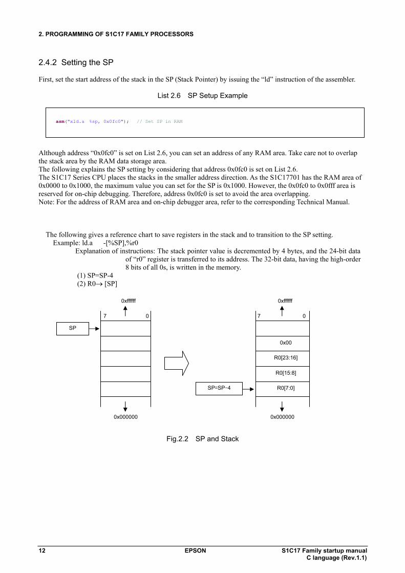
The following gives a reference chart to save registers in the stack and to transition to the SP setting. Example: ld.a -[%SP],%r0
Explanation of instructions: The stack pointer value is decremented by 4 bytes, and the 24-bit data of “r0” register is transferred to its address. The 32-bit data, having the high-order 8 bits of all 0s, is written in the memory.
(1) SP=SP-4 (2) R0→ [SP]
Fig.2.2 SP and Stack
SP
7 0
0xffffff
0x000000
SP=SP-4
0x00
R0[15:8]
R0[23:16]
R0[7:0]
7 0
0xffffff
0x000000
asm("xld.a %sp, 0x0fc0"); // Set SP in RAM
2. PROGRAMMING OF S1C17 FAMILY PROCESSORS
S1C17 Family startup manual EPSON 13 C language (Rev.1.1)
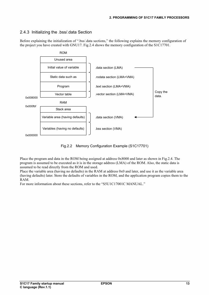
2.4.3 Initializing the .bss/.data Section Before explaining the initialization of “.bss/.data sections,” the following explains the memory configuration of the project you have created with GNU17. Fig.2.4 shows the memory configuration of the S1C17701.
Fig.2.2 Memory Configuration Example (S1C17701)
Place the program and data in the ROM being assigned at address 0x8000 and later as shown in Fig.2.4. The program is assumed to be executed as it is in the storage address (LMA) of the ROM. Also, the static data is assumed to be read directly from the ROM and used. Place the variable area (having no defaults) in the RAM at address 0x0 and later, and use it as the variable area (having defaults) later. Store the defaults of variables in the ROM, and the application program copies them to the RAM. For more information about these sections, refer to the “S5U1C17001C MANUAL.”
Copy the data.
.data section (LMA)
.rodata section (LMA=VMA)
.text section (LMA=VMA)
.vector section (LMA=VMA)
.data section (VMA)
.bss section (VMA)
Vector table
Program
Static data such as
Unused area
Initial value of variable
ROM
Stack area
Variable area (having defaults)
Variables (having no defaults)
RAM 0x008000
0x000fbf
0x000000
2. PROGRAMMING OF S1C17 FAMILY PROCESSORS
14 EPSON S1C17 Family startup manual C language (Rev.1.1)
The following explains how to initialize the .bss section. The “.bss section” stores variables having no defaults. The area from “__START_bss” to “__END_bss” is set to all 0s, and its data is cleared.
List 2.7 Initializing the .bss Section
The sample program of List 2.7 uses the “memset” function and clears the data by setting the area between
“START_bss” and “END_bss” to zero (0).
The “START_bss” and “END_bss” of external reference are defined in the “Linker script file (file.lds). ” __START_bss ....... The start address of .bss section __END_bss ....... The end address of .bss section
Note: When using the “memset” function, include the “string.h” file.
List 2.8 Initializing the .data Section
The sample program of List 2.8 uses the “memcpy” function and copies data of “START_data_lma” to the area
between “START_data” and “END_data” in the ROM (VMA). The “START_data” “START_data_lma” and “_END_data” of external reference are defined in the “Linker
script file (file.lds). ” __START_data ....... The start address of .data section __START_data_lma ....... The start address of .data section LMA part __END_data ....... The end address of .data section Note: When using the “memcpy” function, include the “string.h” file.
/* #include */
#include <string.h>
/* extern */
extern unsigned char __START_bss; extern unsigned char __END_bss;
/* ClearBss function */
void clearBss (void) { memset(&__START_bss, 0 , (size_t)(&__END_bss - &__START_bss)); }
/* #include */
#include <string.h>
/* extern */
extern unsigned char __START_data; extern unsigned char __START_data_lma; extern unsigned char __END_data;
/* copyLmaToVma function */
void copyLmaToVma(void) { memcpy(&__START_data, &__START_data_lma, (size_t) (&__END_data - &__START_data));
}

2. PROGRAMMING OF S1C17 FAMILY PROCESSORS
S1C17 Family startup manual EPSON 15 C language (Rev.1.1)
2.4.4 Enabling an Interrupt (IE)
The IE (Interrupt Enable) bit of the PSR (Processor Status Register) is set to 1 by the “ei” instruction of the assembler, and an external maskable interrupt is enabled.
List 2.9 Enabling an Interrupt (IE)
PSR is an 8-bit register that holds the CPU status data, and its content varies depending on the executed instruction result. Except for the IE bit state, you cannot directly change the content of this PSR using the program.
IL: Interrupt level (0 to 7: Interrupt) IE: Interrupt enabled (1: Enabled; 0: Disabled) C: Carry flag (1: With carry/borrow; 0: None) V: Overflow flag (1: Overflowed; 0: None) Z: Zero flag (1: Zero, 0: None-zero) N: Negative flag (1: Negative; 0: Positive)
Fig.2.3 PSR
This is a reference information only. To disable an external maskable interrupt, use the “di” instruction of the assembler as shown on List 2.10.
List 2.10 Disabling an Interrupt
asm("ei"); // interrupt enable
asm("di"); // interrupt disable
0 0 0 0 0 0 0 0
7 6 5 4 3 2 1 0
IE C V NZIL [2:0] PSR Default
3. “volatile” QUALIFIER
16 EPSON S1C17 Family startup manual C language (Rev.1.1)
3. “volatile” QUALIFIER
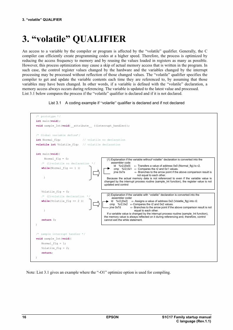
An access to a variable by the compiler or program is affected by the “volatile” qualifier. Generally, the C compiler can efficiently create programming codes at a higher speed. Therefore, the process is optimized by reducing the access frequency to memory and by reusing the values loaded in registers as many as possible. However, this process optimization may cause a skip of actual memory access that is written in the program. In such case, the control register values changed by the hardware and the variables changed by the interrupt processing may be processed without reflection of those changed values. The “volatile” qualifier specifies the compiler to get and update the variable contents each time they are referenced to, by assuming that those variables may have been changed. In other words, if a variable is defined with the “volatile” declaration, a memory access always occurs during referencing. The variable is updated to the latest value and processed. List 3.1 below compares the process if the “volatile” qualifier is declared and if it is not declared.
List 3.1 A coding example if “volarile” qualifier is declared and if not declared
Note: List 3.1 gives an example where the “-O1” optimize option is used for compiling.
/* prototype */ int main(void); void sample_Int(void)__attribute__ ((interrupt_handler)); /* Global variable define*/ int Normal_flg; // volatile no declaration
volatile int Volatile_flg; // volatile declaration
int main(void){ Normal_flg = 0;
/* (1)volatile no declaration */
while(Normal_flg == 1 ){
}
Volatile_flg = 0;
/* (2)volatile declaration */
while(Volatile_flg == 2 ){
}
return 0; }
/* sample interrupt handler */
void sample_Int(void){ Normal_flg = 1;
Volatile_flg = 2;
return; }
(1) Explanation if the variable without“volatile” declaration is converted into the assembler code
ld %r2,[0x0] ← Transfers a value of address 0x0 (Normal_flg) to r2. cmp %r2,0x1 ← Compares the r2 and 0x1 values. jrne 0x7e ← Branches to the arrow point if the above comparison result is
not equal to each other. Because the actual memory data is not referenced to even if the variable value is
changed by the interrupt process routine (sample_Int function), the register value is not updated and control
(2) Explanation if the variable with “volatile” declaration is converted into the assembler coder ld %r2,[0x2] ← Assigns a value of address 0x2 (Volatile_flg) into r2.
cmp %r2,0x2 ←Compares the r2 and 0x2 values. jrne 0x7d ← Branches to the arrow point if the above comparison result is not
equal to each other. If a variable value is changed by the interrupt process routine (sample_Int function),
the memory value is always reflected on it during referencing and, therefore, control cannot exit the while statement.
4. HOW TO ACCESS TO I/O REGISTERS
S1C17 Family startup manual EPSON 17 C language (Rev.1.1)
4. HOW TO ACCESS TO I/O REGISTERS
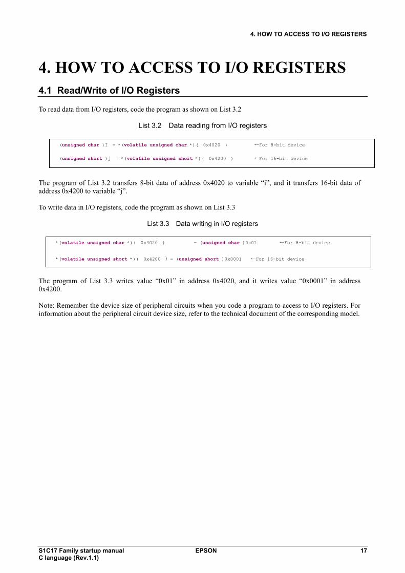
4.1 Read/Write of I/O Registers
To read data from I/O registers, code the program as shown on List 3.2
List 3.2 Data reading from I/O registers
The program of List 3.2 transfers 8-bit data of address 0x4020 to variable “i”, and it transfers 16-bit data of address 0x4200 to variable “j”.
To write data in I/O registers, code the program as shown on List 3.3
List 3.3 Data writing in I/O registers
The program of List 3.3 writes value “0x01” in address 0x4020, and it writes value “0x0001” in address 0x4200.
Note: Remember the device size of peripheral circuits when you code a program to access to I/O registers. For information about the peripheral circuit device size, refer to the technical document of the corresponding model.
(unsigned char )I = *(volatile unsigned char *)( 0x4020 ) ←For 8-bit device
(unsigned short )j = *(volatile unsigned short *)( 0x4200 ) ←For 16-bit device
*(volatile unsigned char *)( 0x4020 ) = (unsigned char )0x01 ←For 8-bit device
*(volatile unsigned short *)( 0x4200 )= (unsigned short )0x0001 ←For 16-bit device

4. HOW TO ACCESS TO I/O REGISTERS
18 EPSON S1C17 Family startup manual C language (Rev.1.1)
4.2 Bit Fields
A bit field can also be used for I/O registers. List 3.4 gives a sample coding that uses the bit field for I/O registers (having device size 8). Bit 0 of address 0x4020 is set to logical 1 on List 3.4.
List 3.4 A sample coding to use the bit field
Remember that if you use the bit field to access to an I/O register, the register is accessed in unit of bytes. For details, refer to the “Data the detailed information, refer to the “Data representation” section of the “Compile Output” in the “S5U1C17001C Manual. ”
Do not try to write data in I/O registers using the bit field if a register is reset if a register bit is set to logical 1. If you use such I/O registers, access to them in the method as described in Section 4.1. List 3.5 gives a sample coding which uses the bit field and writes data in an I/O register if the register is reset when a register bit is set to logical 1.
List 3.5 A coding example
The sample coding of List 3.5 resets all logical-1 bits to zero (0) although you wish to reset only bit 0 of address 0x4020.
/* If address 0x4020 (the I/O register which is reset to 0 if register bit is set to logical 1) is 0xaa */ xld.a %r3,0x4020 ld.b %r2,[%r3] ← r2 value (01010101) or %r2,0x1 ← r2 value (01010101) ld.b [%r3],%r2 ← r3 value (01010101)⇒ r3 value (00000000)
/* Bit Field For Byte Data. */
struct BbitF { unsigned int b0 : 1;
unsigned int b1 : 1;
unsigned int b2 : 1;
unsigned int b3 : 1;
unsigned int b4 : 1;
unsigned int b5 : 1;
unsigned int b6 : 1;
unsigned int b7 : 1;
};
/* Sample Register */
#define BF_SAMPLE (*(volatile struct BbitF *)( 0x4020))
/* Sample Register writing */
BF_SAMPLE.b0 = 1;
Explanation after data conversion into assembler code xld.a %r3,0x4020 Transfers value 0x4020 to r3. ld.b %r2,[%r3] ← Transfers value of r3 (address 0x4020) to r2. or %r2,0x1 ← Transfers value r2 exclusively ORed with 0x1 (bit
0) to r2. ld.b [%r3],%r2 ←Transfers value of r3 (address 0x4020) to r2.

REVISION HISTORY
S1C17 Family startup manual EPSON 19 C language (Rev.1.1)
REVISION HISTORY
Date revision modification note 08/08/18 1.0 First edition 08/09/18 1.1 Cover correction

International Sales Operations
AMERICA EPSON ELECTRONICS AMERICA, INC. HEADQUARTERS 2580 Orchard Parkway San Jose , CA 95131,USA Phone: +1-800-228-3964 FAX: +1-408-922-0238 SALES OFFICES Northeast 301 Edgewater Place, Suite 210 Wakefield, MA 01880, U.S.A. Phone: +1-800-922-7667 FAX: +1-781-246-5443 EUROPE EPSON EUROPE ELECTRONICS GmbH HEADQUARTERS Riesstrasse 15 Muenchen Bayern, 80992 GERMANY Phone: +49-89-14005-0 FAX: +49-89-14005-110
ASIA EPSON (CHINA) CO., LTD. 7F, Jinbao Bldg.,No.89 Jinbao St., Dongcheng District, Beijing 100005, China Phone: +86-10-6410-6655 FAX: +86-10-6410-7320 SHANGHAI BRANCH 7F, Block B, Hi-Tech Bldg., 900, Yishan Road, Shanghai 200233, CHINA Phone: +86-21-5423-5522 FAX: +86-21-5423-5512 EPSON HONG KONG LTD. 20/F., Harbour Centre, 25 Harbour Road Wanchai, Hong Kong Phone: +852-2585-4600 FAX: +852-2827-4346 Telex: 65542 EPSCO HX EPSON (CHINA) CO., LTD. SHENZHEN BRANCH 12/F, Dawning Mansion, Keji South 12th Road, Hi- Tech Park, Shenzhen Phone: +86-755-2699-3828 FAX: +86-755-2699-3838 EPSON TAIWAN TECHNOLOGY & TRADING LTD. 14F, No. 7, Song Ren Road, Taipei 110 Phone: +886-2-8786-6688 FAX: +886-2-8786-6660 EPSON SINGAPORE PTE., LTD. 1 HarbourFront Place, #03-02 HarbourFront Tower One, Singapore 098633 Phone: +65-6586-5500 FAX: +65-6271-3182 SEIKO EPSON CORPORATION KOREA OFFICE 50F, KLI 63 Bldg., 60 Yoido-dong Youngdeungpo-Ku, Seoul, 150-763, KOREA Phone: +82-2-784-6027 FAX: +82-2-767-3677 GUMI OFFICE 2F, Grand B/D, 457-4 Songjeong-dong, Gumi-City, KOREA Phone: +82-54-454-6027 FAX: +82-54-454-6093 SEIKO EPSON CORPORATION SEMICONDUCTOR OPERATIONS DIVISION IC Sales Dept. IC International Sales Group 421-8, Hino, Hino-shi, Tokyo 191-8501, JAPAN Phone: +81-42-587-5814 FAX: +81-42-587-5117

Document code: 411551201
First issue August, 2008 in JAPAN
Revised September 2008 in JAPAN
EPSON Electronic Devices Website
SEIKO EPSON CORPORATION
http://www.epson.jp/device/semicon_e/
S1C17 Family Startup Manual C language
SEMICONDUCTOR OPERATIONS DIVISION