CMB Detectors, multiplexing, readout – survey of current ...
36
CMB Detectors, multiplexing, readout – survey of current technologies and prospects for CMB-S4 August 26, 2016 DRAFT CMB-S4 Collaboration
Transcript of CMB Detectors, multiplexing, readout – survey of current ...
CMB Detectors, multiplexing, readout – survey of currenttechnologies and prospects for CMB-S4
August 26, 2016
DRAFT
CMB-S4 Collaboration
Contents1 Goal of CMB-S4 instrument technology survey papers 1
2 Introduction 2
3 Transition Edge Sensors 33.1 Description . . . . . . . . . . . . . . . . . . . . . . . . . . . . . . . . . . . . . . 33.2 Performance . . . . . . . . . . . . . . . . . . . . . . . . . . . . . . . . . . . . . . 33.3 Prospects and R&D path for CMB-S4 . . . . . . . . . . . . . . . . . . . . . . . . 4
4 Microwave Kinetic Inductance Detectors (MKIDs) 64.1 Description of the Technology . . . . . . . . . . . . . . . . . . . . . . . . . . . . 64.2 Demonstrated Performance . . . . . . . . . . . . . . . . . . . . . . . . . . . . . . 64.3 Prospects, Scaling for CMB-S4 . . . . . . . . . . . . . . . . . . . . . . . . . . . . 7
5 Time Domain Multiplexing 95.1 Technical description . . . . . . . . . . . . . . . . . . . . . . . . . . . . . . . . . 95.2 Demonstrated Performance . . . . . . . . . . . . . . . . . . . . . . . . . . . . . . 115.3 Prospects and R&D path towards CMB-S4 . . . . . . . . . . . . . . . . . . . . . . 11
6 Frequency Domain Multiplexing 136.1 Technical description . . . . . . . . . . . . . . . . . . . . . . . . . . . . . . . . . 136.2 Demonstrated Performance . . . . . . . . . . . . . . . . . . . . . . . . . . . . . . 14
6.2.1 Achieved MUX factors . . . . . . . . . . . . . . . . . . . . . . . . . . . . 146.2.2 Thermal loading and power consumption . . . . . . . . . . . . . . . . . . 156.2.3 Noise . . . . . . . . . . . . . . . . . . . . . . . . . . . . . . . . . . . . . 156.2.4 Crosstalk . . . . . . . . . . . . . . . . . . . . . . . . . . . . . . . . . . . 15
6.3 Prospects and R&D path for CMB-S4 . . . . . . . . . . . . . . . . . . . . . . . . 16
7 Microwave SQUIDs 177.1 Technical description . . . . . . . . . . . . . . . . . . . . . . . . . . . . . . . . . 177.2 Demonstrated Performance . . . . . . . . . . . . . . . . . . . . . . . . . . . . . . 177.3 Prospects and R&D path for CMB-S4 . . . . . . . . . . . . . . . . . . . . . . . . 18
8 Microwave Multiplexing for MKIDs 208.1 Description of the Technology . . . . . . . . . . . . . . . . . . . . . . . . . . . . 208.2 Demonstrated Performance . . . . . . . . . . . . . . . . . . . . . . . . . . . . . . 218.3 Prospects, Scaling for CMB-S4 . . . . . . . . . . . . . . . . . . . . . . . . . . . . 21
i

1 Goal of CMB-S4 instrument technology survey papersSummarize the current state of the technology and identify R&D efforts necessary to advanceit for possible use in CMB-S4. CMB-S4 will likely require a scale-up in number of elements,frequency coverage, and bandwidth relative to current instruments. Because it is searching forlower magnitude signals, it will also require stronger control of systematic uncertainties.
1

2 Introduction
2
3 Transition Edge Sensors
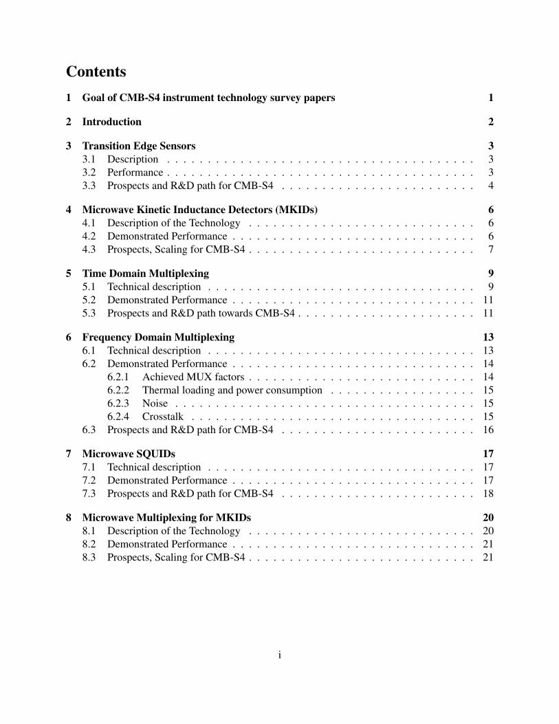
3.1 DescriptionA Transition Edge Sensor (TES) is a highly sensitive thermometer consisting of a thin supercon-ducting film weakly heat-sunk to a bath temperature much lower than the superconductor Tc (seeFig. 1, left). By supplying a voltage bias to the TES, the sensor can operate in the middle of itssuperconducting-to-normal transition where small changes to the TES temperature, arising fromthermal fluctuations (noise) or changes in the absorbed power from a source (signal), lead to largechanges in the TES electrical resistance. Due to the shape of the TES transition, the applied voltagebias establishes a negative feedback loop [?] where the change in TES resistance cancels externalchanges in absorbed power. This negative electro-thermal feedback is very strong because thetransition is very sharp linearizing the detector response and expanding the detector bandwidth.
The theoretical foundations of TES dynamics are well developed [?] providing good descrip-tions of the noise and response for real devices. The irreducible noise for a TES detector arisesfrom phonon fluctuations in the TES weak thermal link. For CMB applications, this thermal fluc-tuation noise is comparable or subdominant to the photon “shot noise” for TES with Tc in the rangeof 100-500 mK. Thus, TES bolometers can achieve nearly “background limited” sensitivities.
The voltage-biased TES is a low impedance device that is well matched to readouts usingDC Superconducting QUantum Interference Devices (SQUIDs). SQUIDs have a large noise mar-gin over the detector noise enabling multiplexed detector readout schemes (see TDM, FDM anduMUX). Multiplexed readout is important for operating large arrays of detectors at sub-Kelvintemperatures.
3.2 PerformanceTES detectors have been applied across a diverse set of CMB experimental platforms. Currentdetector architectures utilize low-loss superconducting microstrip coupled to planar structures torealize optical bandpass definition, polarization analysis, beam synthesis and radiation coupling(see RF coupling paper). Examples of implemented TES architectures include the phased antennaarray fabricated at JPL and used by the SPIDER, BICEP2, BICEP3 and Keck Array experiments,lenslet coupled antennas used by the Polarbear experiment, absorber coupled devices used by theEBEX and SPTpol (90 GHz) experiments, and feedhorn coupled devices with planar orthomodetransducers used by the ABS, CLASS, ACTpol and SPTpol (150 GHz) experiments. For thesedetector architectures, the RF performance can be modeled and simulated with results in goodagreement with measured performance. TES detectors have been successfully used across 40 GHz-300 GHz, the entire optical frequency range envisioned for CMB-S4, with detectors achievingnoise equivalent powers of 30-50 aW/rtHz (nearly background limited). Detectors deployed at lowoptical frequencies (∼40 GHz) and ballon-borne payloads have demonstrated even lower noiseequivalent powers of ∼10 aW/rtHz. In multiple deployed experiments, the TES noise is consistentwith what is predicted from theoretical modeling and the ensemble of deployed experiments haverealized background limited performance across all relevant angular scales.
3
Heat Sink (~240 mK)
Weak thermal link, G-‐1
Heat Capacity
Psignal TES
T+δT
δT
δR
Figure 1: Left: Illustration of a thermal circuit for a typical Transition Edge Sensor (TES) detectorhighlighting the principles of signal detection. A weakly thermally sunk heat capacity absorbspower, Psignal, which is to be measured. Variations in the absorbed power change the heat capac-ity’s temperature, which is measured by a TES operating under strong electro-thermal feedback.Right: Plot of resistance versus temperature for a typical TES illustrating the principles of negativeelectro-thermal feedback [?]. The TES is voltage biased into the middle of its superconducting-to-normal transition. Small changes in the TES temperature produce large changes in the TESresistance. Since the TES is voltage biased, an increase (or decrease) in the temperature producesan increase (or decrease) in the resistance leading to a decrease (or increase) in the Joule heatingpower supplied by the bias. This canceling effect corresponds to a strong negative electro-thermalfeedback making the current through the TES nearly proportional to Psignal.
3.3 Prospects and R&D path for CMB-S4Given the maturity, diversity and demonstrated performance of TES-based CMB detectors, theTES bolometer technology is at a high technical readiness level where risks associated with de-tector design and implementation are low. The R&D focus for using TES detectors in CMB-S4 ison scaled production. TES detectors are fabricated via micro-machining of thin films deposited onsilicon wafer substrates. However, unlike semiconductor-based detectors, the absence of a devel-oped superconducting integrated circuit industry means commercial production options having therequisite economies of scale are not readily available.
• Increased Production Throughput Current TES detector array fabrication typically in-volves processing ∼10 layers of materials with fabrication times of 3-6 weeks for fabricat-ing 5-10 arrays. Modest and low risk improvements to fabrication techniques and logistics(e.g. interleaved fabrication batches) are expected to increase this throughput. The primaryrequirement for increasing TES production is access to micro-fabrication resources with ex-clusive control of the thin film deposition systems. This exclusive access to microfabricationtooling can be addressed with national lab resources.
• Improved Production Reliability The primary challenge for scaling TES detector arraysfor CMB-S4 is improving the fabrication consistency. Addressing this challenge requires
4
a short term R&D program focused on understanding the connection between variations infabrication processing and superconducting RF circuit performance and mechanical ther-mal properties. Improving production reliability also requires establishing test facilities andorganizing a quality assurance program among the universities and national labs.
• Multiplexed TES Readout Multiplexed TES readouts are required for implementing focalplanes with more than 1000 detector elements and will continue to be an active componentfor R&D. Modest improvements over existing fielded multiplexer technology should be suf-ficient. However, recent developments with microwave-based readout techniques for TESdetectors may lead to new multiplexer technologies with broader applicability and lowercost, and could be synergistic with mKID readout development efforts.
5
4 Microwave Kinetic Inductance Detectors (MKIDs)
4.1 Description of the TechnologyMicrowave kinetic inductance detectors (MKIDs) are superconducting thin-film, GHz resonatorsthat are designed to also be optimal photon absorbers [1]. Absorbed photons with energies greaterthan the superconducting gap (ν > 2∆/h ∼= 74 GHz×(Tc/1 K)) break Cooper pairs, changing thedensity of quasiparticles in the device. The quasiparticle density affects the kinetic inductance andthe dissipation of the superconducting film, so a changing optical signal will cause the resonantfrequency and internal quality factor of the resonator to shift. These changes in the properties ofthe resonator can be detected as changes in the amplitude and phase of a probe tone that drivesthe resonator at its resonant frequency. This detector technology is particularly well-suited forsub-kelvin, kilo-pixel detector arrays because each detector element can be dimensioned to havea unique resonant frequency, and the probe tones for hundreds to thousands of detectors can becarried into and out of the cryostat on a single pair of coaxial cables (see Section 8).
The total instrument noise is the quadrature sum of the detector noise and the photon noise,and the fundamental performance goal is to achieve a sensitivity that is dominated by the ran-dom arrival of background photons. For an MKID, the detector noise includes contributions fromthree sources: generation-recombination (g-r) noise, two-level system (TLS) noise, and ampli-fier noise [1]. The g-r noise comes from the random recombination of quasiparticles. At typicaloperating temperatures and optical loads, quasiparticle generation noise is dominated by opticalgeneration – the photon noise – and thermal generation is negligible. TLS noise is produced bydielectric fluctuations due to quantum two level systems in amorphous dielectric surface layerssurrounding the MKID. The scaling of TLS noise with operating temperature, resonator geometry,and readout tone power and frequency has been extensively studied experimentally and is welldescribed by a semi-empirical model [2]. Finally, the amplifier noise is the electronic noise of thereadout system, which is dominated by the cryogenic microwave low-noise amplifier.
4.2 Demonstrated PerformanceA range of MKID-based instruments have already shown that MKIDs work at millimeter andsub-millimeter wavelengths. Early MKIDs used antenna coupling [3], and these antenna-coupledMKIDs were demonstrated at the Caltech Submillimeter Observatory (CSO) in 2007 [4] leadingto the development of MUSIC, a multi-chroic antenna-coupled MKID camera [5]. A simpler de-vice design that uses the inductor in a single-layer LC resonator to directly absorb the millimeterand sub-millimeter-wave radiation was published in 2008 [6]. This style of MKID, called thelumped-element kinetic inductance detector (LEKID), was first demonstrated in 2011 in the 224-pixel NIKA dual-band millimeter-wave camera on the 30 m IRAM telescope in Spain [7]. Photonnoise limited horn-coupled LEKIDs sensitive to 1.2 THz were recently demonstrated [8] and thesedetectors will be used in the balloon-borne experiment BLAST-TNG [9, 10]. A large format sub-millimeter wavelength camera, called A-MKID, with more than 20,000 pixels and a readout multi-plexing factor greater than 1,000 has been built and is currently being commissioned at the APEXtelescope in the Atacama Desert in Chile [11]. Laboratory studies have shown that state-of-the-art
6
polarization 1
polarization 2
capa
citiv
ely
coup
led
bias
sig
nal horn exit
aperture
cylindricalwaveguide
conicalor proled
horn
4.8 mm aperture
160 μm Si
inductors choke
IDC IDCbias
aluminumdetectorpackage
IDC
IDC
inductors
backshort prototype module (20 horns)
lterattachment
probe tones in
horn array
probe tones out to LNA
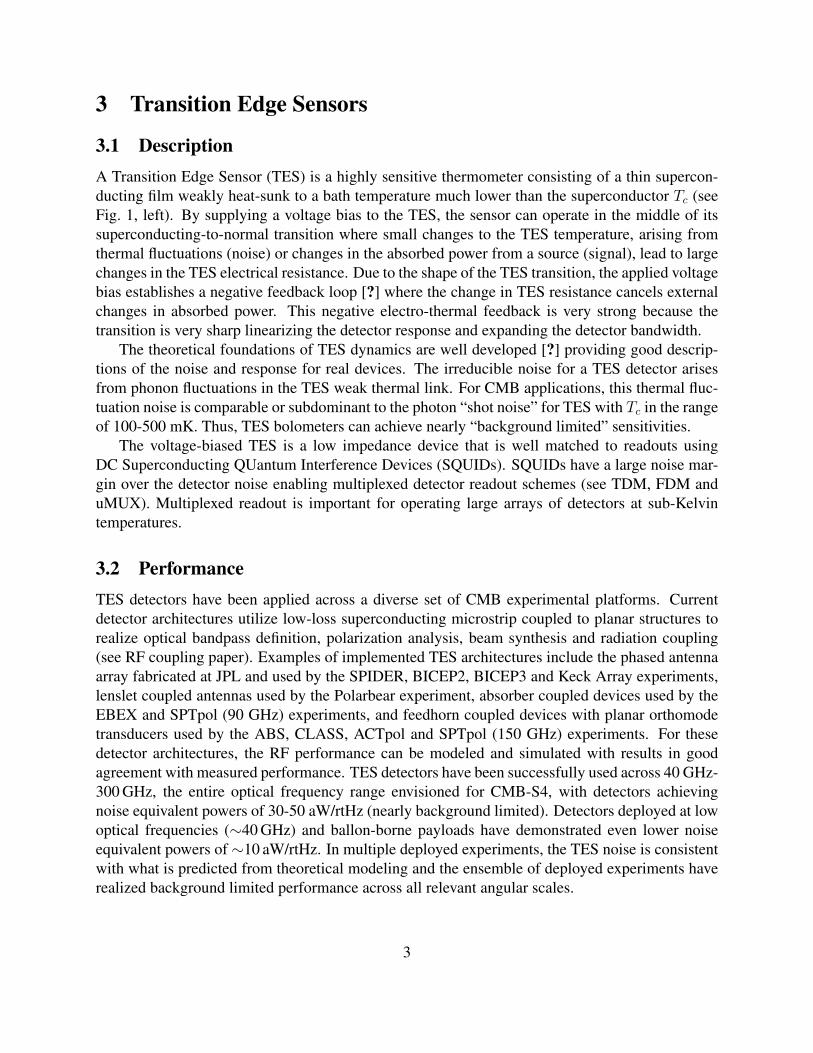
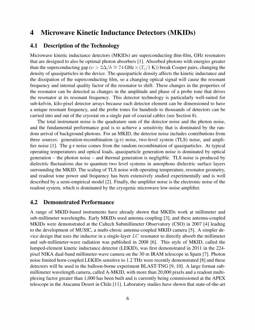
Figure 2: Left: Schematic of a dual-polarization lumped-element kinetic inductance detector(LEKID) that is sensitive to one spectral band centered on 150 GHz [18]. The LC resonatorsensitive to the horizontal polarization is colored red, while the resonator sensitive to the orthogonalpolarization is colored blue. The inductor in the resonator is the photon absorber. The dotted circlerepresents the waveguide exit aperture at the back of the horn. The resonators are driven by a probetone capactively coupled to a transmission line for read out, which is colored green. Center: Across-sectional view of a single array element. The LEKIDs are fabricated on silicon and directlyilluminated. The horn aperture tapers to a cylindrical waveguide which also acts as a high-passfilter. A choke matches the impedance between the waveguide and the LEKID absorber, whilealso controlling lateral radiation loss along the array inside the detector module. The aluminumbottom of the module acts as the backshort, and the backshort distance is set by the silicon waferthickness. Right: A photograph of a 20-element dual-polarization LEKID module.
MKID and LEKID designs can achieve photon noise limited performance [12, 13, 14, 15]. Andfinally, on-chip spectrometers based on MKIDs are currently being developed [16, 17].
4.3 Prospects, Scaling for CMB-S4Two scalable varieties of MKID – using two completely different RF coupling strategies – are cur-rently being developed for CMB polarization studies with CMB-S4 in mind: (i) dual-polarizationlumped-element kinetic inductance detectors (LEKIDs), which are shown in Figure 2 and (ii) horn-coupled, multi-chroic MKIDs, which are shown in Figure 3 [20, 18]. The details of the RF cou-pling designs are discussed in Section ??. The horn-coupled, multi-chroic devices are based onthe polarimeters that were developed for the Advanced ACTPol experiment [21, 22], though inthe new MKID-based version, the TES bolometers are replaced with hybrid co-planar waveguide(CPW) MKIDs, and the millimeter-wave circuit is fully re-optimized for silicon-on-insulator (SOI)wafers. The multi-chroic MKIDs are still in the development stage, and a laboratory performancedemonstration will be completed in late 2016 or early 2017. The noise-equivalent temperature(NET), noise-equivalent power (NEP), in-band spectral response, pulse response (time constant),
7
hybridCPWMKID
slotline
aluminumsection
niobiumsection
microstrip from
λ/4 CPW resonator probe tones
niobiumground plane
hybridtee
band-passlters
OMT
microstrip-to-CPW coupler
hybrid tee
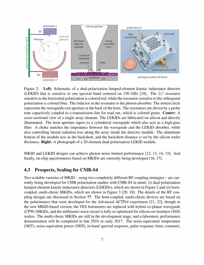
Figure 3: Left: One polarization sensitive multi-chroic MKID array element. Each array elementis sensitive to two polarizations and two polarizations, so there are four MKIDs per element. Right:A schematic of the microstrip-to-CPW coupling schematic. The millimeter-wave power is coupledfrom the microstrip output of the hybrid tee to the CPW of the MKID using a novel, broadbandcircuit [19].
low-frequency noise performance, and multiplexing performance of LEKIDs have all been studiedextensively in the laboratory [18, 12, 13]. These studies have revealed that the performance ofLEKIDs can be compared with that of state-of-the-art TES bolometers – especially for ground-based experiments when the optical loading is greater than approximately 1 pW. Arrays with ap-proximately 500 single-polarization detectors are currently being built. An on-sky demonstrationis the critical next step for LEKIDs.
It is possible to make the sensing element in the MKIDs out of aluminum manganese instead ofaluminum. By adding manganese to the aluminum, the Tc of the sensor decreases in a controllableway [23], which does two critical things. First and foremost, at 120 GHz and above, the photonsare energetic enough to break multiple Cooper pairs in the sensing element, so the detector noisewill be further suppressed below the photon noise – even for the low optical loads that are expectedin a space-like environment. Second, a lower Tc makes the detector technology sensitive to lowerfrequencies (∼30 GHz), so one AlMn MKID architecture could be used for all of the spectral bandsin CMB-S4.
8
5 Time Domain Multiplexing
5.1 Technical descriptionIn time-division multiplexing (TDM), a column of detectors is combined by addressing each de-tector one at a time in a sequence. We focus primarily on the system architecture developed atNIST [24, 25] and readout electronics developed at UBC [26] as applied to the readout of largearrays of transition-edge sensors (TESs).
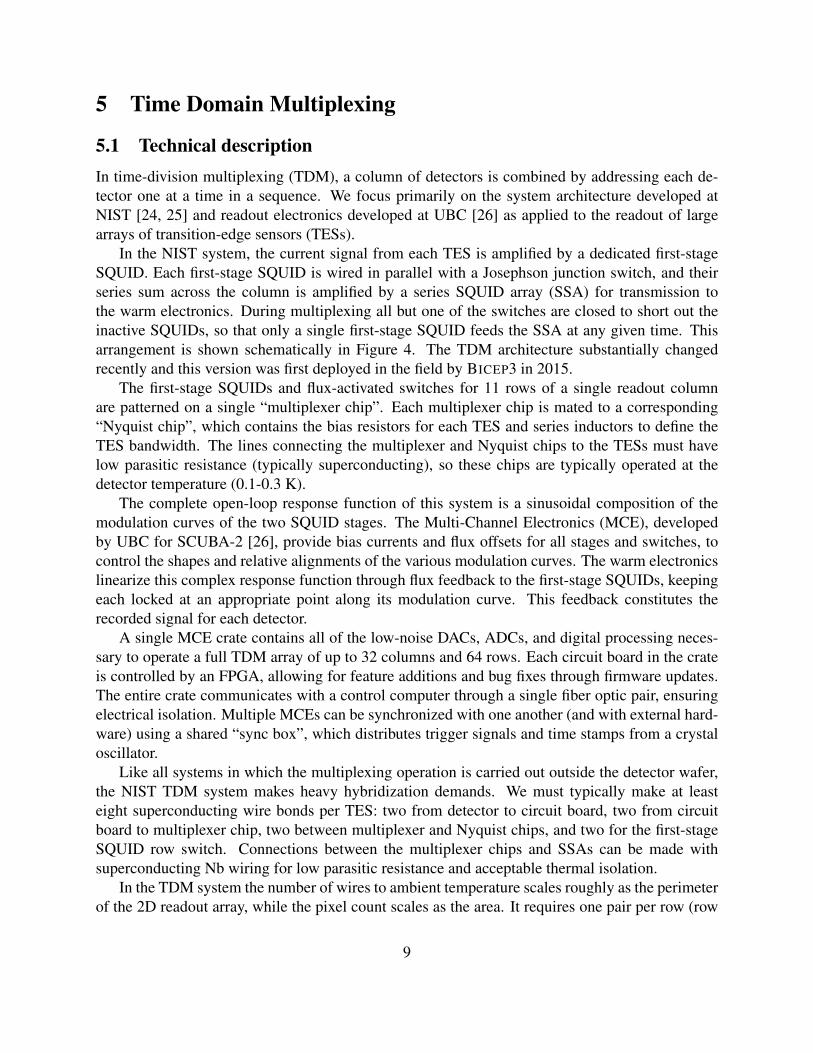
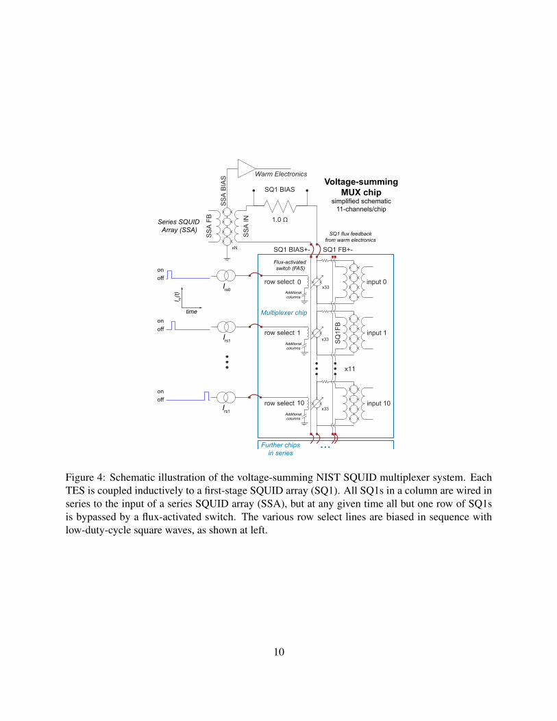
In the NIST system, the current signal from each TES is amplified by a dedicated first-stageSQUID. Each first-stage SQUID is wired in parallel with a Josephson junction switch, and theirseries sum across the column is amplified by a series SQUID array (SSA) for transmission tothe warm electronics. During multiplexing all but one of the switches are closed to short out theinactive SQUIDs, so that only a single first-stage SQUID feeds the SSA at any given time. Thisarrangement is shown schematically in Figure 4. The TDM architecture substantially changedrecently and this version was first deployed in the field by BICEP3 in 2015.
The first-stage SQUIDs and flux-activated switches for 11 rows of a single readout columnare patterned on a single “multiplexer chip”. Each multiplexer chip is mated to a corresponding“Nyquist chip”, which contains the bias resistors for each TES and series inductors to define theTES bandwidth. The lines connecting the multiplexer and Nyquist chips to the TESs must havelow parasitic resistance (typically superconducting), so these chips are typically operated at thedetector temperature (0.1-0.3 K).
The complete open-loop response function of this system is a sinusoidal composition of themodulation curves of the two SQUID stages. The Multi-Channel Electronics (MCE), developedby UBC for SCUBA-2 [26], provide bias currents and flux offsets for all stages and switches, tocontrol the shapes and relative alignments of the various modulation curves. The warm electronicslinearize this complex response function through flux feedback to the first-stage SQUIDs, keepingeach locked at an appropriate point along its modulation curve. This feedback constitutes therecorded signal for each detector.
A single MCE crate contains all of the low-noise DACs, ADCs, and digital processing neces-sary to operate a full TDM array of up to 32 columns and 64 rows. Each circuit board in the crateis controlled by an FPGA, allowing for feature additions and bug fixes through firmware updates.The entire crate communicates with a control computer through a single fiber optic pair, ensuringelectrical isolation. Multiple MCEs can be synchronized with one another (and with external hard-ware) using a shared “sync box”, which distributes trigger signals and time stamps from a crystaloscillator.
Like all systems in which the multiplexing operation is carried out outside the detector wafer,the NIST TDM system makes heavy hybridization demands. We must typically make at leasteight superconducting wire bonds per TES: two from detector to circuit board, two from circuitboard to multiplexer chip, two between multiplexer and Nyquist chips, and two for the first-stageSQUID row switch. Connections between the multiplexer chips and SSAs can be made withsuperconducting Nb wiring for low parasitic resistance and acceptable thermal isolation.
In the TDM system the number of wires to ambient temperature scales roughly as the perimeterof the 2D readout array, while the pixel count scales as the area. It requires one pair per row (row
9
SQ
1FB
SS
A F
B
SS
A IN
SS
A B
IAS
x33
x33
x33
xN
1.0 Ω
SQ1 FB+-SQ1 BIAS+-
Series SQUID Array (SSA)
Warm Electronics
Multiplexer chip
Voltage-summingMUX chip
simplified schematic11-channels/chip
SQ1 flux feedbackfrom warm electronics
Flux-activated switch (FAS)
Further chipsin series
...
Additionalcolumns
Additionalcolumns
Additionalcolumns
Irs0
ono
time
I rs(t)
Irs1
ono
Irs1
ono
Figure 4: Schematic illustration of the voltage-summing NIST SQUID multiplexer system. EachTES is coupled inductively to a first-stage SQUID array (SQ1). All SQ1s in a column are wired inseries to the input of a series SQUID array (SSA), but at any given time all but one row of SQ1sis bypassed by a flux-activated switch. The various row select lines are biased in sequence withlow-duty-cycle square waves, as shown at left.
10

select) and four pair per column (bias and feedback for the first-stage SQUIDs and SSA). Theseconnections are typically twisted pairs with few-MHz bandwidth.
5.2 Demonstrated PerformanceThis architecture is now very mature and has extensive field heritage on a variety of CMB instru-ments, including ABS [27], ACT [28], ACTpol [29], BICEP2 [30], BICEP3 [31], CLASS [32],Keck Array [33], and SPIDER [34].
The achievable multiplexing factor is constrained by the ratio of readout bandwidth to TESbandwidth. TES bandwidth is generally bounded below at several kHz by considerations of stabil-ity [35], so higher multiplexing factors require higher readout bandwidth. Readout bandwidth istypically set by the SQUID amplifier and interconnects, notably by the L/R time constant of thefirst-stage SQUIDs driving the SSA input coil, and the RC time constant of the cables to ambienttemperature. Advanced ACTpol is currently deploying the highest achieved multiplexing factor of64 TES channels per readout column using the NIST TDM chips and the UBC electronics [36].
Since the readout chain’s bandwidth must be much higher than the sampling rate of any givenTES, noise from the SQUIDs and warm amplifiers is heavily aliased. The aliasing penalty forr.m.s. noise is proportional to the square root of the multiplexing factor, but there is some freedomto limit the aliasing impact by reducing detector resistance or adding turns to the SQUID input coil.In practice the impact from the SQUID/amplifier alone is negligible. If the detector bandwidth isnot sufficiently below the multiplexing rate, the detector noise can be aliased as well: BICEP2with a 25 kHz TDM revisit frequency experienced∼14% aliased noise penalty to its total (photon-noise-dominated) NET [37]
Current instruments dissipate ∼1.8 nW per readout column at the detector temperature (100-300 mK) [38, 39]. This should not scale strongly with multiplexing factor, since it is dominated bythe single first-stage SQUID that is operational at any given time.
The series SQUID arrays dissipate substantially more power: ∼1 µW per readout column. Thispower may be dissipated at a somewhat higher temperature (typically 1–4 K), and so is typicallynot a limiting factor.
TDM has several known crosstalk mechanisms, generally of modest amplitude [25, 30]. Thelargest form of crosstalk is inductive: each first-stage SQUID detects current from neighboringinput coils (adjacent rows in the same readout column) inductively at the ∼0.3 % level, and at ayet smaller level to more distant rows. In a well designed system, all other forms of crosstalk aresubdominant.
A typical full-sized (72-HP) MCE crate serving a ∼2000 pixel (32 column by 64 row) arrayconsumes 85 watts, supplied by custom linear or switched DC supplies. The crate dimensions areapproximately 40 × 43 × 34 cm (depth / width / height) and weighs approximately 13 kg, notincluding separate DC supplies.
5.3 Prospects and R&D path towards CMB-S4For CMB-S4, the large number of detectors per telescope require a higher multiplexing factor.Starting from the Advanced ACTpol 64-way multiplexer, careful tuning of TES and SQUID prop-
11
erties could potentially double readout bandwidth while halving TES bandwidth, for a total multi-plexing factor of order ∼200. Larger factors seem difficult to reconcile with current interconnectbandwidth and TES stability concerns. Such a multiplexing system would currently, for each32-column (6400 TES) readout array, incorporate more than 70,000 Josephson junctions at basetemperature, involve more than 50,000 wire bonds, require ∼264 wire pairs to base temperature,and dissipate ∼32 nW at base temperature per array.
The TDM system brings several advantages to CMB-S4, including heritage and demonstratedmultiplexing factor. The TDM system has almost a decade of field experience on science instru-ments, leading to dozens of publications involving a total of more than 10,000 detectors. Thehardware and software are well-characterized and well-supported. Systematics are controlled andwell-understood for multiplexing factors of 64.
The challenges for this technology include a relatively large cryocable count and heavy hy-bridization costs. Since row-switching in TDM is carried out at ambient temperature, wires toroom temperature are required for each row as well as each column. That leads to a relativelyhigh wire count per pixel: roughly 8 pairs to sub-Kelvin per readout column for a 32×200 array.Like other technologies where multiplexing is separated from the detector wafer, the hybridiza-tion requirements are substantial: at least eight bonds per TES, plus four per readout column. Anadvantage to this system, however, is that the cables are relatively simple twisted-pair cryogeniccables, as much as 3 m long.
12
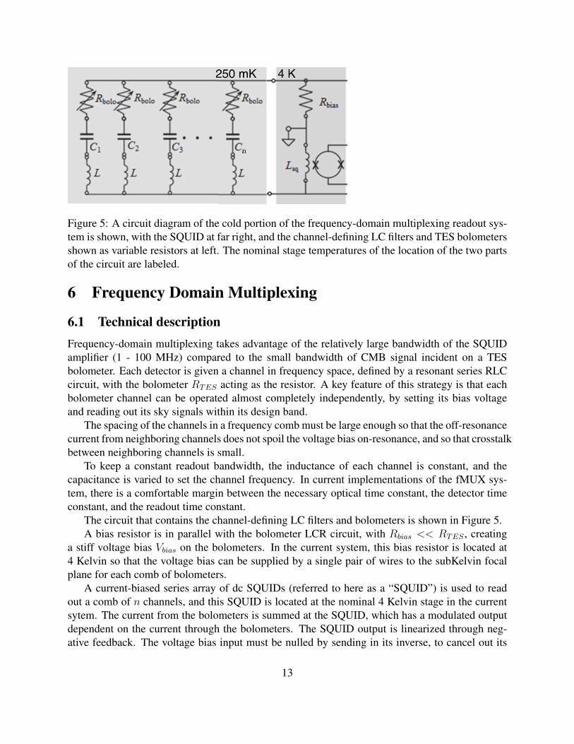
Figure 5: A circuit diagram of the cold portion of the frequency-domain multiplexing readout sys-tem is shown, with the SQUID at far right, and the channel-defining LC filters and TES bolometersshown as variable resistors at left. The nominal stage temperatures of the location of the two partsof the circuit are labeled.
6 Frequency Domain Multiplexing
6.1 Technical descriptionFrequency-domain multiplexing takes advantage of the relatively large bandwidth of the SQUIDamplifier (1 - 100 MHz) compared to the small bandwidth of CMB signal incident on a TESbolometer. Each detector is given a channel in frequency space, defined by a resonant series RLCcircuit, with the bolometer RTES acting as the resistor. A key feature of this strategy is that eachbolometer channel can be operated almost completely independently, by setting its bias voltageand reading out its sky signals within its design band.
The spacing of the channels in a frequency comb must be large enough so that the off-resonancecurrent from neighboring channels does not spoil the voltage bias on-resonance, and so that crosstalkbetween neighboring channels is small.
To keep a constant readout bandwidth, the inductance of each channel is constant, and thecapacitance is varied to set the channel frequency. In current implementations of the fMUX sys-tem, there is a comfortable margin between the necessary optical time constant, the detector timeconstant, and the readout time constant.
The circuit that contains the channel-defining LC filters and bolometers is shown in Figure 5.A bias resistor is in parallel with the bolometer LCR circuit, with Rbias << RTES , creating
a stiff voltage bias Vbias on the bolometers. In the current system, this bias resistor is located at4 Kelvin so that the voltage bias can be supplied by a single pair of wires to the subKelvin focalplane for each comb of bolometers.
A current-biased series array of dc SQUIDs (referred to here as a “SQUID”) is used to readout a comb of n channels, and this SQUID is located at the nominal 4 Kelvin stage in the currentsytem. The current from the bolometers is summed at the SQUID, which has a modulated outputdependent on the current through the bolometers. The SQUID output is linearized through neg-ative feedback. The voltage bias input must be nulled by sending in its inverse, to cancel out its
13

contribution to current through the SQUID. In the present implementation, the sky signal is alsonulled, so that the SQUID acts as an error sensor, and the nulling current is the sky signal.
The operation of the resonant RLC circuit depends on there being negligible impedance inseries with the well-defined components of the circuit. The bolometer resistance RTES must bethe dominant resistance, and there also must be minimal stray inductance from wiring and cir-cuit boards. These components and wiring are all at sub-Kelvin temperatures, which helps toachieve these specifications. The wiring from the SQUID and bias resistor at 4 Kelvin to the sub-Kelvin focal plane must be low inductance while acting as a thermal break, which is achieved withbroadside-coupled NbTi striplines. The practical lengths and inductances of the current sub-Kelvinwiring and components requires RTES ≈ 1Ω, to keep the bolometer impedance large compared toother impedances.
The fMUX readout system uses custom warm electronics designed at McGill University [40],[41], [42]. These synthesize the bolometer voltage biases (labeled “Carrier Bias Comb”), thenulling signal that is applied to the SQUID to increase its dynamic range (labeled “Nulling Comb”),and the demodulators. The SQUID has a transimpedance that is high enough to convert smallcurrent through the bolometers into a voltage that is read out with a room-temperature amplifier.
6.2 Demonstrated Performance6.2.1 Achieved MUX factors
Stage-2 CMB polarization experiments have demonstrated frequency-domain multiplexing factorsof 8× - 16×, including POLARBEAR-1, [43, 44], SPT-Pol[45, 46], and EBEX[47].
Stage-2 fMux systems used shunt-feedback to linearize the SQUID response, which providednegative feedback over the entire bandwidth. This limited the SQUID bandwidth to ∼ 1.3 MHz,due to the difficulty maintaining stability across a large bandwidth. The channels were definedwith commercial surface mount capacitors, which limited the accuracy of channel placement andthe quality factor of the resonant circuit. This resulted in a practical limit of about 16× for themultiplexing factor[47].
To extend the usable bandwidth, the feedback was changed to a form of baseband feedbackknown as Digital Active Nulling (DAN) [41], where feedback is applied only around the bolome-ter carrier frequencies. Using DAN instead of shunt feedback, channels can be placed anywhere inthe SQUID bandwidth, which for the series arrays presently used is 50-100 MHz. Using DANfeedback also removes any constraints on wiring length between the cold SQUID and room-temperature amplifier. DAN feedback has been demonstrated on the sky with the SPT-Pol ex-periment, and will be used for all fMux systems in the future.
To improve the precision of channel placement and to reduce loss at higher frequencies, su-perconducting resonator components were developed at UC Berkeley and Lawrence Berkeley Na-tional Laboratory [48, 49]. An interdigitated capacitor pattern is used along with a spiral inductorpattern, in order to simplify the design to a single layer of superconducting traces. These compo-nents are patterned onto single-crystal silicon, with one chip for each multiplexed comb.
These developments greatly increased the potential multiplexing factor for the fMUX systemused in Stage-3 experiments, deploying around the end of 2016. POLARBEAR-2 will have a
14

multiplexing factor of 40[50], and SPT-3G will have a multiplexing factor of 68[51].
6.2.2 Thermal loading and power consumption
In the current implementation of the fMux system, there is no power dissipation at the subKelvinstages from readout components. There is only one pair of wires running to the subKelvin stagesfor each multiplexed comb of bolometers. This wiring must be low impedance, while also servingas a thermal break, and currently broadside-coupled NbTi striplines are used for this. The thermalload on the focal plane from these wires is about ∼ 1nW per comb. There is also minimal powerdissipated at the other temperature stages from readout wiring, relative to other contributions andthe cooling capacity. The readout system dissipates power at the 4 Kelvin stage in the currentsystem, from SQUIDs and bias resistors,<≈ 1µW per comb.
The power and space requirements for the warm electronics are relatively small. The roomtemperature readout electronics can operate 8000 detector channels per 9U crate, with 1 kW ofpower draw.
6.2.3 Noise
For the fMUX system, the design requirements are based on limiting each fundamental readoutnoise source to contribute less than 15% of the minimum expected noise equivalent current causedby the bolometer power noise terms. The limiting factors are the noise performance of roomtemperature components, including the first stage amplifier for the SQUID output and the DAC thatgenerates the carrier voltages. This results in a design NEIreadout expectation of ∼ 7 pA/
√Hz.
For POLARBEAR-1, the measured NEIreadout was slightly higher, ∼ 9 pA/√
Hz.
6.2.4 Crosstalk
In the fMUX system, signal crosstalk onto a detector can only occur if the crosstalk signal lieswithin its frequency bandwidth. Other crosstalk can still be a problem since it can introduce excessloading on the SQUID, or create noise problems, but does not introduce false sky signals. Sincethe fraction of total SQUID bandwith that is occupied by detector signals is very small, there is asmall amount of crosstalk from its nearest neighbors in frequency space and physical space in thecomb. There is also the possibility of crosstalk from another comb if there is a source of crosstalkand the detector’s frequency bands overlap. The physical layout of pixels and LC channels andthe layout of channels into combs and frequency channels can be arranged so that no detectors areneighbors or share a pixel in both physical space and frequency space. POLARBEAR-1 had thehighest level of signal crosstalk from neighbors in frequency space, with a maximum level of about1%[44].
• 1/f knee
• Bandwidth, Stability
15
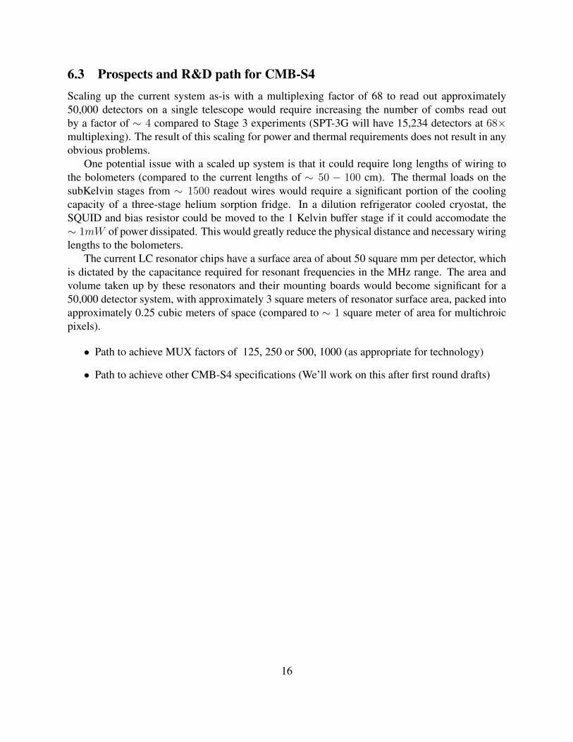
6.3 Prospects and R&D path for CMB-S4Scaling up the current system as-is with a multiplexing factor of 68 to read out approximately50,000 detectors on a single telescope would require increasing the number of combs read outby a factor of ∼ 4 compared to Stage 3 experiments (SPT-3G will have 15,234 detectors at 68×multiplexing). The result of this scaling for power and thermal requirements does not result in anyobvious problems.
One potential issue with a scaled up system is that it could require long lengths of wiring tothe bolometers (compared to the current lengths of ∼ 50 − 100 cm). The thermal loads on thesubKelvin stages from ∼ 1500 readout wires would require a significant portion of the coolingcapacity of a three-stage helium sorption fridge. In a dilution refrigerator cooled cryostat, theSQUID and bias resistor could be moved to the 1 Kelvin buffer stage if it could accomodate the∼ 1mW of power dissipated. This would greatly reduce the physical distance and necessary wiringlengths to the bolometers.
The current LC resonator chips have a surface area of about 50 square mm per detector, whichis dictated by the capacitance required for resonant frequencies in the MHz range. The area andvolume taken up by these resonators and their mounting boards would become significant for a50,000 detector system, with approximately 3 square meters of resonator surface area, packed intoapproximately 0.25 cubic meters of space (compared to ∼ 1 square meter of area for multichroicpixels).
• Path to achieve MUX factors of 125, 250 or 500, 1000 (as appropriate for technology)
• Path to achieve other CMB-S4 specifications (We’ll work on this after first round drafts)
16
7 Microwave SQUIDs
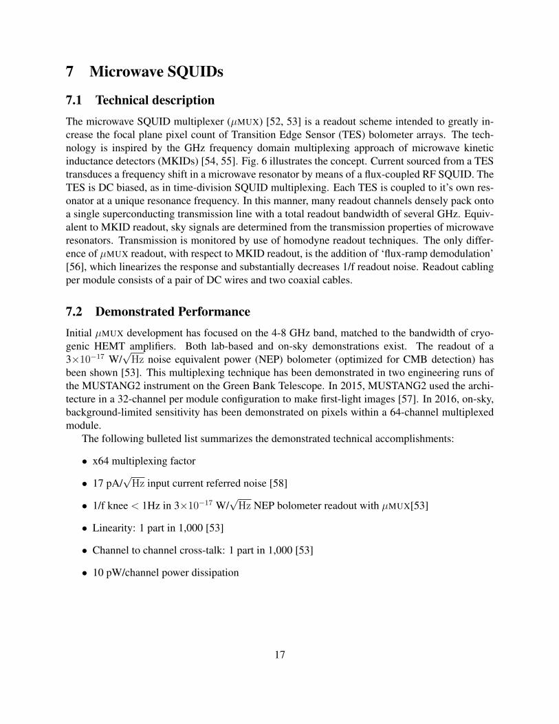
7.1 Technical descriptionThe microwave SQUID multiplexer (µMUX) [52, 53] is a readout scheme intended to greatly in-crease the focal plane pixel count of Transition Edge Sensor (TES) bolometer arrays. The tech-nology is inspired by the GHz frequency domain multiplexing approach of microwave kineticinductance detectors (MKIDs) [54, 55]. Fig. 6 illustrates the concept. Current sourced from a TEStransduces a frequency shift in a microwave resonator by means of a flux-coupled RF SQUID. TheTES is DC biased, as in time-division SQUID multiplexing. Each TES is coupled to it’s own res-onator at a unique resonance frequency. In this manner, many readout channels densely pack ontoa single superconducting transmission line with a total readout bandwidth of several GHz. Equiv-alent to MKID readout, sky signals are determined from the transmission properties of microwaveresonators. Transmission is monitored by use of homodyne readout techniques. The only differ-ence of µMUX readout, with respect to MKID readout, is the addition of ‘flux-ramp demodulation’[56], which linearizes the response and substantially decreases 1/f readout noise. Readout cablingper module consists of a pair of DC wires and two coaxial cables.
7.2 Demonstrated PerformanceInitial µMUX development has focused on the 4-8 GHz band, matched to the bandwidth of cryo-genic HEMT amplifiers. Both lab-based and on-sky demonstrations exist. The readout of a3×10−17 W/
√Hz noise equivalent power (NEP) bolometer (optimized for CMB detection) has
been shown [53]. This multiplexing technique has been demonstrated in two engineering runs ofthe MUSTANG2 instrument on the Green Bank Telescope. In 2015, MUSTANG2 used the archi-tecture in a 32-channel per module configuration to make first-light images [57]. In 2016, on-sky,background-limited sensitivity has been demonstrated on pixels within a 64-channel multiplexedmodule.
The following bulleted list summarizes the demonstrated technical accomplishments:
• x64 multiplexing factor
• 17 pA/√
Hz input current referred noise [58]
• 1/f knee < 1Hz in 3×10⁻¹⁷ W/√
Hz NEP bolometer readout with µMUX[53]
• Linearity: 1 part in 1,000 [53]
• Channel to channel cross-talk: 1 part in 1,000 [53]
• 10 pW/channel power dissipation
17
0
♦
5.45 5.50 5.55 5.60 5.6520
15
10
5
0
Tra
nsm
issio
n (
dB
)
Frequency (GHz)
st
t①
②
s s
|S2
1|2
(dB
)
Frequency (GHz)5.454 5.456 5.458 5.46
-10
-20
st
Figure 6: Overview of the the microwave SQUID multiplexer. (a) Schematic of the circuit. (b) Photograph of a 32-channel µMUX chip. (c) S21 transmission measurement of the µMUX with 32 active channels. (d) Variation of singlereadout channel transmission curves to applied input magnetic flux (or equivalently applied current when inductivelycoupled).
7.3 Prospects and R&D path for CMB-S4The µMUX is less mature than time-division SQUID multiplexing (TDM) or MHz frequency-division SQUID multiplexing (FDM), which together have been used to readout∼30,000 deployedTES detectors that observe in the millimeter/sub-millimeter/FIR. In contrast, the µMUX has onlybeen demonstrated on one astronomical instrument with 215 pixels. Nevertheless, the µMUX maybe the most promising technique to enable the readout of TES bolometers in the quantity requiredfor CMB-S4. Already the demonstrated multiplexing factor is equal to that of TDM (x64, Ad-vanced ACTPol [59]) and upcoming FDM (x64, SPT-3G [60]) experiments. The achieved mul-tiplexing density (6 MHz resonator spacing) and available HEMT amplifier bandwidth (4 GHz)dictate that multiplexing factors of 660 are attainable. Recent developments in fabrication suggestthat the multiplexing density may be increased by more than a factor of two.
The warm electronics used in the µMUX borrows largely from MKID readout developments.Several architectures exist. MUSTANG2 uses a ROACH1 platform with firmware developed byNRAO+UPENN. NIST is developing µMUX-specific readout based on the ROACH2 platform andhas used it to demonstrate undegraded readout of a 4-pixel array of TES microcalorimeters. Stan-ford/SLAC is developing an alternative readout, which includes tone-tracking. This techniqueeases the requirements of the follow-on, wide-bandwidth amplifer. The power consumption of thewarm readout is platform specific. For reference, the power consumption of a ROACH2 board is∼45W (??).
The µMUX may be developed as a stand-alone multiplexing technique for CMB-S4, or it mayfind use in a hybrid multiplexing scheme. Hybrid multiplexing is a common way to more effi-ciently use available bandwidth. For example, it is the approach used in 3G cell phone technology.For readout of TES bolometers, a lower bandwidth multiplexing scheme, such as TDM or code-division multiplexing, is embedded within a wider bandwidth GHz resonator. Therefore each
18
GHz tone carries the signals from N bolometers, where N may be 32 or 64. A proof-of-conceptdemonstration was shown in 2008 [61]. Significant but straightforward effort will be required todemonstrate readiness for CMB-S4 for either stand-alone or hybrid multiplexing schemes.
19
8 Microwave Multiplexing for MKIDs
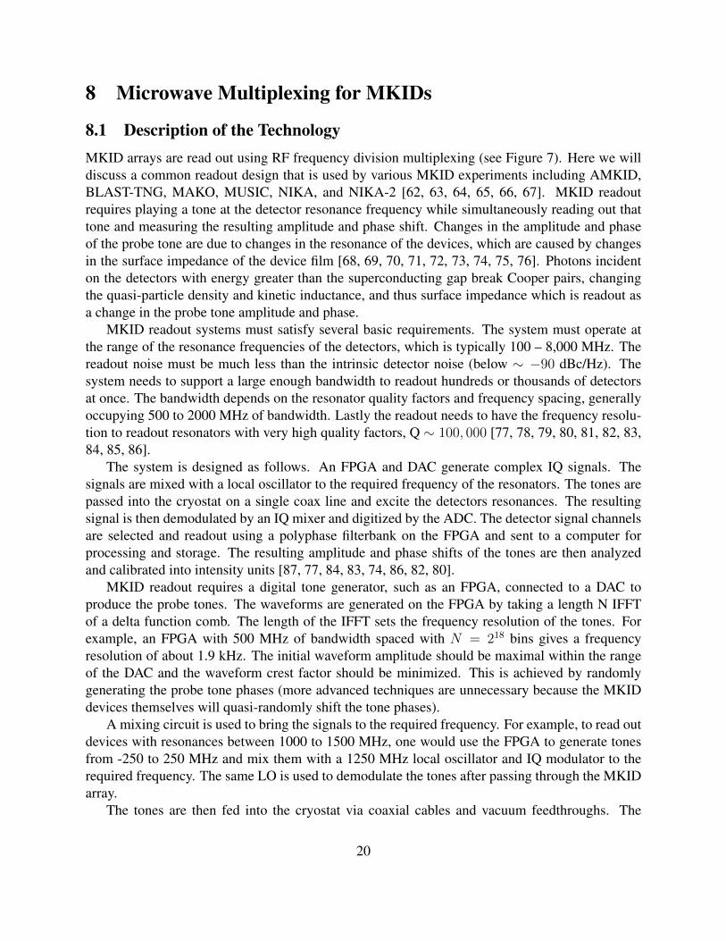
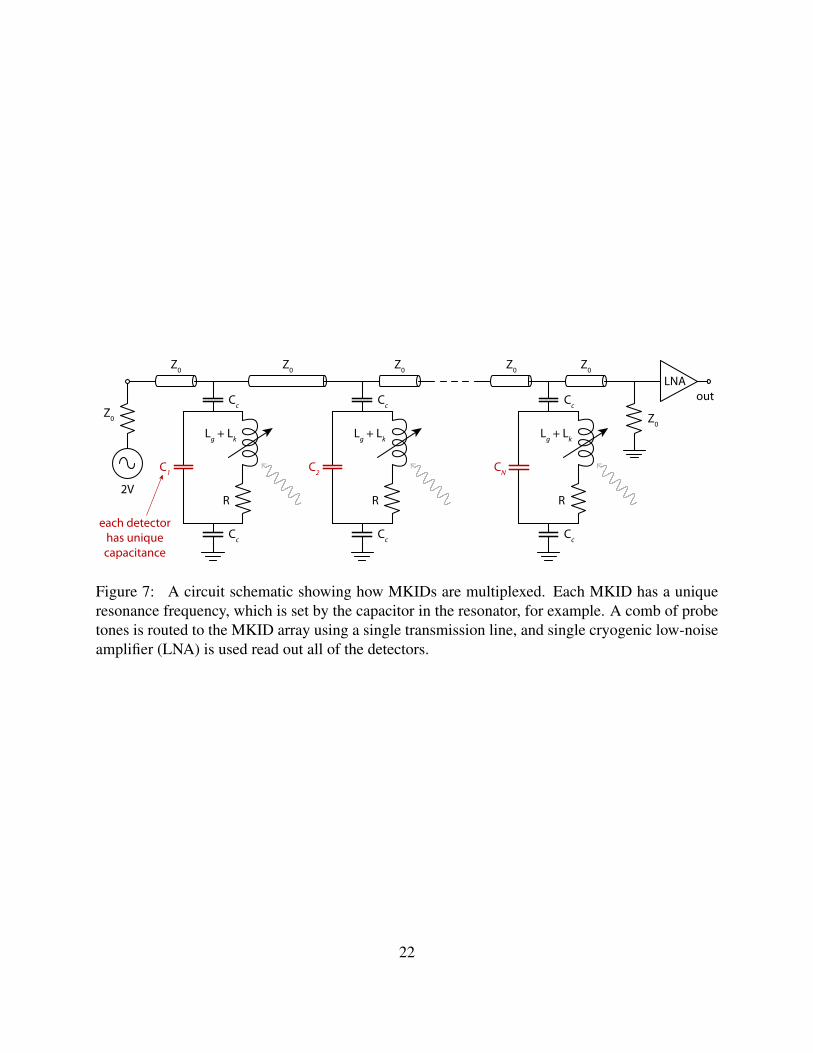
8.1 Description of the TechnologyMKID arrays are read out using RF frequency division multiplexing (see Figure 7). Here we willdiscuss a common readout design that is used by various MKID experiments including AMKID,BLAST-TNG, MAKO, MUSIC, NIKA, and NIKA-2 [62, 63, 64, 65, 66, 67]. MKID readoutrequires playing a tone at the detector resonance frequency while simultaneously reading out thattone and measuring the resulting amplitude and phase shift. Changes in the amplitude and phaseof the probe tone are due to changes in the resonance of the devices, which are caused by changesin the surface impedance of the device film [68, 69, 70, 71, 72, 73, 74, 75, 76]. Photons incidenton the detectors with energy greater than the superconducting gap break Cooper pairs, changingthe quasi-particle density and kinetic inductance, and thus surface impedance which is readout asa change in the probe tone amplitude and phase.
MKID readout systems must satisfy several basic requirements. The system must operate atthe range of the resonance frequencies of the detectors, which is typically 100 – 8,000 MHz. Thereadout noise must be much less than the intrinsic detector noise (below ∼ −90 dBc/Hz). Thesystem needs to support a large enough bandwidth to readout hundreds or thousands of detectorsat once. The bandwidth depends on the resonator quality factors and frequency spacing, generallyoccupying 500 to 2000 MHz of bandwidth. Lastly the readout needs to have the frequency resolu-tion to readout resonators with very high quality factors, Q ∼ 100, 000 [77, 78, 79, 80, 81, 82, 83,84, 85, 86].
The system is designed as follows. An FPGA and DAC generate complex IQ signals. Thesignals are mixed with a local oscillator to the required frequency of the resonators. The tones arepassed into the cryostat on a single coax line and excite the detectors resonances. The resultingsignal is then demodulated by an IQ mixer and digitized by the ADC. The detector signal channelsare selected and readout using a polyphase filterbank on the FPGA and sent to a computer forprocessing and storage. The resulting amplitude and phase shifts of the tones are then analyzedand calibrated into intensity units [87, 77, 84, 83, 74, 86, 82, 80].
MKID readout requires a digital tone generator, such as an FPGA, connected to a DAC toproduce the probe tones. The waveforms are generated on the FPGA by taking a length N IFFTof a delta function comb. The length of the IFFT sets the frequency resolution of the tones. Forexample, an FPGA with 500 MHz of bandwidth spaced with N = 218 bins gives a frequencyresolution of about 1.9 kHz. The initial waveform amplitude should be maximal within the rangeof the DAC and the waveform crest factor should be minimized. This is achieved by randomlygenerating the probe tone phases (more advanced techniques are unnecessary because the MKIDdevices themselves will quasi-randomly shift the tone phases).
A mixing circuit is used to bring the signals to the required frequency. For example, to read outdevices with resonances between 1000 to 1500 MHz, one would use the FPGA to generate tonesfrom -250 to 250 MHz and mix them with a 1250 MHz local oscillator and IQ modulator to therequired frequency. The same LO is used to demodulate the tones after passing through the MKIDarray.
The tones are then fed into the cryostat via coaxial cables and vacuum feedthroughs. The
20
coax is then wired through to the required cold stages and attenuated before interacting with thedetectors. The signal is then passed into a cold low noise amplifier and then back out of thecryostat. The signal is again amplified and mixed down before going into an ADC and back intothe digital readout. Signals are then demodulated into amplitude and phase shifts, which can becalibrated to intensity variations on the detectors.
8.2 Demonstrated PerformanceState of the art MKID readout systems can support thousands of resonators [87, 77, 82, 86, 85, 88,66, 81]. Current on sky instruments have demonstrated multiplexing factors of 400 [64, 84]. Acombination of the digital readout bandwidth and resonator quality factors determine the maximumnumber of detectors that can be readout with negligible electronic cross talk. For a typical systemwith 500 MHz of bandwidth centered on 1 GHz and resonant frequencies spaced by 10 times thewidth, the MKIDs must have a quality factor greater than 10,000 while optically loaded. In labsystems have demonstrated multiplexing factors up to 4000 while maintaining the required noiseperformance [77].
8.3 Prospects, Scaling for CMB-S4MKID readout is typically limited by the detector devices rather than the electronic readout. Cur-rent tone generation and multiplexing is capable of reading out thousands of detectors. Limitationsarise from resonance quality factors and resonant frequency collisions within the set bandwidth ofthe readout. MKID readout systems are also applicable for readout of TES bolometers [89, 90].Current readout research focuses on increasing the bandwidth and speed of the ADC/DAC cards.The total power consumption of the system is dominated by the warm electronics and totals around100W [77]. The readout heat loading in the cryostat is due only to the RF signal and LNA powerusage.
21
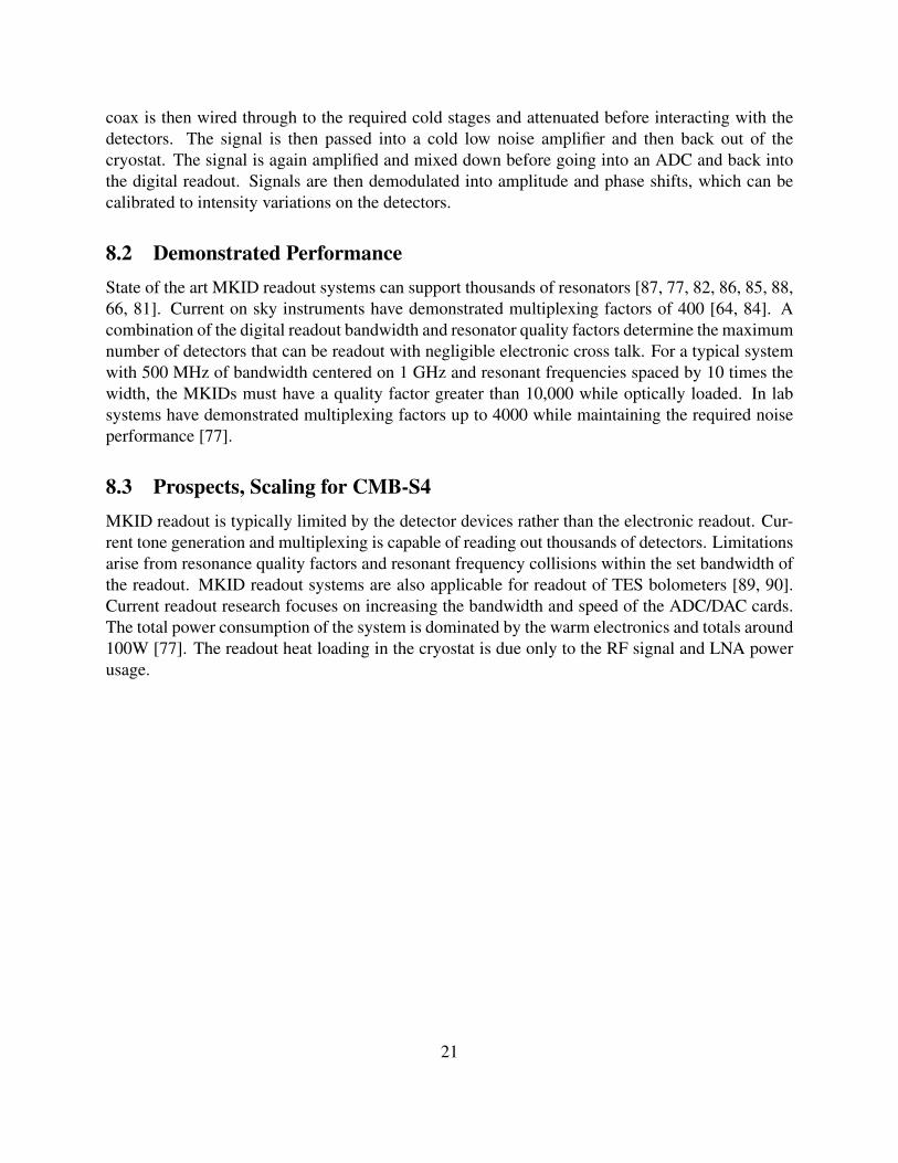
Lg + Lk
R
C1
Cc
Cc
Z0
Z0Z0
out
2V
LNA
Lg + Lk
R
C2
Cc
Cc
Z0 Z0 Z0
Lg + Lk
R
CN
Cc
Cc
Z0
each detectorhas uniquecapacitance
Figure 7: A circuit schematic showing how MKIDs are multiplexed. Each MKID has a uniqueresonance frequency, which is set by the capacitor in the resonator, for example. A comb of probetones is routed to the MKID array using a single transmission line, and single cryogenic low-noiseamplifier (LNA) is used read out all of the detectors.
22
DCblock
DCblock
DCblock
-20 dB attenuator
LNA
-20 dB attenuator
duroid
duroid
detector array
SScoax
SScoax
SScoax
SScoax
NbTicoax
CuNicoax
45 K 3.5 K 100 mK
Cryostat
SMAfeed-
through
Low-PassFilters
Low-PassFilters
DigitalAttenuator
DAC
ADC
ROACH-2Board
Amplier
lterbank
300 K
LocalOscillator
ROACH-2
ADC/DAC
10 Gbit Ethernet
attenuator
mixers
amplierLO
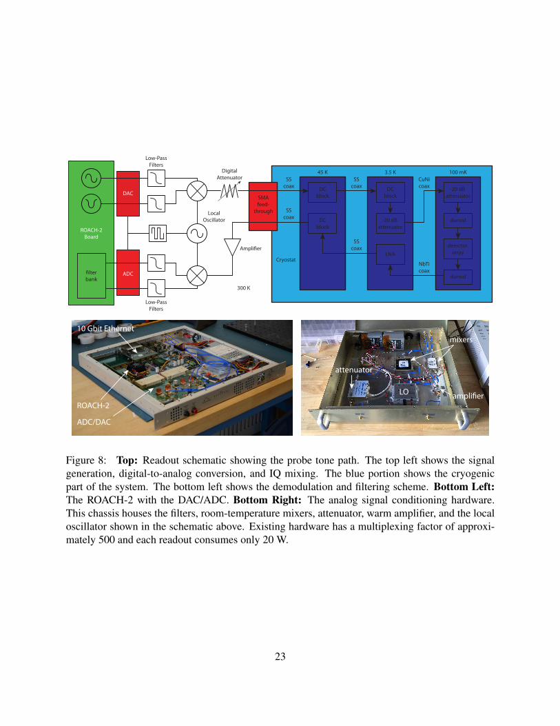
Figure 8: Top: Readout schematic showing the probe tone path. The top left shows the signalgeneration, digital-to-analog conversion, and IQ mixing. The blue portion shows the cryogenicpart of the system. The bottom left shows the demodulation and filtering scheme. Bottom Left:The ROACH-2 with the DAC/ADC. Bottom Right: The analog signal conditioning hardware.This chassis houses the filters, room-temperature mixers, attenuator, warm amplifier, and the localoscillator shown in the schematic above. Existing hardware has a multiplexing factor of approxi-mately 500 and each readout consumes only 20 W.
23
References[1] J. Zmuidzinas. Superconducting Microresonators: Physics and Applications. Ann. Rev. Cond.
Matt. Phys., 3:169–214, 2012.
[2] J. Gao, M. Daal, J. M. Martinis, A. Vayonakis, J. Zmuidzinas, B. Sadoulet, B. A. Mazin, P. K.Day, and H. G. Leduc. A semiempirical model for two-level system noise in superconductingmicroresonators. Applied Physics Letters, 92(21):212504, May 2008.
[3] P. K. Day, H. G. Leduc, A. Goldin, T. Vayonakis, B. A. Mazin, S. Kumar, J. Gao, andJ. Zmuidzinas. Antenna-coupled microwave kinetic inductance detectors. Nuclear Instru-ments and Methods in Physics Research A, 559:561–563, April 2006.
[4] J. Schlaerth, A. Vayonakis, P. Day, J. Glenn, J. Gao, S. Golwala, S. Kumar, H. Leduc,B. Mazin, J. Vaillancourt, and J. Zmuidzinas. A Millimeter and Submillimeter Kinetic In-ductance Detector Camera. Journal of Low Temperature Physics, 151:684–689, May 2008.
[5] S. R. Golwala, C. Bockstiegel, S. Brugger, N. G. Czakon, P. K. Day, T. P. Downes, R. Duan,J. Gao, A. K. Gill, J. Glenn, M. I. Hollister, H. G. LeDuc, P. R. Maloney, B. A. Mazin,S. G. McHugh, D. Miller, O. Noroozian, H. T. Nguyen, J. Sayers, J. A. Schlaerth, S. Siegel,A. K. Vayonakis, P. R. Wilson, and J. Zmuidzinas. Status of MUSIC, the MUltiwavelengthSub/millimeter Inductance Camera. In Society of Photo-Optical Instrumentation Engineers(SPIE) Conference Series, volume 8452, Sept. 2012.
[6] S. Doyle, P. Mauskopf, J. Naylon, A. Porch, and C. Duncombe. Lumped Element KineticInductance Detectors. Journal of Low Temperature Physics, 151:530–536, April 2008.
[7] A. Monfardini, A. Benoit, A. Bideaud, L. Swenson, A. Cruciani, P. Camus, C. Hoffmann,F. X. Desert, S. Doyle, P. Ade, P. Mauskopf, C. Tucker, M. Roesch, S. Leclercq, K. F.Schuster, A. Endo, A. Baryshev, J. J. A. Baselmans, L. Ferrari, S. J. C. Yates, O. Bourrion,J. Macias-Perez, C. Vescovi, M. Calvo, and C. Giordano. A Dual-band Millimeter-wave Ki-netic Inductance Camera for the IRAM 30 m Telescope. Astrophys. J. Supp., 194:24, June2011.
[8] J. Hubmayr, J. Beall, D. Becker, H.-M. Cho, M. Devlin, B. Dober, C. Groppi, G. C. Hilton,K. D. Irwin, D. Li, P. Mauskopf, D. P. Pappas, J. Van Lanen, M. R. Vissers, Y. Wang, L. F.Wei, and J. Gao. Photon-noise limited sensitivity in titanium nitride kinetic inductance de-tectors. Applied Physics Letters, 106(7):073505, February 2015.
[9] N. Galitzki, P. A. R. Ade, F. E. Angile, P. Ashton, J. A. Beall, D. Becker, K. J. Bradford,G. Che, H.-M. Cho, M. J. Devlin, B. J. Dober, L. M. Fissel, Y. Fukui, J. Gao, C. E. Groppi,S. Hillbrand, G. C. Hilton, J. Hubmayr, K. D. Irwin, J. Klein, J. van Lanen, D. Li, Z.-Y. Li,N. P. Lourie, H. Mani, P. G. Martin, P. Mauskopf, F. Nakamura, G. Novak, D. P. Pappas,E. Pascale, G. Pisano, F. P. Santos, G. Savini, D. Scott, S. Stanchfield, C. Tucker, J. N.Ullom, M. Underhill, M. R. Vissers, and D. Ward-Thompson. The Next Generation BLASTExperiment. Journal of Astronomical Instrumentation, 3:1440001, 2014.
24
[10] B. J. Dober, P. A. R. Ade, P. Ashton, F. E. Angile, J. A. Beall, D. Becker, K. J. Bradford,G. Che, H.-M. Cho, M. J. Devlin, L. M. Fissel, Y. Fukui, N. Galitzki, J. Gao, C. E. Groppi,S. Hillbrand, G. C. Hilton, J. Hubmayr, K. D. Irwin, J. Klein, J. Van Lanen, D. Li, Z.-Y. Li,N. P. Lourie, H. Mani, P. G. Martin, P. Mauskopf, F. Nakamura, G. Novak, D. P. Pappas,E. Pascale, F. P. Santos, G. Savini, D. Scott, S. Stanchfield, J. N. Ullom, M. Underhill, M. R.Vissers, and D. Ward-Thompson. The next-generation BLASTPol experiment. In Society ofPhoto-Optical Instrumentation Engineers (SPIE) Conference Series, volume 9153 of Societyof Photo-Optical Instrumentation Engineers (SPIE) Conference Series, page 0, July 2014.
[11] A. Baryshev, J. Baselmans, S. Yates, L. Ferrari, L. Bisigello, R. Janssen, A. Endo, T. Klap-wijk, B. Klein, S. Heyminck, and R. Gusten. Large Format Antenna Coupled MicrowaveKinetic Inductance Detector Arrays for Radio Astronomy. In IRMMW-THz 39, September2014.
[12] D. Flanigan, H. McCarrick, G. Jones, B. R. Johnson, M. H. Abitbol, P. Ade, D. Araujo,K. Bradford, R. Cantor, G. Che, P. Day, S. Doyle, C. B. Kjellstrand, H. Leduc, M. Limon,V. Luu, P. Mauskopf, A. Miller, T. Mroczkowski, C. Tucker, and J. Zmuidzinas. Photon noisefrom chaotic and coherent millimeter-wave sources measured with horn-coupled, aluminumlumped-element kinetic inductance detectors. Applied Physics Letters, 108(8), 2016.
[13] H. McCarrick, D. Flanigan, G. Jones, B. R. Johnson, P. Ade, D. Araujo, K. Bradford,R. Cantor, G. Che, P. Day, S. Doyle, H. Leduc, M. Limon, V. Luu, P. Mauskopf, A. Miller,T. Mroczkowski, C. Tucker, and J. Zmuidzinas. Horn-coupled, commercially-fabricated alu-minum lumped-element kinetic inductance detectors for millimeter wavelengths. Review ofScientific Instruments, 85(12):123117, December 2014.
[14] P. D. Mauskopf, S. Doyle, P. Barry, S. Rowe, A. Bidead, P. A. R. Ade, C. Tucker, E. Castillo,A. Monfardini, J. Goupy, and M. Calvo. Photon-noise limited performance in aluminumlekids. Journal of Low Temperature Physics, 176(3):545–552, 2014.
[15] C. McKenney, H. G. Leduc, L. J. Swenson, P. K Day, B. H. Eom, and J. Zmuidzinas. Designconsiderations for a background limited 350 micron pixel array using lumped element super-conducting microresonators. In Society of Photo-Optical Instrumentation Engineers (SPIE)Conference Series, volume 8452, pages 84520S–84520S–10, July 2012.
[16] A. Kovacs, P. S. Barry, C. M. Bradford, G. Chattopadhyay, P. Day, S. Doyle, S. Hailey-Dunsheath, M. Hollister, C. McKenney, H. G. LeDuc, N. Llombart, D. P. Marrone,P. Mauskopf, R. C. O’Brient, S. Padin, L. J. Swenson, and J. Zmuidzinas. SuperSpec: de-sign concept and circuit simulations. In Society of Photo-Optical Instrumentation Engineers(SPIE) Conference Series, volume 8452 of Society of Photo-Optical Instrumentation Engi-neers (SPIE) Conference Series, September 2012.
[17] A. Patel, A. Brown, W. Hsieh, T. Stevenson, S.H. Moseley, K. U-yen, N. Ehsan, E. Barrentine,G. Manos, and E.J. Wollack. Fabrication of mkids for the microspec spectrometer. AppliedSuperconductivity, IEEE Transactions on, 23(3):2400404–2400404, June 2013.
25
[18] Heather McCarrick, Maximilian H. Abitbol, Peter A. R. Ade, Peter Barry, Sean Bryan,George Che, Peter Day, Simon Doyle, Daniel Flanigan, Bradley R. Johnson, Glenn Jones,Henry G. LeDuc, Michele Limon, Philip Mauskopf, Amber Miller, Carole Tucker, and JonasZmuidzinas. Development of dual-polarization lekids for cmb observations. Proc. SPIE,9914:99140O–99140O–7, 2016.
[19] H. Surdi. Applications of Kinetic Inductance: Parametric Amplifier & Phase Shifter, 2DEGCoupled Co-planar Structures & Microstrip to Slotline Transition at RF Frequencies. PhDthesis, ARIZONA STATE UNIVERSITY, 2016.
[20] Bradley R. Johnson, Daniel Flanigan, Maximilian H. Abitbol, Peter A. R. Ade, Sean Bryan,Hsiao-Mei Cho, Rahul Datta, Peter Day, Simon Doyle, Kent Irwin, Glenn Jones, Sarah Ker-nasovskiy, Dale Li, Philip Mauskopf, Heather McCarrick, Jeff McMahon, Amber Miller,Giampaolo Pisano, Yanru Song, Harshad Surdi, and Carole Tucker. Polarization sensitivemulti-chroic mkids. Proc. SPIE, 9914:99140X–99140X–12, 2016.
[21] S. W. Henderson, R. Allison, J. Austermann, T. Baildon, N. Battaglia, J. A. Beall, D. Becker,F. De Bernardis, J. R. Bond, E. Calabrese, S. K. Choi, K. P. Coughlin, K. T. Crowley, R. Datta,M. J. Devlin, S. M. Duff, J. Dunkley, R. Dunner, A. van Engelen, P. A. Gallardo, E. Grace,M. Hasselfield, F. Hills, G. C. Hilton, A. D. Hincks, R. Hlozek, S. P. Ho, J. Hubmayr, K. Huf-fenberger, J. P. Hughes, K. D. Irwin, B. J. Koopman, A. B. Kosowsky, D. Li, J. McMahon,C. Munson, F. Nati, L. Newburgh, M. D. Niemack, P. Niraula, L. A. Page, C. G. Pappas,M. Salatino, A. Schillaci, B. L. Schmitt, N. Sehgal, B. D. Sherwin, J. L. Sievers, S. M. Si-mon, D. N. Spergel, S. T. Staggs, J. R. Stevens, R. Thornton, J. Van Lanen, E. M. Vavagiakis,J. T. Ward, and E. J. Wollack. Advanced ACTPol Cryogenic Detector Arrays and Readout.Journal of Low Temperature Physics, March 2016.
[22] R. Datta, J. Hubmayr, C. Munson, J. Austermann, J. Beall, D. Becker, H. M. Cho, N. Halver-son, G. Hilton, K. Irwin, D. Li, J. McMahon, L. Newburgh, J. Nibarger, M. Niemack,B. Schmitt, H. Smith, S. Staggs, J. Van Lanen, and E. Wollack. Horn Coupled MultichroicPolarimeters for the Atacama Cosmology Telescope Polarization Experiment. Journal of LowTemperature Physics, 176:670–676, September 2014.
[23] S. W. Deiker, W. Doriese, G. C. Hilton, K. D. Irwin, W. H. Rippard, J. N. Ullom, L. R. Vale,S. T. Ruggiero, A. Williams, and B. A. Young. Superconducting transition edge sensor usingdilute AlMn alloys. Applied Physics Letters, 85:2137, September 2004.
[24] K. D. Irwin, L. R. Vale, N. E. Bergren, S. Deiker, E. N. Grossman, G. C. Hilton, S. W. Nam,C. D. Reintsema, D. A. Rudman, and M. E. Huber. Time-division squid multiplexers. AIPConference Proceedings, 605(1):301–304, 2002.
[25] Piet A. J. de Korte et al. Time-division superconducting quantum interference device multi-plexer for transition-edge sensors. Review of Scientific Instruments, 74(8):3807–3815, 2003.
[26] E. S. Battistelli, M. Amiri, B. Burger, M. Halpern, S. Knotek, M. Ellis, X. Gao, D. Kelly,M. MacIntosh, K. Irwin, and C. Reintsema. Functional description of read-out electronics for
26
time-domain multiplexed bolometers for millimeter and sub-millimeter astronomy. Journalof Low Temperature Physics, 151(3):908–914, 2008.
[27] T. Essinger-Hileman et al. The Atacama B-Mode Search: CMB Polarimetry with Transition-Edge-Sensor Bolometers. 2010.
[28] D. S. Swetz et al. Overview of the Atacama Cosmology Telescope: Receiver, instrumentation,and telescope systems. Astrophys. J. Suppl., 194:41, 2011.
[29] M. D. Niemack et al. ACTPol: A polarization-sensitive receiver for the Atacama CosmologyTelescope. Proc. SPIE Int. Soc. Opt. Eng., 7741:77411S, 2010.
[30] P. A. R. Ade et al. BICEP2 II: Experiment and Three-Year Data Set. Astrophys. J., 792(1):62,2014.
[31] Z. Ahmed et al. BICEP3: a 95GHz refracting telescope for degree-scale CMB polarization.Proc. SPIE Int. Soc. Opt. Eng., 9153:91531N, 2014.
[32] Thomas Essinger-Hileman, Aamir Ali, Mandana Amiri, John W. Appel, Derek Araujo,Charles L. Bennett, Fletcher Boone, Manwei Chan, Hsiao-Mei Cho, David T. Chuss, Fe-lipe Colazo, Erik Crowe, Kevin Denis, Rolando Dunner, Joseph Eimer, Dominik Gothe,Mark Halpern, Kathleen Harrington, Gene C. Hilton, Gary F. Hinshaw, Caroline Huang,Kent Irwin, Glenn Jones, John Karakla, Alan J. Kogut, David Larson, Michele Limon, Lind-say Lowry, Tobias Marriage, Nicholas Mehrle, Amber D. Miller, Nathan Miller, Samuel H.Moseley, Giles Novak, Carl Reintsema, Karwan Rostem, Thomas Stevenson, DeborahTowner, Kongpop U-Yen, Emily Wagner, Duncan Watts, Edward J. Wollack, Zhilei Xu, andLingzhen Zeng. Class: the cosmology large angular scale surveyor, 2014.
[33] P. A. R. Ade et al. BICEP2 / Keck Array V: Measurements of B-mode Polarization at DegreeAngular Scales and 150 GHz by the Keck Array. Astrophys. J., 811:126, 2015.
[34] A. A. Fraisse et al. SPIDER: Probing the Early Universe with a Suborbital Polarimeter.JCAP, 1304:047, 2013.
[35] K. D. Irwin and G. C. Hilton. Transition-Edge Sensors. In C. Enss, editor, Cryogenic ParticleDetection, page 63. Springer, 2005.
[36] Shawn W. Henderson et al. Readout of two-kilopixel transition-edge sensor arrays for ad-vanced actpol, 2016.
[37] P. A. R. Ade et al. Antenna-coupled TES bolometers used in BICEP2, Keck array, andSPIDER. Astrophys. J., 812(2):176, 2015.
[38] W. B. Doriese, K. M. Morgan, D. A. Bennett, E. V. Denison, C. P. Fitzgerald, J. W. Fowler,J. D. Gard, J. P. Hays-Wehle, G. C. Hilton, K. D. Irwin, Y. I. Joe, J. A. B. Mates, G. C. O’Neil,C. D. Reintsema, N. O. Robbins, D. R. Schmidt, D. S. Swetz, H. Tatsuno, L. R. Vale, andJ. N. Ullom. Developments in time-division multiplexing of x-ray transition-edge sensors.Journal of Low Temperature Physics, 184(1):389–395, 2016.
27
[39] W. B. Doriese, K. M. Morgan, D. A. Bennett, E. V. Denison, C. P. Fitzgerald, J. W. Fowler,J. D. Gard, J. P. Hays-Wehle, G. C. Hilton, K. D. Irwin, Y. I. Joe, J. A. B. Mates, G. C. O’Neil,C. D. Reintsema, N. O. Robbins, D. R. Schmidt, D. S. Swetz, H. Tatsuno, L. R. Vale, andJ. N. Ullom. Erratum to: Developments in time-division multiplexing of x-ray transition-edgesensors. Journal of Low Temperature Physics, 184(1):396–396, 2016.
[40] M. A. Dobbs, M. Lueker, K. A. Aird, A. N. Bender, B. A. Benson, L. E. Bleem, J. E.Carlstrom, C. L. Chang, H.-M. Cho, J. Clarke, T. M. Crawford, A. T. Crites, D. I. Flani-gan, T. de Haan, E. M. George, N. W. Halverson, W. L. Holzapfel, J. D. Hrubes, B. R.Johnson, J. Joseph, R. Keisler, J. Kennedy, Z. Kermish, T. M. Lanting, A. T. Lee, E. M.Leitch, D. Luong-Van, J. J. McMahon, J. Mehl, S. S. Meyer, T. E. Montroy, S. Padin,T. Plagge, C. Pryke, P. L. Richards, J. E. Ruhl, K. K. Schaffer, D. Schwan, E. Shirokoff,H. G. Spieler, Z. Staniszewski, A. A. Stark, K. Vanderlinde, J. D. Vieira, C. Vu, B. West-brook, and R. Williamson. Frequency multiplexed superconducting quantum interferencedevice readout of large bolometer arrays for cosmic microwave background measurements.Rev. Sci. Instrum., 83(7):073113, 2012.
[41] Tijmen de Haan, Graeme Smecher, and Matt Dobbs. Improved performance of tes bolometersusing digital feedback. Proc. SPIE, 8452:84520E–84520E–10, 2012.
[42] Amy N. Bender, Jean-Francois Cliche, Tijmen de Haan, Matt A. Dobbs, Adam J. Gilbert,Joshua Montgomery, Neil Rowlands, Graeme M. Smecher, Ken Smith, and Andrew Wil-son. Digital frequency domain multiplexing readout electronics for the next generation ofmillimeter telescopes, 2014.
[43] Zigmund Kermish. The POLARBEAR Experiment: Design and Characterization. PhD thesis,UC Berkeley, 2012.
[44] The Polarbear Collaboration: P. A. R. Ade, Y. Akiba, A. E. Anthony, K. Arnold, M. Atlas,D. Barron, D. Boettger, J. Borrill, S. Chapman, Y. Chinone, M. Dobbs, T. Elleflot, J. Errard,G. Fabbian, C. Feng, D. Flanigan, A. Gilbert, W. Grainger, N. W. Halverson, M. Hasegawa,K. Hattori, M. Hazumi, W. L. Holzapfel, Y. Hori, J. Howard, P. Hyland, Y. Inoue, G. C.Jaehnig, A. H. Jaffe, B. Keating, Z. Kermish, R. Keskitalo, T. Kisner, M. Le Jeune, A. T.Lee, E. M. Leitch, E. Linder, M. Lungu, F. Matsuda, T. Matsumura, X. Meng, N. J. Miller,H. Morii, S. Moyerman, M. J. Myers, M. Navaroli, H. Nishino, A. Orlando, H. Paar, J. Pelo-ton, D. Poletti, E. Quealy, G. Rebeiz, C. L. Reichardt, P. L. Richards, C. Ross, I. Schan-ning, D. E. Schenck, B. D. Sherwin, A. Shimizu, C. Shimmin, M. Shimon, P. Siritanasak,G. Smecher, H. Spieler, N. Stebor, B. Steinbach, R. Stompor, A. Suzuki, S. Takakura,T. Tomaru, B. Wilson, A. Yadav, and O. Zahn. A measurement of the cosmic microwavebackground b-mode polarization power spectrum at sub-degree scales with polarbear. TheAstrophysical Journal, 794(2):171, 2014.
[45] J. E. Austermann, K. A. Aird, J. A. Beall, D. Becker, A. Bender, B. A. Benson, L. E. Bleem,J. Britton, J. E. Carlstrom, C. L. Chang, H. C. Chiang, H.-M. Cho, T. M. Crawford, A. T.
28
Crites, A. Datesman, T. de Haan, M. A. Dobbs, E. M. George, N. W. Halverson, N. Har-rington, J. W. Henning, G. C. Hilton, G. P. Holder, W. L. Holzapfel, S. Hoover, N. Huang,J. Hubmayr, K. D. Irwin, R. Keisler, J. Kennedy, L. Knox, A. T. Lee, E. Leitch, D. Li,M. Lueker, D. P. Marrone, J. J. McMahon, J. Mehl, S. S. Meyer, T. E. Montroy, T. Natoli,J. P. Nibarger, M. D. Niemack, V. Novosad, S. Padin, C. Pryke, C. L. Reichardt, J. E. Ruhl,B. R. Saliwanchik, J. T. Sayre, K. K. Schaffer, E. Shirokoff, A. A. Stark, K. Story, K. Van-derlinde, J. D. Vieira, G. Wang, R. Williamson, V. Yefremenko, K. W. Yoon, and O. Zahn.SPTpol: an instrument for CMB polarization measurements with the South Pole Telescope.In Millimeter, Submillimeter, and Far-Infrared Detectors and Instrumentation for AstronomyVI, volume 8452 of Proc. SPIE, page 84521E, September 2012.
[46] D. Hanson, S. Hoover, A. Crites, P. A. R. Ade, K. A. Aird, J. E. Austermann, J. A. Beall,A. N. Bender, B. A. Benson, L. E. Bleem, J. J. Bock, J. E. Carlstrom, C. L. Chang, H. C.Chiang, H-M. Cho, A. Conley, T. M. Crawford, T. de Haan, M. A. Dobbs, W. Everett, J. Gal-licchio, J. Gao, E. M. George, N. W. Halverson, N. Harrington, J. W. Henning, G. C. Hilton,G. P. Holder, W. L. Holzapfel, J. D. Hrubes, N. Huang, J. Hubmayr, K. D. Irwin, R. Keisler,L. Knox, A. T. Lee, E. Leitch, D. Li, C. Liang, D. Luong-Van, G. Marsden, J. J. McMa-hon, J. Mehl, S. S. Meyer, L. Mocanu, T. E. Montroy, T. Natoli, J. P. Nibarger, V. Novosad,S. Padin, C. Pryke, C. L. Reichardt, J. E. Ruhl, B. R. Saliwanchik, J. T. Sayre, K. K. Schaffer,B. Schulz, G. Smecher, A. A. Stark, K. T. Story, C. Tucker, K. Vanderlinde, J. D. Vieira, M. P.Viero, G. Wang, V. Yefremenko, O. Zahn, and M. Zemcov. Detection of B-Mode Polariza-tion in the Cosmic Microwave Background with Data from the South Pole Telescope. Phys.Rev. Lett., 111:141301, Sep 2013.
[47] B. Reichborn-Kjennerud, A. M. Aboobaker, P. Ade, F. Aubin, C. Baccigalupi, C. Bao, J. Bor-rill, C. Cantalupo, D. Chapman, J. Didier, M. Dobbs, J. Grain, W. Grainger, S. Hanany,S. Hillbrand, J. Hubmayr, A. Jaffe, B. Johnson, T. Jones, T. Kisner, J. Klein, A. Korotkov,S. Leach, A. Lee, L. Levinson, M. Limon, K. MacDermid, T. Matsumura, X. Meng, A. Miller,M. Milligan, E. Pascale, D. Polsgrove, N. Ponthieu, K. Raach, I. Sagiv, G. Smecher, F. Stivoli,R. Stompor, H. Tran, M. Tristram, G. S. Tucker, Y. Vinokurov, A. Yadav, M. Zaldarriaga,and K. Zilic. EBEX: a balloon-borne CMB polarization experiment. In Society of Photo-Optical Instrumentation Engineers (SPIE) Conference Series, volume 7741 of Society ofPhoto-Optical Instrumentation Engineers (SPIE) Conference Series, July 2010.
[48] Kaori Hattori, Kam Arnold, Darcy Barron, Matt Dobbs, Tijmen de Haan, Nicholas Harring-ton, Masaya Hasegawa, Masashi Hazumi, William L. Holzapfel, Brian Keating, Adrian T.Lee, Hideki Morii, Michael J. Myers, Graeme Smecher, Aritoki Suzuki, and TakayukiTomaru. Adaptation of frequency-domain readout for transition edge sensor bolometers forthe polarbear-2 cosmic microwave background experiment. Nuclear Instruments and Meth-ods in Physics Research Section A: Accelerators, Spectrometers, Detectors and AssociatedEquipment, 732(0):299 – 302, 2013. Vienna Conference on Instrumentation 2013.
[49] K. Rotermund, B. Barch, S. Chapman, K. Hattori, A. Lee, N. Palaio, I. Shirley, A. Suzuki,and C. Tran. Planar Lithographed Superconducting LC Resonators for Frequency-Domain
29
Multiplexed Readout Systems. Journal of Low Temperature Physics, 184:486–491, July2016.
[50] D. Barron, P. A. R. Ade, Y. Akiba, C. Aleman, K. Arnold, M. Atlas, A. Bender, J. Bor-rill, S. Chapman, Y. Chinone, A. Cukierman, M. Dobbs, T. Elleflot, J. Errard, G. Fab-bian, G. Feng, A. Gilbert, N. W. Halverson, M. Hasegawa, K. Hattori, M. Hazumi, W. L.Holzapfel, Y. Hori, Y. Inoue, G. C. Jaehnig, N. Katayama, B. Keating, Z. Kermish, R. Keski-talo, T. Kisner, M. Le Jeune, A. T. Lee, F. Matsuda, T. Matsumura, H. Morii, M. J. My-ers, M. Navroli, H. Nishino, T. Okamura, J. Peloton, G. Rebeiz, C. L. Reichardt, P. L.Richards, C. Ross, M. Sholl, P. Siritanasak, G. Smecher, N. Stebor, B. Steinbach, R. Stom-por, A. Suzuki, J. Suzuki, S. Takada, T. Takakura, T. Tomaru, B. Wilson, H. Yamaguchi, andO. Zahn. Development and characterization of the readout system for polarbear-2, 2014.
[51] B. A. Benson, P. A. R. Ade, Z. Ahmed, S. W. Allen, K. Arnold, J. E. Austermann, A. N.Bender, L. E. Bleem, J. E. Carlstrom, C. L. Chang, H. M. Cho, J. F. Cliche, T. M. Craw-ford, A. Cukierman, T. de Haan, M. A. Dobbs, D. Dutcher, W. Everett, A. Gilbert, N. W.Halverson, D. Hanson, N. L. Harrington, K. Hattori, J. W. Henning, G. C. Hilton, G. P.Holder, W. L. Holzapfel, K. D. Irwin, R. Keisler, L. Knox, D. Kubik, C. L. Kuo, A. T.Lee, E. M. Leitch, D. Li, M. McDonald, S. S. Meyer, J. Montgomery, M. Myers, T. Natoli,H. Nguyen, V. Novosad, S. Padin, Z. Pan, J. Pearson, C. Reichardt, J. E. Ruhl, B. R. Sali-wanchik, G. Simard, G. Smecher, J. T. Sayre, E. Shirokoff, A. A. Stark, K. Story, A. Suzuki,K. L. Thompson, C. Tucker, K. Vanderlinde, J. D. Vieira, A. Vikhlinin, G. Wang, V. Yefre-menko, and K. W. Yoon. SPT-3G: a next-generation cosmic microwave background polariza-tion experiment on the South Pole telescope. In Millimeter, Submillimeter, and Far-InfraredDetectors and Instrumentation for Astronomy VII, volume 9153 of Proc. SPIE, page 91531P,July 2014.
[52] KD Irwin and Konrad W Lehnert. Microwave squid multiplexer. Applied physics letters,85(11):2107–2109, 2004.
[53] John Arthur Benson Mates. The microwave SQUID multiplexer. PhD thesis, University ofColorado, 2011.
[54] P. K. Day, H. G. LeDuc, B. A. Mazin, A. Vayonakis, and J. Zmuidzinas. A broadbandsuperconducting detector suitable for use in large arrays. 425:817–821, October 2003.
[55] Jonas Zmuidzinas. Superconducting microresonators: Physics and applications. AnnualReview of Condensed Matter Physics, 3(1):169–214, 2012.
[56] JAB Mates, KD Irwin, LR Vale, GC Hilton, J Gao, and KW Lehnert. Flux-ramp modulationfor squid multiplexing. Journal of Low Temperature Physics, 167(5-6):707–712, 2012.
[57] SM Stanchfield, PAR Ade, J Aguirre, JA Brevik, HM Cho, R Datta, MJ Devlin, SR Dicker,B Dober, D Egan, et al. Development of a microwave squid-multiplexed tes array formustang-2. Journal of Low Temperature Physics, pages 1–6, 2016.
30
[58] D. A. Bennett, J. A. B. Mates, J. D. Gard, A. S. Hoover, M. W. Rabin, C. D. Reintsema, D. R.Schmidt, L. R. Vale, and J. N. Ullom. Integration of tes microcalorimeters with microwavesquid multiplexed readout. IEEE Transactions on Applied Superconductivity, 25(3):1–5, June2015.
[59] SW Henderson, R Allison, J Austermann, T Baildon, N Battaglia, JA Beall, D Becker,F De Bernardis, JR Bond, E Calabrese, et al. Advanced actpol cryogenic detector arraysand readout. Journal of Low Temperature Physics, pages 1–8, 2016.
[60] BA Benson, PAR Ade, Z Ahmed, SW Allen, K Arnold, JE Austermann, AN Bender,LE Bleem, JE Carlstrom, CL Chang, et al. Spt-3g: a next-generation cosmic microwavebackground polarization experiment on the south pole telescope. In SPIE Astronomical Tele-scopes+ Instrumentation, pages 91531P–91531P. International Society for Optics and Pho-tonics, 2014.
[61] CD Reintsema, J Beall, W Doriese, W Duncan, L Ferreira, GC Hilton, KD Irwin, D Schmidt,J Ullom, L Vale, et al. A tdma hybrid squid multiplexer. Journal of Low Temperature Physics,151(3-4):927–933, 2008.
[62] L. J. Swenson, P. K. Day, C. D. Dowell, B. H. Eom, M. I. Hollister, R. Jarnot, A. Kovacs,H. G. Leduc, C. M. McKenney, R. Monroe, T. Mroczkowski, H. T. Nguyen, and J. Zmuidzi-nas. MAKO: a pathfinder instrument for on-sky demonstration of low-cost 350 micron imag-ing arrays. In Millimeter, Submillimeter, and Far-Infrared Detectors and Instrumentation forAstronomy VI, volume 8452 of Proc. SPIE, page 84520P, September 2012.
[63] A. Catalano, M. Calvo, N. Ponthieu, R. Adam, A. Adane, P. Ade, P. Andre, A. Beelen,B. Belier, A. Benoıt, A. Bideaud, N. Billot, N. Boudou, O. Bourrion, G. Coiffard, B. Comis,A. D’Addabbo, F.-X. Desert, S. Doyle, J. Goupy, C. Kramer, S. Leclercq, J. F. Macıas-Perez,J. Martino, P. Mauskopf, F. Mayet, A. Monfardini, F. Pajot, E. Pascale, L. Perotto, V. Reveret,L. Rodriguez, G. Savini, K. Schuster, A. Sievers, C. Tucker, and R. Zylka. Performance andcalibration of the NIKA camera at the IRAM 30 m telescope. Astron. and Astroph., 569:A9,September 2014.
[64] M. Calvo, A. Benoıt, A. Catalano, J. Goupy, A. Monfardini, N. Ponthieu, E. Barria, G. Bres,M. Grollier, G. Garde, J.-P. Leggeri, G. Pont, S. Triqueneaux, R. Adam, O. Bourrion, J.-F.Macıas-Perez, M. Rebolo, A. Ritacco, J.-P. Scordilis, D. Tourres, A. Adane, G. Coiffard,S. Leclercq, F.-X. Desert, S. Doyle, P. Mauskopf, C. Tucker, P. Ade, P. Andre, A. Beelen,B. Belier, A. Bideaud, N. Billot, B. Comis, A. D’Addabbo, C. Kramer, J. Martino, F. Mayet,F. Pajot, E. Pascale, L. Perotto, V. Reveret, A. Ritacco, L. Rodriguez, G. Savini, K. Schuster,A. Sievers, and R. Zylka. The NIKA2 Instrument, A Dual-Band Kilopixel KID Array forMillimetric Astronomy. Journal of Low Temperature Physics, 184:816–823, August 2016.
[65] S. R. Golwala, C. Bockstiegel, S. Brugger, N. G. Czakon, P. K. Day, T. P. Downes, R. Duan,J. Gao, A. K. Gill, J. Glenn, M. I. Hollister, H. G. LeDuc, P. R. Maloney, B. A. Mazin,S. G. McHugh, D. Miller, O. Noroozian, H. T. Nguyen, J. Sayers, J. A. Schlaerth, S. Siegel,
31
A. K. Vayonakis, P. R. Wilson, and J. Zmuidzinas. Status of MUSIC, the MUltiwavelengthSub/millimeter Inductance Camera. In Millimeter, Submillimeter, and Far-Infrared Detectorsand Instrumentation for Astronomy VI, volume 8452 of Proc. SPIE, page 845205, September2012.
[66] B. J. Dober, P. A. R. Ade, P. Ashton, F. E. Angile, J. A. Beall, D. Becker, K. J. Bradford,G. Che, H.-M. Cho, M. J. Devlin, L. M. Fissel, Y. Fukui, N. Galitzki, J. Gao, C. E. Groppi,S. Hillbrand, G. C. Hilton, J. Hubmayr, K. D. Irwin, J. Klein, J. Van Lanen, D. Li, Z.-Y. Li,N. P. Lourie, H. Mani, P. G. Martin, P. Mauskopf, F. Nakamura, G. Novak, D. P. Pappas,E. Pascale, F. P. Santos, G. Savini, D. Scott, S. Stanchfield, J. N. Ullom, M. Underhill, M. R.Vissers, and D. Ward-Thompson. The next-generation BLASTPol experiment. In Millimeter,Submillimeter, and Far-Infrared Detectors and Instrumentation for Astronomy VII, volume9153 of Proc. SPIE, page 91530H, July 2014.
[67] J. Schlaerth, A. Vayonakis, P. Day, J. Glenn, J. Gao, S. Golwala, S. Kumar, H. Leduc,B. Mazin, J. Vaillancourt, and J. Zmuidzinas. A Millimeter and Submillimeter Kinetic In-ductance Detector Camera. Journal of Low Temperature Physics, 151:684–689, May 2008.
[68] P. K. Day, H. G. LeDuc, B. A. Mazin, A. Vayonakis, and J. Zmuidzinas. A broadbandsuperconducting detector suitable for use in large arrays. Nature, 425:817–821, October2003.
[69] P. D. Mauskopf, S. Doyle, P. Barry, S. Rowe, A. Bidead, P. A. R. Ade, C. Tucker, E. Castillo,A. Monfardini, J. Goupy, and M. Calvo. Photon-Noise Limited Performance in AluminumLEKIDs. Journal of Low Temperature Physics, 176:545–552, August 2014.
[70] P. K. Day, H. G. Leduc, A. Goldin, T. Vayonakis, B. A. Mazin, S. Kumar, J. Gao, andJ. Zmuidzinas. Antenna-coupled microwave kinetic inductance detectors. Nuclear Instru-ments and Methods in Physics Research A, 559:561–563, April 2006.
[71] B. A. Mazin, P. K. Day, J. Zmuidzinas, and H. G. Leduc. Multiplexable kinetic inductancedetectors. Low Temperature Detectors, 605:309–312, February 2002.
[72] S. J. C. Yates, J. J. A. Baselmans, A. Endo, R. M. J. Janssen, L. Ferrari, P. Diener, and A. M.Baryshev. Photon noise limited radiation detection with lens-antenna coupled microwavekinetic inductance detectors. Applied Physics Letters, 99(7):073505, August 2011.
[73] O. Noroozian. Superconducting Microwave Resonator Arrays for Submillimeter/Far-InfraredImaging. PhD thesis, California Institute of Technology, 2012.
[74] H. McCarrick, D. Flanigan, G. Jones, B. R. Johnson, P. Ade, D. Araujo, K. Bradford,R. Cantor, G. Che, P. Day, S. Doyle, H. Leduc, M. Limon, V. Luu, P. Mauskopf, A. Miller,T. Mroczkowski, C. Tucker, and J. Zmuidzinas. Horn-coupled, commercially-fabricated alu-minum lumped-element kinetic inductance detectors for millimeter wavelengths. Review ofScientific Instruments, 85(12):123117, December 2014.
32
[75] D. Flanigan, H. McCarrick, G. Jones, B. R. Johnson, M. H. Abitbol, P. Ade, D. Araujo,K. Bradford, R. Cantor, G. Che, P. Day, S. Doyle, C. B. Kjellstrand, H. Leduc, M. Limon,V. Luu, P. Mauskopf, A. Miller, T. Mroczkowski, C. Tucker, and J. Zmuidzinas. Photon noisefrom chaotic and coherent millimeter-wave sources measured with horn-coupled, aluminumlumped-element kinetic inductance detectors. Applied Physics Letters, 108(8):083504,February 2016.
[76] J. Baselmans, S. J. C. Yates, R. Barends, Y. J. Y. Lankwarden, J. R. Gao, H. Hoevers, andT. M. Klapwijk. Noise and Sensitivity of Aluminum Kinetic Inductance Detectors for Sub-mm Astronomy. Journal of Low Temperature Physics, 151:524–529, April 2008.
[77] J. van Rantwijk, M. Grim, D. van Loon, S. Yates, A. Baryshev, and J. Baselmans. Multiplexedreadout for 1000-pixel arrays of microwave kinetic inductance detectors. IEEE Transactionson Microwave Theory and Techniques, 64(6):1876–1883, June 2016.
[78] O. Bourrion, A. Bideaud, A. Benoit, A. Cruciani, J. F. Macias-Perez, A. Monfardini,M. Roesch, L. Swenson, and C. Vescovi. Electronics and data acquisition demonstrator for akinetic inductance camera. Journal of Instrumentation, 6:6012, June 2011.
[79] B. A. Mazin. Microwave Kinetic Inductance Detectors: The First Decade. In B. Young,B. Cabrera, and A. Miller, editors, American Institute of Physics Conference Series, volume1185 of American Institute of Physics Conference Series, pages 135–142, December 2009.
[80] O. Bourrion, C. Vescovi, A. Catalano, M. Calvo, A. D’Addabbo, J. Goupy, N. Boudou,J. F. Macias-Perez, and A. Monfardini. High speed readout electronics development forfrequency-multiplexed kinetic inductance detector design optimization. Journal of Instru-mentation, 8:C12006, December 2013.
[81] R. Duan, S. McHugh, B. Serfass, B. A. Mazin, A. Merrill, S. R. Golwala, T. P. Downes,N. G. Czakon, P. K. Day, J. Gao, J. Glenn, M. I. Hollister, H. G. Leduc, P. R. Maloney,O. Noroozian, H. T. Nguyen, J. Sayers, J. A. Schlaerth, S. Siegel, J. E. Vaillancourt, A. Vay-onakis, P. R. Wilson, and J. Zmuidzinas. An open-source readout for MKIDs. In Millime-ter, Submillimeter, and Far-Infrared Detectors and Instrumentation for Astronomy V, volume7741 of Proc. SPIE, page 77411V, July 2010.
[82] S. McHugh, B. A. Mazin, B. Serfass, S. Meeker, K. O’Brien, R. Duan, R. Raffanti, andD. Werthimer. A readout for large arrays of microwave kinetic inductance detectors. Reviewof Scientific Instruments, 83(4):044702–044702, April 2012.
[83] O. Bourrion, C. Vescovi, J. L. Bouly, A. Benoit, M. Calvo, L. Gallin-Martel, J. F. Macias-Perez, and A. Monfardini. NIKEL: Electronics and data acquisition for kilopixels kineticinductance camera. Journal of Instrumentation, 7:7014, July 2012.
[84] O. Bourrion, A. Benoit, J. L. Bouly, J. Bouvier, G. Bosson, M. Calvo, A. Catalano,J. Goupy, C. Li, J. F. Macıas-Perez, A. Monfardini, D. Tourres, N. Ponchant, and C. Vescovi.
33
NIKEL AMC: Readout electronics for the NIKA2 experiment. ArXiv e-prints, February2016.
[85] K. Hattori, S. Ariyoshi, M. Hazumi, H. Ishino, A. Kibayashi, S. Mima, C. Otani, N. Satoh,T. Tomaru, M. Yoshida, and H. Watanabe. Novel Frequency-Domain Multiplexing MKIDReadout for the LiteBIRD Satellite. Journal of Low Temperature Physics, 167:671–677,June 2012.
[86] S. J. C. Yates, A. M. Baryshev, J. J. A. Baselmans, B. Klein, and R. Gusten. Fast Fouriertransform spectrometer readout for large arrays of microwave kinetic inductance detectors.Applied Physics Letters, 95(4):042504, July 2009.
[87] B. A. Mazin, P. K. Day, K. D. Irwin, C. D. Reintsema, and J. Zmuidzinas. Digital readoutsfor large microwave low-temperature detector arrays. Nuclear Instruments and Methods inPhysics Research A, 559:799–801, April 2006.
[88] D. C. Araujo, P. A. R. Ade, J. R. Bond, K. J. Bradford, D. Chapman, G. Che, P. K. Day,J. Didier, S. Doyle, H. K. Eriksen, D. Flanigan, C. E. Groppi, S. N. Hillbrand, B. R. John-son, G. Jones, M. Limon, A. D. Miller, P. Mauskopf, H. McCarrick, T. Mroczkowski,B. Reichborn-Kjennerud, B. Smiley, J. Sobrin, I. K. Wehus, and J. Zmuidzinas. A LEKID-based CMB instrument design for large-scale observations in Greenland. In Millimeter, Sub-millimeter, and Far-Infrared Detectors and Instrumentation for Astronomy VII, volume 9153of Proc. SPIE, page 91530W, August 2014.
[89] D. R. Schmidt, K. W. Lehnert, A. M. Clark, W. D. Duncan, K. D. Irwin, N. Miller, and J. N.Ullom. A superconductor-insulator-normal metal bolometer with microwave readout suitablefor large-format arrays. Applied Physics Letters, 86(5):053505, January 2005.
[90] K. D. Irwin and K. W. Lehnert. Microwave SQUID multiplexer. Applied Physics Letters,85:2107, September 2004.
34