Classical and Quantum Applications Thesis
77
CLASSICAL AND QUANTUM APPLICATIONS OF OPTICAL FOUR WAVE MIXING IN AN INTEGRATED SILICON NITRIDE PLATFORM Gil Triginer Garces A master’s thesis submitted to the faculty of the Escola Tecnica d’Enginyeria de Telecomunicacio de Barcelona, Universitat Politecnica de Catalunya Advisors: Milos Popovic Eduard Alarcon Cot December 2014
description
Quantum Theory Thesis
Transcript of Classical and Quantum Applications Thesis

CLASSICAL AND QUANTUM APPLICATIONSOF OPTICAL FOUR WAVE MIXING IN AN
INTEGRATED SILICON NITRIDE PLATFORM
Gil Triginer Garces
A master’s thesis submitted to the faculty of theEscola Tecnica d’Enginyeria de Telecomunicacio deBarcelona, Universitat Politecnica de Catalunya
Advisors:Milos Popovic
Eduard Alarcon Cot
December 2014


Title of the thesis: Classical and quantum applications of optical four wave mixing inan integrated silicon nitride platformAuthor: Gil Triginer GarcesAdvisors: Milos Popovic, Eduard Alarcon Cot
Abstract:Integrated photonics provide a very versatile platform for nonlinear optics experiments,due to the tight field confinement that high index contrast structures offer and their greatdegree of tunability. Two applications of optical four wave mixing, namely squeezed lightgeneration and optical coherence control, are studied and original theoretical results arepresented. A silicon nitride platform for integrated nonlinear optics is then developedand devices are designed to demonstrate two mode squeezing generation, as well asoptical data frequency conversion and a metrology application.
3

Acknowledgments:I am grateful to Milos Popovic, to whom I owe a great deal for introducing me tothinking about microphotonics design in a systematic, mathematically rigorous, and yetcreative way . His guidance throughout this thesis has provided me with many lessonsthat I am sure will stay with me in my future work. I would also like to thank all themembers of the Nanophotonics Systems Laboratory for their support and tutoring inmy introduction to this new field. I am specially thankful to Xiaoge Zeng and CaleGentry, with whom I have worked most closely and who have tirelessly answered allmy questions, both those meaningful and meaningless. I would also like to acknowledgeour collaborator in the University of Washington, Richard Bojko, for doing the e-beamlithography in our chips, and our collaborator from NIST Boulder, Jeff Shainline, forfabrication support and useful discussions.
4

Contents
1 Introduction 9
2 Physical implementation: Nanophotonics design 112.1 Maxwell’s equations and the wave equation . . . . . . . . . . . . . . . . . 112.2 Slab waveguides . . . . . . . . . . . . . . . . . . . . . . . . . . . . . . . . . 122.3 Two dimensional structures . . . . . . . . . . . . . . . . . . . . . . . . . . 152.4 Silicon-on-insulator waveguides . . . . . . . . . . . . . . . . . . . . . . . . 162.5 Group velocity . . . . . . . . . . . . . . . . . . . . . . . . . . . . . . . . . 162.6 Resonators: Coupled Mode Theory . . . . . . . . . . . . . . . . . . . . . . 182.7 Back-scattering: splitting of the resonance frequency . . . . . . . . . . . . 222.8 Nonlinear optics . . . . . . . . . . . . . . . . . . . . . . . . . . . . . . . . 232.9 The photon picture of nonlinear optics . . . . . . . . . . . . . . . . . . . . 242.10 Phase matching . . . . . . . . . . . . . . . . . . . . . . . . . . . . . . . . . 252.11 Four Wave Mixing . . . . . . . . . . . . . . . . . . . . . . . . . . . . . . . 262.12 Measurement of χ(3): the Kerr effect . . . . . . . . . . . . . . . . . . . . . 272.13 Two photon and free-carrier absorption . . . . . . . . . . . . . . . . . . . 272.14 Optical Parametric Oscillation . . . . . . . . . . . . . . . . . . . . . . . . 28
3 A Silicon Nitride platform: fabrication and characterization 303.1 Motivation . . . . . . . . . . . . . . . . . . . . . . . . . . . . . . . . . . . 303.2 Optical properties of Silicon Nitride . . . . . . . . . . . . . . . . . . . . . 303.3 A low loss Si3N4 platform . . . . . . . . . . . . . . . . . . . . . . . . . . . 303.4 Geometry control . . . . . . . . . . . . . . . . . . . . . . . . . . . . . . . . 33
3.4.1 A device for absolute frequency reference . . . . . . . . . . . . . . 353.4.2 Perturbation theory . . . . . . . . . . . . . . . . . . . . . . . . . . 353.4.3 Coupling to the counterpropagating mode . . . . . . . . . . . . . . 36
4 A quantum application: Twin beam generation 384.1 Motivation . . . . . . . . . . . . . . . . . . . . . . . . . . . . . . . . . . . 384.2 Brief introduction to squeezed light . . . . . . . . . . . . . . . . . . . . . . 384.3 Coupled mode theory derivation of squeezing . . . . . . . . . . . . . . . . 444.4 Analysis: why does this work? . . . . . . . . . . . . . . . . . . . . . . . . . 484.5 Effect of losses on squeezing . . . . . . . . . . . . . . . . . . . . . . . . . . 494.6 Trade-off between squeezing and oscillation threshold . . . . . . . . . . . . 514.7 Unequal coupling of modes for enhanced performance . . . . . . . . . . . 544.8 Interferometric coupling . . . . . . . . . . . . . . . . . . . . . . . . . . . . 55
5 A classical application: coherence engineering 585.1 Motivation . . . . . . . . . . . . . . . . . . . . . . . . . . . . . . . . . . . 585.2 Numerical simulations of FWM . . . . . . . . . . . . . . . . . . . . . . . . 585.3 A model of incoherent light . . . . . . . . . . . . . . . . . . . . . . . . . . 615.4 Interpretation of the phase stabilization . . . . . . . . . . . . . . . . . . . 66
5

5.5 Effect of the pump bandwidth . . . . . . . . . . . . . . . . . . . . . . . . . 665.6 Theoretical analysis: a phase restriction . . . . . . . . . . . . . . . . . . . 675.7 Implementation . . . . . . . . . . . . . . . . . . . . . . . . . . . . . . . . . 69
6 Wrapping up: a chip design 706.1 Dimension restrictions . . . . . . . . . . . . . . . . . . . . . . . . . . . . . 706.2 Loss rings . . . . . . . . . . . . . . . . . . . . . . . . . . . . . . . . . . . . 706.3 Four wave mixing rings . . . . . . . . . . . . . . . . . . . . . . . . . . . . 71
6.3.1 Dispersion . . . . . . . . . . . . . . . . . . . . . . . . . . . . . . . . 716.3.2 Critically coupled rings . . . . . . . . . . . . . . . . . . . . . . . . 71
6.4 Interferometric couplers . . . . . . . . . . . . . . . . . . . . . . . . . . . . 726.5 Absolute frequency reference . . . . . . . . . . . . . . . . . . . . . . . . . 73
References 75
6
List of Figures
1 Slab waveguide . . . . . . . . . . . . . . . . . . . . . . . . . . . . . . . . . 132 Schematic of SOI waveguides . . . . . . . . . . . . . . . . . . . . . . . . . 163 Schematic of microring . . . . . . . . . . . . . . . . . . . . . . . . . . . . . 194 Spectrum of a resonance . . . . . . . . . . . . . . . . . . . . . . . . . . . . 205 Schematic of a microring with a through and drop channel . . . . . . . . 216 Image of a silicon nitride ring . . . . . . . . . . . . . . . . . . . . . . . . . 217 Spectrum from silicon nitride ring . . . . . . . . . . . . . . . . . . . . . . 228 Spectrum of a doublet . . . . . . . . . . . . . . . . . . . . . . . . . . . . . 239 PDC and FSG diagrams . . . . . . . . . . . . . . . . . . . . . . . . . . . . 2510 FWM diagram . . . . . . . . . . . . . . . . . . . . . . . . . . . . . . . . . 2711 Lossrings layout . . . . . . . . . . . . . . . . . . . . . . . . . . . . . . . . . 3212 SEM images from silicon nitride chip . . . . . . . . . . . . . . . . . . . . . 3413 Layout of a ring with modulated outer wall . . . . . . . . . . . . . . . . . 3514 Wigner function of a coherent state . . . . . . . . . . . . . . . . . . . . . . 4215 Wigner function of a squeezed state . . . . . . . . . . . . . . . . . . . . . 4316 Diagram of the waveguide coupled to the ring resonator. The subindices
s,p,i indicate respectively the signal, pump and idler . . . . . . . . . . . . 4417 Squeezing spectrum . . . . . . . . . . . . . . . . . . . . . . . . . . . . . . 4818 Quantum mechanical view of losses . . . . . . . . . . . . . . . . . . . . . . 4919 Trade-off between squeezing at zero frequency and oscillation threshold. . 5220 Pairs (S0, L) that give a final squeezing of 3 dB . . . . . . . . . . . . . . 5321 Effect of improving the intrinsic Q on the tradeoff between squeezing and
the oscillation threshold . . . . . . . . . . . . . . . . . . . . . . . . . . . . 5422 Tradeoff between squeezing and oscillation threshold for different couplings 5523 Layout of a ring with interferometric coupling . . . . . . . . . . . . . . . . 5624 Energy of signal and idler inside the ring for different pumps . . . . . . . 6025 FWM simulation . . . . . . . . . . . . . . . . . . . . . . . . . . . . . . . . 6126 Model of the incoherent phase . . . . . . . . . . . . . . . . . . . . . . . . 6227 Model of the incoherent phase whith exponentially distributed time be-
tween shifts . . . . . . . . . . . . . . . . . . . . . . . . . . . . . . . . . . . 6228 Simulation of incoherent FWM with equal couplings . . . . . . . . . . . . 6329 Simulation of incoherent FWM with ρs = ρi 6= ρp . . . . . . . . . . . . . . 6330 Simulation of incoherent FWM with unequal couplings . . . . . . . . . . . 6431 Histograms for the phase of signal, pump and idler . . . . . . . . . . . . . 6432 Entropy for the phase of signal, pump and idler . . . . . . . . . . . . . . 6533 Entropy for the phase of signal, pump and idler around the oscillation
threshold . . . . . . . . . . . . . . . . . . . . . . . . . . . . . . . . . . . . 6534 Optimum coupling for incoherent light . . . . . . . . . . . . . . . . . . . . 6635 Detuned FWM predictions . . . . . . . . . . . . . . . . . . . . . . . . . . 6836 Layout of the loss ring set . . . . . . . . . . . . . . . . . . . . . . . . . . 7137 Layout of a FWM ring . . . . . . . . . . . . . . . . . . . . . . . . . . . . 72
7

38 Layout of the absolute frequency reference device with a close-up to themodulation of the outer wall . . . . . . . . . . . . . . . . . . . . . . . . . 73
39 Layout of the complete chip . . . . . . . . . . . . . . . . . . . . . . . . . 74
8

1 Introduction
Quantum optics has been one of the most successful platforms where the predictionsof quantum physics have been tested and verified. To begin with, the first hints thatled to the discovery of the quantum behaviour of nature came from the study of light,arising with the blackbody radiation problem and the discovery of the photoelectric ef-fect. Moreover, it was also with light that the first Bell inequality tests were performedand thus entanglement was first demonstrated ([39], [38]), thus giving us proof of oneof the most counter-intuitive and fascinating implications of quantum mechanics, whichis nonlocality. Many other quantum effects have been demonstrated in quantum optics,like the generation of squeezed light ([40],[41]) or the illustration of the bosonic natureof photons with the Hong-Ou-Mandel experiment [42]. Importantly, in the last decadeKnill, Laflamme and Milburn proved that it is possible to achieve universal quantumcomputation with only linear optics [43], which boosted the interest in quantum optics,but it was realised afterwards that even this proposed scheme required a very large num-ber of optical components and a prohitibely high performance of these. Nevertheless,new approaches to optical quantum computation have been proposed which are basedon the generation of cluster states and the subsequent measurement-based computation[44] and which offer a more efficient path toward universal quantum computation. At thesame time, other quantum applications like Quantum Key Distribution [45] or QuantumMetrology [46] have flourished and shown the potential of quantum optics to offer anenhancement with respect to classical approaches. However, despite the success that ithas experienced, quantum optics is starting to face an important limitation: increasingthe complexity of experiments requires to add a number of optical components that isbecoming increasingly hard to control, not to speak about the large space that bulk op-tics experiments take. To overcome this problem, experimentalists are currently turningtowards integrated optics, which allows greater control of the optical circuits and minia-turization of its components. The field of quantum optics is currently at a stage wherethe main limitations are set by engineering problems such as the reduction of losses orimperfections in the optical circuits, which reduce the fidelity of quantum operations.In this sense, achieving a thorough understanding of integrated optics design and beingable to fabricate high performance optical circuits will pave the way to new and morecomplex quantum optics experiments.
This thesis is inscribed in the effort to develop an integrated platform with the goalof performing nonlinear optics, which is the basis of quantum optics experiments. Herewe review the fundamental principles that guide nanophotonics design and also providea brief introduction to nonlinear optics. Then we demonstrate a new platform in siliconnitride and show that it is suitable for the kind of experiments that we want to do. Withthese tools we approach two different problems: first we derive the degree of squeezing ofthe light generated in a four-wave mixing process inside a microring resonator and givedesign criteria for the fabrication of such devices in our silicon nitride platform. Also,the use of an interferometric coupling scheme to improve the performance of a squeezeris discussed. Then, in a sort of detour, we study the application of four-wave mixing to
9

converting a source of incoherent light into a coherent beam through the unequal couplingof the signal and idler modes. The complex dynamics of parametric oscillation are studiedand some original theoretical results are achieved. Finally, we use the insight obtainedthroughout the thesis to design a silicon nitride chip that incorporates structures tocharacterize our fabrication process as well as four different experiments: a set of ringsoptimized to generate four-wave mixing, a set of interferometric couplers designed toobtain squeezed light, a set of interferometric couplers designed for broadband frequencyconversion and a microring where the resonance of one of the longitudinal modes is splitin order to provide an absolute frequency reference.
10

2 Physical implementation: Nanophotonics design
In this section we will review many elements of nanophotonics theory which will beneeded in our designs of optical circuits. We will start from the foundations, justifyingoptical design from Maxwell’s equations, and move to more advanced topics like CoupledMode Theory or nonlinear optics. The aim of this chapter is to provide the necessarytools to make this work self contained.
2.1 Maxwell’s equations and the wave equation
As we know, light is an electromagnetic field that has to fulfil Maxwell’s equations. Wepresent them here in their differential form, in the absence of charges and currents
∇ ·D = 0 (1)
∇×E = −δBδt
(2)
∇ ·B = 0 (3)
∇×H =δD
δt(4)
Where E is the electric field, H is the magnetic field, D is the electric flux densityand B is the magnetic flux density. We can relate the electric and magnetic fields totheir respective flux densities through
D = ε0E + P (5)
B = µ0H + M (6)
where ε0 is the permittivity of the vacuum and µ0 is its permeability. We will notdeal with magnetic materials, so for the rest of this work we will assume M = 0. On thecontrary, the polarization field P will play an important role given its effect in nonlinearoptics. The polarization of the material is a function of the electric field, and can beexpressed as
P = ε0(χ(1)E + χ(2)E2 + χ(3)E3 + ...) (7)
So in the simplest case, when all high order terms can be neglected, the electric fluxdensity is
D = ε0(1 + χ(1))E (8)
11

So we find the relative permittivity of the material to be εr = (1 + χ(1)). Althoughwe are representing the susceptibilities χ as scalars, we have to mention that in non-isotropic materials these take the form of tensors that link different components of theelectric field between them. We will explain the effect of the high order susceptibilitieslater when we deal with nonlinear optics.
For propagation in a single dielectric medium we can obtain the wave equation byapplying ∇× to both sides of equation (2) and combine it with (4) to get [7]
∇2 ·E(r, t)− µ0ε0εrδ2
δt2E(r, t) = 0 (9)
Where we notice that√
1µ0ε
is the speed at which the wave is propagated so we set
µε = n2
c2, where n is the refractive index of the medium.
Now we will assume that our fields have a harmonic time dependence, without lossof generality given that any time dependence can be expressed as a sum of harmonicsthrough a Fourier transform. In this case, we can express the previous equation as
∇2 ·E(r)− ωn(ω)2
c2δ2
δt2E(r) = 0 (10)
where we have made the refraction index dependent on frequency to account fordispersion. We see here that the electric field will propagate as a plane wave of the formE(r) = E0e
jkr with |k| = n(ω)ωc .
2.2 Slab waveguides
The kind of waves that will be of interest for us are those that we can confine insideof a waveguide. Unlike in microwave design, we cannot use metallic walls as perfectreflectors to confine our waves, given that they rather act as perfect absorbers at opticalfrequencies, so our design will be based on confinement by high refractive index contraststructures. The main phenomenon that allows us to guide waves with this structuresis total internal reflection, which occurs at the interface of two dielectric materials ofdifferent refractive index when the incidence angle is small enough.
At this point, let us take a detour to analyze briefly the phenomenon of total reflectionand its effect on the phase, given that it will be useful to understand waveguides andother devices like beam-splitters. We know from Snell’s law that when an electromagneticfield travels through an interface between two different dielectric media, the angles ofthe incident and refracted beams fulfill the relationship
sinθ1sinθ2
=n2n1
(11)
and we also know that when the refractive index in the first medium is larger thanthat of the secon medium, this equation does not have a solution θ1 greater than acertain critical angle θc = arcsin(n2
n1). In this cases, there is no transmited beam and
the field is totally reflected. Moreover, Fresnel deduced the transmision and reflection
12

coefficients for the different polarizations of the field at different incidence angles basedon boundary condition arguments. For the TE polarization, that is, the polarizationthat is parallel to the interface between the two media, the reflection coefficient is
rTE =n1cosθ1 −
√n22 − n21cosθ1
n1cosθ1 +√n22 − n21cosθ1
(12)
we observe that for angles such that n22 − n21cosθ1 < 0 the reflection coefficient iscomplex, which gives rise to a shift in the phase of the reflected beam r = e−2φTE suchthat [7]
tan(φTE) =
√n21sin
2θ1 − n22n1cosθ1
(13)
Now we can analyze the propagation of a beam in a waveguide composed of an infinitefilm of dielectric surrounded by a substrate and a cover layer as shown in figure 9. Wesuppose that the polarization of the electric field is parallel to the interfaces between thedifferent media, so we can use the previously mentioned Fresnel coefficients.
Figure 1: Slab waveguide
We will now observe that for a mode to propagate in this waveguide it has to fulfilla certain transverse resonance condition. Specifically, for the different reflections tointerfere constructively, the acquired phase of the beam during an entire reflection hasto be a multiple of 2π.
13

The phase shift mechanisms that act here are
• k · nd · h · cosθ1 phase change during transverse passage between reflections
• −2φc phase shift on reflection from cover
• −2φs phase shift on reflection from substrate
so the combination of them has to fulfill
2k · nd · h · cosθ1 − 2φc − 2φs = ν2π, ν = 0,±1,±2... (14)
Here we already see that a waveguide will not be able to guide a continuum oftransverse modes, but just a discrete series of them. We also begin to intuit that thedifferent transverse modes will be reflected from the interfaces at different angles, andso will travel at a different speed in the waveguide.
Now we are going to make this same analysis in terms of Maxwell’s equations. Inthe same structure that we just presented we assume that there is going to be a certainsymmetry along the propagation direction, so we write the TE polarized electric field as[5]
Ex(y, z) = E0Ex(y)e−jβz (15)
where β is the propagation constant in the waveguide. Now we can insert thisexpression in the wave equation (44) for the three different media in our structure
δ2Exδy2
+ (k20n2i − β2)Ex = 0 (16)
where ni is the refraction index for either of the three media and k0 = ω/c is the freespace wavevector.
Now one has to solve this equation for the three media that form the slab waveguide.To simplify the analysis we are going to solve them for the symmetric case, that is, whenthe two outter layers (cladding and substrate) have the same refractive index. Thereexist even and odd mode solutions, so we are going to show only the even solutions forillustration.
First, we will assume the solution will be of the kind
Ex(y) = Ace−γ(y−a), y > a (cladding) (17)
Ex(y) = Bcos(kfy), −a < y < a (film) (18)
Ex(y) = Ase−γ(y+a), y < −a (cladding) (19)
14

Where we define kf and γ to be:
k2f = n2fk20 − β2 (20)
γ2 = β2 − n20k20 (21)
and n0, nf are the refractive indices in the core ad the claddingThese solutions and their derivatives have to be continuous at the interfaces between
the different dielectrics, thus yielding the following equations
Ac = Bcos(kfa) (22)
Ac = Bkfγsin(kfa) (23)
which one can turn into the trascendental equation
tan(kfa) =γ
kf(24)
We can now substitute γ and kf from their definitions and find numerically thesolution of the transcendental equation. This will give us the transversal propagationconstants for which there are propagating modes in the slab waveguide.
2.3 Two dimensional structures
In our waveguide design we normally want to deal with waveguides that have a particulartwo-dimensional cross-section and are invariant along one spatial direction. In this case,a technique known as the Effective Index Method can be used to solve the modes ofrectangular waveguides in a simple way, decomposing the problem as the combinationof two slab waveguide problems.
Also, a common way to calculate the modes of a waveguide is by using modesolversthat numerically find the solution of the partial differential equations that define theproblem (the wave equation in this case). One approach is to use a Finite DifferencesMethod (FDM) which breaks the problem up in a two-dimensional grid and then sub-stitutes the differential equation for a finite difference equation in each point of the grid,building a system of equations that can be solved. The solution of these equations isequivalent finding to the eigenvalues of the equation
∇2E(r)− c2ω
n(ω)2δ2
δt2E(r) = 0 (25)
Which are the propagation modes of the waveguide.
15
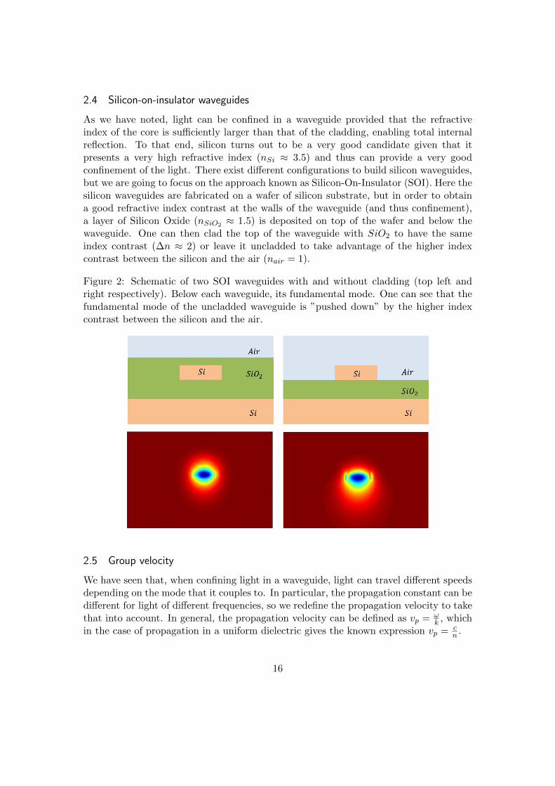
2.4 Silicon-on-insulator waveguides
As we have noted, light can be confined in a waveguide provided that the refractiveindex of the core is sufficiently larger than that of the cladding, enabling total internalreflection. To that end, silicon turns out to be a very good candidate given that itpresents a very high refractive index (nSi ≈ 3.5) and thus can provide a very goodconfinement of the light. There exist different configurations to build silicon waveguides,but we are going to focus on the approach known as Silicon-On-Insulator (SOI). Here thesilicon waveguides are fabricated on a wafer of silicon substrate, but in order to obtaina good refractive index contrast at the walls of the waveguide (and thus confinement),a layer of Silicon Oxide (nSiO2 ≈ 1.5) is deposited on top of the wafer and below thewaveguide. One can then clad the top of the waveguide with SiO2 to have the sameindex contrast (∆n ≈ 2) or leave it uncladded to take advantage of the higher indexcontrast between the silicon and the air (nair = 1).
Figure 2: Schematic of two SOI waveguides with and without cladding (top left andright respectively). Below each waveguide, its fundamental mode. One can see that thefundamental mode of the uncladded waveguide is ”pushed down” by the higher indexcontrast between the silicon and the air.
2.5 Group velocity
We have seen that, when confining light in a waveguide, light can travel different speedsdepending on the mode that it couples to. In particular, the propagation constant can bedifferent for light of different frequencies, so we redefine the propagation velocity to takethat into account. In general, the propagation velocity can be defined as vp = ω
k , whichin the case of propagation in a uniform dielectric gives the known expression vp = c
n .
16

However, in the case of propagation in a waveguide we can redefine it as
vp =ω
β=
c
neff(26)
where we have defined neff = βk0
and we know that β is a function of the frequency.Therefore, for β which is not linear with respect to ω, so is neff a function of thefrequency.
Also, if we consider a pulse of light composed by different frequencies, it can beproved that the velocity at which the envelope travels is
vg =dω
dβ(27)
We can see this if we consider a wave packet as
E(x, t) =
∫ ∞−∞
dkE(k)ei(kx−wt) (28)
where E(k) is the fourier transform of the envelope of the wavepacket. If we assumethat the wavepacket is almost monochromatic, we can linearize the deffinition of ω toyield
ω(k) = ω0 +dω
dk|k=k0∆k = ω0 + ω′0(k − k0) (29)
so that
E(x, t) = eit(w′0k0−ω0)
∫ ∞−∞
dkE(k)eik(x−w′0t) (30)
we find that the absolute value of this expression fulfills
|E(x, t)| = |E(x− w′0t, 0)| (31)
which means that the envelope is travelling at velocity w′0
We can relate the effective index and the group index by noting
1
vg=dβ
dω=
d
dω(k0neff ) =
1
c
d
dω(ωneff (ω)) =
1
c(neff (ω) + ω
dneffdω
) =ngc
(32)
17

2.6 Resonators: Coupled Mode Theory
Another building block of our photonic circuits are microresonators. These are circularstructures that are coupled to a channel so that a fraction of the travelling light entersin the cavity and undergoes several round-trips before leaving it. That induces a buildup of the energy inside the cavity, given that over time more light is coupled to theresonator and can constructively interfere with the previously coupled light if their phasesare matched. Although this phenomenon of resonant enhancement of the field in amicroresonator has been described extensively in the literature ( [8] , [9] ), we are goingto follow most closely Haus’ approach of Coupling of Modes in Time.
One could represent the electromagnetic field in a resonator by writing the electricand magnetic field at some point inside it. However, another alternative is to definea complex quantity a, which we will call the energy amplitude, whose module squarerepresents the energy of the electromagnetic field inside the resonator. In this picture,one can write a differential equation that represents the behaviour of a resonator in thefollowing way
da
dt= jω0a (33)
The solution of this differential equation is a complex exponential oscillating at thefrequency ω0, as we would expect from a resonator. Now, if we want to add the effectof internal losses, we can add a decay term in the following way
da
dt= jω0a− r0a (34)
Finding that the solution to the differential equation is a damped oscillator with adecay rate of r0. Finally, to complete our model of a resonator coupled to a waveguidewe write
da
dt= jω0a− (r0 + re)a− j
√2res+ (35)
Where we have included another decay term re, which represents the internal powerthat is coupled out of the resonator and into the waveguide, and also a driving term√
2res+ which represents the energy that enters in the resonator from the waveguide.Here |s+|2 is normalized to the input power travelling in the waveguide and the cou-pling coefficient
√2re is derived in [9] using arguments of power conservation and time
reversability of Maxwell’s equations. Besides, the fact that there is a π2 phase term
preceding it comes from the physical coupling mechanism between the waveguide andthe ring. Light is coupled from the waveguide to the ring through evanescent coupling,which means that the light that actually propagates through the ring is generated bythe polarization of the material, which consequently radiates. However, this processocurrs with a certain delay, given that the electrons move proportionally to the electricfield, but map this movement to the emission of magnetic field (generalized Amperelaw). Therefore, the electric field caused by the evanescent coupling is always a quarterwavelength delayed from the input electric field.
18

Figure 3: Schematic of a microring with the input and output waves (S+ and S−), thecoupling coefficient and loss rate (re and r0) and the energy amplitude inside the ring, a
If the driving term s+ is at a certain frequency ω, the response will be at the samefrequency, so solving the differential equation in the frequency domain we can find theenergy in the cavity to be
a(ω) =−j√
2res+(ω)
j(ω − ω0) + (re + r0)(36)
which is a Lorentzian response corresponding with other derivations of the spectrumof a resonator. One can also calculate the power amplitude, s− travelling through thewaveguide after the resonator
s− = s+ − j√
2rea = s+(1− 2re(ω − ω0) + re + r0
) (37)
And confirm classical results like the fact that when the ring is critically coupled(when the losses through coupling equal the internal losses) there is no power after theresonator at the resonance frequency.
Here we can also observe that the spectrum of the resonances depend, mainly, on thetwo decay coefficients re and r0. In particular, the total decay coefficient rtot = re + r0is equal to the Half Width at Half Maximum of |a(ω)|2, that is, of the spectrum of theenergy inside the cavity.
19

Figure 4: Spectrum of |a(ω)|2, that is, the energy inside the cavity, for a ring with nointernal losses and a coupling coefficient re = 2. Note that the HWHM coincides withre
-6 -4 -2 2 4 6
0.2
0.4
0.6
0.8
1.0
We can add another channel to the ring that we have just analyzed and it will alreadybehave as a filter. Some frequencies of the input light will couple to the ring and producefield enhancement inside it, therefore being able to couple to the new channel that wehave added and transmitting energy to that output port, which we will call the dropport. On the other side, the frequencies that are not resonant with the ring will arriveto the other end of the waveguide, which we will call the through port, without noticingthe presence of the ring.
To incorporate the presence of a drop channel to our CMT model we just have toadd another decay term, re,2 to the differential equation that describes the evolution ofthe energy amplitude, which corresponds to energy escaping from the ring through thenew coupler. On the other side, we can now add an output S2,− which represents theenergy that is coupled to the drop channel. In the end, our CMT equations have become
da
dt= jω0a− (r0 + re,1 + re,2)a− j
√2re,1s1,+ (38)
S1,− = S1,+ − j√
2re,1a (39)
S2,− = −j√
2re,2a (40)
20
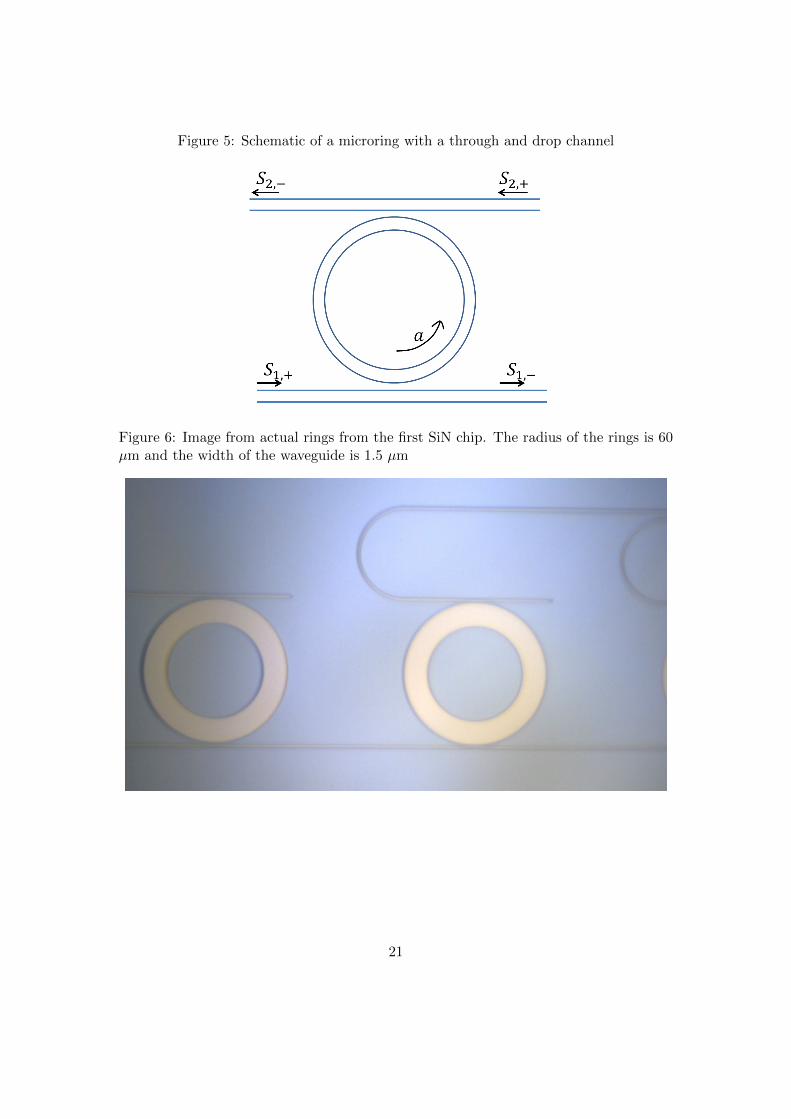
Figure 5: Schematic of a microring with a through and drop channel
Figure 6: Image from actual rings from the first SiN chip. The radius of the rings is 60µm and the width of the waveguide is 1.5 µm
21
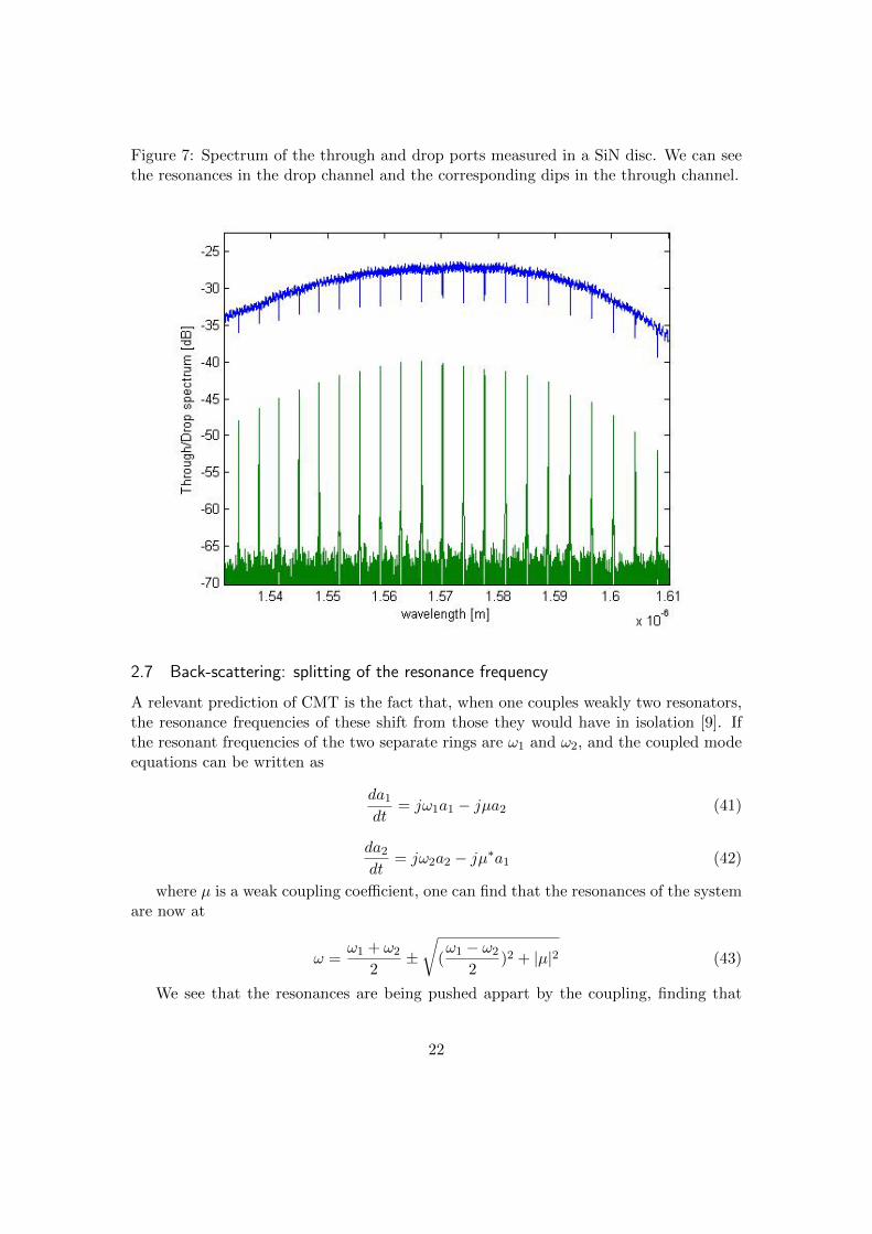
Figure 7: Spectrum of the through and drop ports measured in a SiN disc. We can seethe resonances in the drop channel and the corresponding dips in the through channel.
2.7 Back-scattering: splitting of the resonance frequency
A relevant prediction of CMT is the fact that, when one couples weakly two resonators,the resonance frequencies of these shift from those they would have in isolation [9]. Ifthe resonant frequencies of the two separate rings are ω1 and ω2, and the coupled modeequations can be written as
da1dt
= jω1a1 − jµa2 (41)
da2dt
= jω2a2 − jµ∗a1 (42)
where µ is a weak coupling coefficient, one can find that the resonances of the systemare now at
ω =ω1 + ω2
2±√
(ω1 − ω2
2)2 + |µ|2 (43)
We see that the resonances are being pushed appart by the coupling, finding that
22
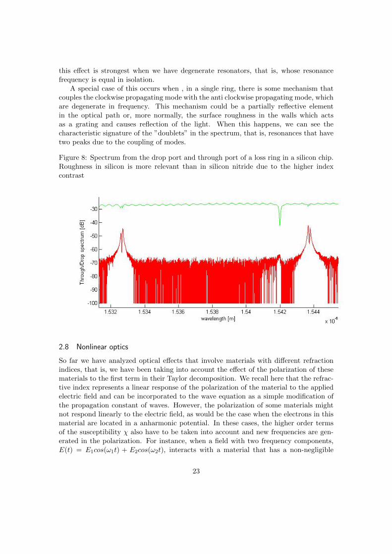
this effect is strongest when we have degenerate resonators, that is, whose resonancefrequency is equal in isolation.
A special case of this occurs when , in a single ring, there is some mechanism thatcouples the clockwise propagating mode with the anti clockwise propagating mode, whichare degenerate in frequency. This mechanism could be a partially reflective elementin the optical path or, more normally, the surface roughness in the walls which actsas a grating and causes reflection of the light. When this happens, we can see thecharacteristic signature of the ”doublets” in the spectrum, that is, resonances that havetwo peaks due to the coupling of modes.
Figure 8: Spectrum from the drop port and through port of a loss ring in a silicon chip.Roughness in silicon is more relevant than in silicon nitride due to the higher indexcontrast
2.8 Nonlinear optics
So far we have analyzed optical effects that involve materials with different refractionindices, that is, we have been taking into account the effect of the polarization of thesematerials to the first term in their Taylor decomposition. We recall here that the refrac-tive index represents a linear response of the polarization of the material to the appliedelectric field and can be incorporated to the wave equation as a simple modification ofthe propagation constant of waves. However, the polarization of some materials mightnot respond linearly to the electric field, as would be the case when the electrons in thismaterial are located in a anharmonic potential. In these cases, the higher order termsof the susceptibility χ also have to be taken into account and new frequencies are gen-erated in the polarization. For instance, when a field with two frequency components,E(t) = E1cos(ω1t) + E2cos(ω2t), interacts with a material that has a non-negligible
23

second order susceptibility χ(2) the polarization has the form
P (t) = ε0(χ(1)E(t) + χ(2)E2(t)) (44)
which introduces cross terms between the two frequency terms, including componentsat the sum and difference frequencies. In these cases, a more general wave equation isobtained [6]
∇2 ·En(r) +ω2nε
(1)(ωn)
c2En(r) = − ω2
n
ε0c2PNL
n (r) (45)
Here we have assumed that the time dependence of the electric field can be decom-posed in harmonic components and are analyzing a single frequency term ωn, so we havesubstituted the time derivative for its equivalent in frequency domain. Also, we have toidentify the term PNL
n as the polarization terms at a frequency ωn.This equation has to be fulfilled for all frequencies, so this creates a system of coupled
differential equations that allow us to find the solutions for the electric field and quantifythe energy transfer that occurrs between the different frequency components.
2.9 The photon picture of nonlinear optics
Besides the wave equation description that we gave of nonlinear optics, quantum opticsalso offers its explanation of how these processes occurr. Without intending to make anin depth analysis of this, we will briefly give a very simple and useful picture of nonlineareffects as a result of energy conservation in a process where photons are absorbed anemitted. Since the inception of quantum physics, scientists realized that light was trans-mitted in discrete units of energy that we call photons, whose energy content is directlylinked to their frequency. In particular, the energy of a photon is E = hν, where h isPlanck’s constant and ν is the frequency. Now, if for instance an atom gains a certainamount of energy by absorbing a photon of a certain frequency, it can either release theenergy by emitting the photon back or by emitting two photons of energies (and thereforefrequencies) such that their sum equals that of the absorbed photon. The process thatwe just described is called Parametric Down Conversion and describes the conversion ofa single energetic photon to a pair of photons with lower energy. The opposite processcan also happen, in which an atom absorbs two photons and emits a single photon withenergy equal to the sum, and corresponds to Frequency Sum Generation.
24

Figure 9: Diagrams showing Parametric Down Conversion (left) and Frequency SumGeneration (right)
2.10 Phase matching
Phase matching is a very important concept in nonlinear optics and refers to the fact that,for frequency conversion to take place, not only energy conservation has to be fulfilled,but also the different interacting waves need to have k vectors (momentums) that alsofulfill certain relations. For instance, in the process of Frequency Sum Generation (FSG),themomentum mismatch ∆k = k1+k2−k3 has to be as small as possible for the frequencyconversion to be efficient. In fact, the efficiency of a FSG process in a homogeneousmaterial occurring during a distance L is proportional to sinc(∆kL/2) [6], where wecan see that the phase matching condition becomes more and more restrictive as theconversion length L increases. We can imagine this as having the input waves (and thusthe polarization of the material) and the generated wave slowly shift out of phase, whichcauses power to be able to flow back from the ω3 wave back into the ω1 and ω2 waves.
To obtain a small momentum mismatch is not easy because most lossless materialsexhibit an effect known as normal dispersion, which consists of a frequency dependentrefractive index which is increasing as a function of frequency. Therefore, whereas in freespace energy matching would imply momentum matching, in this case the momentummismatch can be written as
∆k =n1ω1
c+n2ω2
c− n3ω3
c(46)
and depends on the refractive indices for the different frequencies. This phenomenonis compensated in bulk materials by using a procedure known as Periodically Poling,which consists in changing the sign of the nonlinear susceptibility of the material pe-riodically so that the period coincides with the length at which the input and outputwaves get out of phase. In this way, instead of having the energy flow back to the inputwaves, the frequency conversion process continues thanks to the susceptibility havingthe opposite sign. On the other side, integrated optics offer a different mechanism tocompensate for dispersion. As we have noted above, guided modes might have a different
25

group velocity depending on their frequency due to their different confinements. Thiswaveguide dispersion can be engineered to have a sign opposite to the normal disper-sion, i.e. so that the group index diminishes with frequency, which is called anomalousdispersion [10]. When this is possible, one can design waveguides in such a way thatthese two dispersions compensate each other, at least for certain wavelengths.
2.11 Four Wave Mixing
The processes that we just described used the second order susceptibility to induce aninteraction between three waves. This is normally the strongest nonlinear interactiongiven that nonlinear susceptibility terms become smaller as their order increases. As arule of thumb, the strength of each term of the susceptibility is around 12 orders of mag-nitude lower than that of the previous order term. Therefore we would expect χ(2) to bealways used in nonlinear optics experiments, as the next nonlinearity is much smaller,but unfortunately it is not true that all materials present a second order nonlinearity.In fact, it can be proved that a material requires to be non-centrosymmetric in order tohave a χ(2), which is not the case in many crystals or amorphous glasses. In particular,neither silicon nor silica, which are the most used materials in the fabrication of opti-cal waveguides or fiber optics, posses inversion assimetry, and therefore are not usefulfor χ(2) nonlinear optics experiments. However, these materials do have a third ordernonlinearity which, thanks to our hability to confine optical field in very small modevolumes and therefore obtain very large intensities, we can still use to observe nonlineareffects.
One of the most important nonlinear phenomenon that we can observe with a χ(3)
material is known as Four Wave Mixing (FWM). In it, the cubic nonlinearity generatesfrequencies that are a combination of three of the input frequency components. Aparticular case of this is known as degenerate pump four wave mixing, and occurs whenwe shine a strong pump beam of frequency ωp into a χ(3) nonlinear material. In thisscenario, light will be generated at pairs of frequencies that fulfill ωi + ωs = 2ωp andwhich we will call the signal and idler beams. If we look at this process using the photonpicture, we can understand it as a system that absorbs two photons of the pump beamand afterwards releases two more photons such that their compound energy is the samethat it had absorbed.
26
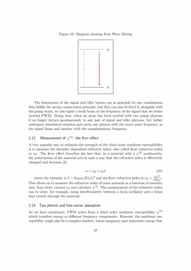
Figure 10: Diagram showing Four Wave Mixing
The frequencies of the signal and idler beams can in principle be any combinationthat fulfills the energy conservation principle, but they can also be fixed if, alongside withthe pump beam, we also input a weak beam at the frequency of the signal that we desire(seeded FWM). Doing that, when an atom has been excited with two pump photonsit no longer decays spontaneously to any pair of signal and idler photons, but ratherundergoes stimulated emission and emits one photon with the exact same frequency asthe signal beam and another with the complementary frequency.
2.12 Measurement of χ(3): the Kerr effect
A very popular way to estimate the strength of the third order nonlinear susceptibilityis to measure the intensity dependent refractive index, also called Kerr refractive indexor n2. The Kerr effect describes the fact that, in a material with a χ(3) nonlinearity,the polarization of the material acts in such a way that the refractive index is effectivelychanged and becomes [6]
n = n0 + n2I (47)
where the intensity is I = 2n0ε0c|E(ω)|2 and the Kerr refractive index is n2 = 3χ(3)
4n20ε0c
.
This allows us to measure the refractive index of some material as a function of intensityand, from there, extract n2 and calculate χ(3). The measurement of the refractive indexcan be done, for example, using interferometry between a local oscillator and a beamthat travels through the material.
2.13 Two photon and free-carrier absorption
As we have mentioned, FWM arises from a third order nonlinear susceptibility χ(3)
which transfers energy to different frequency components. However, the nonlinear sus-ceptibility might also be a complex number, whose imaginary part represents energy that
27

is absorbed by the material through a nonlinear process like, for instance, two photonabsorption (TPA). [11] Silicon is transparent at telecom wavelengths, that is, it doesnot absorb photons that travel through it, because its bandgap is wider than the energythat a photon at that wavelength can contain. For that reason, photons are not able topromote electrons from the valence band to the conduction band and the energy remainsin the optical field. However, the optical field is intense enough inside the material, thiscan absorb a pair of photons simultaneaously and promote an electron to the conductionband. This gives rise to the so called TPA and is an important source of optical loss athigh intensities. The amount of TPA that occurs in the material also decreases when weuse even longer wavelengths, given that photons are less energetic at those wavelengthsand eventually a pair of photons is not enough to drive an electron all the way throughthe band gap. The value of the real and imaginary part of the χ(3) susceptibility ofsilicon have been measured by different groups ([12], [13]) and have been shown to havea different frequency dependency. Whereas n2 stays rather constant for wavelengths inthe optical range, TPA rolls off for long wavelengths and becomes almost negligible forwavelengths above 2µm.
2.14 Optical Parametric Oscillation
In this work we are going to analyze a type of systems called Optical Parametric Os-cillators (OPOs), which consist of a frequency conversion process (in our case FWM)occurring inside an optical cavity. The effect of the optical cavity is to produce feed-back to the FWM process so, above a certain threshold of the pump power, most ofthe light that is created inside the cavity is not due to Spontaneous Four Wave Mixing(SFWM) but is seeded by the signal and idler that has been previously generated. Thissituation resembles very much the operation of a laser below and above threshold, whereabove some pump power certain frequency modes predominate over the others and theemission of light becomes nearly monochromatic. To analyze this phenomenon we aregoing to use again Coupled Mode Theory to quantify how the energy transfer betweenthe different modes occurs and at what pump power the signal and idler have enoughfeedback to start ”lasing”.
We are going to analyze the case where just three resonances are involved in theFWM process (pump, signal and idler), which is a valid assumption if our resonatoris dispersion engineered so that the phase matching condition is only fulfilled for tworesonances.
28

We use a reduced version of the CMT model developed by Zeng et al. [2] where weomit the effects of two photon absorption and free-carrier absorption.
δAsδt
= −(rext,s + r0,s)As − jωβA2pA∗i (48)
δAiδt
= −(rext,i + r0,i)Ai − jωβA2pA∗s (49)
δApδt
= −(rext,p + r0,p)Ap − j2ωβA∗pAsAi − j√
2rext,pSp,+ (50)
Ss,− = −j√
2rext,sAs (51)
Si,− = −j√
2rext,iAi (52)
Sp,− = Sp,+ − j√
2rext,pAp (53)
In the following sections we will use these CMT equations to derive useful informationabout an OPO driven by FWM, such as the oscillation threshold, the energy stored insidethe cavity or the output power in the different modes.
29
3 A Silicon Nitride platform: fabrication and characterization
3.1 Motivation
The main motivation that drives this work is to develop quantum optics experimentsin an integrated optics platform. However, the quantum nature of light can only beobserved in very fragile features, that are destroyed very quickly in the presence of loss.For this reason, it is critical to develop integrated optics circuits that exhibit very lowloss in all of their components (waveguides, microrings, couplers, etc.). In this respect,TPA in silicon really hinders the realization of quantum states of light with a largenumber of photons, given that the high intensities trigger the TPA process and thusthe loss. One possible way to avoid this is, as we said before, to work at wavelengthsbeyond 2µm, but this is not desirable because the best optical components are currentlyfabricated at telecom wavelengths. For instance, one would like to take advantage of theexistence of high quantum efficiency photodetectors at those wavelengths.
Another way to avoid TPA is to use a different material, and to that end siliconnitride has proven to be a promising candidate for integrated nonlinear optics.
3.2 Optical properties of Silicon Nitride
An advantage of silicon nitride with respect to silicon is that the first is a dielectricmaterial without a conduction band, which prevents the unwanted effect of two photonabsorption. This is the main reason why we have chosen to use it instead of silicon.
The refractive index of silicon nitride obeys the following Sellmeier equation [14]
nSiN =
√1 +
2.8939λ2
λ2 − 0.139672(54)
and so we see that at telecom wavelengths its refractive index is of the order ofnSiN = 2, which gives us a smaller index contrast than silicon but still allows goodconfinement provided that the waveguides are big enough.
On the other side, the intensity dependent refractive index of silicon nitride is [2]n2 = 2.4 × 10⁻¹⁹m2/W , one order of magnitude below that of silicon. This drawbackis compensated by the great field enhancement that one can achieve in microresonatorsand the fact that we can pump with high powers.
3.3 A low loss Si3N4 platform
One of the most crucial features of our optical circuits is that they should be extremelylow loss, given that loss is one of the mechanisms that hinders most the observationof nonclassical features. In first place, the silicon nitride that we use should be totallytransparent at telecom wavelengths, which is only achieved in high purity Si3N4 whichdoes not contain hydrogenated silicon nitride. In the case when hydrogen is present,the bonds between Si-H and N-H create absorption peaks close to telecom wavelengths[15] which degrade the performance of our devices. Specially harmful is the N-H bond,whose absorption tail causes loss in the region of 1510-1565 nm.
30
We are provided of high purity Si3N4 by a company called LioniX, who fabricatethe nitride wafers through Low Pressure Chemical Vapour Deposition (LPCVD). Thedrawback of nitride is that it has an intrinsically high film stress which causes that,beyond a certain thickness of the film, cracks start to appear and propagate [16]. Forthis reason, the wafers provided by LioniX are limited to a thickness of 220 nm of denseSiN, which are deposited on top of 8 microns of SiO2 on top of a silicon substrate.
These wafers are now sent to the Nanofabrication Facility at the University of Wash-ington, where our designed circuits are written through e-beam lithography and sentback to Colorado for characterization.
Another major source of loss comes from the fact that the walls of the fabricatedwaveguides are not perfectly smooth, but have a certain roughness due to differentimperfections in the fabrication process. This roughness acts as a kind of diffractiongrating and couples the propagating mode to radiation modes, which are effectivelyseen as loss. To characterize the amount of loss that we have in our waveguides (whichincludes material loss, radiation loss and other mechanisms), we design a set of microringresonators that will be very weakly coupled to the bus waveguide. In this way, thelinewidth of their resonances will be determined, mostly, by the internal losses ratherthan by the coupling to the waveguide, and therefore we will be able to infer the lossesfrom this measurement. To do this measurement we are interested in having a couplingas weak as possible, so that virtually only the losses determine the linewidth of theresonances, but at the same time there is a tradeoff with the level of the signal thatone will receive. Too weak a coupling will leave us with no light to measure. Anoptimum design of loss rings exists [17] which will determine the smallest set of rings wecan use to measure optimally the intrinsic Q while mantaining the signal level above acertain threshold. Using this approach we are able to measure the drop port transmisionspectrum of a set of rings and, fitting the results to a CMT model, derive the decayparameter r0 which will then give us the internal quality factor of the resonator.
31

Figure 11: (a) Layout of the loss rings used to measure the intrinsic quality factor ofthe rings. This layout shows two sets of loss rings with different widths of the rings.On the top set, light is pumped from the right hand port and collected in the ports ofthe left. (b)Spectrum of the loss rings at different ports. The first ring (drop 1) is themost coupled, so the linewidth of the resonance is dominated by the coupling decay re.The third ring (drop 3) is the least coupled, so its linewidth gives a good estimate of theintrinsic quality factor
Besides, when designing microrings, one has to make sure that the radius of thering is not too small. In general, the curving of the waveguide to form a ring has theeffect that the mode is ”pushed against the outer wall” similarly to what happens withcentripetal forces. If the radius becomes too small, part of the mode will be pushed awayfrom the waveguide and radiated. Equivalently, for a fixed radius, if we use too large
32

a wavelength, the mode will become bigger and thus less confined, so the losses due tobending radiation will become bigger. To avoid this effect, one does simulations with amode solver to find the minimum bending radius so that the intrinsic quality factor isnot determined by radiation loss.
In our design we have included two sets of loss rings. The minimum radius thatguarantees a bending loss Q greater than 107, that is, large enough so that it does notinfluence the linewidth, is 60 microns. The couplings are chosen optimally to characterizethe internal losses, and the width of the bus waveguide is chosen so that it supports onlya single mode. The difference between the two sets of rings is their radius. The firstset has a radius of 1.5 microns, which only supports a single mode, whereas the secondset has a ring width of 20 microns. This second set is designed to behave more like amicrodisk rather than like a ring. That means that it is going to be so wide that theoptical mode is not going to be affected by the inner wall. These modes are usuallycalled ”whispering gallery resonator” modes because their guiding is produced only bytotal internal reflection in the outer wall of the waveguide. The intrinsic Q of the lossdisks is likely to be greater than that of the rings because of the absence of interactionof the optical mode with the inner wall, therefore avoiding the scattering produced bythe its roughness.
We measure the intrinsic Qs of both loss disks and loss rings and obtain an averagequality factor of 530 K for the rings and 800 K for the disks. These are very high qualityfactors and in fact are of the order of magnitude of the achieved by state of the artsilicon nitride microdisk resonators ([18] , [19])
Our insertion loss, calculated as the power in the photodetector divided by the outputpower of our laser when pumping out of resonance, is of 15 dB. That includes all thepropagation and detection losses, but can be attributed mainly to the grating couplerinefficiencies, which are the main cause of loss in our system. Therefore, we can estimatea grating coupler loss of approximately 7dB.
3.4 Geometry control
It is also essential that the fabricated structures are close enough to the geometry ofthe nominal design in orderto obtain the expected optical performance. For instance,when doing FWM, there is a very delicate interplay between the width, radius andthickness of the microring that determine the dispersion of the ring, and which we haveto accurately engineer in order to get the maximum possible conversion efficiency. Avery useful method to assess that the fabricated dimensions agree with the design is touse a Scanning Electron Microscope (SEM). This technique consists in shining a beam ofelectrons on a sample instead of an optical beam and, thanks to the smaller wavelengthof the former, obtain a better resolved image. Samples are first coated in a conductivematerial (in this case gold) so that they do not get charged while imaging them withthe electron beam. Using this method, one can resolve horizontal features as small as afew nanometers, which totally allow us to characterize features of our chips such as thewaveguide width or the ring radius.
33
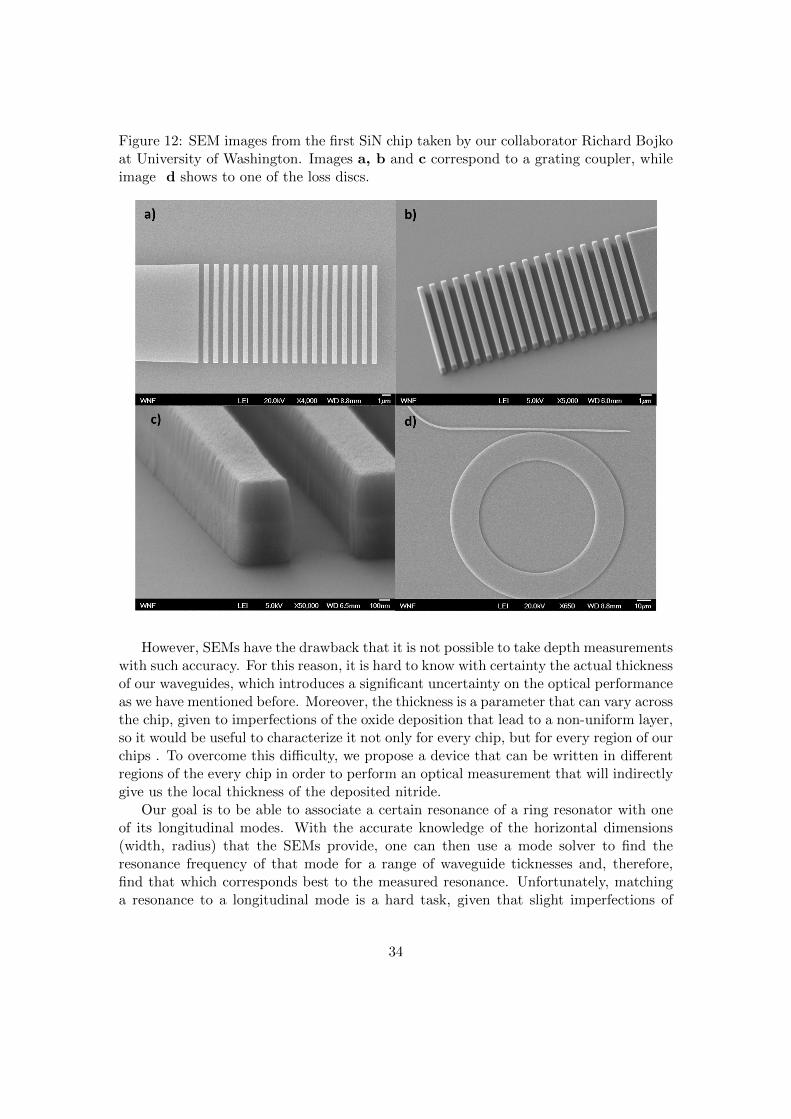
Figure 12: SEM images from the first SiN chip taken by our collaborator Richard Bojkoat University of Washington. Images a, b and c correspond to a grating coupler, whileimage d shows to one of the loss discs.
However, SEMs have the drawback that it is not possible to take depth measurementswith such accuracy. For this reason, it is hard to know with certainty the actual thicknessof our waveguides, which introduces a significant uncertainty on the optical performanceas we have mentioned before. Moreover, the thickness is a parameter that can vary acrossthe chip, given to imperfections of the oxide deposition that lead to a non-uniform layer,so it would be useful to characterize it not only for every chip, but for every region of ourchips . To overcome this difficulty, we propose a device that can be written in differentregions of the every chip in order to perform an optical measurement that will indirectlygive us the local thickness of the deposited nitride.
Our goal is to be able to associate a certain resonance of a ring resonator with oneof its longitudinal modes. With the accurate knowledge of the horizontal dimensions(width, radius) that the SEMs provide, one can then use a mode solver to find theresonance frequency of that mode for a range of waveguide ticknesses and, therefore,find that which corresponds best to the measured resonance. Unfortunately, matchinga resonance to a longitudinal mode is a hard task, given that slight imperfections of
34

our fabrication might already make it shift by more than an FSR, therefore making itimpossible to tell one mode from the next or the previous with certainty.
3.4.1 A device for absolute frequency reference
To overcome this, we propose to introduce a slight sinusoidal modulation of the width ofthe ring so that, in the same way as a grating works, only the light whose wavelength istwice the period of the modulation will be affected constructively by the perturbation,causing reflection of the light. This reflection, or coupling to the counter-propagatingmode, has the same resonance frequency as the forward-propagating mode, and thuswill be coupled to this and lead to the splitting of the resonance frequency that ischaracteristic of degenerate coupled modes. In this way, we will be able to recognizethat a certain peak of the spectrum of the ring corresponds to a certain longitudinalmode and from then calculate the actual thickness of the waveguide.
Figure 13: Layout of the ring with modulated width. The amplitude of the modulationis here exagerated for illustration purposes
3.4.2 Perturbation theory
When a resonant optical system undergoes a slight change in its refractive index prop-erties, a coupling between different modes occur through the polarization currents beingable to radiate in different modes other than the original. This couplings can be foundthrough perturbation theory methods using the overlap integral ([32], [9],[37])
µi,k =≈ −ω2
∫dV (∆Pi(r))∗Ek(r)∫dV ε(r)|Ei(r)|2
= −ω2
∫dVE∗i (r)∆ε(r)Ek(r)∫dV ε(r)|Ei(r)|2
(55)
However, although in the scenario that we are considering there is indeed a smallperturbation of the system, the change of refractive index happens in large jumps due tothe moving interfaces so the previous approach is no longer appropiate. In the cases when
35

a boundary between two dielectrics is slightly moved, the perturbation of the refractiveindex only occurs in a small region around the boundary, so we can effectively substitutethe volume integration for a surface integration, and multiply this by the displacementof the boundary. Doing this we are approximating the electric field in the perturbedregion with the electric field in the surface. However, a problem arises, which is thatthe electric field is discontinuous when there is a sharp boundary, so it is not possible toassign a value to the electric field at the interface itself. To avoid this problem, we canuse the D vector instead, which has to be continuous [33]. Thus, we can substitute theprevious expression by
µi,k ≈ −ω
2
∫d2r[E∗i,||∆εEk,|| −D
∗i,⊥∆(1/ε)Dk,⊥]∆h∫
dV ε|Ei(r)|2(56)
where we have separated the electric field in the components tangential and perpen-dicular to the wall and substituted the electric field by the D vector in the later. Theshift of the boundary is taken into account in the term ∆h.
3.4.3 Coupling to the counterpropagating mode
Now we are going to apply the previous ideas to the case of coupling the clockwisepropagating mode (Ecw) to the counter-clockwise propagating mode (Eccw). Because ofthe symmetry, these two modes have the same mode profile and only difer in the spatialphase. Expressed in cylindrical coordinates we can write them as
Ecw ≈ E0(r, z)ej(ωt−βθr0) = E0(r, z)e
j(ωt−γθ) (57)
Eccw ≈ E0(r, z)ej(ωt+βθr0) = E0(r, z)e
j(ωt+γθ) (58)
Also, in the limit when the perturbation of the wall is very small we can take theoverlap integral only in the boundary and multiply by ∆h. When the perturbation is asinusoidal modulation of the wall we can write the coupling as
µi,k ≈ −ω
2
∫ ∫dθdz[|E0,||(r0, z)|2∆ε− |D0,⊥(r0, z)|2∆(1/ε)]r0Acos(Γθ)e
j2γθ∫dV ε|Ei(r)|2
(59)
= −ω2
∫dz[|E0,||(r0, z)|2∆ε− |D0,⊥(r0, z)|2∆(1/ε)]r0A
∫dθcos(Γθ)ej2γθ∫
dV ε|Ei(r)|2(60)
The second integral of this equation can be readily evaluated and corresponds to twosinc functions, which only take nonzero values for natural Γ = 2γ
36
µi,k ≈ −ωπAr0
2
∫dz[|E0,||(r0, z)|2∆ε− |D0,⊥(r0, z)|2∆(1/ε)]∫
dV ε|Ei(r)|2= (61)
= −ωπAr02
∫dz[|E0,||(r0, z)|2∆ε− |D0,⊥(r0, z)|2∆(1/ε)]
2πr0∫dAε|Ei(z, r)|2
= (62)
= −ωA4
∫dz[|E0,||(r0, z)|2∆ε− |D0,⊥(r0, z)|2∆(1/ε)]∫
dAε|Ei(z, r)|2(63)
37
4 A quantum application: Twin beam generation
4.1 Motivation
To date, the workhorse of photon pair generation for quantum optics experiments hasbeen Spontaneous Parametric Down Conversion, given that it uses the first, and thusstrongest, nonlinearity of the optical susceptibility. However, other terms of the nonlinearpolarization of a material can be used to generate pairs of photons and, in particular, itis sometimes necessary to turn to them when our nonlinear material is centrosymmetricand, thus, doesn’t have a second order nonlinearity. This is the case, for instance,when you want to integrate quantum optics experiments on a silicon nitride chip, inorder to achieve scalability and higher complexity. Silicon nitride does not show asecond order susceptibility, so to perform nonlinear optics in it one has to exploit its χ(3)
nonlinearity. The advantage of using this material, however, is that one can build verygood waveguides and resonators that can confine the electromagnetic field in very smallregions, thus achieving a high intensity and enhanced nonlinear effects.
In particular, one experiment that still hasn’t been very thoroughly described is thegeneration of squeezed light on an on-chip resonator. Squeezed light generation hasbeen very well documented in bulk optics experiments and even in fiber optics, but acomplete description of the process in integrated resonators seems to be still pending tobe done. That structured description might be useful for anyone who intends to pursueexperiments in the field, so that he can have an overview of which are the physicalprinciples ruling here and, specially, what are the main design parameters with whichone can play to achieve better performance.
4.2 Brief introduction to squeezed light
Since the discovery that light is transmitted in discrete quantums of energy, the photons,the nature of the electromagnetic field has been reconsidered and a new formalism hasbeen needed to convey its quantum features. The study of the nonclassical effects thatlight can exhibit is called quantum optics, and it is a very broad topic which requiresa good deal of new mathematical tools which we will not be able to describe in detailhere. However, it will be usefull to introduce some of the concepts of quantum opticsmost relevant to our discussion. A comprehensive introduction to quantum optics canbe found in the books by Walls and Milburn, Scully and Zubairy or Cohen-Tannoudji( [20], [21], [22]). Our introduction draws from these texts among others ([24], [23],[25],[26]).
The first step when building a quantum theory of light is to quantize the electromag-netic field. The electromagnetic field can be decomposed as a superposition of differentmodes, each of which has an harmonic evolution in time. In that sense, each of themodes of the electromagnetic field can be thought of as an harmonic oscillator, but onethat behaves according to the rules of quantum physics. We will start by introducing thequantum harmonic oscillator and relate it to a single mode of the electromagnetic field.After this, we will understand how we describe the quantized electromagnetic field.
38

An harmonic oscillator is a system governed by an equation of motion of the type:
md2x
dt2= −kx (64)
d2x
dt2= −w2x (65)
This equation of motion is derived, in classical mechanics, from the Hamiltonian
H =mw2
2x2 +
1
2m(dx
dt)2 =
mw2
2x2 +
1
2mpx
2 (66)
which expresses the energy contained in the system as the sum of potential andkinetic energy.
In quantum mechanics, however, the position and momentum of the particle cannotbe expressed as definite variables, but as operators whose eigenvalues correspond tothe observable quantities that we can measure. One of the main differences betweenclassical and quantum mechanics arises when we try to solve the eigenvalue problem forthe hamiltonian of the harmonic oscillator (substituting the position and momentumvariables by its correspondent operators), which would give us its allowed energy states.The quantum hamiltonian reads
H = (− h
2m
d2
dx2+mω2
2x2) (67)
And therefore the equation
H|ψ >= E|ψ > (68)
corresponds to the Schrodinger equation.Surprisingly, this problem does not have a continuous spectrum (space of the solu-
tions), but a discrete one. This means that the harmonic oscillator cannot contain anarbitrary amount of energy, but has to be excited through discrete jumps. We see nowthe analogy between a quantum harmonic oscillator and the quantized electromagneticfield. Two very important operators are now introduced, the creation and annihilationoperators, which will be fundamental to deal with quantum optical fields. If we expressthe hamiltonian in terms of two new operators
a =1√2
(
√h
mω
d
dx+
√mω
hx) (69)
a† =1√2
(−√
h
mω
d
dx+
√mω
hx) (70)
we obtain
H = hω(a†a− 1/2) (71)
39
and the commutation relation
[a, a†] = aa† − a†a = 1 (72)
These operators have the particularity that, when applied to a quantum state, theyeither lower or increase the eigenvalue of the hamiltonian equation by a quantum ofenergy, therefore the reason of the names “annihilation” and “creation” operators, giventhat they add or substract a photon from the field. The result of applying the creationoperator on a field with n photons is a field with n+ 1 photons
a†|n >=√n+ 1|n+ 1 > (73)
Thus one can write a field with a certain amount of photons (a Fock state) by applyingmany times the creation operator on the vacuum state.
|n >=(a†)n√n!|0 > (74)
Surprisingly one also finds that the eigenvalue of the hamiltonian equation for thevacum state |0 > is not zero, but hω/2. This means that the electromagnetic field cannotbe in a state of zero energy, but has some vacuum fluctuations.
Fock states are a very particular subset of the possible quantum states of the elec-tromagnetic field, but all states can be expressed in the photon number basis, that is, asa linear combination of Fock states. For instance, a coherent state can be expressed as
|α >= e−|α|2/2
∞∑n=0
αn√n!|n > (75)
Although the photon number basis is extremely useful when one wants to describenonclassical behaviour that happens at the single photon level (e.g. Hong-Ou-Mandelinterference), it is not very convenient when describing states with a large number ofphotons, given that one has to give the amplitude and the phase of every Fock statecomponent. In these cases, one can turn to the continuous variables approach, in whichone does not make reference to each photon in the field, but to macroscopic observablescalled the quadratures of the electromagnetic field.
In the quantum picture, the electric field is described by the following operator
E(r, t) = i∑k,α
√hωk
2ε0L3(eαak,αe
i(kr−ωkt) − e∗αak,α†ei(−kr+ωkt)) (76)
where the subindex k refers to the different spatial modes, α refers to the two po-larizations and L is the quantization volume, which would be the volume of a certaincavity when the field is confined or can be made arbitrarily large when dealing with freespace propagation.
Expressing the electric field with two quadratures means doing the following decom-position
40

E(r, t) = i∑k,α
√hωk
2ε0L3(X1sin(ωt− kr) + X2cos(ωt− kr)) (77)
So that the quadratures can be expressed in terms of creation and annihilation op-erators like
X1 = a+ a† (78)
X2 = i(−a+ a†) (79)
Or in fact one can generalize the definition of the quadratures to represent the electricfield at an arbitrary phase
Xθ =1√2
(ae−iθ + a†eiθ) (80)
These quadratures, unlike the classical quadratures of the electric field, do nothave a determined value but are operators. One can, however, find the average valueand the variance of these operators when acting on a certain state, or even plot a(quasi)probability density function for them. We have added the prefix quasi becausequantum states cannot be defined merely by probability distributions, and thereforeone has to use functions that resemble very much a probability distribution but whichcan also take negative values. One example of these quasiprobability functions is theWigner function, which is defined as the Fourier transform of the characteristic functionξ(k) = 〈eikXθ〉, which classically would correspond to the probability density functionfor a certain quadrature. However, in this case, the averaging in the transfer function iscarried out follwing the formalism of quantum mechanics and thus the Wigner functionneed not fulfil certain restrictions of a classical probability function, like for instance theneed to be positive in all of its domain. In fact, if one computes the Wigner function fora single photon state, it has a negative dip in the origin which is a characteristic markof its nonclassicality.
In the case of a coherent state, however, the wigner function is essentially a gaussiandistribution with a mean that corresponds to the classical value of the electromagneticfield. The variance of the distribution, unlike in the classical case, cannot be madearbitrarily small, but is limited by the Heisenberg uncertainty principle. In the same waythat the position and momentum of a quantum object cannot be simultaneously knownwith perfect accuracy, the two quadratures of the electromagnetic field are also subjectto a total uncertainty relation that has to be conserved. In this case the uncertaintyrelation reads ∆X1∆X2 ≥ 1. Incidentally, the coherent state is a minimum uncertaintystate, which means that it fulfils the uncertainty relation with the equality, and moreover,one where the two uncertainties are equal.
41

Figure 14: Wigner function of a coherent state
However, a broader class of gaussian states exist which are called squeezed states.These states are also represented by two-dimensional gaussians in their Wigner functions,but the variances of their quadratures are not needed to be equal. This means that,although the uncertainty principle still has to be fulfiled, some quadratures of the electricfield can have a variance reduced with respect to a coherent state. In fact, observingsuch reduced variance provides us with the signature of a nonclassical squeezed state.The variance exhibited by a quadrature of a coherent state sets a threshold called theStandard Quantum Limit (SQL), which separates classical from quantum behaviour. Astate showing fluctuations below the SQL will have nonclassical correlations.
These states have traditionally been generated by nonlinear optical processes wherethe nonclassical correlations between the generated photons are responsible for the re-duced fluctuations of a certain observable. In particular,OPOs based on ParametricDown Conversion have been a very used resource to produce indistinguishable photonpairs and squeezed light. Lately the pair generation rate and the purity of the states havebeen enhanced by integrating the nonlinear medium and the cavity in a single crystalor waveguide ([27], [28], [29] ) .
42

Figure 15: Wigner function of a squeezed state
In this work we will be concerned about a particular subset of squeezed states calledtwo-mode squeezed states. In these states two different optical modes are involved (ofdifferent frequencies or polarizations for instance), so that nonclassical effects are notpresent when one observes one isolated mode but rather when one takes into accountcorrelations between photons in the two modes. These kind of correlations were firstdiscused in the famous paper by Einstein, Podolsky and Rosen (EPR), where theyargued that quantum mechanics must be an incomplete theory given that it wouldallow ”spooky instantaneous action at a distance” in these kind of correlated systems[30]. While in single mode squeezed states we can say that a particular quadrature ofthe field is squeezed, meaning that its fluctuations will be below the SQL, in a two modesqueezed state it will be the difference or sum of the quadratures of two different modesthat will exhibit reduced uncertainty. For instance, if we define X1 and P1 to be thetwo quadratures of a mode and X2, P2 the quadratures of another mode, the observableX1 − X2 might be squeezed. In this way, when one observes X1 the value of X2 willbe determined within a greater accuracy than what classical knowledge would allow.Therefore, the measurement of one of the modes would somehow collapse the state ofthe other mode to a certain value instantaneously, even if they have been brought veryfar away one from the other.
43

4.3 Coupled mode theory derivation of squeezing
Degenerate-pump Four Wave Mixing is a process in which two pump photons of the samefrequency are converted to another pair of photons of frequencies dictated by energyconservation. In this process, the signal and idler photons have different frequencies,so the output pairs of photons are not indistinguishable. In this sense, the output ofa squeezer driven by degenerate-pump FWM cannot be a single mode squeezed state.However, the composite system formed by the two output beams is certainly nonclassicaland can be described as a two-mode squeezed state.
There are many ways in which a state can be squeezed, from amplitude to phasesqueezing through a variety of combinations. In a two mode squeezed state, there arealso different observables whose uncertainty can be reduced, one of them being theintensity difference between the two modes. This is a very robust kind of squeezing,as we will see, given that it is based in a quite straightforward principle: photons arecreated in pairs so, in principle, the difference between the two intensities should alwaysbe zero, with no uncertainty. However, as we will see, there are still some effects tobe taken into account, which arise from the action of the optical cavity in which thephotons are created and of the losses that the light experiences before and while beingdetected.
To calculate the amount of intensity difference squeezing, that is, the reduction inthe noise of this measurement with respect to that of a coherent state, we adapt asemi-classical formalism proposed by Fabre et al. [1] to the case of Four Wave Mixing.
Our method starts by stating certain Coupled Mode Theory equations for our system.We will start with the simplest configuration, which consists of a waveguide coupled toa ring resonator where the nonlinear interaction will take place.
Figure 16: Diagram of the waveguide coupled to the ring resonator. The subindices s,p,iindicate respectively the signal, pump and idler
In this case, the CMT equations are the ones developed in [2] with the addition ofquantum vacuum to maintain the commutator relations.
44

d
dtAs = −(re,s + r0,s)As − jwsβfwm,sA2
pA∗i − j
√2re,sS
ins,+ − j
√2r0,sN
ins (81)
d
dtAi = −(re,i + r0,i)Ai − jwiβfwm,iA2
pA∗s − j
√2re,iS
ini,+ − j
√2r0,iN
ini (82)
d
dtAp = −(re,p + r0,p)Ap − j2wpβfwm,pA∗pAiAs − j
√2re,pS
inp,+ − j
√2r0,pN
inp (83)
In these expressions, Aj are the amplitudes of the different modes normalized sothat |Aj |2 is the energy of that mode contained in the ring. The r coefficients are thefield decay rates due to internal losses (r0,j) or output coupling (re,j). Also, the βj,fwmcoefficients represent the strength of the nonlinear interaction and are calculated throughmode overlap integrals [2]. Finally, the coefficients Sinj and N in
j represent an input tothe mode that comes respectively from the coupler and the quantum vacuum that theinternal losses inject in the system. These are normalized so that their module squareis the input power for that mode.
These equations are completed with the relation that allows us to calculate theoutgoing fields:
Sj,− = Sj,+ − j√
2re,jAj (84)
Now, with a few realistic assumptions we will be able to greatly simplify these ex-pressions and find closed solutions for the average amplitude of each mode. We willassume that the three interacting frequencies are very close to each other and that theinternal losses are equal for all three modes. Also, we will restrict the coupling of thesignal and idler to be equal. For simplicity, we will omit the subscript that determinesthe mode in r0,j , in the frequency wj and also in βj,fwm, which we will simply call β.Also for simplicity we will call the total decay rate rj = r0 + re,j .
With these assumptions and simplifications we are able to find two possible steadystates for the system. The first, below threshold, where As = Ai = 0, and a second oneabove threshold where signal and idler start to oscillate. Above oscillation, and choosinga reference plane where both pump and signal are real, we find the following steady stateconditions
Ap =
√rswβ
(85)
As =
√rp
2wβ(σ − 1) (86)
Ai = −j√
rp2wβ
(σ − 1) (87)
With a pump parameter
45

σ =1
rp
√2re,pwβ
rs|Sinp | (88)
We observe that the energy of the pump mode inside the ring is independent of thepump parameter and that signal and idler have the same amplitude with a phase shiftof π
2 . In order to symmetrize our equations, we will from now on define the idler field
in another reference plane shifted by λ4 so that its mean also has real phase. It is also
important to notice that, because we have defined the pump to be real, Sinp has a phaseof π
2 .The next step is to linearize our differential equations to be able to analyze the quan-
tum fluctuations. We define the field amplitudes as Aj = Aj + δAj , that is, separatingthe mean of the fields from the fluctuations. Inserting this in our differential equationsand substituting the means for the steady state conditions we arrive to the differentialequations for the fluctuations.
˙δAs = −rsδAs + rsδA∗i +
√2rsrp(σ − 1)δAp − j
√2re,sδS
ins − j
√2r0δN
ins (89)
˙δAi = −rsδAi + rsδA∗s +
√2rsrp(σ − 1)δAp − j
√2re,sδS
ini − j
√2r0δN
ini (90)
It is important to notice that, although we set the reference planes for all the fieldmean aplitudes to have real phase, the noise can have an arbitrary phase, given thatit is driven by broadband fluctuations. Now we can define the real and imaginary partof these fluctuations through the observables pj = δAj + δA∗j and qj = −j(δAj − δA∗j ),yielding the differential equations
ps = −rsps + rspi +√
2rprs(σ − 1)pp +√
2re,sqin,1s +
√2r0q
in,2s (91)
pi = −rspi + rsps +√
2rprs(σ − 1)pp +√
2re,sqin,1i +
√2r0q
in,2i (92)
and
qs = −rsqs − rsqi +√
2rprs(σ − 1)qp −√
2re,spin,1s +
√2r0p
in,2s (93)
qi = −rsqi − rsqs +√
2rprs(σ − 1)qp −√
2re,spin,1i +
√2r0p
in,2i (94)
Where we have used the notation qin,1j and qin,2j for the imaginary part of the inputnoise from the coupler and the losses respectively.
46
Now we can convert these differential equations to algebraic equations in the fre-quency domain and normalize the input fluctuations to be
V inqi (ω) = 〈|qini (ω)|2〉 = 1 (95)
Now, we are interested in knowing how the fluctuations in the intensity differencewill evolve, specially to see if they go below the fluctuations of the vacuum. Becausethe means of signal and idler are the same, the fluctuations of the intensity differenceare proportional to the fluctuations of the amplitude difference, so we can define theobservables d = 1√
2(ps − pi) and s = 1√
2(qs − qi) to arrive to the equation
d = −2rsd+√
2re,ssin.1 +
√2r0s
in,2 (96)
We notice here that, similarly to the Parametric Down Conversion case, the pumpfluctuations are compensated when we substract the two intensities, which makes thiskind of squeezing robust against technical noise. Next we can find the fluctuations forevery frequency component
d(ω) =1
2rs + jω(√
2re,ssin.1(ω) +
√2r0s
in,2(ω)) (97)
Now, we are interested in finding the fluctuations at the output of the resonator, sousing relation (4) we can derive that
sout = sin,1 −√
2re,sd (98)
So putting equations (17) and (18) together
sout(ω) =2r0 + jω
2rs + jωsin,1(ω)−
2√r0re,s
2rs + jωsin,2(ω) (99)
And we finally obtain the variance of the fluctuations taking into account that sin,1
and sin,2 are two independent random variables
Souts (ω) = 〈|sout(ω)|2〉 = |2r0 + jω
2rs + jω|2 + |
2√r0re,s
2rs + jω|2 =
4rsr0 + ω2
4r2s + ω2(100)
And, if we define, ρ0 = r0rs
and Ω = ωrs
, that is, we normalize everything to the cavitylinewidth
Souts =4ρ0 + Ω2
4 + Ω2(101)
We can interpret these results in a quite simple way. In first place we observe thatincreasing the parameter ρ0, which gives the fraction of the field decay that is due to theinternal losses, precludes the achievement of squeezing. This can be understood if wethink that internal losses destroy photons in an incoherent way, that is, breaking some
47

Figure 17: Noise spectrum as a function of the normalized frequency Ω and the normal-ized losses ρ0
of the pairs that had been created coherently. When this happens, the correlation in thenumber of photons between the two modes is lost, so the intensity difference becomesnoisy again. Quantum-mechanically, one can understand this same phenomenon bythinking that optical losses are effectively mixing our squeezed state with some vacuum,thus injecting fluctuations in our otherwise noisless state.
The other effect to be analyzed is the variation of the squeezing with frequency.This is the result of having our pair generation occur inside an optical cavity. Althoughthe photons are generated in pairs inside the ring, each of the two photons can leavethe resonator at a different time, thus breaking the pair until the second photon alsoexits the cavity. We can observe that squeezing is larger at low frequencies, which meanlonger analysis time and thus higher probability that all the photon pairs have exitedthe cavity, and smaller at high frequencies, at which scale the correlations might bebroken. Interestingly, we observe that the frequency below which we recover squeezingis in the order of the cavity linewidth, which is the inverse of the photon lifetime insidethe resonator.
4.4 Analysis: why does this work?
One might get some insight by analyzing the differential equations in more depth inorder to understand what is causing the squeezing. The main mechanism that is actingto provide reduced fluctuations is phase-sensitive amplification. Both beams start fromrandom fluctuations, called vacuum fluctuations, but from then on evolve in a coherentway, being amplified at the same time. Thus, even if the fluctuations in either state are
48
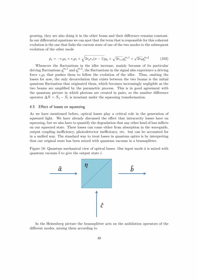
growing, they are also doing it in the other beam and their difference remains constant.In our differential equations we can spot that the term that is responsible for this coherentevolution is the one that links the current state of one of the two modes to the subsequentevolution of the other mode
ps = −rsps + rspi +√
2rprs(σ − 1)pp +√
2re,sqin,1s +
√2r0q
in,2s (102)
Whenever the fluctuations in the idler increase, mainly because of its particulardriving fluctuations qin,1i and qin,2i , the fluctuations in the signal also experience a drivingforce rspi that pushes them to follow the evolution of the idler. Thus, omiting thelosses for now, the only decorrelation that exists between the two beams is the initialquantum fluctuation that originated them, which becomes increasingly negligible as thetwo beams are amplified by the parametric process. This is in good agreement withthe quantum picture in which photons are created in pairs, so the number differenceoperator ∆N = Ns − Ni is invariant under the squeezing transformation.
4.5 Effect of losses on squeezing
As we have mentioned before, optical losses play a critical role in the generation ofsqueezed light. We have already discussed the effect that intracavity losses have onsqueezing, but we also have to quantify the degradation that any other kind of loss inflictson our squeezed state. These losses can come either from absorption in the waveguide,output coupling inefficiency, photodetector inefficiency, etc. but can be accounted forin a unified way. The standard way to treat losses in quantum optics is by interpretingthat our original state has been mixed with quantum vacuum in a beamsplitter.
Figure 18: Quantum mechanical view of optical losses. Our input mode a is mixed withquantum vacuum b to give the output state c.
In the Heisenberg picture the beamsplitter acts on the anihilation operators of thedifferent modes, mixing them according to
49

c = a√η + b
√1− η (103)
Which leads to the following mean and variance of the number of photons in theoutput mode
〈N〉 = 〈cc†〉 = ηN0 (104)
V ar(n) = 〈N2〉 − 〈N〉2 = η2V ar(N0) + η(1− η)〈N0〉 (105)
where N0 is the number operator for the input mode and N0 is its mean.Now, we are not so much interested in knowing about the variance of each indepen-
dent mode but rather about the variance of their difference. To that end, we will followthe approach of [3] and define the state of each mode after going through a hypotheticalbeam-splitter and then evaluate the variance of the difference, which will be of the form
V ar(Ns − Ni) = V ar(Ns) + V ar(Ni)− 2CoV ar(Ns, Ni) (106)
The two modes are transformed as
cs = as√ηs + bs
√1− ηs (107)
ci = ai√ηi + bi
√1− ηi (108)
So the covariance is calculated as
CoV ar(Ns, Ni) = 〈NsNi〉 −NsNi = ηsηiCoV ar(Ns,0, Ni,0) (109)
giving
V ar(Ns−Ni) = η2sV ar(Ns,0)+ηs(1−ηs)Ns,0+η2i V ar(Ni,0)+ηi(1−ηi)Ni,0−2ηsηiCoV ar(Ns,0, Ni,0)
(110)which in the case of equal losses reduces to
V ar(Ns − Ni) = η2V ar(Ns,0 − Ni,0) + η(1− η)(Ns,0 +Ni,0) (111)
Now, we notice that we can express the variance of the squeezed observable asV ar(Ns − Ni) = SV0 where V0 is the variance of a coherent beam of amplitude equal toNs +Ni. Therefore we can reduce the previous expression to
V ar(Ns − Ni) = (ηS + (1− η))ηV0 (112)
So the new squeezing factor is Sη + (1 − η) and ηV0 is the variance of a coherentbeam with amplitude equal to the sum of the current signal and idler modes.
50
4.6 Trade-off between squeezing and oscillation threshold
As we have previously seen, the amount of achievable squeezing depends greatly on theescape efficiency of the cavity, defined as the fraction of the generated photons that leavethe cavity without being absorbed or scattered. This can also be expressed as ζ = re
re+r0.
In order to preserve the quantum correlations among photons, these have to leave thecavity as fast as possible, in order to avoid being lost and thus break the pair-wisestructure of the state. Therefore, the first specification to take into account when wedesign a four-wave mixing source intended to produce squeezed light is to reduce theinternal losses as much as possible. This, in terms of resonator design, translates tohaving a resonator with a very high intrinsic quality factor, Q, which is a measure of theratio between the energy that is stored in the cavity and the power that is dissipatedbecause of the internal losses. It can also be expressed in terms of the linewidth of thecavity or, equivalently, in terms of the field decay rate.
Q0 = ω0U
Pd=
ω0
∆ωFWHM=
ω0
2r0(113)
When the internal losses are small, the intrinsic Q becomes large and thus the escapeefficiency increases. However, it is not possible to obtain a cavity with arbitrarily lowlosses, so a realistic solution is to fix a Q0 as high as we can and then overcouple thecavity so that the escape efficiency is still large.
The problem with overcoupling the cavity is that it also makes the oscillation thresh-old of the four-wave mixing process larger, so one has to pump with higher power inorder to obtain macroscopic beams for the signal and idler modes. Therefore, it is con-venient to understand the compromise between squeezing and oscillation threshold inorder to assess the feasibility of a design.
From the CMT equations of FWM that we have stated before we find the steadystate by solving the system
δAsδt
= −(rext,s + r0,s)As − jωβA2pA∗i = 0 (114)
δAiδt
= −(rext,i + r0,i)Ai − jωβA2pA∗s = 0 (115)
δApδt
= −(rext,p + r0,p)Ap − j2ωβA∗pAsAi − j√
2rext,pSp,+ = 0 (116)
This system has two solutions for the above and below threshold regimes. Abovethreshold (As 6= 0, Ai 6= 0) we find
|Ap|2 =
√rirsω2β2
(117)
|As|2 =
√r2pri
4ω2β2rs( 4
√4ω2β2r2e,pr2prsri
|Sp| − 1) (118)
51

|Ai|2 =
√r2prs
4ω2β2ri( 4
√4ω2β2r2e,pr2prsri
|Sp| − 1) (119)
where rk = re, k + r0 and we can see that solutions only exist for
|Sp|2 > Pth =r2prs
2re,pωβ(120)
The simplest case, and also the most common in on-chip resonators, is that allwavelengths are equally coupled to the ring. We would like to analyze how the couplinginfluences both the squeezing and the oscillation threshold, so we will set some reasonablevalues for the rest of the parameters in order to have an order of magnitude analysis.We will assume a ring with an internal Q of 500K, which we have demonstrated in oursilicon nitride process and a nonlinear refractive index of n2 = 2.4× 10⁻¹⁹, as measuredin silicon nitride. From [6] and [2] we can calculate our nonlinear constant β to be
β =3χ(3)
4n4nlε0Veff=
n2c
2n2nlVeff(121)
with nnl the refractive index of the nonlinear material and Veff given in the over-lap integral from [2]. A reasonable choice of dimensions for the ring gives a nonlinearparameter of approximately β = 5× 10⁴J−1. We can now find the oscillation thresholdand the squeezing factor for different couplings re and observe the tradeoff that existsbetween them.
Figure 19: Trade-off between squeezing at zero frequency and oscillation threshold.
We observe that there is a minimum for the oscillation threshold, for which theobtained squeezing would be around 2 dB. This is because we have assumed that thecoupling between the ring and the bus is the same for all modes, which is a good ap-proximation for a normal ring-bus coupler. Under these conditions, we can see that theoscillation threshold is a function that has a minimum for re = r0/2. Also, we see thatfor high squeezing factors we need to overcouple the ring so much that the oscillation
52

threshold becomes prohibitively large. This would not be a problem if light could becollected perfectly at the output of the ring, given that many quantum information ap-plications require only a degree of squeezing of 3 dB [4], which imposes more modestrestrictions on our oscillation threshold. However, to effectively calculate the degree ofsqueezing that we will be able to detect we have to take into account how the losses inthe waveguide and the output coupler will modify our initial squeezed state. We findthat when we take into consideration these losses, the required squeezing factor at theoutput of the ring needs to be of the order of 10 dB, which imposes serious restrictionson the oscillation threshold. If we name the initial squeezing factor S0 and the totallosses L (from the output coupler, detection inefficiency, etc.) we have
Figure 20: Pairs (S0, L) that give a final squeezing of 3 dB
For a total loss of 2.5 dB, which is an optimistic assumption if one takes into accounttypical grating coupler efficiencies, we need an initial squeezing of around 10 dB and thusour oscillation threshold shoots up above 1W of optical power in the bus waveguide,which is absolutely impractical. The first option to improve this situation is to havea better intrinsic Q, which would simultaneously enhance the squeezing and lower theoscillation threshold.
53
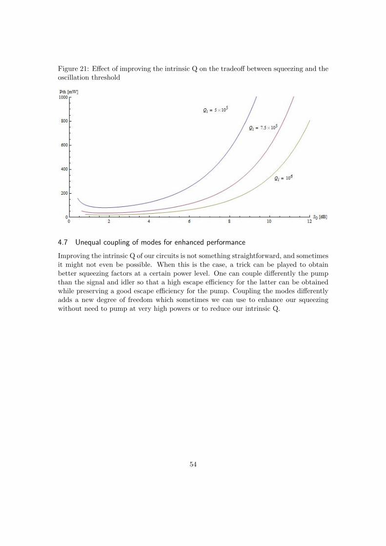
Figure 21: Effect of improving the intrinsic Q on the tradeoff between squeezing and theoscillation threshold
4.7 Unequal coupling of modes for enhanced performance
Improving the intrinsic Q of our circuits is not something straightforward, and sometimesit might not even be possible. When this is the case, a trick can be played to obtainbetter squeezing factors at a certain power level. One can couple differently the pumpthan the signal and idler so that a high escape efficiency for the latter can be obtainedwhile preserving a good escape efficiency for the pump. Coupling the modes differentlyadds a new degree of freedom which sometimes we can use to enhance our squeezingwithout need to pump at very high powers or to reduce our intrinsic Q.
54

Figure 22: Tradeoff between squeezing and oscillation threshold for different couplings.Here we suppose that re,s = re,i 6= re,p and also we have supposed an intrinsic qualityfactor of Qi = 500K. We observe that three operation regions exist: for low squeezingfactors it is benefitial to couple all the modes equally, given that it produces maximumfield enhancement. When we increase the required squeezing factor, equal and unequalstrategies become equivalent and, finally, if we need to obtain very high squeezing factors,the need to overcouple signal and idler makes it preferable to use unequal couplings.
4.8 Interferometric coupling
To obtain unequal coupling for different modes, a technique known as interferometriccoupling can be used [34]. This technique consists in coupling the ring and the buswaveguide in two points, such that a fraction of the light enters the resonator in thefirst coupler and another fraction does it in the second coupler. Then, two extremesituations can occur: the light that enters the ring in the second coupler can be in orout of phase with the light that is already resonating. If it is in phase, the fields willinterfere constructively and therefore the power transfer from the bus to the ring will beenhanced. If the light is totally out of phase, the fields will interfere destructively andless power transfer will occur.
55

Figure 23: Layout of a ring with interferometric coupling. Some light first enters throughthe lower coupler and resonates while the rest travels an extra lenght and gets into theresonator through the upper coupler.
The CMT model that describes this process is
d
dta = (jω0 − r′)a− jµ′is+ (122)
s− = −jµ′0a+Rs+ (123)
with
r′ = r1 + r2 +√
4r1r2ej(θ−φ) (124)
µ′i =√
2r1 +√
2r2ej(θ−φ) (125)
µ′0 = µ′ie−jφ = µ′∗i R (126)
Here we observe that, for equal couplings r1 = r2, light that interferes constructively(θ − φ = 0) gives rise to a total coupling coefficient of r′ = 4r1, which corresponds to apower transfer coefficient ρ′ = 2r′ = 8r1 = 4ρ1. This fourfold enhancement of the powercoupling coefficient is consistent with the fact that the fields add coherently, whereas inthe case of incoherent light the power transfer would have been enhanced by a twofoldfactor. On the other side, one can see that if light interferes destructively (θ − φ = π)there is no coupling to the ring.
We can now find the length that light has to travel between couplers, L, so thatthe high and low couplings occur in synchrony with the resonances of the ring. Thephase condition for constructive interference is θ − φ = 2πm, which supposing equalpropagation constants for the bus and ring and writing L = απR becomes
56
β(πR− L) = m2π (127)
β(1− α)πR = m2π (128)
neffk0 =1
1− α2m
R(129)
2πf0 =2c
(1− α)Rneffm (130)
f0 =c
(1− α)Rneffπm (131)
(132)
So we can appreciate that the periodicity of the coupling (which is produced by theMach-Zender structure) corresponds to FSRMZ = 2
1−αFSRring. For our application,we want the FSR of the MZ to be twice that of the ring, such that the coupling will bealternatively high and low, so L = 2πR.
If we want to make this calculation more accurate and take into account that thepropagation constant is not the same inside the ring as in the external arm, we come upwith the result FSRMZ = 2
AFSRring, where
A = 1−∫βbusdl
βringπR(133)
As we have mentioned, having equal coupling coefficients r1 = r2 causes the effectivecoupling to vary from totally constructive interference to totally destructive interference.An intermediate case, and in fact the case that we will be interested in, is to have slightlydifferent coupling coefficients r1 6= r2 such that the coupling when θ−φ = π is not exactlyzero but still low.
57
5 A classical application: coherence engineering
5.1 Motivation
In this section we want to investigate if one can use FWM to generate an idler beamthat has very narrow linewidth from a broader linewidth pump with better performancethan one could achieve by the traightforward strategy of filtering. The main intuition inthis work is that, if one designs a ring where the signal and idler have different couplingsand therefore different linewidth, the fluctuations in the pump are going to be absorbedassymetrically by the signal and idler, ideally providing a signal with much reducedfluctuations and a very noisy idler.
5.2 Numerical simulations of FWM
As a first approach to demonstrating the effect that we mentioned, we set up numericalsimulations of the FWM interaction between three frequency modes in a resonator, inorder to gain intuition about the nonlinear effects that arise. These simulations willbasically consist in numerically solving the system of coupled differential equations thatdescribe FWM. The advantage of using numerical simulations in first place is that theyallow us to introduce the randomness associated with incoherent light in our calcula-tions, whereas the standard analysis of FWM with CMT deals with pure monochromaticmodes. An analytical model of incoherent CMT would need to include stochastic differ-ential equations, which we have had to leave out of the scope of this project.
For a lossless FWM process we can find the following steady state conditions as aparticular case of the general expressions stated before
|Ap| = 4
√rirsω2β2
(134)
|As| =
√√√√ rp2ωβ
√rirs
(
√2ωβ
rp
14√rsri|Sp,+| − 1 (135)
|Ai| =
√√√√ rp2ωβ
√rsri
(
√2ωβ
rp
14√rsri|Sp,+| − 1 (136)
and the oscillation threshold
|Sp,+| = 4
√rsrir2p4ω2β2
(137)
Now, in order to run numerical simulations of the evolution of the CMT equations,we come up with a normalized version. We normalize them to the bandwidth of thepump resonance, so that the time scale of the evolution is in units of inverse bandwidth,which is approximately the coherence time. Also, we reescale the mode amplitudes.
58

δBsδτ
= −ρsBs − jB2pB∗i (138)
δBiδτ
= −ρiBi − jB2pB∗s (139)
δBpδτ
= −Bp − jB∗pBiBs − jTp,+ (140)
Ts,− = −j2√ρsBs (141)
Ti,− = −j2√ρiBi (142)
Tp,− = −j2Bs (143)
where we have defined τ = trp
, Bk = AkA0
and Tk,+ =Sk,+S0
, with
S0 =
√r2p
2ωβ(144)
A0 =
√rpωβ
(145)
Notice that S0 is the oscillation threshold in the case where all the couplings areequal and A0 is the pump saturation amplitude for that same case.
Now, from these CMT equations we can more easily find that the following conditionsfor the amplitudes have to be fulfilled in steady state
|Bp| = 4√ρsρi (146)
|Bi|2 =1
2( 4
√ρsρ3i|Tp,+| −
√ρsρi
) (147)
|Bs|2 =1
2( 4
√ρiρ3s|Tp,+| −
√ρiρs
) (148)
and for the phases
2φp − φs − φi =π
2(149)
φinp = φp +π
2(150)
Now we can test our code making sure that this predictions are retrievedFirst we make sure that the oscillation threshold for the equal coupling case is indeed
Tp,+ = 1
59

Figure 24: Energy of signal and idler inside the ring for different pumps
If we set all our coupling coefficients to be equal, the amplitudes in steady statereduce to
|Bs|2 = |Bi|2 =|Tp,+| − 1
2(151)
which we can check in our simulations.
60

Figure 25: Evolution of the energy of the modes inside the ring. The blue curvesrepresent the signal and idler energies (degenerate case) for pumps in the range Tp,+ =[0, 0.5, 1, 1.5, 2, 2.5, 3]
5.3 A model of incoherent light
Once our code is tested, we are interested in using it to evaluate the performance ofthe FWM mechanism when the coherent input is replaced with an incoherent one. Tothis end, our first task is to define a model for incoherent light that will be usefulin our calculations. In many cases, partially coherent light is produced when a largenumber of emitters radiate light at very similar frequencies but with small perturbationsthat cause differences amongst them. For instance, this is the case in gas lasers, whereeach atom has a different velocity which leads to a different Doppler shift. Moreover,even in the absence of any non-ideality, an emitter will always have a natural linewidthwhich is caused by the Heisenberg uncertainty relation between the time of emission ina quantum transition and the energy of that transition. Therefore, a valid model forour incoherent light is to write it as the sum of many monochromatic sources emittingat slightly different frequencies and with random phases. If we take the frequencies tobe distributed in a narrow interval ω0 ± ε/2 and with random phases, it can be shownthat this can be modelated with a source with constant intensity and phase jumps onthe timescale of 2π/ε [31]. This effectively tells us that the coherence time of the sourceof light is the inverse of the bandwidth of the signal.
The way we simulate this is by using an input signal with constant amplitude butwith randomly fluctuating phase. Our first model of the random fluctuations of the
61

phase is a signal with random jumps every coherence time of the pump, that is, everyτc = 1/rp
Figure 26: Model of the incoherent phase
A more complete description could set the time between phase shifts to be an expo-nential random variable with mean equal to the coherence time.
Figure 27: Model of the incoherent phase whith exponentially distributed time betweenshifts
Now if we run a simulation of the FWM process with incoherent pump phase (with
62
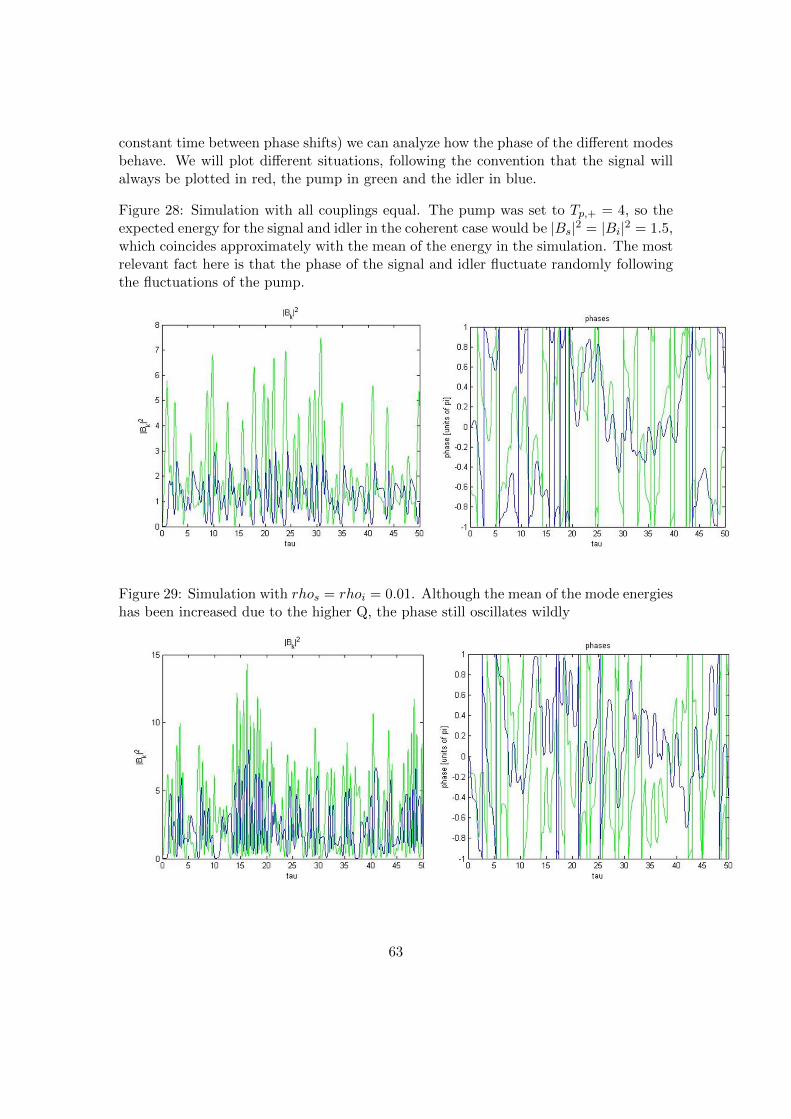
constant time between phase shifts) we can analyze how the phase of the different modesbehave. We will plot different situations, following the convention that the signal willalways be plotted in red, the pump in green and the idler in blue.
Figure 28: Simulation with all couplings equal. The pump was set to Tp,+ = 4, so theexpected energy for the signal and idler in the coherent case would be |Bs|2 = |Bi|2 = 1.5,which coincides approximately with the mean of the energy in the simulation. The mostrelevant fact here is that the phase of the signal and idler fluctuate randomly followingthe fluctuations of the pump.
Figure 29: Simulation with rhos = rhoi = 0.01. Although the mean of the mode energieshas been increased due to the higher Q, the phase still oscillates wildly
63
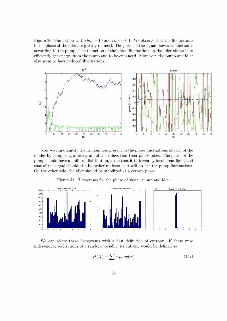
Figure 30: Simulation with rhos = 10 and rhoi = 0.1. We observe that the fluctuationsin the phase of the idler are greatly reduced. The phase of the signal, however, fluctuatesaccording to the pump. The reduction of the phase fluctuations in the idler allows it toefficiently get energy from the pump and to be enhanced. Moreover, the pump and idleralso seem to have reduced fluctuations.
Now we can quantify the randomness present in the phase fluctuations of each of themodes by computing a histogram of the values that their phase takes. The phase of thepump should have a uniform distribution, given that it is driven by incoherent light, andthat of the signal should also be rather uniform as it will absorb the pump fluctuations.On the other side, the idler should be stabilized at a certain phase.
Figure 31: Histograms for the phase of signal, pump and idler
We can relate these histograms with a first definition of entropy. If these wereindependent realizations of a random variable, its entropy would be defined as
H(X) =∑−pilog(pi) (152)
64
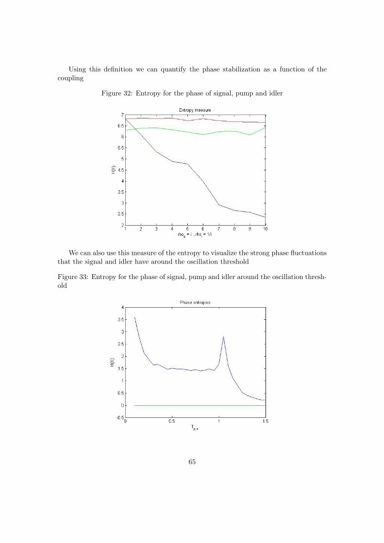
Using this definition we can quantify the phase stabilization as a function of thecoupling
Figure 32: Entropy for the phase of signal, pump and idler
We can also use this measure of the entropy to visualize the strong phase fluctuationsthat the signal and idler have around the oscillation threshold
Figure 33: Entropy for the phase of signal, pump and idler around the oscillation thresh-old
65
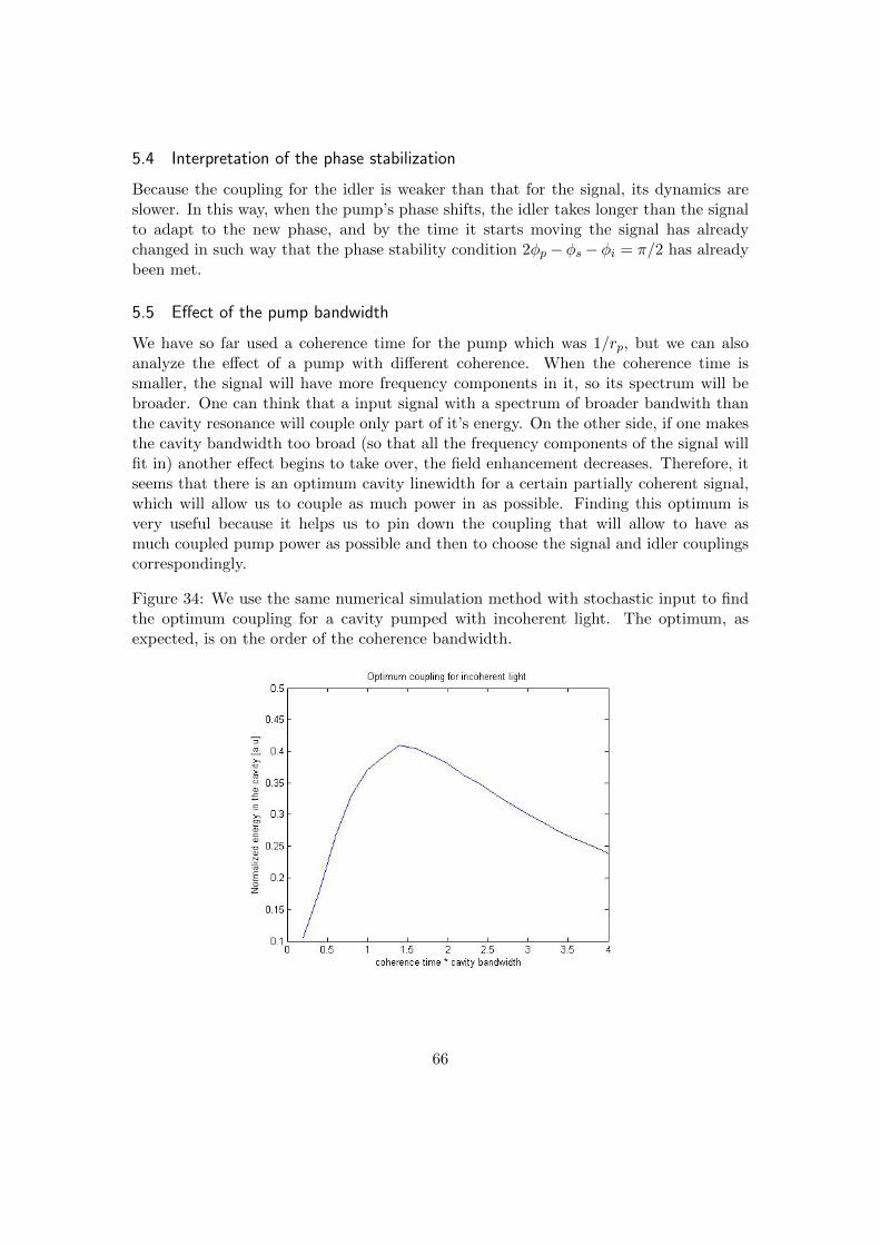
5.4 Interpretation of the phase stabilization
Because the coupling for the idler is weaker than that for the signal, its dynamics areslower. In this way, when the pump’s phase shifts, the idler takes longer than the signalto adapt to the new phase, and by the time it starts moving the signal has alreadychanged in such way that the phase stability condition 2φp − φs − φi = π/2 has alreadybeen met.
5.5 Effect of the pump bandwidth
We have so far used a coherence time for the pump which was 1/rp, but we can alsoanalyze the effect of a pump with different coherence. When the coherence time issmaller, the signal will have more frequency components in it, so its spectrum will bebroader. One can think that a input signal with a spectrum of broader bandwith thanthe cavity resonance will couple only part of it’s energy. On the other side, if one makesthe cavity bandwidth too broad (so that all the frequency components of the signal willfit in) another effect begins to take over, the field enhancement decreases. Therefore, itseems that there is an optimum cavity linewidth for a certain partially coherent signal,which will allow us to couple as much power in as possible. Finding this optimum isvery useful because it helps us to pin down the coupling that will allow to have asmuch coupled pump power as possible and then to choose the signal and idler couplingscorrespondingly.
Figure 34: We use the same numerical simulation method with stochastic input to findthe optimum coupling for a cavity pumped with incoherent light. The optimum, asexpected, is on the order of the coherence bandwidth.
66

5.6 Theoretical analysis: a phase restriction
One approach to analyze the FWM process with a broadband pump is to decompose it asa sum of single frequency modes and find the efficiency for each of them. However, thatraises a question: in the case when the pump is detuned from the center of the resonance,at what frequencies will the signal and idler appear? We know that in absence of detuningthe competition between the different modes is resolved by lasing at the center of eachresonance, which is the setting that has the greatest gain. However, when we detune thepump from the center of the resonance and add different couplings for signal and idlerthe situation is non-trivial. Here we derive a simple restriction between the frequency ofsignal and idler that, together with the energy conservation condition, allow us to findthe frequencies at which lasing will happen.
We state the CMT model for lossless FWM making the undepleted pump approxi-mation
δasδt
= −(jωs,0 + rs)as − jωsβa2pa∗i (153)
δai∗δt
= −(−jωi,0 + ri)a∗i + jωiβ(a∗p)
2as (154)
δapδt
= −(jωp,0 + rp)ap − j√
2rpsp,+ (155)
We define the envelopes such that ak = Ake−jωkt, where ωk is the frequency at which
the mode is actually oscillating. We assume that the pump mode Ap oscillates at thesame frequency as the pump input power Sp,+
δAsδt
= −(j(ωs,0 − ωs) + rs)As − jωsβA2pA∗i e−j(2ωp−ωs−ωi)t (156)
δAi∗δt
= −(−j(ωi,0 − ωi) + ri)A∗i + jωiβ(A∗p)
2Asej(2ωp−ωs−ωi)t (157)
δApδt
= −(j(ωp,0 − ωp) + rp)Ap − j√
2rpSp,+ (158)
We are going to assume that energy conservation is fulfilled, that is, that 2ωp−ωs−ωi = 0. From the steady state condition dAk
dt = 0 we find
A∗i =−jβωi(A∗p)2Asj(ωi,0 − ωi)− ri
(159)
which we can plug in (1) to find
(j(ωs,0 − ωs) + rs)As =−β2ωsωi|Ap|4Asj(ωi,0 − ωi)− ri
(160)
(j(ωs,0 − ωs) + rs)(j(ωi − ωi,0) + ri) = β2ωsωi|ap|4 (161)
67

(ωs − ωs,0)(ωi − ωi,0) + j(ri(ωs,0 − ωs) + rs(ωi − ωi,0) + rsri = β2ωsωi|ap|4 (162)
we realize that the imaginary part of the left hand term has to be equal to zero
ri(ωs,0 − ωs) = rs(ωi,0 − ωi) (163)
Which means that both signal and idler have to be detuned equally from resonance,in units of the resonance bandwidth. A way to interpret this is to see that the phaseshift introduced by the resonator has to be the same in both modes.
Now we can join this with the energy conservation relation 2ωp − ωs − ωi = 0 andfind that, in the case where the resonances are energy matched (2ωp,0 − ωs,0 − ωi,0 = 0) the detunings from resonance fulfil
∆ωs =2∆ωp
1 + ri/rs(164)
∆ωi =2∆ωp
1 + rs/ri(165)
Figure 35: In simulations we set three energy matched resonances and detune the inputpump from the middle peak. We observe that signal and idler are detuned according toour predictions.
68

5.7 Implementation
To demonstrate this concept we can use a superluminiscent LED (SLED), which normalyhave a linewidth of some tens of nanometers. To convert this linewidth to bandwidthwe can use the relation
∆λ =λ20c
∆f (166)
Now, a comercially available SLED can have a linewidth of some 30 nm, whichtranslates to ∆f ≈ 1012. On the other side, a cavity where we expect to produce FWMcannot have a Q below some hundred thousands, which corresponds to ∆f ≈ 109. If wepump our cavity with such source, we are efectively limiting the amount of light thatwill be able to couple to the ring, and thus our parametric process will require higherinput powers in order to get started. However, even if this is the case, the cavity wouldonly act as a filter for the pump power and for a high enough input power oscillationshould still be visible.
69
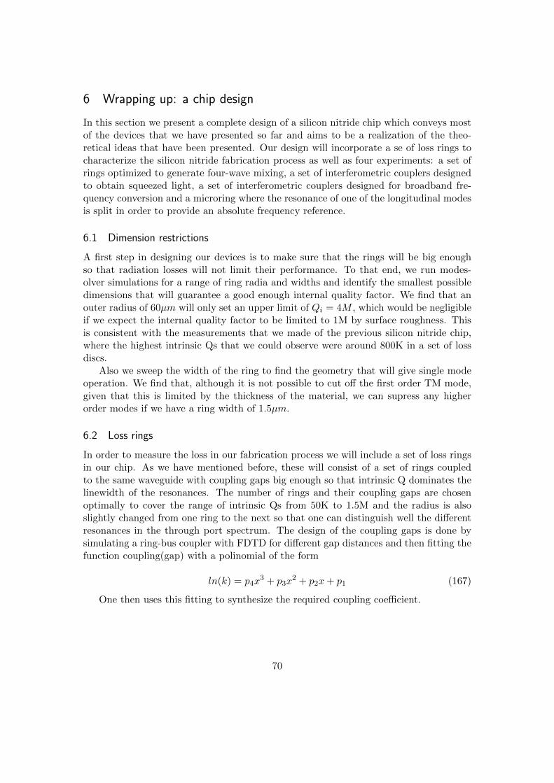
6 Wrapping up: a chip design
In this section we present a complete design of a silicon nitride chip which conveys mostof the devices that we have presented so far and aims to be a realization of the theo-retical ideas that have been presented. Our design will incorporate a se of loss rings tocharacterize the silicon nitride fabrication process as well as four experiments: a set ofrings optimized to generate four-wave mixing, a set of interferometric couplers designedto obtain squeezed light, a set of interferometric couplers designed for broadband fre-quency conversion and a microring where the resonance of one of the longitudinal modesis split in order to provide an absolute frequency reference.
6.1 Dimension restrictions
A first step in designing our devices is to make sure that the rings will be big enoughso that radiation losses will not limit their performance. To that end, we run modes-olver simulations for a range of ring radia and widths and identify the smallest possibledimensions that will guarantee a good enough internal quality factor. We find that anouter radius of 60µm will only set an upper limit of Qi = 4M , which would be negligibleif we expect the internal quality factor to be limited to 1M by surface roughness. Thisis consistent with the measurements that we made of the previous silicon nitride chip,where the highest intrinsic Qs that we could observe were around 800K in a set of lossdiscs.
Also we sweep the width of the ring to find the geometry that will give single modeoperation. We find that, although it is not possible to cut off the first order TM mode,given that this is limited by the thickness of the material, we can supress any higherorder modes if we have a ring width of 1.5µm.
6.2 Loss rings
In order to measure the loss in our fabrication process we will include a set of loss ringsin our chip. As we have mentioned before, these will consist of a set of rings coupledto the same waveguide with coupling gaps big enough so that intrinsic Q dominates thelinewidth of the resonances. The number of rings and their coupling gaps are chosenoptimally to cover the range of intrinsic Qs from 50K to 1.5M and the radius is alsoslightly changed from one ring to the next so that one can distinguish well the differentresonances in the through port spectrum. The design of the coupling gaps is done bysimulating a ring-bus coupler with FDTD for different gap distances and then fitting thefunction coupling(gap) with a polinomial of the form
ln(k) = p4x3 + p3x
2 + p2x+ p1 (167)
One then uses this fitting to synthesize the required coupling coefficient.
70
Figure 36: Layout of the loss ring set
6.3 Four wave mixing rings
As we have mentioned, our ultimate goal is to produce two-mode squeezed light, whichrequires to generate parametric oscillation with overcoupled signal and idler. However,as an intermediate step, we also include a set of rings that are designed to achieveparametric oscillation without the overcoupling required to have squeezing.Here we alsoshow that a single ring does not allow one to generate squeezed light at a reasonablepower level, and justify the need to use interferometric coupling.
6.3.1 Dispersion
The first consideration we have to make is that our rings be dispersionless, or at leastthat they have small enough dispersion to allow FWM to occur. To assess this we usethe method described in [35] to find ∆FSR, that is, the mismatch between two adjacentFSRs which is responsible for the energy mismatch in FWM. We calculate this parameterfor different geometries of the ring (sweeping its radius and its width) and realize thatthe dispersion of our design is very insensitive to these variations. This occurs becauseof the large dimensions of our ring and the low index contrast, which makes the modeprofile rather stable against perturbations of the ring. Nevertheless, we also realize thatthe dispersion of our ring is small enough so that we do not require to do much dispersionengineering. A practical rule of thumb is that if our resonances are wide enough, with aHFHM of about two or three times ∆FSR, dispersion will not hinder the occurrence ofFWM. We find ∆FSR to be in the order of 0.2 GHz, which means that our resonancesshould have a bandwidth of about 1 GHz.
6.3.2 Critically coupled rings
As we know from [2], the most efficient way to generate parametric oscillation in a singlering is by critically coupling it. Although this does not provide squeezing, it is a goodstep towards demonstrating nonlinear optics in silicon nitride, and therefore it would bean interesting experiment to do. Considering an intrinsic Q of 500K, as we demonstrated
71
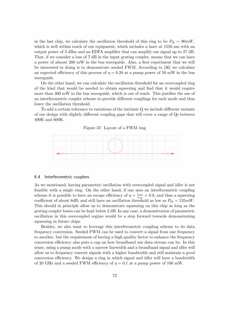
in the last chip, we calculate the oscillation threshold of this ring to be Pth = 90mW ,which is well within reach of our equipment, which includes a laser at 1550 nm with anoutput power of 3 dBm and an EDFA amplifier that can amplify our signal up to 27 dB.That, if we consider a loss of 7 dB in the input grating coupler, means that we can havea power of almost 200 mW in the bus waveguide. Also, a first experiment that we willbe interested in doing is to demonstrate seeded FWM. According to [36] we calculatean expected efficiency of this process of η = 0.28 at a pump power of 50 mW in the buswaveguide.
On the other hand, we can calculate the oscillation threshold for an overcoupled ringof the kind that would be needed to obtain squeezing and find that it would requiremore than 300 mW in the bus waveguide, which is out of reach. This justifies the use ofan interferometric coupler scheme to provide different couplings for each mode and thuslower the oscillation threshold.
To add a certain tolerance to variations of the intrinsic Q we include different variantsof our design with slightly different coupling gaps that will cover a range of Qs between400K and 600K.
Figure 37: Layout of a FWM ring
6.4 Interferometric couplers
As we mentioned, having parametric oscillation with overcoupled signal and idler is notfeasible with a single ring. On the other hand, if one uses an interferometric couplingscheme it is possible to have an escape efficiency of η = rext
rtot= 0.8, and thus a squeezing
coefficient of about 8dB, and still have an oscillation threshold as low as Pth = 135mW .This should in principle allow us to demonstrate squeezing on this chip as long as thegrating coupler losses can be kept below 2 dB. In any case, a demonstration of parametricoscillation in this overcoupled regime would be a step forward towards demonstratingsqueezing in future chips.
Besides, we also want to leverage this interferometric coupling scheme to do datafrequency conversion. Seeded FWM can be used to convert a signal from one frequencyto another, but the requirement of having a high quality factor to enhance the frequencyconversion efficiency also puts a cap on how broadband our data stream can be. In thissense, using a pump mode with a narrow linewidth and a broadband signal and idler willallow us to frequency convert signals with a higher bandwidth and still maintain a goodconversion efficiency. We design a ring in which signal and idler will have a bandwidthof 20 GHz and a seeded FWM efficiency of η = 0.1 at a pump power of 100 mW.
72

To add tolerance to missalignments between the resonances and the frequency de-pendent couplings, we include different variants of the design with slightly different pathdifferences between the two couplers.
6.5 Absolute frequency reference
We finally include a design of a ring with a modulation of the outer wall of the kindthat we have presented as a way to have an absolute frequency reference. To determinethe amplitude of the modulation of the outer wall we use the approximation that theresonance splitting induced by a sinusoidal modulation of the wall will be approximatelythe same as the resonance shift induced by an offset of the wall of the same amplitude.Therefore, with the help of simulations, we establish that a modulation of the wall ofjust 5 nm will suffice to create a splitting of about 5 GHz, which will be fully identifiabledespite the linewidth of the resonances. Also, one has to choose well the longitudinalmode that will be splitted, in order that the doublet appears at a wavelength which wecan observe well. To create the doublet at 1550 nm, we find that one has to split themode 368 of the resonator, which means that the sinusoidal modulation has to have 736periods around the ring. This means that the length of a semiperiod is around 250 nm,which is fully resolvable by electron beam lithography.
Figure 38: Layout of the absolute frequency reference device with a close-up to themodulation of the outer wall
73

Figure 39: Layout of the complete chip

References
[1] C.Fabre, Noise characteristics of a non-degenerate Optical Parametric Oscillator -Application to quantum noise reduction. J.Phys. France 50 (1989) 1209-1225
[2] X.Zeng, Design of triply-resonant microphotonic parametric oscillators based onKerr nonlinearity. Optics Express, Vol. 22, Issue 13, pp. 15837-15867 (2014)
[3] M. Jasperse, Relative intensity squeezing by four-wave mixing in rubidium. PhDThesis at University of Melbourne
[4] S. Braunstein, P. van Loock, Quantum information with continuous variables. Re-views of Modern Physics, Vol 77, April 2005
[5] J. S. Levy, Integrated nonlinear optics in silicon nitride waveguides and resonators.PhD Thesis at Cornell University
[6] R.W. Boyd, Nonlinear Optics. Academic Press, Third edition, 2008.
[7] M.S. Wartak, Computational photonics, an introduction with Matlab. CambridgeUniversity Press, 2013.
[8] A. Yariv, Universal relations for coupling of optical power between microresonatorsand dielectric waveguides. Electronic Letters, Vol. 36 No .4
[9] H. A. Haus. Waves and Fields in Optoelectronics. Prentice-Hall, Englewood Cliffs,NJ, 1984.
[10] M. Lipson, A. Gaeta et al. , Tailored anomalous group-velocity dispersion in siliconchannel waveguides. Optics Express, Vol. 14 No.10
[11] Q.Lin, O. Painter, G.P. Agrawal, Nonlinear optical phenomena in silicon waveg-uides: modelling and application. Optics Express, Vol.15, No.25
[12] Y. Liu et al., Nonlinear optical properties of silicon waveguides. SemiconductorScience and Technology, Vol.23, No. 6 (2008)
[13] A. Bristow et al., Two-photon absorption and Kerr coefficients of silicon for 850-2200 nm. Applied Physics Letters 90, 191104 (2007)
[14] H. R. Philipp. Optical properties of silicon nitride. J. Electrochim. Soc. 120, 295-300(1973)
[15] S.C. Mao et al, Low propagation loss SiN optical waveguide prepared by optimallow-hydrogen module. Optics Express, Vol. 16 No. 25
[16] K. Luke et al. , Overcoming Si3N4 film stress limitations for high quality factor ringresonators . Optics Express, Vol. 21, No. 19
75
[17] Mark Wade, Designing rings for propagation loss measurement. Not published
[18] E. S. Hosseini et al, High quality planar silicon nitride microdisk resonators forintegrated photonics in the visible wavelength range. Optics Express, Vol.17, No. 17
[19] A. Gondarenko et al, High confinement micron-scale silicon nitride high Q ringresonator. Optics Express, Vol. 17, No. 14
[20] D.F. Walls and G. J. Milburn, Quantum Optics. Springer, second edition (2008)
[21] M.O. Scully and M.S. Zubairy, Quantum Optics. Cambridge University Press, firstedition (1997)
[22] C. Cohen-Tannoudji, Photons and atoms. Wiley-VCH, first edition (1997)
[23] S.L. Braunstein, P. van Loock, Quantum information with continuous variables.Reviews of modern physics, Vol. 77 No. 2
[24] H. A. Haus, Electromagnetic noise and quantum optical measurements. Springer-Verlag, first edition (2000)
[25] M. W. Mitchell , Quantum optics for the impatient. Class notes
[26] A.Predojevic, Rubidium resonant squeezed light from a diode-pumped optical-parametric oscillator. PhD thesis at ICFO and UPC
[27] S. Ast et al, High-bandwidth squeezed light at 1550 nm from a compact monolithicPPKTP cavity. Optics Express, Vol.21, No. 11 (2013)
[28] E.Pomarico et al, Engineering integrated pure narrow-band photon sources. NewJournal of Physics, 14 (2012) 033008
[29] H. Yonezawa et al, Generation of squeezed light with a monolithic optical parametricoscillator: Simultaneous achievment of phase matching and cavity resonance bytemperature control. Optics Express, Vol.18, No.19
[30] A. Einstein, B. Podolsky, N. Rosen, Can quantum-mechanical description of physicalreality be considered complete?. Physical Review, Vol. 47, pg. 777
[31] A. Lipson, S.G. Lipson, H. Lipson, Optical physics. Cambridge University Press,4th edition
[32] J.D. Joannopoulos, S.G. Johnson, J.N. Winn, R.D. Meade, Photonic crystals: Mold-ing the flow of light. Princeton University Press, 2nd edition, 2007
[33] S.G. Johnson et al, Perturbation theory for Maxwell’s equations with shifting bound-aries. Physical Review E, Volume 65, 066611
[34] M. Popovic, Theory and design of high index contrast microphotonic circuits. PhDThesis, Massachusetts Institute of Technology, EECS department.
76

[35] C. Gentry et al. , A discrete resonance, all-order dispersion engineering method formicrocavity design for four wave mixing. Conference paper, Frontiers in Optics 2014
[36] P.P. Absil et al., Wavelength conversion in GaAs micro-ring resonators. OpticsLetters, Vol 25, No 8
[37] H.A. Haus, et al. , Coupled-Mode Theory of optical waveguides. Journal of lightwavetechnology, vol LT-5, no1 (1987)
[38] S.J. Freedman, J.F. Clauser, Experimental test of local hidden-variable theories.Phys. Rev. Lett. 28 (938), (1972)
[39] A. Aspect, P. Grangier, G. Roger, Experimental tests of realistic local theories viaBell’s theorem. Phys. Rev. Lett. 47 (7) , (1981)
[40] C. Fabre et al. , Squeezing in detuned degenerate optical parametric oscillators.Quantum Optics, 2, 2
[41] R.E. Slusher et al. , Observation of squeezed states generated by four-wave mixingin an optical cavity. Phys. Rev. Lett, 55, 2409 (1985)
[42] R. Gosh, C.K. Hong, Z.Y. Ou, L. Mandel, Interference of two photons in parametricdown conversion. Phys. Rev. A 34, 3962 (1986)
[43] E. Knill, R. Laflamme, G.J. Milburn, A scheme for efficient quantum computationwith linear optics. Nature 409, 46-52
[44] R.Raussendorf, Measurement-based quantum computation with cluster states. Phys.Rev. A 68, 022312
[45] R.Ursin et al., Entanglement-based quantum communication over 144 km. NaturePhysics, 3, 481
[46] G.B. Lemos, Quantum imaging with undetected photons Nature 512 , 409-412
77