
Citation: Veledar, Omar (2007) Development of nanosecond...
156
Citation: Veledar, Omar (2007) Development of nanosecond range light sources for calibration of astroparticle cherenkov detectors. Doctoral thesis, Northumbria University. This version was downloaded from Northumbria Research Link: http://nrl.northumbria.ac.uk/3826/ Northumbria University has developed Northumbria Research Link (NRL) to enable users to access the University’s research output. Copyright © and moral rights for items on NRL are retained by the individual author(s) and/or other copyright owners. Single copies of full items can be reproduced, displayed or performed, and given to third parties in any format or medium for personal research or study, educational, or not-for-profit purposes without prior permission or charge, provided the authors, title and full bibliographic details are given, as well as a hyperlink and/or URL to the original metadata page. The content must not be changed in any way. Full items must not be sold commercially in any format or medium without formal permission of the copyright holder. The full policy is available online: http://nrl.northumbria.ac.uk/policies.html
Transcript of Citation: Veledar, Omar (2007) Development of nanosecond...

Citation: Veledar, Omar (2007) Development of nanosecond range light sources for calibration of astroparticle cherenkov detectors. Doctoral thesis, Northumbria University.
This version was downloaded from Northumbria Research Link: http://nrl.northumbria.ac.uk/3826/
Northumbria University has developed Northumbria Research Link (NRL) to enable users to access the University’s research output. Copyright © and moral rights for items on NRL are retained by the individual author(s) and/or other copyright owners. Single copies of full items can be reproduced, displayed or performed, and given to third parties in any format or medium for personal research or study, educational, or not-for-profit purposes without prior permission or charge, provided the authors, title and full bibliographic details are given, as well as a hyperlink and/or URL to the original metadata page. The content must not be changed in any way. Full items must not be sold commercially in any format or medium without formal permission of the copyright holder. The full policy is available online: http://nrl.northumbria.ac.uk/policies.html

Development of Nanosecond Range Light
Sources for Calibration of Astroparticle
Cherenkov Detectors
Omar Veledar
PhD
2007

Development of Nanosecond Range Light
Sources for Calibration of Astroparticle
Cherenkov Detectors
Omar Veledar
The thesis is submitted in partial fulfilment of the requirements
for the award of Doctor of Philosophy
University of Northumbria at NewcastleSchool of Computing, Engineering and Information Sciences
May 2007

Abstract
In this thesis the development of light emitting diodes (LED) is reviewed. The em-
phasis is put on devices emitting at the blue region of the spectrum. The physical
characteristics of these devices are considered. The main interest is based around the
ability of blue LEDs to generate nanosecond range optical flashes.
The fast pulsing electronic circuits capable of driving the devices are also reviewed.
These are complemented by the potentially exploitable techniques that could provide
further benefits for required fast optical pulse generation.
The simple, compact and inexpensive electronic oscillator for producing nanosecond
range pulses is developed. The circuitry is adapted for generation of pulses necessary
to switch on and assist with the turn off of blue InGaN based LEDs. The resulting
nanosecond range blue optical pulses are suitable for, but not limited to, the calibration
of scintillation counters. These devices used in neutrino detection experiments could
provide a better understanding of cosmology and particle physics.

Contents
List of Symbols v
List of Acronyms viii
Acknowledgements ix
Author’s Declaration x
Publications as a Result of Work on this Thesis xi
1 Introduction 1
1.1 Current State of the Art . . . . . . . . . . . . . . . . . . . . . . . . . . 3
1.2 Present Applications . . . . . . . . . . . . . . . . . . . . . . . . . . . . 3
1.3 Objectives . . . . . . . . . . . . . . . . . . . . . . . . . . . . . . . . . . 5
1.4 Scope of the Thesis . . . . . . . . . . . . . . . . . . . . . . . . . . . . . 6
1.5 Contributions . . . . . . . . . . . . . . . . . . . . . . . . . . . . . . . . 6
1.6 Thesis Structure . . . . . . . . . . . . . . . . . . . . . . . . . . . . . . . 6
2 The Light Emitting Diode 8
2.1 LED Development . . . . . . . . . . . . . . . . . . . . . . . . . . . . . 8
2.1.1 Present devices . . . . . . . . . . . . . . . . . . . . . . . . . . . 9
2.1.2 Future Devices . . . . . . . . . . . . . . . . . . . . . . . . . . . 16
2.2 LED Characteristics . . . . . . . . . . . . . . . . . . . . . . . . . . . . 18
2.2.1 Charge Properties . . . . . . . . . . . . . . . . . . . . . . . . . . 18
2.2.2 The P-N Junction . . . . . . . . . . . . . . . . . . . . . . . . . . 20
2.2.3 Electrical Properties . . . . . . . . . . . . . . . . . . . . . . . . 23
2.2.4 Optical Properties . . . . . . . . . . . . . . . . . . . . . . . . . 28
2.3 Advanced Structures - High Brightness LEDs . . . . . . . . . . . . . . 29
2.3.1 Single Heterojunction . . . . . . . . . . . . . . . . . . . . . . . . 30
2.3.2 Double Heterojunction . . . . . . . . . . . . . . . . . . . . . . . 31
2.3.3 Single Quantum Well - InGaN Based LEDs . . . . . . . . . . . 31
2.3.4 Manufacture of High Brightness LEDs . . . . . . . . . . . . . . 33
i
2.4 Applications . . . . . . . . . . . . . . . . . . . . . . . . . . . . . . . . . 35
2.5 Chapter 2 Summary . . . . . . . . . . . . . . . . . . . . . . . . . . . . 37
3 Pulse Shaping Techniques and LED Pulse Response 38
3.1 Types of LED Drivers . . . . . . . . . . . . . . . . . . . . . . . . . . . 38
3.1.1 Multivibrators . . . . . . . . . . . . . . . . . . . . . . . . . . . . 39
3.1.2 Emitter Coupled Monostable . . . . . . . . . . . . . . . . . . . 39
3.1.3 Avalanche Transistors . . . . . . . . . . . . . . . . . . . . . . . 40
3.1.4 Complementary Transistor Pair Regenerative
Switch . . . . . . . . . . . . . . . . . . . . . . . . . . . . . . . 41
3.1.5 Standard Telecommunication Techniques . . . . . . . . . . . . . 42
3.2 Overview of Standard Pulse Shaping
Techniques . . . . . . . . . . . . . . . . . . . . . . . . . . . . . . . . . 42
3.2.1 Differentiation . . . . . . . . . . . . . . . . . . . . . . . . . . . . 42
3.2.2 Step Recovery Diode . . . . . . . . . . . . . . . . . . . . . . . . 43
3.2.3 Clipping and High Speed Comparators . . . . . . . . . . . . . . 43
3.2.4 Non-Saturating Switch . . . . . . . . . . . . . . . . . . . . . . . 44
3.2.5 Speed up Commutating Capacitor for Transistor Switching . . . 45
3.2.6 Shorted Turn - Theory and Application . . . . . . . . . . . . . 46
3.3 LED Switching Parameters . . . . . . . . . . . . . . . . . . . . . . . . 50
3.4 Basic Switching Principles . . . . . . . . . . . . . . . . . . . . . . . . . 52
3.5 Chapter 3 Summary . . . . . . . . . . . . . . . . . . . . . . . . . . . . 53
4 LED Modelling 54
4.1 OrCAD Models . . . . . . . . . . . . . . . . . . . . . . . . . . . . . . . 55
4.1.1 Ideal Diode Static Model . . . . . . . . . . . . . . . . . . . . . . 55
4.1.2 Real Diode Static Model . . . . . . . . . . . . . . . . . . . . . . 56
4.1.3 Large Signal Model . . . . . . . . . . . . . . . . . . . . . . . . . 59
4.2 Behavioural Models . . . . . . . . . . . . . . . . . . . . . . . . . . . . . 60
4.3 Chapter 4 Summary . . . . . . . . . . . . . . . . . . . . . . . . . . . . 61
5 Experimental and Modelled LED Characteristics 62
5.1 Methods and Results . . . . . . . . . . . . . . . . . . . . . . . . . . . . 62
5.1.1 Capacitance - Voltage Relationship . . . . . . . . . . . . . . . . 63
5.1.2 Current - voltage relationship . . . . . . . . . . . . . . . . . . . 71
5.1.3 LED Output Spectrum . . . . . . . . . . . . . . . . . . . . . . 73
5.1.4 Current - Output Light Intensity Relationship . . . . . . . . . . 74
5.1.5 LED as a Photodetector . . . . . . . . . . . . . . . . . . . . . . 75
5.1.6 Correlation . . . . . . . . . . . . . . . . . . . . . . . . . . . . . 77
5.2 Modelling Results . . . . . . . . . . . . . . . . . . . . . . . . . . . . . 81
ii

5.2.1 OrCAD Model Editor . . . . . . . . . . . . . . . . . . . . . . . 81
5.2.2 OrCAD Behavioural Model . . . . . . . . . . . . . . . . . . . . 82
5.2.3 MATLAB Behavioural Model . . . . . . . . . . . . . . . . . . . 84
5.2.4 Model Comparison . . . . . . . . . . . . . . . . . . . . . . . . . 84
5.3 Chapter 5 Summary . . . . . . . . . . . . . . . . . . . . . . . . . . . . 86
6 Optical Pulse Generation 88
6.1 Investigation of the Current Arrangement . . . . . . . . . . . . . . . . 88
6.2 Totem-Pole Drivers . . . . . . . . . . . . . . . . . . . . . . . . . . . . 90
6.3 Single Output Configurations . . . . . . . . . . . . . . . . . . . . . . . 92
6.3.1 Switching Configuration . . . . . . . . . . . . . . . . . . . . . . 92
6.3.2 Pulse Shaping . . . . . . . . . . . . . . . . . . . . . . . . . . . . 93
6.3.3 Measurement Technique . . . . . . . . . . . . . . . . . . . . . . 95
6.3.4 Results and Discussion . . . . . . . . . . . . . . . . . . . . . . . 96
6.3.5 Error Treatment . . . . . . . . . . . . . . . . . . . . . . . . . . 99
6.4 Multiple Output Configuration . . . . . . . . . . . . . . . . . . . . . . 100
6.4.1 Circuit Arrangement . . . . . . . . . . . . . . . . . . . . . . . . 101
6.5 Chapter 6 Summary . . . . . . . . . . . . . . . . . . . . . . . . . . . . 104
7 Conclusions and Recommendations for Further Work 105
7.1 Conclusions . . . . . . . . . . . . . . . . . . . . . . . . . . . . . . . . . 105
7.2 Further Work . . . . . . . . . . . . . . . . . . . . . . . . . . . . . . . . 106
A Practical Diode Equation Analysis 108
A.1 Analysis by inspection . . . . . . . . . . . . . . . . . . . . . . . . . . . 108
A.2 Mathematical Analysis . . . . . . . . . . . . . . . . . . . . . . . . . . . 109
A.2.1 Manual Solution . . . . . . . . . . . . . . . . . . . . . . . . . . 110
B SPICE Diode Model Parameters 113
C LED Capacitance Analysis 115
C.1 Inverse Capacitance Squared Versus Voltage Plots . . . . . . . . . . . . 115
C.2 Depletion Capacitance Fit . . . . . . . . . . . . . . . . . . . . . . . . . 115
C.3 Diffusion Capacitance Fit . . . . . . . . . . . . . . . . . . . . . . . . . 116
C.4 Hump Capacitance Fit . . . . . . . . . . . . . . . . . . . . . . . . . . . 117
C.5 Fitting Errors . . . . . . . . . . . . . . . . . . . . . . . . . . . . . . . . 118
D LED Current - Voltage Analysis 122
E LED Output Spectrum Analysis 125
F LED Intensity Analysis 126
iii

G Using LED as a Photodetector 127
H Blue LED Model Netlist - Using OrCAD Model Editor 130
iv

List of Symbols
The following is a list of symbols used in the thesis:
Symbol Unit DescriptionA m2 cross sectional areaAc m2 core areaB T Magnetic Flux DensityBV V breakdown voltageCD F diode capacitanceCd F diffusion or injection capacitanceCj F junction or depletion capacitanceDn/p m2s−1 diffusion coefficientsEc1,2,3... eV energy of conduction band levelEg(well) eV well material energy band gapEgQW eV Quantum well energy band gapEv1,2,3... eV energy of valance band levelf Hz frequencyFWHM(observed) s measured FWHMFWHM(optical) s optical signal FWHMFWHM(system) s measuring system FWHMh Js Planck’s constant (6.6260755× 10⁻³⁴Js)H Am−1 Magnetic Field StrengthI or i A currentI(r,g) A generation-recombination currentID(ideal) A ideal diode currentIn A electron currentIs A saturation currentJCOND Am−2 sum of all drift and diffusion current densitiesJdiff Am−2 diffusion current densityJdrift Am−2 drift current densityJn Am−2 electron current densityJn(diff) Am−2 electron diffusion current densityJn(drift) Am−2 electron drift current densityJp Am−2 hole current densityJp(diff) Am−2 hole diffusion current densityJp(drift) Am−2 hole drift current densityJs Am−2 saturation current densityk NmK−1 Boltzmann’s constant (1.3806568× 10⁻²³JK−1)l m carrier mean free path
v

Symbol Unit Descriptionlc m core mean lengthlQW m quantum well lengthL H inductanceL0 H inductance in a coil with an air coreLn m electron minority carrier diffusion lengthLp m hole minority carrier diffusion lengthm∗
e kg electron effective massm∗
h kg hole effective massm∗
r kg reduced effective massn m−3 electron concentrationni m−3 intrinsic carrier concentrationnn0 m−3 majority electron carrier equilibrium concentrationnp m−3 minority electron carrier concentrationnp0 m−3 minority electron carrier equilibrium concentrationN number of coil turnsNA m−3 acceptor impurity concentrationNB m−3 impurity concentration of the lightly doped sideND m−3 donor impurity concentrationp m−3 hole concentrationpn m−3 minority hole carrier concentrationpn0 m−3 minority hole carrier equilibrium concentrationpp0 m−3 majority hole carrier equilibrium concentrationq C Electron charge (1.60217733 × 10⁻¹⁹C)Q C chargeQd C diffusion charge - due to minority carrier injectionQD C charge stored by a diodeQj C depletion charge - due to doping atoms concentrationQn C stored (electron) charge per unit areaQp C stored (hole) charge per unit areaR rate of direct recombination (radiation efficiency)R(f) LED frequency responseRp Ω diode parallel resistanceRs Ω diode series resistancet s timetfall s fall timetrise s rise timeT K Temperaturevbi V built in voltagevi ms−1 electron individual drift velocityvn ms−1 average electron drift velocityvp ms−1 average hole drift velocityvth ms−1 carrier thermal velocityV V VoltageVBE V transistor base-emitter voltageVEB V transistor emitter-base voltageVt V diode thermal voltageW m depletion layer width
vi

Symbol Unit Descriptionx m distance from the junctionxn m distance from the junction into n sidexp m distance from the junction into p sideβ m3s−1 radiation constant of proportionalityε NC−1 electric fieldǫS Fm−1 semiconductor dielectric permittivityη ideality factor or emission coefficientµ0 Hm−1 permeability in free spaceµn m2(V s)−1 electron mobilityµp m2(V s)−1 hole mobilityµr Hm−1 relative permeabilityν Hz frequency of lightξ V emfτc s mean free time (minority carrier lifetime)τf(PMT ) s PMT fall timeτf(scope) s oscilloscope fall timeτf(system) s measuring system fall timeτn s excess minority electron carriers’ lifetimeτp s excess minority hole carriers’ lifetimeτr(PMT ) s PMT rise timeτr(scope) s oscilloscope rise timeτr(system) s measuring system rise timeφ Wb magnetic flux
The additional symbols used for the SPICE diode model parameters are shown in
appendix B.
vii

List of Acronyms
The following is a list of acronyms used in the thesis:
Acronym MeaningAC Alternating CurrentANTARES Astronomy with a Neutrino Telescope and
Abyss environmental RESearchDC Direct CurrentDH Double HeterojunctionDUT Device Under TestDVM Digital Volt-MeterECL Emitter-Coupled LogicELOG Epitaxially Laterally OvergrownFWHM Full Width Half MaximumEMF Electro-Magnetic ForceHVPE Hybrid Vapour Phase EpitaxyIR InfraredLAN Local Area NetworkLCD Liquid Crystal DisplayLD Laser DiodeLED Light Emitting DiodeLEEBI Low-Energy Electron Beam IrradiationMATLAB MATrix LABoratoryMIS Metal-Insulator-SemiconductorMOCVD Metal Organic Vapour DepositionMOVPE Metal-Organic Vapour Phase EpitaxyMQW Multi Quantum WellOLED Organic Light Emitting DiodePMT Photomultiplier TubePSPICE Personal computer Simulation Program
with Integrated Circuit EmphasisQW Quantum WellSCADAS Spectrometer Control And Data Acquisition SystemSH Single HeterojunctionSL Super LatticeSMD Surface Mount DeviceSQW Single Quantum WellTF-MOCVD Two Flow Metal Organic Vapour DepositionUV Ultra Violet
viii

Acknowledgements
I wish to express my thanks to those that helped me survive this mammoth ordeal that
has been my PhD. My sincere thanks go to my long-suffering supervisors who have
endured through the exponential rise in the frequency of my questions I generated for
every answer that we stumbled across. I am indebted to my director of studies, Dr
Sean Danaher, for his patience and guidance even at the times when many others would
have been discouraged (and for my first, but certainly not the last, pint of Guinness).
Special credits go to Prof Phillip O Byrne for his practical guidance, endless inspiring
conversations over staff bar ‘tea parties’ and for giving me hope that there might be
few more engineers out there who are happy to use a soldering iron. Thanks also go
to Mr Joseph I H Allen for his patience, support and advice. I am also grateful to Dr
Lee F Thompson for initiating the project, giving me the opportunity to be a part of
it and also for his support.
A special mention goes to my colleagues, with whom I shared an office over the
past few years, for their friendship and the odd hangover. I admire their ability to
cope with my live performances. I would also like to thank the School’s technicians
Allan, Keith, Tom, Phil and John for their technical assistance, the academic staff for
their support and to the ladies from the school office for painstakingly dealing with my
paperwork.
I would also like to acknowledge the financial support received from the School
and the University in the form of my scholarship without which this thesis would have
not been achieved. I am grateful to Prof Alistair Sambell for providing me with that
opportunity.
Several individuals, who will be able to recognise themselves in this paragraph, have
proved to be my very effective life pillars in recent years. In simple terms, if it were
not for them I would not be what I am (good or bad) today. Consequently, no words
could be used to describe my appreciation.
Most importantly I would like to thank my parents and my sister for their love and
support without which my life would have been very different and none of this would
have been possible. Finally, I would like to thank my late grandmother for her love,
inspiration and also for her patience while waiting for me to leave the ‘school’ and get
a ‘proper job’. She sadly missed it by a matter of weeks.
ix

Author’s Declaration
I declare that the work contained in this thesis has not been submitted for any other
award and that it is all my own work.
Name Omar Veledar
Signature
Date
x
Publications as a Result of Work on
this Thesis
Journals:
• Veledar O, Byrne P O, Danaher S, Allen J I H, Thompson L F and John E
McMillan, Simple techniques for generating nanosecond blue light pulses from
light emitting diodes, Measurement Science and Technology, 18 (2007) 131-137
• Veledar O, Danaher S, Allen J I H, Byrne P O and Thompson L F, Review
and development of nanosecond pulse generation for light emitting diodes, Sci-
entific Reports, Journal of the University of Applied Sciences Mittweida (Wis-
senschaftliche Berichte, Wissenschaftliche Zeitschrift der Hochschule Mittweida
(FH)) 9/10 2005 3-6
Conference talks:
• Veledar O, Danaher S, Allen J I H, Byrne P O and Thompson L F, Review
and development of nanosecond pulse generation for light emitting diodes, 17th
International Scientific Conference in Mittweida, Germany 2005 – keynote speech
by Veledar O
• Veledar O, Danaher S, Allen J I H, Thompson L F, and Byrne P O, Design of a
high-speed blue light source for calibration purposes, Institute of Physics Optical
Group, Young Researchers in Optics 05 at Imperial College London, 21/09/05
Posters:
• Veledar O, High-Speed Blue Light Source for Calibration in Physics Experiments,
UK GRAD Yorkshire and North East Hub Poster Competition and Networking
Event – Promoting your Research to the Public, 03/05/06
xi
Chapter 1
Introduction
As the quest to devise the theory of everything continues, the physics experiments are
continuing to expand the technological boundaries. The advances in the science and
technology continually support the search for new information. Some of the result-
ing experimental initiatives that incorporate scintillators and photomultiplier tubes
(PMT) offer fresh avenues of research that contribute to our improved understand-
ing of the physical phenomena. Some of these experiments are based on detection of
the Cherenkov radiation emitted by the neutrino-generated muon travelling through
the seawater. The Cherenkov radiation is electromagnetic radiation emitted when a
particle, that passes through a medium at a speed greater than the speed of light in
that medium, causes constructive interference [1]. There are few operational experi-
ments around the globe that are indirectly detecting neutrinos [2–6]. The observation
of high-energy extraterrestrial neutrinos is one of the most promising future options
to increase our knowledge of non-thermal processes in the universe [7]. Neutrinos are
ideal astrophysical messengers as they are not deflected by electromagnetic fields and
their weakly interacting nature allows them to escape even from very dense regions and
travel large distances without attenuation [7]. Our future progress in understanding
these particles largely depends on the improvements of the already existing experiments
that are aimed at detection of these particles.
Correct operation of the experiments that are based on detection of this radiation
require fast, clearly defined optical pulses. Various techniques can be applied for cre-
ation of fast optical pulses, but they are not necessarily exploitable in all required
situations. The simplest method of creating well-defined optical pulses in required
nanosecond range involves the use of lasers. In majority of applications the highly
directional monochromatic beam of light is seen as advantageous. Lasers of semicon-
ductive nature are also beneficial at the required frequency of operation because they
can be controlled by simple modulation of the biasing current.
A disadvantage carried by the laser technology is that the laser setup highlights the
cost issue. This should not represent a great difficulty for small-scale projects where
1
few optical sources are required. However, a vast number of optical sources necessitated
by some large scientific experiments creates financially a considerably more challenging
atmosphere.
ANTARES, an experiment considered in this thesis, requires 2196 fast pulsing
blue optical sources. The expected redevelopment of the experiment into a new one
(KM3NeT), that will occupy a km3 of volume in the Mediterranean Sea, will consider-
ably increase the number of required optical sources. The financial burden caused by
the use of lasers in such a situation is simply prohibitive considering the current state
of laser technology. The immature blue laser technology inflates the problem. The
simulated Cherenkov radiation emits light in the blue region. It is desirable for the
simulating devices to emit light similar in wavelength to that for which the experiment
is designed to detect. However, as blue pulsing lasers are not yet economically feasible
and are still not technologically perfected, an alternative exploitable laser colour would
be green. However, the green emission is not well matched to the spectral response
of the PMTs employed in the experiment. The PMTs have a rather narrow spectral
response at the blue end of spectrum and ideally require blue light for their calibration.
Their spectral response is matched to that of the Cherenkov radiation.
Additionally the non-divergent beam of light (anisotropic radiation) generated by
lasers is inappropriate in this application as the light is used to simulate a natural
phenomenon that results in conical light emission. It is also favourable that the driving
complexity is reduced. The disadvantages brought in by lasers heavily outweigh the
possible advantages. Therefore an alternative solution is required.
An alternative to laser technology in this case is the use of Light Emitting Diodes
(LED). The benefits generated by the cost reduction and production of isotropic radi-
ation are the obvious reasons for the use of LEDs. Development of low cost high speed
LEDs has made these devices suitable for use as pulsed light sources of a kind required
for the proposed PMT calibration. The emitted optical spectrum of these devices has
been considerably extended into the blue end of the spectrum in recent years, allowing
good spectral match of the emitted light with that of the PMTs. These devices are
currently capable of radiating from the Ultraviolet (UV) to the Infrared (IR) section
of the spectrum.
Optical communication systems have long relied on the use of IR and red LEDs.
This part of the spectrum has been exploited because of its suitability for light propa-
gation along optical fibres. Hence, technology for the LEDs operating at longer wave-
lengths has advanced further than is the case with LEDs operating at the blue end
of the spectrum. However, the ability of the LEDs to generate very fast light pulses
is often exploited for calibration of scintillation counters and PMTs [8–11]. Some of
those calibrating sources emit blue light, but there is a further need for development of
better LED based fast pulsing calibration apparatus that radiates at the blue end of the
2
spectrum. The differences in physical and electrical characteristics between standard
red LEDs and their blue counterparts prevent the use of blue LEDs in configurations
previously developed for pulsing standard red LEDs. Furthermore, the blue LEDs
are mainly manufactured for use as displays, indicators and more recently for lighting
purposes. Their ability to be pulsed is not a manufacturing priority. Manufacturers
do not guarantee their pulsing characteristics; any technological change does not need
to support the pulsing ability of the devices as long as their d.c. characteristics are
maintained. The reasons behind the pulsing ability of the devices are investigated so
that any future unexpected manufacturing changes can be pre-empted with adequate
actions.
1.1 Current State of the Art
Some existing optical pulse generators successfully utilise the switching speed of the
avalanche transistors [12, 13] or transistor pairs regenerative switching action [14] in
order to produce fast LED driving pulses. The light intensity generated with the
avalanche transistor circuits is very poor. However, a series combination of the tran-
sistors allows higher intensity generation. However, the generated intensity per pulse
is not necessarily repeatable. The regenerative switch type LED driver currently pro-
duces optical pulses with 6ns Full Width Half Maximum (FWHM) value. Even though
this circuit is adequate for the PMT calibration in current setup, it is realised that fur-
ther improvements are required if the circuit is to be used in the proposed expanded
neutrino detection system (see Section 1.2). The experimental work presented in this
thesis also addresses the shortage of the circuit development activities for the proposed
applications.
1.2 Present Applications
The ANTARES [8, 9] deep-sea neutrino detector is under construction off the French
south coast. This detector could provide a new understanding of astronomy and particle
physics. The neutrino is an elementary particle with no charge and almost no mass.
The study of low energy neutrinos adds to the knowledge of neutrino masses and their
oscillations. The detection of high energy neutrinos contributes to our understanding of
distant, massive astrophysical objects and it is generally accepted that they also might
help in the discovery of the origin of dark matter. ANTARES relies heavily on its
optical modules. Several hundreds of these modules are tied together and are anchored
in Mediterranean Sea [8]. These modules, each containing a PMT, are calibrated with
the use of the bright blue LEDs driven by the flash drivers. The modules are optimised
for detection of Cherenkov radiation. This radiation is an indirect result of the rare
3

neutrino interactions in the matter surrounding the detector. In a charged current
interaction a high energy neutrino generates a muon. This muon travels through water
at a velocity comparable to that of light in a vacuum. As this velocity is larger than
the velocity of light in seawater the Cherenkov radiation is emitted. This radiation
is detected by the three-dimensional network of modules. The time and the position
of the detected hits allow reconstruction of the muon trajectory. This trajectory is a
continuation of the trajectory of the neutrino that generated the muon. As the time
of radiation travel and position of the hit modules are crucial for reconstruction of the
particle trajectory the calibration system that would allow precise positioning of the
modules is required. The optical system is chosen because the optical properties of the
deep sea water are more stable than the acoustic ones.
The first generation neutrino detection systems, such as ANTARES, have improved
the understanding of the issues emerging in the field. However, the weakly interacting
nature of the neutrinos makes the observations of these events extremely rare. There
is a need for development of second generation detectors which would allow consid-
erable increase of detector size in order to enable the neutrino detection astronomy
beyond the single event count. Consequently, the planned ANTARES expansion has
evolved into a new deep-sea research infrastructure KM3NeT [15, 16]. The volume of
the new detection system is 1km3. Due to financial limitations it is not possible to
populate such large volume with the same density of optical modules as it is the case
in ANTARES. The effect of such limitation is the increase in the distance between
the optical modules. This results in the need for more accurate calibration system.
The required modifications principally include increase of optical pulse amplitude and
shortening of the rise time and FWHM without increase in cost. The intensity im-
provement is required because of the expected optical attenuation in water increases
as the distance between the LED drivers and the optical modules increases. The rise
time is required to be faster than that of the employed PMTs so that the driver can
be used for the calibration of the PMT rise time. The FWHM needs to be short be-
cause of the possible pulse broadening over the long distance. The pulse jitter needs to
be minimised because of the required precision positioning. The main reason for our
research and improvement of the existing optical pulse generation techniques is their
potential application to the proposed neutrino detection system KM3NeT.
The reason for deep sea positioning of the above detector is the availability of
natural radiation shield (2.4km of sea water) from above as well as the freely available
detection medium - Seawater. This advantageous environment however has a negative
side. The fact that the electronic equipment is immersed 2.4km under the surface of
the sea creates a challenge as the components need to provide reliable operation for
long periods of time (minimum 10 years) [8]. Considering the necessity for long periods
of accurate functionality and the importance of the signal accuracy, repeatability is one
4

of the major factors involved in the development of the electronic equipment for this
application.
The medical community also has a strong interest in developing new, more so-
phisticated techniques for smart, non-invasive methods of cancer detection. Optical
spectroscopy provides new ways to characterise physical and chemical changes occur-
ring in tissues and cells and thereby offers exciting possibilities for novel diagnostic
approach [17]. The tests consist of flashing the suspected area with light and observa-
tion of the cell response. The energised cells radiate in order to return to their original
state. A change in the state of a cell or tissue, such as from normal to cancerous, will
change the fluorescence [17–19]. There is a possibility for involvement of the proposed
high-speed high power LED driver in the medical diagnostic field.
Other possible applications are identified. Some of those are related to bond setting
and breaking in high-speed photochemistry and observation of liquid flow in living
cells in the area of high-speed photobiology. Indeed, the developed circuitry can be
applied to the study of any short lifetime phosphorescence that is responsive to shorter
wavelengths of the optical spectrum. The development of UV LEDs has considerably
improved the possibilities for these types of applications.
1.3 Objectives
• Review the physical structure of blue LEDs and theoretically determine the con-
sequent electrical characteristics of the devices
• Take detailed measurements of the selected LEDs and create mathematical mod-
els of their behaviour
• Investigate the suitability of devices for nanosecond range pulsing
• Critically compare the new models with those existing in the literature
• Create models for the investigated LEDs, in both Matlab and Simulink, for sub-
sequent optimisation
• Critically review the existing pulsing techniques in order to determine the current
’state of the art’ and the most promising method for the intended improvements
• Identify the optimal electrical conditions essential for generation of the specified
optical pulses based on a-priory principles as opposed to ad hoc methods
• Produce a prototype LED driver for scientific experiments that require optical
pulses with FWHM of under 3ns
• Produce a multiple output LED driver with the independent intensity control
5

1.4 Scope of the Thesis
LED development is reviewed. The LED theoretical and practical characteristics are
investigated. The data is used for the LED modelling. The modulation limitations of
those devices are considered. The pulse generation techniques are also reviewed and
the most appropriate one is redeveloped to suit the proposed PMT calibration.
The main target of the thesis is the improvement of the optical pulse generating
techniques for the LEDs operating at the blue end of the spectrum. The specific
requirements include improvement in optical rise times of the emitted signal and the
reduction of the pulse width. The optical pulse FWHM needs to be reduced to under
3ns. The presented work is distinctive from other work in this area in a sense that the
generated optical pulses provide a significant improvement in relation to the timing of
the previously published results. A considerably more detailed theoretical underpinning
of the operation of these devices and their drivers is developed.
The exact details of the results of the above work are explained in the following
chapters of the thesis.
1.5 Contributions
• A comprehensive novel review of LED development to date is presented
• Some discrepancies between the experimental and theoretical LED characteristics
are discovered and clarified
• New behavioural models for InGaN based heterostructure blue LEDs are devel-
oped
• The free running and externally triggered pulse generator, which is based on the
theoretical underpinning of the driver and LED operation, is designed – it is
exploitable in both optical and non-optical applications
• The switching speed of the developed optical driver offers a considerable improve-
ment in relation to the speeds of the existing LED flashers
• A multiple optical output LED driver with the independent intensity control is
developed
1.6 Thesis Structure
The thesis is broken into 7 chapters. The 6 chapters, which follow this one, are briefly
described below.
6
Chapter 2 presents a review of the LED technological development from its dis-
covery to the present day. It also considers various LED properties from theoretical
perspective. These are expanded into a field of complex heterostructure LEDs used for
high brightness outputs. The applications of the LEDs are also included.
Chapter 3 presents a review of pulse generation techniques and their application to
driving LEDs. This chapter together with the previous one forms a theoretical basis
for the experimental work performed and described later, in Chapters 5 and 6.
Chapter 4 considers modelling techniques and is a basis for the modelling of the
complex LED structures described in Chapter 5.
Chapter 5 describes the majority of investigative and modelling work performed.
It focuses on results obtained from measurements on blue LEDs.
Chapter 6 presents implementation of theoretical and investigative knowledge de-
scribed in the previous chapters. It focuses on experimental work carried out with
the aim of developing a successful flashing generator that would produce blue optical
pulses with FWHM of under 3ns.
Chapter 7 draws conclusions on the relevant findings of this research. It also pro-
vides recommendations for future work, which may lead to the additional development
in the area.
7

Chapter 2
The Light Emitting Diode
Theoretical understanding of the LEDs is essential when designing fast pulsing circuits
that employ these devices as the light sources. An LED is a special type of semicon-
ductive diode that emits incoherent light when it is forward biased. This electrolumi-
nescence effect was not fully utilised until long after its discovery. The successful search
for more adequate materials and technologies helped the transformation of the devices
from their primitive form in the 1960s to the present day ultra-bright emitting devices.
This development will most certainly continue up to the point when these devices
become the primary lighting source. The technological advances, covered in Section
2.1, provide an insight into the reasons and events that resulted in today’s devices.
Present LED material properties are a result of the historic material development. It
is very likely that the LED structure would differ from what it is at the present had
the materials technology taken a different path in the past. The relevant electrical and
optical properties of LEDs are reviewed in the Section 2.2. These provide background
for the work described in the future chapters. Section 2.3 looks at the construction of
advanced LED structures. These are relevant as the LEDs investigated in this case are
heterostructure type devices and their structure differs from that of the homojunction
devices. Consequently, there are some differences in the physical attributes of the two
groups of the devices. Section 2.4 briefly touches upon the common uses of the LEDs
today. These applications are the main drivers for the development of the devices, so
it is very likely that the advances in the LED technology will continue to provide more
efficient devices. The lighting industry steers the technology towards the generation
of devices with ultra bright optical output. It is reasonable to believe that the other
applications ought to benefit from this continual development.
2.1 LED Development
The structure and the characteristics of the modern LEDs are largely determined by
the historic development of the semiconductor materials. This development, described
8
in Section 2.1.1, informs about the issues with the manufacture of these devices. Some
of the subsequent device characteristics are investigated in later chapters in order to
confirm that blue LEDs can be used in the proposed high switching applications.
2.1.1 Present devices
The phenomenon of electroluminescence was discovered by Henry Joseph Round in 1907
while experimenting with Silicon Carbide (SiC - carborundum) [20]. Round detected
that the SiC crystals emit dim yellow light when exposed to a potential (in order of few
volts). The poor light intensity, as well as the difficulties experienced with handling
Silicon Carbide, weakened the research activities in this area. There were numerous
other attempts to developing electroluminescence, but all were of limited success in
terms of light emission. All the experiments were based on SiC or ZnS (Zinc Sulphide).
These attempts failed to result in development of a device with significantly noticeable
output light intensity. The indirect bandgap nature (see Figure 2.4 in Section 2.2.2) of
the SiC was the main reason for this inability to fabricate high power LEDs.
In 1962, Nick Holonyak, of then General Electric Company laboratory in New York,
made a breakthrough in discovery of electroluminescence while creating very simple
devices from silicon, germanium and III-V materials [21]. Other researchers were also
experimenting with LEDs. Hall, Nathan and Rediker were attempting to develop LEDs
at the same time. They had an early lead in terms of facilities and were working with
good-quality ready-made GaAs. Holonyak produced his own materials. He used an
alloy of Gallium Arsenide Phosphide created in (what was then considered as) a rather
unconventional method. He heated GaAs and GaP with a metal halide in a closed
ampoule to create a mixed crystal. For the chemists at the time, this was considered
as an absurd and impossible method of developing crystals. The conventional method
involved slow replacement of As atoms by P atoms. This is achieved by heating GaAs
in phosphorus gas. Holonyak continued with his method. This ’disadvantage’ played a
major role in development of visible LEDs. Though both materials, Gallium Arsenide
and Gallium Arsenide Phosphide, were used in a similar manner to create LEDs the
advantage of this alloy was its larger band gap, which meant that the final result was
red, as opposed to infrared light. The luminous intensity of the GaAsP and GaP LEDs
was quite poor (10−3 − 10−2cd at 20mA). As a result, these devices were employed
mainly as indicators. Apart from developing the first LED that emits visible light,
Holonyak also showed that an alloy could be used to create a usable semiconductor
device. This invention led to the progress of the present heterostructure devices.
Research into the LED and manufacturing technologies was developing quickly. By
the end of the 1970s additional colours of LEDs were available. The most commonly
used materials remained GaP (red and green) and GaAsP (orange and yellow). The
9
production of LEDs rapidly increased with the development of a new material - AlGaAs.
It allowed tenfold increase of the luminous output due to better efficiency and multi-
layered heterojunction construction. Despite the achieved progress, the new LEDs
had relatively high failure rate limiting the benefits achieved from the newly available
colours. The majority of the used devices were still the ones that operated in the red
end of the spectrum.
Advancing laser diode technology was a great source of manufacturing ideas for the
progress of LEDs. This resulted in production of red, orange, yellow and green LEDs
with the use of a single technology. A major outcome was an increase in reliability of
the final products. These employed AlInGaP for their active semiconductive layer. The
same material was used in subsequent research aimed at an increase in the luminous
intensity of blue LEDs. Toshiba, at the time one of the leading LED manufacturers,
introduced a new method of LED growth using Metal Organic Chemical Vapour De-
position (MOCVD) process. The devices created using this new method were capable
of transferring over 90% of the internally generated light to the outside of the package.
In order to expand and complete the visible spectrum emissions the research focused
on developing a reliable blue LED source. The result was an extensive search for new
materials and technologies that would fulfil the requirement for blue LEDs. The major-
ity of this research was focused on investigation of II-VI material properties. However,
the efficiency and reliability of the produced devices was extremely poor; they would
degrade within few tens of operating hours. Research into II-VI compound based light
emitters had not to date yielded a viable commercial product [22]. Even though the
II-VI compounds can relatively easily be grown in high quality crystal form (almost as
easily as GaAs) with relatively negligible amount of crystal imperfections, the fact that
they are grown at relatively low temperatures is demonstrated in their rapid failure.
It was experimentally proved that the relatively low manufacturing temperature is the
cause for the material to become brittle.
In 1969 Maruska and Tietjenstarted initiated a revolution in development of blue
LED materials when they succeeded in growing single crystalline GaN on sapphire
substrate by hybrid vapour phase epitaxy (HVPE) [23, 24]. This paved the path for
further developments in GaN crystal growth. Sapphire was the first and so far only
successful material that was found to be suitable for this purpose. It was also found that
the newly manufactured GaN film has direct transition-type band structure, qualifying
it for a potential LED source material. Blue light was emitted for the first time from
an LED in 1971. This was not pure electroluminescence as the luminescence of GaN
was excited with an UV laser [25–27]. More similar attempts were reported a year
later by Maruska et al. [24, 28] and Dingle et al. [29]. The LED based on GaN was
very inefficient. This was caused by problems relating to fabrication of sufficiently
high quality crystalline layers and realisation of p-type doping [22, pp13]. Undoped
10
GaN films are always highly conductive n-type materials. This is caused by native
imperfections such as nitrogen vacancies and Gallium Interstitials (empty sites in the
crystal lattice or an atom in a normally-empty space). Both of these act as donors. The
GaN films were doped with group II elements such as Zn. The results of such doping are
semi-insulating materials. Those materials are then used as a replacement for p-type
GaN. Hence devices with poor efficiency are formed. Consequently, the reported LEDs
were Metal-Insulator-Semiconductor (MIS) devices, not the p-n junctions. Facing these
technological difficulties made the vast majority of researchers in the field neglect GaN
as a material that would be useful for further development of LEDs.
One of the very few scientists who still believed in properties of the GaN was
Professor Akasaki (Nagoja University, Japan). Inspired by the previous success of
Pankove et al. [25], Akasaki continued the struggle to develop GaN as a potential
base material for LEDs. The team did not succeed in commercialising any of their
newly manufactured LEDs due to poor efficiency and unreliable biasing requirements
(threshold voltage from few volts to 10V [24]). However, they did make limited progress
from manufacturing perspective. The use of x-ray diffraction patterns of GaN films
showed that the films consisted of many mosaic crystallities with various orientations.
Single crystal films of high quality were yet to be manufactured. The reasons for the
inability to fabricate such films were large lattice mismatches and large difference in
thermal expansion coefficients of the base and the active layer [30]. A particularly
important manufacturing improvement was achieved by Akasaki’s team in 1986. They
demonstrated that the surface morphology of the GaN single crystal films was improved
by prior deposition of a thin Aluminium Nitride (AlN) buffer layer before the growth of
GaN by Metal-Organic Vapour Phase Epitaxy (MOVPE) [31, 32]. The idea of an AlN
buffer layer came from earlier attempts to grow GaN on AlN coated sapphire substrates.
This was done using a different growth technique (Molecular Beam Epitaxy) [33]. The
buffer layer minimises creation of the orientation fluctuation of the active layer crystal
molecules. This in turn decreases the effects of the deep level defects. Consequently,
both the electrical and optical properties of GaN films grown on sapphire were improved
[30].
One of the assumed key steps required to improve efficiency of MIS diodes would
involve the development of InGaN films [34]. These films would allow the production
of p-type material necessary for development of efficient LEDs. Osamura et al. had
reported fabrication of such compound [35] with the confirmation of the results reported
by Nagatomo et al. [34]. Nagatomo et al. also proved the dependence of the film
morphology on the substrate ambient temperature during the growth process. They
also proved a dependence between energy band gap of InGaN films on the In/N ratio
by showing that the direct energy band gap in the InxGa1-xN compound is inversely
proportional to the composition x for a fixed manufacturing temperature. It was shown
11
that it is possible to control the emitted wavelength simply by controlling the ratios of
substances used to form the compound.
Akasaki’s team eventually succeeded in developing a p-n junction capable of emit-
ting UV light under laboratory conditions [36]. The p-type material was manufactured
indirectly by low-energy electron beam irradiation (LEEBI) treatment of Mg doped
GaN film. Both Zn and Mg doped GaN change their optical properties after such
treatment, but it is only GaN:Mg that loses its resistivity dramatically, showing p-type
conduction. It took a short time for the p-n junction to be optimised and the first ob-
servation of the GaN optical emission was reported at room temperature. Even though
the emission was stimulated optically with a N2 pulsing laser light, a clear path was
set for the current stimulated diodes - both Laser Diodes (LD) and LEDs.
Akasaki’s research played a major role in the success of Shuji Nakamura of Nichia in
development and commercialisation of bright blue light sources. Nakamura succeeded
in solving the problems of GaN crystal growth and p-type doping. His research into
blue LED commenced in 1989. A year later, MOCVD that was already in use by
LED manufacturers was the object of Nakamura’s further interest. He improved the
MOCVD method aiming to grow high quality single crystal GaN layers [37]. Nakamura
developed new ’Two Flow’ Metal-Organic Chemical Vapour Deposition (TF-MOCVD)
[38–41]. The previously used MOCVD method relied on fast flowing reactive gas,
which flows parallel to the sapphire substrate. Close inspection of the grown GaN
films revealed insufficient coverage of the substrate area. For that reason, Nakamura
introduced another gas sub-flow consisting of nitrogen (N2) and hydrogen (H2) with
the direction perpendicular to that of the main reactant gas. The aim of the sub-flow
is to control direction of the main flow in order to bring the reactant gas into contact
with the substrate [39, 40]. Nakamura also confirmed previously reported benefits
of the AlN buffer layer deposited between the sapphire substrate and the GaN film.
The TF-MOCVD was soon employed for growth of GaN films on GaN buffer. The
buffer was deposited at lower temperature. This was followed by GaN film growth
at higher temperature resulting in highest quality GaN films at the time [40]. Most
importantly, it is the electrical, rather than optical characteristics of the GaN films
that were improved when using the GaN buffer layers. This major improvement gave
Nakamura a reason to further investigate a possibility of using the GaN for ultra-bright
blue LEDs.
However, Nakamura knew that previously developed films have hole concentration
and resistivity properties that would not allow successful production of ultra-bright
LEDs. Inspired by the work done by Akasaki’s team in this area, Nakamura closely
followed their footsteps constantly improving the methods they had already developed.
In 1991, he reported first p-type GaN material, which was highly doped with Mg. This
was the first discovery of ’as grown’ GaN material that shows p-type material properties
12
with no exposure to LEEBI treatment. The new p-type material was superior to the
previously reported ones in terms of conductivity control and hole mobility. However,
its resistivity was still prone to fluctuations [40–42]. The material was then treated
using the LEEBI method resulting in remarkable results in terms of hole concentra-
tion and resistivity. However, the LEEBI treatment produces relatively thin layers of
material with maximum thickness of 0.35µm. The researchers continued improvement
of the LEDs using the same manufacturing method. This resulted in first p-n junction
high-power blue LED suitable for practical use [42]. Its external quantum efficiency
(0.18%) is better than that of then conventional SiC blue LED. Also the output power
was enhanced by factor of ten. The new LEDs also had lower forward voltages (4V )
at operating current (20mA). Despite the success, there was still room for blue LED
improvement, especially in the area of crystal growth and p-type physical properties.
One of the major disadvantages with the manufacturing techniques was the inability
to develop thick layers of p-type material. This is because the low resistivity region
of the Mg doped GaN depends on the penetration depth of incident electrons of the
LEEBI treatment. Apart from the absence of p-type layers thicker than 0.35µm an-
other disadvantage of LEEBI treatment was that its principles were not understood,
even though its effect was applied to conversion of poor quality p-type materials into
films with high hole concentration and mobility. The same type of conversion of poor
quality p-type material into films suitable for creation of high-power LEDs was soon
discovered to be possible with the use of high temperature annealing [43, 44]. It was
found that the thermal annealing, regardless of chosen temperature, does not cause
any change in the surface morphology of the Mg doped GaN material exposed to it.
The temperatures to which the films are exposed should be higher than 700C in order
to obtain 4µm thick p-type films of low resistivity (2 − 8Ωcm). However, in the same
way as the LEEBI treatment mechanisms were not understood, the thermal annealing
treatment was also a mystery to the scientists. Later observations showed that the
LEEBI treatment and thermal annealing operated on the same principle. This was
based on rearrangement and removal of the doping acceptor H-neutral complexes and
was dependant on temperature applied to the films exposed as well as on the gas used
to perform the treatment [44, 45]. The H neutral complexes are areas where acceptor
atoms are neutralised by H atoms when hydrogen gas is incorporated in the material.
This occurs during hydrogenation process while p-type film is being manufactured. N2-
ambient thermal annealing can remove atomic hydrogen from the acceptor-H neutral
complexes, thus reducing the resistivity of the p-type Mg doped GaN films. Through-
out the improvements in p-type material, the production of n-type GaN material was
not altered. There was no need for this as the originally used method was proven to
be successful (using Si or Ge as GaN dopants) [46].
Research into the suitability of other types of materials, which could possibly result
13

in creation of ultra bright blue LEDs, continued in parallel with the research into GaN.
Even though the majority of scientists concentrated on II-VI materials for a long time
no reliable device was manufactured. Limited success was achieved in early 1990s when
Xie et al. reported a practical usable blue LED based on Zn(S, Se) elements [47]. An
attempt to develop InGaAlN with the aim of its application to short wavelength optical
devices resulted in production of InGaN compound at high temperature using MOVPE
[48]. The experiments also help demonstrate the photoluminescence properties of the
material. Nakamura, once again, adopted ideas from other scientists and created p-n
junction LED based on InGaN as active material grown on sapphire with GaN as a
buffer layer [49]. Nakamura’s previous experience with buffer layer made of GaN played
a major role in this development. Soon afterwards, he reported improvement in blue
LED light intensity by factor of 36 [50]. The improvement was possible due to the use
of Si doped InGaN instead of using undoped InGaN. The light intensity of the new
LED had twenty times the output of Mg doped GaN that was already in practical use.
Nakamura believed that to obtain high-performance optical devices the use of dou-
ble heterostructure is required. It was already reported that InGaN could be used in
the creation of double heterostructure [51]. Researchers were facing a restricted choice
of materials for double heterostructures as the only high performance p-type material
that would be suitable for such combination with InGaN is GaN. Hence, the first blue
LED based on double heterostructure consisted of p-GaN/n-InGaN/n-GaN. The out-
put power and external quantum efficiency of such LED was twice as high as of the
II-VI blue LEDs [51, 52]. Another attempt to investigate double heterostructure device
properties employed AlGaN/GaInN combination [53]. Violet emission was observed,
but it was optically stimulated. However, the results confirmed a possibility for use
of the III-V materials for construction of short wavelength optical devices. Almost
simultaneously, Nakamura performed similar type construction of InGaN/AlGaN dou-
ble heterostructure LED and obtained blue output light with intensity of over 1cd for
the first time [54]. The doping material used to fabricate these devices was Zn. This
change of the doping material in combination with the use of very thin active layer soon
allowed development of ultra-bright (4cd) blue and green LEDs [55]. The importance
of the thin active layer was proved later when it was shown that the photoluminescence
efficiency strongly depends on well width (the thinner the well width, the better the ef-
ficiency) [56]. Poor external quantum efficiency of conventional green LEDs stimulated
research into use of III-V compounds for longer wavelengths. InGaN was considered
as inappropriate material for yellow light emission because the physical properties of
the compound negated such emission. The emission wavelength of the material is con-
trolled by the In concentration in the compound. In order to produce yellow light,
the amount of In in the material is reduced so much that the alteration of the active
material structure causes dramatic reduction in the output power - eliminating InGaN
14
as a possible source of yellow light. Nakamura dramatically decreased the thickness of
the active layer in order to achieve high power emission at shorter wavelengths. The
new green LEDs peaked at 525nm instead of yellowish-green 555nm peak achieved by
the conventional GaP green LEDs. The efficiency of the new green LEDs was also
improved in relation to GaP LEDs [55]. Yellow light emission was also achieved. Using
similar techniques, the blue and violet LEDs were developed [57]. Further development
of the manufacturing technique contributed to creation of a 12cd green LED [58]. This
achievement made the idea of full-colour display reachable. This could be realised by
combination of ultra bright InGaN single quantum well (SQW) blue and green LEDs
with GaAlAs red LED. The techniques used to manufacture blue LEDs were soon ap-
plied in development of Laser Diodes [59, 60]. Gradually the idea of multi quantum
well (MQW) LEDs became a norm for III-V compounds. The thickness of the active
layers was kept minimal in order to create ultra-bright output.
The development of manufacturing techniques and material development continued
through mid-90s, but were all based around the same materials - III-V compounds,
mainly InGaN and AlGaN. The materials were getting more and more sophisticated so
that they could be used to emit light in almost whole of the visible spectrum. This was
proven when a high efficiency Amber InGaN-Based LED was reported in 1998 [61].
The LED did not only match the already available AlInGaP amber LEDs in terms
of light intensity, but has shown an ability of being used in harsher environments
without expressing any significant dip in its performance. The output power of such
LED remains constant when the ambient temperature increases from room temperature
(20C) to 80C [61] demonstrating material robustness. Similar results were obtained
for the red LED based on the InGaN compound in 1999 [62]. The amber and red
LEDs were proven to have improved external quantum efficiency for higher currents
when Epitaxially Laterally Overgrown GaN (ELOG) Substrates are used [63, 64].
The visible spectrum was covered by InGaN LEDs. The search for white LED and
its commercialisation were completed in 1996 when a blue LED chip was combined
with yellow phosphor [22]. There are various white LEDs available today based on
the same principle of combining (blue or UV) LED and photoluminescence [65, 66].
UV LEDs were also developed by Akasaki’s team in 2003 [67]. As a next promising
device, high efficiency UV-LEDs using AlGaN base layer with low dislocation density
have been demonstrated [68].
The recent development of the LEDs is dependant on epitaxial growth advances
in semiconductor technology [69]. No radical changes in LED technology have been
reported since the end of 1990s. However, the development has continued resulting
in constant improvements in terms of LED efficiency and brightness [67, 70–73]. It
has become a standard to manufacture double heterostructure (DH) and MQW LEDs
because of the significant increase of device brightness brought in by these techniques.
15

Another perspective alternative for GaN devices may be the use of rare earth dopants
(Eu, Er and Tm) [69]. GaN films doped with these elements emit pure red, green
and blue emission colours [74]. Some white light generating devices are also achiev-
able without the use of phosphorus or colour mixing [75]. The current commercially
available LEDs provide optical output of up to 5W [76].
2.1.2 Future Devices
These devices are not studied to a great depth here because they are still in their early
stages of development. They are covered with the intention of indicating the probable
future developments in the field.
Nanotubes
Carbon nanotubes are components whose material structure is based on cylindrical
carbon molecules. They might take the future development of LEDs in a previously
unimaginable direction. This sort of technology, if successful will enable smaller and
faster electronic devices with increased functionality. The nano-diode is one of the
smallest functioning devices ever made. The carbon nanotube devices are capable of
performing multiple functions - as a diode and two different types of transistors. This
property should enable such devices to both emit and detect light [77–80].
The way these devices operate depends not on their impurities (they do not have
any that are deliberately introduced), but on the electric field used to ”program”
the devices. They are exposed to electric field in order for p and n type regions to be
formed. This is achieved using the split gate coupling positioned underneath the tubes.
The two coplanar gates couple to the two halves of a carbon nanotube. Gate biasing
allows formation of a p-n junction. Non-fixed doping implies changeable polarity.
The material properties of carbon nanotubes should enable the device to function as
an LED. The light emission occurs when the electrons and holes are injected at the
opposite ends of the channel. A localised emission point, where the two types of carriers
recombine, is formed in the tube. The position of this point is controlled by the gate
bias [81]. The emitted light is strongly polarized along the tube axis and the radiation
energy depends on the physical characteristics of the device [81].
Organics
The organic light emitting diodes (OLEDs) were originally demonstrated in 1965 [82].
The main advantages of the invention were improved operation over a long period of
time and reduction of the optical decay time. The fabrication of the OLEDs is simpler
than the manufacture of the organic phosphors. The devices were also less dependent
on the straight control of the impurity concentration. The design improvements in 1982
16

resulted in, at the time, high luminescence efficiency at relatively low bias conditions
[83]. The devices were further improved in 1990s when a conducting polymer LED was
developed [84]. The OLEDs were commercialised in 1997 by Pioneer Electronics [85].
Since then the interest into the devices is driven by their potential application in flat
panel displays [86–88].
The basic structure of the devices consists of two charged electrodes that enclose
organic light emitting material [85, 86] as shown in Figure 2.1. The organic material
is normally deposited in thin layers. A basic two-layer diode uses one organic layer to
transport holes and the other organic layer to transport electrons [87]. The electrolumi-
nescence is achieved when the two types of carriers recombine at the interface between
the two layers. A number of organic layers with a variety of impurities is introduced
when a higher efficiency is sought. The recombination probability is increased with the
heterostructure arrangements.
Figure 2.1: Organic LED structure
A major advantage offered by this sort of arrangement is that the need for bulky
and environmentally unfriendly mercury lamps (as in Liquid Crystal Displays - LCD)
is removed as these devices are self-luminous [88]. Consequently these are low power
consumption displays, which are also more compact and adaptable than their LCD
counterparts. These more efficient displays are also beneficial in terms of thermal and
electrical interference.
There are passive and active OLED displays. Passive displays are simple OLED
matrices activated by the drivers in such a way that the current is passed through
selected OLEDs. External drivers select the specific rows and columns of the matrix.
The frequency of the frames is approximately 60Hz. The simple array matrix structure
of this sort of arrangement allows easy manipulation of the display panel shape and
size. The active displays use integrated electronic back plane, which is responsible for
selection of individual OLEDs (and hence pixels). The duration of a pixel’s on or off
time is arbitrary of the frame time i.e. each pixel can remain in its desirable state for
either a single frame or as many frames as required. This feature is possible because
of the use of Thin Film Transistors (TFT) and capacitors incorporated in the active
back plane.
A particular interest lies in development of white OLEDs because of their potential
17
application in full colour displays and general illumination. The luminous efficiency of
these devices is comparable to that of the incandescent light sources, but is still seven
times less than that of fluorescent light sources [89]. An obstacle that is yet to be
overcome by this technology is the degradation of these devices. Further developments
are expected to follow in the field.
2.2 LED Characteristics
The behaviour of the carriers in the semiconductors and their junctions is reviewed.
These physical parameters define the electrical and optical characteristics of the LEDs.
These characteristics are crucial for the success of the development of the LED drivers.
Slow and inadequate LED frequency response can result in lack of optical pulses even
though the driving signal is considered to be suitable in general terms. The consider-
ation of the LED behaviour as predicted by theory also contributes to the analysis of
the experimental data in Chapter 5.
2.2.1 Charge Properties
At thermal equilibrium the carriers inside a semiconductor conduction band move in a
random manner. However, over a period of time, net displacement as a product of the
random motion is non-existent.
Application of the electric field to the semiconductor sample engages an additional
force onto randomly migrating carriers. Despite being influenced by the collisions inside
the material, the velocity increments created by the electric field are all in the same
direction. This additional velocity component called drift velocity results with a drift
as a net effect. The drift velocity for electrons and holes are defined in Equations 2.1
and 2.2 respectively
vn = −µnε (2.1)
vp = µpε (2.2)
where vn and vp are average electron drift velocity in conduction band and average hole
drift velocity in valance band respectively, µn and µp are electron and hole mobilities
respectively and ε is the applied electric field.
The net current generated by the applied electric field is called drift current. The
density of this current due to electrons is the product of the total electron charge and
electron drift velocity, as defined in Equation 2.3
Jn(drift) =In
A=
n∑
i=1
(−qvi) = −qnvn = qnµnε (2.3)
18

where In is the electron current through the semiconductor sample, A is the cross-
sectional area of the sample and (−q) is the elementary charge. The summation is
executed over a unit volume (m3).
The same principle applies to the drift current caused by the migration of holes, as
shown in Equation 2.4.
Jp(drift) = qpvp = qpµpε (2.4)
The total current generated by the electric field is the sum of the currents carried by
the electrons and holes.
Jdrift = Jn(drift) + Jp(drift) = (qnµn + qpµp)ε (2.5)
An additional manifestation of the charge carrier motion is diffusion. It appears when
the mobile carriers are not uniformly distributed in a material. Under such conditions,
the carriers move from region of high concentration to region of low concentration
cancelling the imbalances of carrier concentration. This results in a diffusion current.
The amount of this generated diffusion current depends on diffusion coefficient defined
in Equation 2.6
Dn/p = vthl (2.6)
where vth is carrier thermal velocity and l is a mean free path. Those two quantities
are related as shown in Equation 2.7
l = vthτc (2.7)
where τc is the mean free time. The mean free path and time describe the distance and
the time taken for a minority carrier to travel in a semiconductor before it is annihilated
through carrier recombination processes. The diffusion currents in a sample with n or
p carriers diffusing in the x direction are defined in Equations 2.8 and 2.9. The total
electric current produced by the diffusion process is the sum of the currents carried by
the electrons and holes, as shown in Equation 2.10.
Jn(diff) = qDndn
dx(2.8)
Jp(diff) = −qDpdp
dx(2.9)
Jdiff = q
(
Dndn
dx− Dp
dp
dx
)
(2.10)
When the carrier concentration gradient and electric field are present simultaneously
then both, drift and diffusion, currents will flow as shown in the current density equa-
19

tions, 2.11, 2.12 and 2.13.
Jn = qnµnε + qDndn
dx(2.11)
Jp = qpµpε − qDpdp
dx(2.12)
JCOND = Jn + Jp (2.13)
The diffusion coefficients are related to the carrier mobilities in that they are a measure
of ease of carrier motion through the crystal lattice [92]. These constants are linked
through Einstein’s Relationship, Equation 2.14.
Dn =
(
kT
q
)
µn Dp =
(
kT
q
)
µp (2.14)
2.2.2 The P-N Junction
A p-n junction is formed when the p and n type semiconductors are merged together.
This causes the large carrier concentration gradient and consequently carrier diffusion.
The majority carriers diffuse to the other side of the junction leaving the immobile
doping ions behind, as they are fixed in the lattice. As the negative and positive ions
are left at the p and n side of the junction respectively, the corresponding space charges
form near the junction. This space charge region forms an electric field pointing from
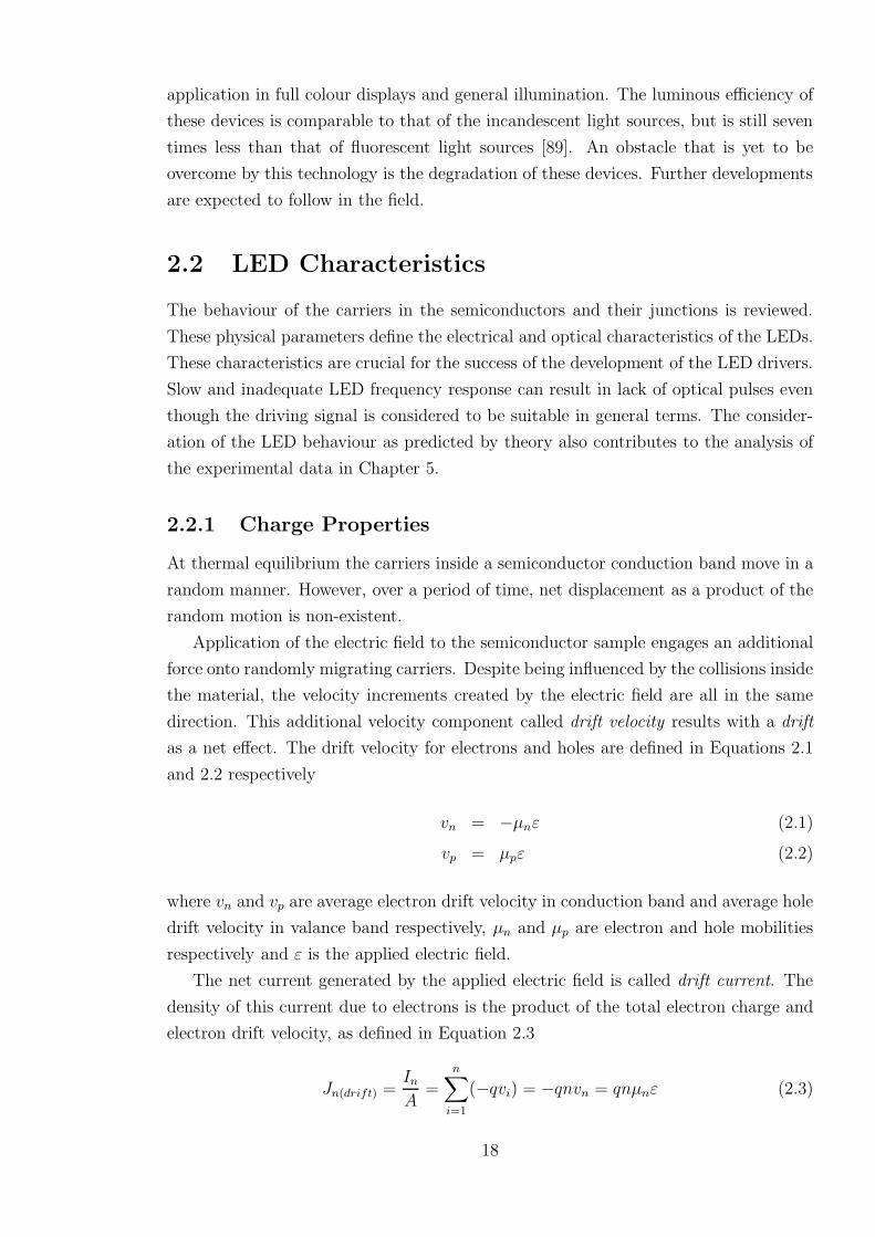
the positive towards the negative charge (Figure 2.2).
With no external excitation being present, the drift current due to the electric
field and the diffusion current due to the concentration gradient must exactly cancel
each other. Comparison of the drift and diffusion currents results in the need for a
constant Fermi level through the sample in order to satisfy zero net current (Figure
2.2). The Fermi level determines the energy at which the probability of occupation
by an electron is one half. The need for constant Fermi level results in unique space
charge distribution in the junction [90].
When the p−n junction is reverse biased, a very small current flows through. The
reason is that only the minority carriers on each side have right polarities to carry cur-
rent across the junction. Consequently, the minority carrier distribution is disturbed
as the minority carriers are depleted from the junction. Similarly, the carrier injec-
tion, through either optical excitation or electrical bias, results with the change in the
minority carrier density distribution. Because of the diffusion of minority carriers the
changes in the minority carrier concentrations caused by a bias voltage are not localised
at the edges of the depletion layer [91]. Instead, the minority carrier concentration has
the spatially dependent variations as shown in the Figure 2.3 (rearranged from [90]
and [91]), where the first letter in the carrier concentration denotes carrier type and
the subscript denotes material type.
20
Figure 2.2: Energy band diagrams for doped semiconductors and a p-n junction
Figure 2.3: Majority and Minority Carrier Distribution
The spatially dependent variations of the minority carrier concentration across the
diffusion regions are described by Equations 2.15 and 2.16.
np(x) − np0 = np0
[
exp
(
qV
kT
)
− 1
]
exp
(
x + xp
Ln
)
(2.15)
pn(x) − pn0 = pn0
[
exp
(
qV
kT
)
− 1
]
exp
[
−
(
x − xn
Lp
)]
(2.16)
In the Equations 2.15 and 2.16 q is the elementary charge, k is Boltzmann’s constant,
T is temperature, Ln and Lp are minority carrier diffusion lengths defined in Equations
2.17 and 2.18.
Ln =√
Dnτn (2.17)
Lp =√
Dpτp (2.18)
In the Equations 2.17 and 2.18 τn and τp are the excess minority carriers’ lifetimes. For
21

low carrier injection, those two lifetimes are comparable quantities [92]. The minority
carrier lifetime is the inverse constant of proportionality that relates recombination
rate to the carrier concentration. Thus, a short lifetime corresponds to a high recom-
bination rate. During recombination the number of minority carriers in the sample
decay exponentially. The minority carrier lifetime is the time constant that defines the
decay [90].
Whenever the non−equilibrium is established the carriers attempt to achieve their
respective equilibrium concentration. Contrary to the carrier generation process occur-
ring during the reverse biasing, the mechanism that restores equilibrium following the
injection of the excess carriers is the recombination of the excess minority carriers with
the majority carriers. The nature of the recombination process determines the form in
which the energy is released. This could be either in the form of radiating photons or
phonon dissipation to the lattice. In order for a material to be utilisable for efficient
photon generation its band structure needs to be direct [90]. Such semiconductors
have no momentum difference between the minimum of their conduction band and
the maximum of their valence band, as shown in Figure 2.4. This arrangement allows
direct transition of an electron either upward or downward with no need to change its
momentum. In contrast when an electron makes an indirect transition it has to absorb
or emit a phonon, thereby exchanging energy and momentum with the crystal lattice,
in order to complete the transition [91]. Recombination phenomena can be classified
as direct and indirect process - each dominating in direct and indirect semiconductors
respectively. LEDs and lasers require direct semiconductors for efficient photon gener-
ation [90]. Regardless of the recombination type, the net result of any recombination
process is release of energy by an electron when dropping from a higher to a lower
energy level.
Figure 2.4: Simplified Energy-momentum diagram
22

2.2.3 Electrical Properties
Diode current and capacitance are considered as the most crucial electrical character-
istics for the proposed application. The relationship between the current and voltage
defines the amplitude of the driving signal required for successful light generation. The
capacitance significantly affects the speed of the diode response. The theoretical con-
sideration of the practical diode is included because of the experimental nature of the
project.
Junction Current
The total potential generated by the space charge region (Figure 2.2) is called built in
potential, vbi and is defined in Equation 2.19.
vbi =kT
qln
(
NAND
n2i
)
(2.19)
As the majority carrier concentration equals the doping concentration at thermal equi-
librium (i.e. nn0 = ND and pp0 = NA), using the mass action law (pp0nn0 = n2i ) [90]
Equation 2.19 is rearranged into Equation 2.20.
vbi =kT
qln
(
pp0nn0
n2i
)
=kT
qln
(
nn0
np0
)
(2.20)
Assuming that the carrier densities at the boundaries are related to the electrostatic
potential difference across the junction [90], Equation 2.20 can be rearranged into
Equation 2.21 where V is the applied voltage. The sign of the applied voltage is
positive for the forward bias and negative for the reverse bias.
nn = np exp
[
q (vbi − V )
kT
]
(2.21)
Minority carrier densities at the boundaries of depletion layer can be obtained (2.22
and 2.23) from the Equation 2.20 considering the low-injection condition for which the
number of injected minority carriers is much smaller than the majority carrier density
(nn ≈ nn0 and pp ≈ pp0) [90].
np − np0 = np0
[
exp
(
qV
kT
)
− 1
]
(2.22)
pn − pn0 = pn0
[
exp
(
qV
kT
)
− 1
]
(2.23)
Using the Equations 2.22 and 2.23 the hole and electron currents at the boundaries
can be defined by Equations 2.24 and 2.25 where the diffusion coefficients, Dn/p, are
23
defined by Equation 2.6 and the diffusion lengths, Ln/p, are defined by Equations 2.17
and 2.18. It follows that the diffusion currents fall exponentially with the diffusion
lengths. The total current in the device must be constant and it is equal to the sum
of the two current components (Equation 2.26).
Jp(xn) =qDppn0
Lp
[
exp
(
qV
kT
)
− 1
]
(2.24)
Jn(−xp) =qDnnp0
Ln
[
exp
(
qV
kT
)
− 1
]
(2.25)
J = Jp(xn) + Jn(−xp) (2.26)
Incorporating Equations 2.24 and 2.25 into Equation 2.26 results with the total ideal
diode current density relationship shown in Equation 2.27. Js is the saturation current
density with its value being defined in Equation 2.28.
J = Js
[
exp
(
qV
kT
)
− 1
]
(2.27)
Js =qDppn0
Lp+
qDnnp0
Ln(2.28)
As I = JA, Is = JsA and the specified area is fixed then the ideal diode current is
defined by Equation 2.29.
I = Is
[
exp
(
qV
kT
)
− 1
]
(2.29)
This section highlights the standard semiconductor theory relevant to the applica-
tion. The deviations from the ideal theoretical characteristics are considered in the
following section.
Deviation from Ideal Characteristics
The ideal diode equation (Equation 2.29) describes current voltage characteristic for
p-n junction diodes at low current densities [90]. A more realistic solution to diode
current-voltage characteristic includes an ideality factor η, the voltage drop across its
internal resistance Rs and current flow through diode parallel resistance Rp. The result
is a more realistic diode equation (Equation 2.30). This equation can be rearranged
into Equation A.26, so that diode current is the subject of the equation (as shown in
appendix A).
I = Is
exp
[(
q(V − IRs(V ))
ηkT
)]
− 1
+V − IRs(V )
Rp(V )(2.30)
The ideality factor takes into account the generation and recombination processes in
the depletion layer of a diode. These are ignored in the ideal diode equation due to
24

an assumption that neither of those two processes occurs in this region. Theory shows
the value for the ideality factor lies between 1 and 2 [91, 93]. A detailed analysis shows
that the ideality factor tends to being equal to 2 at high injection levels [91]. However,
in practice the ideality factor can be higher than this theoretically predicted value [94].
It can be as high as 7 when considering GaN based diodes [95].
Ideally the series resistance should be zero. However, in practice it appears as a
product of the resistance of the neutral regions and internal contact resistance [96]. The
value of the series resistance for a particular diode can be established from Equation
2.31. The derivative needs to be taken at the voltages significantly larger than the
diode threshold voltage where the slope of the I-V curve is relatively constant.
Rs,p(V ) =dV
dI(2.31)
The parallel resistance is an outcome of any conduction channel that bypasses the p-n
junction. This is normally a consequence of damaged regions and surface imperfections
[96]. To find the value of the parallel resistance the relationship shown in Equation
2.31 is also valid. In this case the derivation is performed in the reverse bias section of
the I-V characteristic. Ideally the parallel resistance should be infinitely high. Apart
from controlling the slope of the diode I-V characteristic in the reverse bias region, this
resistance also affects the slope of the same curve at low forward bias voltages where
the value of the parallel resistance is comparable to the diode dynamic resistance. The
second term in the expression for the practical diode (Equation 2.30) represents the
current flowing through the parallel resistance. It normally has negligible contribution
in forward bias.
The I-V characteristic generated from the practical LED equation (2.30) is shown
in Figure 2.5. Even though the plot might appear to be purely exponential it is in fact
broken into distinctive exponential regions (as shown in Figure 2.6). The diode current
follows the parallel resistance current at reverse bias and low forward bias. It then
behaves according to the rules described by the standard diode equation. At larger
forward bias, the diode current asymptotically approaches the behaviour of the diode
series resistance current. The regions and the way the plots are derived are described
in appendix A in detail.
Capacitance - Voltage Relationship
The LED capacitance behaviour is important in the fast pulsing applications because
this characteristic has a potential of preventing the generation of light. It was exper-
imentally determined that some of the devices that fail to produce fast light pulses
also have increased capacitance. There are two types of capacitance associated with a
p-n junction: junction or depletion layer capacitance and charge storage or diffusion
25

−1 −0.5 0 0.5 1 1.5 2 2.5 3 3.5
0
0.01
0.02
0.03
0.04
0.05
0.06
0.07
Voltage [V]C
urre
nt [A
]
Figure 2.5: Practical LED I-V relationship
−1 −0.5 0 0.5 1 1.5 2 2.5 3
−22
−20
−18
−16
−14
−12
−10
−8
−6
−4
−2
Voltage [V]
ln(I
)
ln(Ipractice
)
ln(Irseries
)
ln(Irparallel
)
ln(Itheory
)
Figure 2.6: Practical LED ln(I)-V relationship (scale arbitrary)
capacitance.
The depletion layer holds negative space charges on the p side and positive space
charges on the n side [91]. The dipole that is the result of this charge storage distri-
bution causes the junction depletion layer capacitance [97]. The depletion capacitance
per unit area is defined as the rate of change of depletion layer charge per unit area,
dQ, with respect to change of the applied voltage, dV , (Equation 2.32).
Cj =dQ
dV(per unit area) (2.32)
Increasing the reverse bias voltage across the p-n junction results in increment of the
depletion layer width, W (see Figure 2.3). The incremental space charges on the n
and p sides of the depletion layer are equal, but with opposite charge polarity, thus
maintaining overall charge neutrality. This incremental charge causes an increase in
the electric field by an amount defined by Equation 2.33 where ǫS is semiconductor
26

dielectric permittivity [90].
dε =dQ
ǫS(2.33)
Thus Equation 2.32 can be developed into Equation 2.34.
Cj =dQ
dV=
dQ
W dQǫS
=ǫS
W=> Cj =
ǫS
W(2.34)
The expression for the depletion capacitance per unit area (Equation 2.34) is identical
to the standard expression for a parallel plate capacitor. The spacing between the two
plates represents the depletion layer width. The equation is valid for any arbitrary
impurity distribution.
For one sided abrupt junction, the junction width is defined as shown in Equation
2.35.
W =
√
2ǫS(vbi − V )
qNB(2.35)
Combining Equation 2.35 into Equation 2.34, the junction capacitance expressed in
terms of applied voltage and material properties can be found (Equation 2.36) and it
can be rearranged into Equation 2.37.
Cj =
√
qǫSNB
2(vbi − V )(2.36)
1
C2j
=2(vbi − V )
qǫSNB(2.37)
The Equation 2.36 allows the use of plot of C−2j versus V for experimental determina-
tion of the material properties from a ready made device. The plot produces a straight
line for a one sided abrupt junction. The slope gives the impurity concentration NB
of the substrate and the intercept (at C−2j = 0) gives built in voltage, vbi [90]. Similar
equations can be developed for the linearly graded and the parabolic junctions.
To derive Equation 2.37 it is assumed that the only variation of the space charge in
the depletion layer contributes to capacitance. This certainly is a good assumption for
the reverse bias condition. For forward bias, however, the applied voltage effectively
reduces the built in potential and hence the built in field which prevents excessive
diffusion. A large current, in the form of excess minority carrier, can flow across the
junction corresponding to a large number of mobile carriers present within the neutral
region. Once injected, the minority carriers recombine with the majority carriers and
decay exponentially with the distance. These minority carrier distributions lead to
current flow and to charge storage in the p-n junction [90]. The storage of these
mobile carriers in diffusion region with respect to the biasing voltage contributes to an
additional term, called the diffusion capacitance.
27

The number of stored minority carriers depends on the diffusion length and the
charge density at the boundary of the depletion region. The charge of the stored
minority carriers can be found by integrating the excess carriers in the neutral regions.
These are represented by the shaded areas in Figure 2.3. The stored charges per unit
area are defined in the Equations 2.38 and 2.39.
Qn = qLnnp0
[
exp
(
qV
kT
)
− 1
]
(2.38)
Qp = qLppn0
[
exp
(
qV
kT
)
− 1
]
(2.39)
The stored charge can also be expressed in terms of the injected current. The amount
of the stored charge is the product of the current and the minority carrier lifetime
(Equations 2.40 and 2.41).
Qn =L2
n
Dn
Jn(xp) = τnJn(xp) (2.40)
Qp =L2
p
Dp
Jp(xn) = τpJp(xn) (2.41)
The same relationship from Equation 2.32 is used to define the diffusion capacitance.
However if the junction area is to be considered (Equation 2.42), then the diffusion
capacitance is expressed as show in Equation 2.43.
Cd = AdQp
dV(2.42)
Cd =Aq2Lppn0
kTexp
(
qV
kT
)
(2.43)
Under reverse bias, the diffusion capacitance becomes inconsequential because of the
negligible minority carrier storage.
2.2.4 Optical Properties
Had the electroluminescence effect in the LEDs been an instantaneous process with
100% efficiency, it could have been said that the LEDs operation depends on their
electrical characteristics only. However, the practical limitations are defined by the
optical characteristics. The most important ones in the case of the LEDs are light
emission, absorption and interaction between light and changes in refractive index [98].
The most important optical features required for PMT calibration are the light
intensity and the speed at which the optical pulses are switched. The relationship be-
tween the LED light intensity and its injection current is roughly linear. Nonlinearities
in the relationship are usually found at very low and very high current levels [91]. This
28
is caused by the variation in LED radiative efficiency. This factor starts from being low
at low injection currents and it increases with the current increase. It finally saturates
at higher injection rates. Due to the low non-linearity and desired simplification, it is
generally accepted that the intensity – current relationship is linear. This assumption
allows a simple estimate of the LED output intensity if the current flowing through the
device is known.
Theoretically, the radiation efficiency at any temperature is proportional to the
number of electrons and holes present in the material as shown in Equation 2.44,
where β is the constant of proportionality [92].
R = βnp (2.44)
In principle, LEDs are nearly 100% efficient internally. By the time the light leaves the
outer surface of the device, this efficiency is significantly reduced because of the material
properties. Similarly, the material properties limit the speed at which the devices react
to the driving signal. The time response of the optical signal is subject to the physical
characteristics of the device itself. It is not possible to realise instantaneous switching
between the on and off states. The optical output is a result of the recombination
process. The time the carriers take to travel across the depletion region together with
the time carriers take to recombine, represents a delay between the stimulating current
pulse and generation of the optical signal. A comparatively small additional delay is
caused by the optical signal propagation to the outer surface of the device. When
the electrical signal to the junction is removed the excess minority carriers contained
within the junction take a finite time to recombine with the majority carriers. Thus
they are responsible for the exponential turn off decay [90].
Generally, it is expected that the rise of the optical signal should closely follow in
shape its electrical counterpart, but after a certain time delay. The removal of the
electrical pulse does not necessarily imply an immediate disappearance of the optical
signal. More detailed consideration of the LED transient responses is studied in Section
3.3.
2.3 Advanced Structures - High Brightness LEDs
In a pursuit of improved electrical and optical characteristics of the LEDs, different
types of junctions have been developed. These are split into groups: homojunctions,
heterojunctions and metal - semiconductor junctions. Different doping in the same
semiconductor forms a homojunction, while a heterojunction is created using at least
two different materials. A metal-semiconductor junction is produced using a metal and
semiconductor.
29

Heterojunctions are a direct product of the need for improvement in light intensity.
A heterojunction is normally formed between two lattice-matched semiconductors of
dissimilar energy bandgaps. The junctions are named using lowercase for conductiv-
ity type of the smaller bandgap material in combination with the uppercase for the
conductivity type of the larger bandgap material. Depending on which conductivity
types of the materials are employed, these junctions can be either isotype (p-P, n-N)
or anisotype (p-N, P-n). The two most common types of heterostructures are Single
Heterojunction (SH) and Double Heterojunction (DH).
The same mathematical relations regarding the depletion layer, the carrier distri-
bution, the current-voltage characteristics and capacitance are valid for both homo-
junctions and heterojunctions [91]. The additional resistance can be caused by contact
resistance, resistance caused by the abrupt heterostructures and bulk resistance oc-
curring particularly in the materials with low carrier concentrations or low carrier
mobilities [96]. A voltage drop occurs at the series resistance thereby increasing the
drive voltage [96].
2.3.1 Single Heterojunction
Single heterojunctions are used with the aim of controlling distribution of excess mi-
nority carriers through restriction of the diffusion length. Normally a P-p-n diode is
formed with heavily doped n region. Consequently, electron injection completely dom-
inates hole injection. The P-p heterojunction restricts electron diffusion and confines
them to the narrow gap p region (Figure 2.7). This becomes the active region. Its
thickness is controlled by the location of the P-p heterojunction with respect to that
of the p-n junction [91].
Figure 2.7: SH and DH energy bands and excess carrier distribution
30

2.3.2 Double Heterojunction
Improved electrical and optical confinement is possible when a DH is employed. These
devices are either P-p-N or P-n-N. Most of the injected excess carriers are collected
in the narrow gap where they are bounded by the energy barriers on both sides, as
shown in Figure 2.7. Typically, this active layer is under 100nm wide. Compared to
the active layer of a homostructure that has a thickness of the order of 1µm or larger,
which is determined by the electron diffusion, this tight carrier confinement creates a
much higher carrier concentration for a given injection current [91]. The achieved high
carrier concentration results in high radiative efficiency of the recombination process.
As the radiative recombination rate is given by the bimolecular recombination equa-
tion (Equation 2.44) it is clear that a high carrier concentration in the active region
increases the radiative recombination rate and decreases the recombination lifetime
[96]. Consequently, all high intensity LEDs employ heterojunctions.
The optical energy of the generated photons is lower than the energy bandgap of the
barriers (Figure 2.8). Consequently, the barriers are transparent to the light emitted
by the active layer. This reduction of absorption loss makes DH devices also optically
superior over their SH and homojunction counterparts.
2.3.3 Single Quantum Well - InGaN Based LEDs
A quantum well (QW) device is a variation of DH. It is formed when the layer between
two barriers is thin enough to cause quantisation of energy. This results in discrete
energy levels associated with the motion of electrons and holes, as shown in Figure 2.8
[91].
The simplest possible structure employing this effect is a single quantum well
(SQW). It consists of a thin layer of narrow gap semiconductive material sandwiched
between thicker layers of a wider gap material. This layer formation causes an in-
crease of carrier concentration in the quantum well region thus increasing the number
of carrier interactions. The injected carriers are more concentrated in a quantised sub-
band of a quantum well than in the entire band of a bulk semiconductor [91]. The
emitted light intensity increase makes the SQW one of the basic building blocks for
optoelectronic devices. This is the most common structure used for manufacture of
high brightness LEDs. The simplified energy band diagram of the device is shown in
Figure 2.8.
The operation of the quantum well largely depends on the length of the quantum
well (lQW ) as it is required to be sufficiently small in order to create size quantisation.
If the active layer is thin enough, the motion of carriers in the direction perpendicular
to the heterointerfaces is quantised. That is, this motion involves discrete (quantum)
energy levels [99, pp99-103].
31

Figure 2.8: Single Quantum Well Energy Band Diagram
The energy of the transmitted photons and wavelength of the transmitted light
also depend on the length of the quantum well. The quantised electrons and holes
contribute to energy band gap of the newly formed material as the new energy band
gap is equal to the sum of well material band gap and electron/hole quantised energies,
as shown in Equation 2.45. The selection rules for optical transitions of electrons
between quantised conduction sub-bands and quantised valence sub-bands require that
only transitions between a conduction sub-band and a valence sub-band of the same
quantum number are allowed [91]. It can be seen, from Equation 2.45 and from Figure
2.8, that the emission energy caused by the quantum well is not the same as the
emission energy of either of the two materials employed. This limited independence of
the emitted light energy and hence wavelength, makes the SQW devices an attractive
solution for manufacture of light emitting devices operating at wide range of emission
wavelengths, but using the same technology. This allows freedom to design required
emission wavelengths.
EgQW = Eg(well) + Ec1 + Ev1 = hν (2.45)
Following the laws of quantum physics, it can be shown [92] that the precise expression
for the energy band gap of the quantum well is defined by Equation 2.46, where m∗
r is
reduced effective mass expressed in Equation 2.47 in terms of electron m∗
e and hole m∗
h
effective masses.
EgQW = Eg(well) +h2
8m∗
rl2QW
(2.46)
m∗
r =m∗
em∗
h
m∗
e + m∗
h
(2.47)
The structure of SQW devices also restricts the possibility of surface recombination
because the carriers are enclosed inside of the well and are less likely to escape through
32
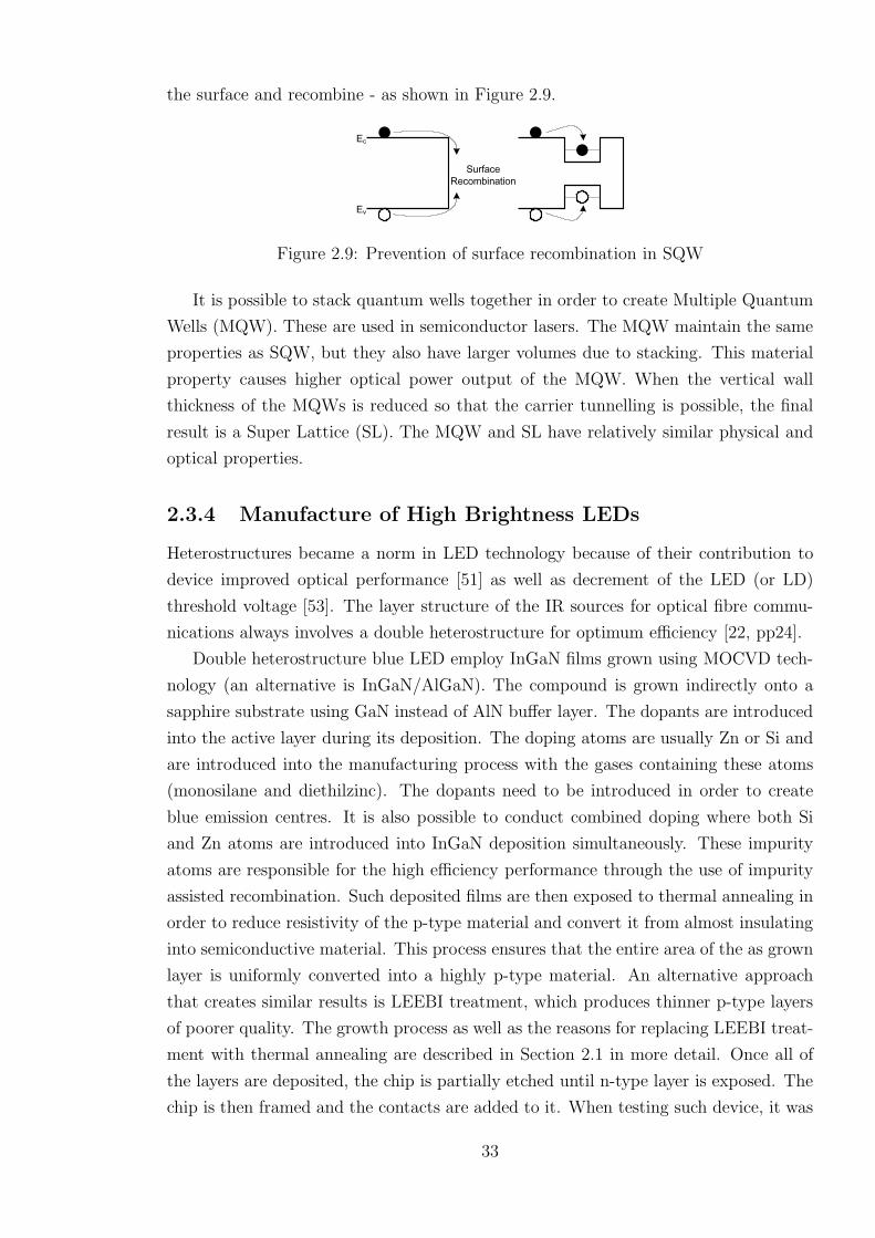
the surface and recombine - as shown in Figure 2.9.
Figure 2.9: Prevention of surface recombination in SQW
It is possible to stack quantum wells together in order to create Multiple Quantum
Wells (MQW). These are used in semiconductor lasers. The MQW maintain the same
properties as SQW, but they also have larger volumes due to stacking. This material
property causes higher optical power output of the MQW. When the vertical wall
thickness of the MQWs is reduced so that the carrier tunnelling is possible, the final
result is a Super Lattice (SL). The MQW and SL have relatively similar physical and
optical properties.
2.3.4 Manufacture of High Brightness LEDs
Heterostructures became a norm in LED technology because of their contribution to
device improved optical performance [51] as well as decrement of the LED (or LD)
threshold voltage [53]. The layer structure of the IR sources for optical fibre commu-
nications always involves a double heterostructure for optimum efficiency [22, pp24].
Double heterostructure blue LED employ InGaN films grown using MOCVD tech-
nology (an alternative is InGaN/AlGaN). The compound is grown indirectly onto a
sapphire substrate using GaN instead of AlN buffer layer. The dopants are introduced
into the active layer during its deposition. The doping atoms are usually Zn or Si and
are introduced into the manufacturing process with the gases containing these atoms
(monosilane and diethilzinc). The dopants need to be introduced in order to create
blue emission centres. It is also possible to conduct combined doping where both Si
and Zn atoms are introduced into InGaN deposition simultaneously. These impurity
atoms are responsible for the high efficiency performance through the use of impurity
assisted recombination. Such deposited films are then exposed to thermal annealing in
order to reduce resistivity of the p-type material and convert it from almost insulating
into semiconductive material. This process ensures that the entire area of the as grown
layer is uniformly converted into a highly p-type material. An alternative approach
that creates similar results is LEEBI treatment, which produces thinner p-type layers
of poorer quality. The growth process as well as the reasons for replacing LEEBI treat-
ment with thermal annealing are described in Section 2.1 in more detail. Once all of
the layers are deposited, the chip is partially etched until n-type layer is exposed. The
chip is then framed and the contacts are added to it. When testing such device, it was
33
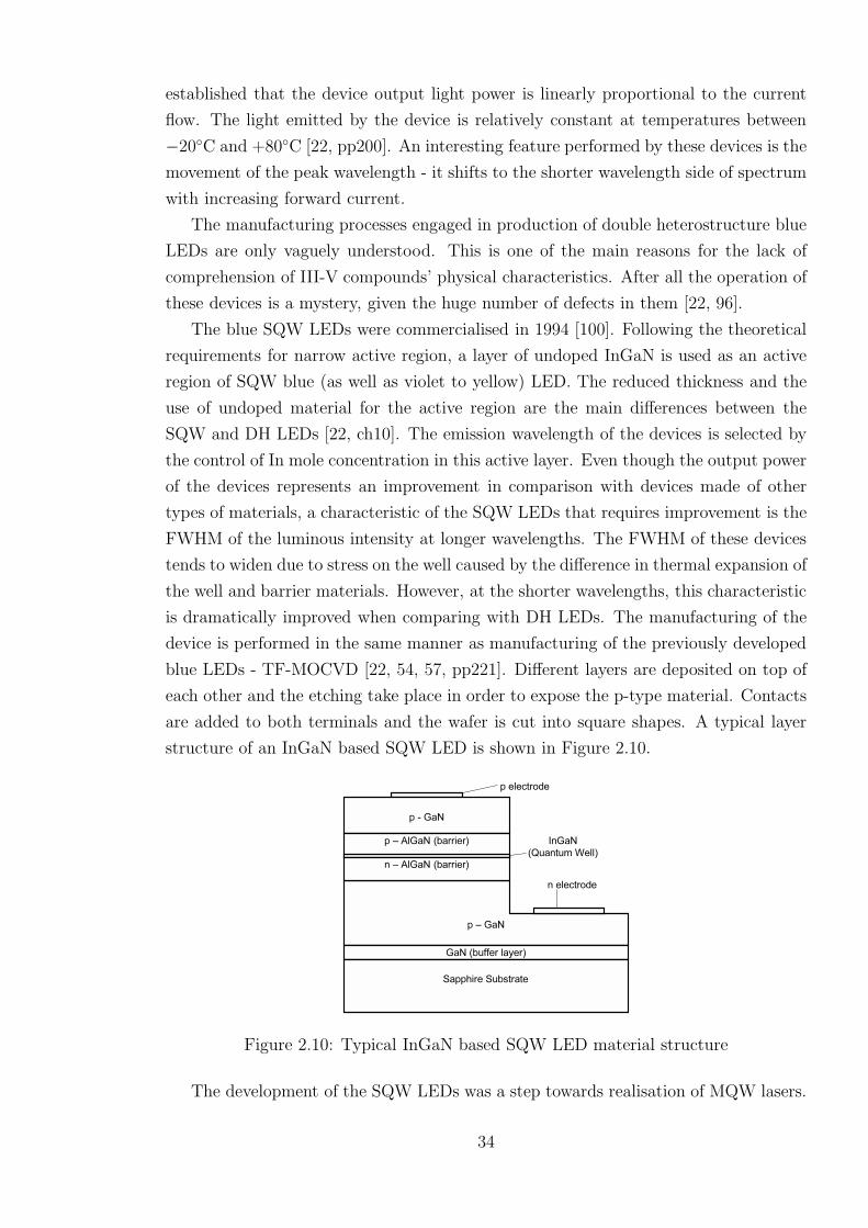
established that the device output light power is linearly proportional to the current
flow. The light emitted by the device is relatively constant at temperatures between
−20C and +80C [22, pp200]. An interesting feature performed by these devices is the
movement of the peak wavelength - it shifts to the shorter wavelength side of spectrum
with increasing forward current.
The manufacturing processes engaged in production of double heterostructure blue
LEDs are only vaguely understood. This is one of the main reasons for the lack of
comprehension of III-V compounds’ physical characteristics. After all the operation of
these devices is a mystery, given the huge number of defects in them [22, 96].
The blue SQW LEDs were commercialised in 1994 [100]. Following the theoretical
requirements for narrow active region, a layer of undoped InGaN is used as an active
region of SQW blue (as well as violet to yellow) LED. The reduced thickness and the
use of undoped material for the active region are the main differences between the
SQW and DH LEDs [22, ch10]. The emission wavelength of the devices is selected by
the control of In mole concentration in this active layer. Even though the output power
of the devices represents an improvement in comparison with devices made of other
types of materials, a characteristic of the SQW LEDs that requires improvement is the
FWHM of the luminous intensity at longer wavelengths. The FWHM of these devices
tends to widen due to stress on the well caused by the difference in thermal expansion of
the well and barrier materials. However, at the shorter wavelengths, this characteristic
is dramatically improved when comparing with DH LEDs. The manufacturing of the
device is performed in the same manner as manufacturing of the previously developed
blue LEDs - TF-MOCVD [22, 54, 57, pp221]. Different layers are deposited on top of
each other and the etching take place in order to expose the p-type material. Contacts
are added to both terminals and the wafer is cut into square shapes. A typical layer
structure of an InGaN based SQW LED is shown in Figure 2.10.
Figure 2.10: Typical InGaN based SQW LED material structure
The development of the SQW LEDs was a step towards realisation of MQW lasers.
34
Even though the aim was an LD, the LEDs have benefited from this tendency to
improve the materials and techniques used for LD development.
2.4 Applications
LEDs are considered the ultimate general source of continuous light due to their high
luminescence efficiency, quick response time and long lifetime [22]. Most commonly,
the LEDs are used as indicators and displays. However they do have wide application
range - some of its uses are shown in table 2.1.
Application ExampleTelecommunications fibre optics light sourceElectronics erasing EPROM (UV)Semiconductors manufacturing definition of mask patterns for wafersEnvironmental UV air purifier, UV decomposition
of toxic substancesTransport traffic lights, street lighting, vehicle
lightsSecurity chemical detection, emergency lights,
forgery detectionMedicine test equipment, cancer treatment,
human genome analysisHome appliances indicators and displays, TV sets, phonesAdvertising displaysMeasurements indicatorsOffice Equipment printers, scanners
Table 2.1: Common LED applications
LED application can mainly be split into three general groups: displays, indicators
and in more recent years lighting.
In the past, prior to the development of the LEDs, small incandescent lamps were
used as the front panel indicators. First application of LEDs involved their use in
scrolling red light messages on a black background. These were obviously used for
displaying purposes. With the time, these simple apparatus evolved into three-colour
displays as amber and green LEDs were finding their way into the market. LED use
for digital displays (most commonly as 7-segment displays, but also in the form of 16-
segment displays for alphanumeric outputs or as dot-matrix displays) allowed messages
to became more complex too, as they developed into animations as well as the simple
scrolling letters. A disadvantage that was hanging over the use of LEDs was that they
were definitely indoor devices. With time, this changed as brighter and more robust
devices were developed, so that these products could be used for outdoor purposes as
well because of the increased brightness in relation to ambient sunlight.
35
One of the greatest disadvantages that followed LEDs for a long time through their
development was the inability to produce true-colour. The reason for lack of such
ability came from the fact that no blue light could be produced with the use of LEDs.
This changed in the 1990s with the advancement in green and blue light emitting
technology. The capability to produce green and blue colours permitted creation of
full colour displays with the use of the three primary colours (red, green and blue).
By mid-1990s, LED technology was sufficiently developed to support practical ap-
plication of full-colour animation displays. Alongside the invention of new devices that
were outperforming their predecessor in the wavelength aspect of the LED character-
istic, the LED brightness levels were significantly improved as well. This meant that
mono-colour traffic signals and other similar applications that require the brightest
LEDs possible are nowadays achievable. The high brightness blended with weather-
resistant packaging makes the LEDs supreme devices for such applications as traffic
signals, speed limit signs, stadium scoreboards or advertising for example.
The size and the lifetime are also the factors that contributed to the inclusion
of LEDs in telecommunication systems. They do have disadvantages when used as
such: poor intensity, lacking ray focus, low-modulation bandwidth, and incoherent
radiation when contrasted against laser diodes. These disadvantages have forced LEDs
to be applied into relatively low-bandwidth short-distance networks such as Local Area
Networks (LANs). The communication means for such networks are fibre optics cables.
On the other hand space propagation based optical transmission systems, that do
not require any cables or electrical waves, can be set up at relatively short range. The
interference imposed by sunlight and light producing devices makes the range be a
very important limiting factor in such systems. Hence, such sort of communication
is advisable under special conditions - i.e. darkened environment. Alternatively, UV
LEDs can be employed in order to slightly extend this range, as the influence of sunlight
and fluorescent lamps becomes rapidly weakened at wavelengths shorter than 380nm.
As previously stated some of the major advantages of LEDs are their energy effi-
ciency and lifetime. When compared with conventional light bulbs, their power con-
sumption is reduced by at least factor of ten. Concurrently, LEDs are likely to operate
in normal conditions for up to ten times longer than the standard light bulbs do. These
are the reasons for many to believe that LEDs are to become light sources for the future.
The other advantages that LEDs have over conventional light bulbs include be-
ing environmentally friendly (lifetime, material, size) and having a superior response
speed. This technology is already introduced into a broad range of applications such
as illumination, backlights and decorative lighting.
36
2.5 Chapter 2 Summary
The technological evolution of the LEDs prescribed the grounds for the physical char-
acteristics of the devices. The structure of the current devices is largely determined
by the historic search for the materials and manufacturing methods that would satisfy
market trends at the time. The resulting limited functionality does not necessarily
allow the use of these devices in fast pulsing applications. The appropriateness of the
devices for the proposed application is investigated in the following chapters. The
construction of LEDs is important for the background understanding of the electrical
and optical properties of the devices in question. This chapter touched upon the man-
ifestation of these electrical and optical characteristics. These informed about possible
LED theoretical responses to the driving signals. The device current, capacitance and
optical generation are of the main interest for the application. All these properties are
defined by the behaviour of the charge carriers in the LEDs.
The structure of the advanced devices informed about possible complications caused
by the still progressing and not fully understood technology. The LED applications
showed the direction the LEDs have followed. Chapter 3 considers the response of
these devices to pulses and the methods employed for creation of adequate LED driving
signals.
37

Chapter 3
Pulse Shaping Techniques and LED
Pulse Response
This chapter focuses on the methods of pulse generation and subsequent shaping. Ex-
isting techniques are studied. Some of the techniques used by the standard LED drivers
are experimentally determined with no full theoretical appreciation of their operating
principles publicised. The techniques are theoretically analysed in order to determine
their suitability for the intended LED driver. The techniques are altered and optimised
for the intended application. The optimisation is based on the developed theoretical
understanding of the operating principles. The developed methodology is employed as
described in Chapter 6. The aim of this research is to generate switching techniques
that would overcome some of the problems caused by physical responses of LED to
fast electronic “turn on” pulses. The main focus of this work is the creation of an
optical signal that would satisfy the requirements for high speed PMT calibration and
the simulation of optical signals encountered by Cherenkov radiation detectors. The
work differs from the standard reported techniques in that it is completely focused on
the theoretical understanding of the techniques and their applicability to the LEDs as
opposed to the ad hoc methods.
Generally, the shape of the optical pulses generated by LEDs is governed by the
driving signal parameters. However, at higher switching speeds the output optical
pulses are dictated by the LED physical properties. This switching process takes finite
amount of time, which is determined by the device quantum characteristics. The fast
pulse response of the LED is considered in detail in Section 3.3.
3.1 Types of LED Drivers
The review of the pulse generating circuits [101–119] shows that in order to obtain
fast optical pulses the LED drivers very commonly rely on the simple concept of dis-
38
charging capacitor through a fast switch (as described in Section 3.4). A few groups of
circuits are identified as possible foundation for the LED drivers. These are described
in the following sections. A number of potential LED drivers are considered in this
chapter. These are: multivibrators, emitter-coupled monostable, avalanche transistor
based drivers and a complementary transistor pair regenerative switch.
3.1.1 Multivibrators
Multivibrators [103–107, 120] are circuits commonly used for creation of (rectangu-
lar) pulses. They rely on the use of regenerative transistor switches. They are split
into three groups: bistable, monostable and astable. There is also a special case of
multivibrators, which are used as Schmitt Triggers.
It is the regenerative action of the monostable and possibly astable multivibrators
that could play an important role in creation of fast optical pulses. The quasi-stable
states of those vibrators are determined by the passive components in the circuit.
These states inevitably stop with no aid from an external signal. Hence if triggered (in
monostable case) and if the time from the beginning to the end of the quasi-state can
be reduced to the required period then the circuit could be used as a basis for an LED
driver. One of the primary uses of monostable multivibrators is creation of pulses well
defined in amplitude and duration when incoming pulse is weak or ill defined [103].
The simplicity of multivibrator circuits is seen as an advantage that could poten-
tially be exploited for generation of the required optical pulses. However, the exper-
imental work has resulted in relatively poor pulse timing when compared with the
other techniques that are considered in this chapter. It is concluded that the discharg-
ing time constants in the circuits are much higher than what would be tolerable to
generate adequate optical pulses.
3.1.2 Emitter Coupled Monostable
The emitter coupled monostable [103, 108–110, 120] is a variation of multivibrators
derived because of its speed, improved linearity and stability. The width of the output
pulses is linearly dependant on the trigger voltage. Simultaneously, this width is also
controlled by the passive components in the same manner as for the other multivibra-
tors. This pulse width dependence on the passive components provides an advantage
for the multivibrators, as their output can easily be repeatable due to the passive
component value accuracy.
An advantage that the emitter-coupled monostable could provide over the other
pulse drivers lies in the fact that its output can easily be pulled below the ground
level. This would provide the load LED a chance for its current to be swept out of the
depletion layer (see Section 3.3).
39

The emitter coupled configuration was in the past a basis for conventional digital
circuits. The Emitter-Coupled Logic (ECL) circuits were at one point the fastest
conventionally available digital circuits [110].
The experimental work performed on the emitter coupled monostable circuits has
generated improved pulse timing in relation to that of the standard multivibrators.
This is mainly attributable to the ability of those circuits to pull the signal below
ground level before the switched signal approaches its slowest section. This estab-
lishes reverse bias across the LED so that the optical pulse is cut off early. However,
the experimentally achieved pulses are deemed to be slower than required, hence the
technique was abandoned.
3.1.3 Avalanche Transistors
When the reverse bias across a p-n junction is increased to the junction breakdown
level, the diode conducts very large current. Even though this process is not necessarily
destructive, the maximum current must be limited in order to avoid excessive junction
heating. This is why the avalanche breakdown represents the upper limit of the p-n
junction reverse bias [90].
Reverse bias provides increase of the depletion layer electric field. This electric
field causes sweep of the minority carriers across the junction (and hence saturation
current). If an electron (p-type minority carrier) is attracted by the electric field, it
accelerates across the depletion layer. It is likely that this electron collides with a
crystal (or impurity) atom in the depletion region delivering its kinetic energy to the
atom with which it collides. However, if the electric field is increased so much so that
the electron gains enough energy to break covalent bonds, than it causes creation of the
electron-hole pair [121]. The newly formed pair gains more energy from the electric field
causing creation of more electron-hole pairs. The process continues in the avalanche
manner for as long as the avalanche conditions are maintained.
It is reported that the LED avalanche breakdown as well as the use of avalanche
transistors for LED driving makes it possible to obtain sub-nanosecond light pulses
[13, 109, 116–119]. However, it was found that the number of emitted photons in such
case is limited to several hundreds, thus limiting the possibility for application of the
driver. A few avalanche transistors can be used in series in order to gain enough current
to drive the load LED with required pulse height [116].
The failure of the avalanche transistor circuits to provide repeatable and reliable
pulses is the main reason for rejection of this technique as a possible candidate for
development of the LED driver in this case.
40

3.1.4 Complementary Transistor Pair Regenerative
Switch
A successful light pulse generator based on PNP-NPN regenerative switch (Section
3.4) is reported by Kapustinsky et al. [14]. It provides sufficient current to drive
directly a blue LED. It is primarily intended for use in calibration of scintillation
detectors. The LED driver circuit is shown in Figure 3.1. The trigger signal sent to
the electronic switch is a negative 1.5V to 3V pulse superimposed on the 24V negative
d.c. supply. The supply and the d.c. component of the trigger pulse charge the
storage capacitor C3. The minimum trigger pulse width of 150ns is required for the
capacitor to have a sufficient length of time to charge fully. The falling edge of the
trigger pulse is differentiated with the resistor - capacitor (R3C2) combination. This
differentiated edge triggers the complementary pair regenerative switch consisting of
the two transistors. This action in turn creates low impedance path for the capacitor
C3 to discharge its stored charge through the two transistors and hence through the
LED. This rapid charge release provides a fast current pulse to the LED. However for
the reasons discussed in the Section 3.3, the optical pulse does not follow the electric
signal closely. The width of the decaying optical signal is reduced by an inductor L2
connected in parallel with the LED. The voltage induced by this inductor opposes the
charge released by the storage capacitor C3, hence reverse biasing the LED and helping
its trapped charge carriers to be swept away from the depletion layer. The inductor
introduced to the LED is reported to reduce the fall time of the decaying light pulse
from 100ns to 12.5ns [14]. This circuit is taken as a basis for the later developed
circuitry (Chapter 6) because of its promising timing characteristics and ability do
provide relatively high amount of current at high speeds.
Figure 3.1: A - oscillator input signal riding on negative DC supply, B - power supplyfiltering, C- Original Kapustinsky oscillator
41

3.1.5 Standard Telecommunication Techniques
A number of LED driving techniques are used in optical fibre based telecommunication
systems. The widespread interest in this field has resulted in commercially available
simple IR LD drivers. These often operate at high frequencies because of the commu-
nication demand for high-speed data transmission. As these devices are designed to
drive LDs, they are normally capable of providing currents that are large enough to
drive the blue LEDs in pulsing mode. However, a problematic aspect of these drivers
is their low output voltage. As the energy band gap of the light emitting devices is
inversely proportional to the emission wavelength, the voltage required to drive these
in the shorter (blue) end of the spectrum is considerably larger than that needed to
modulate IR LD.
It is possible to obtain ready-made white LED drivers with output voltage high
enough to drive blue LEDs. However, these are normally designed for low frequency
operation as they are normally used for backlight of displays and keyboards. Currently,
there is no driver of this type that would satisfy the required current, voltage and
frequency conditions simultaneously. The same is true for operational amplifiers, which
can be used as LED modulators in telecommunication systems.
A combination of the above drivers and the frequency doubling materials can be
exploited to half the emission wavelength of the communication LD. Unfortunately, the
normally used optical communication windows (850nm, 1310nm, 1550nm, 1650nm),
largely limited by the fibre attenuation characteristics, do not fall in the required wave-
length band that would when halved produce required Cherenkov radiation matching
emission wavelength.
The above techniques could potentially be exploited for the proposed application,
but at the moment they do not provide required functionality.
3.2 Overview of Standard Pulse Shaping
Techniques
The investigated pulse shaping techniques are described. These are implemented to a
various degree at different stages of the driver development.
3.2.1 Differentiation
Various techniques can be exploited for pulse modification in order to obtain a pulse
with desired characteristics. The simplest principle for pulse shaping is differentiation.
This reliable method can be implemented with the use of passive components. It is
well established that a pulse contains a wide spectrum of frequencies. This process
42

eliminates the lowest frequency components of the input pulse and allows the higher
frequencies to pass through. A disadvantage of such signal modification is a power re-
duction through redistribution of frequency components. The technique is also limited
as the pulse leading edge depends on the transistor switching characteristics and is not
improved by differentiation.
Short lengths of open circuit or shorted transmission line can also be used as dif-
ferentiation circuits. These lines, because of their high ‘Q’ factor, are often used when
high voltage pulses are needed. The transmission line was a preferred modulation
solution in the early RADAR designs that required short high voltage pulses.
3.2.2 Step Recovery Diode
The circuit shown in Figure 3.2a can be employed for the improvement of the pulse
leading edge. The pulse source (VS) represents a pulse generating circuit used for
creation of the input signal. The blocking capacitors are used to isolate the step
recovery diode from the input and output stages. The fast switching diode is normally
forward biased under the influence of the voltage supply Vb. Some charge is stored by
the diode while it is forward biased. A slow rising positive going pulse reverse biases
the diode and diverts the diode’s transient current into the load. The diode acts as a
short circuit bypassing the pulsing circuit until the diode’s stored charge is depleted.
Upon charge depletion, the diode starts acting as an open circuit and it allows the
input pulse to be applied to the load. Figure 3.2b shows the simulated input voltage
(at point X), diode current (from ground to point Z) and output voltage (at point Y )
waveforms. The rise time of the output voltage is purely dependant on the transition
time of the diode and the charging time of its internal capacitance in combination with
any stray shunt capacitances [101]. Obviously, the benefit to the rising edge of the
output pulse in comparison with its input counterpart is only viable if the switching
time of the diode is shorter than that of the input pulse’s rising edge. The step recovery
diodes can be used in more complex circuits for better control and improvement of rise
and fall times [122].
3.2.3 Clipping and High Speed Comparators
It is proposed and experimentally confirmed that a possible method for altering the
pulsing signals in order to create faster rise and fall times includes the use of clipping
circuits. This could be employed if the input pulse has a very slow rising edge at
its infant stage or indeed to clip the end part of the falling edge that asymptotically
approaches its minimum level. An issue arising from the clipping action is the reduction
of power transfer. Also, the timing improvements are possible only if the switching
frequency of the clipping diode is considerably faster than that of the driving pulse.
43

Figure 3.2: Pulse sharpener: (a) circuit, (b) input pulse, diode current and outputpulse
It is possible to avoid the clipping circuit energy loss by employing the comparator
circuits. The comparators generate output pulses when a set voltage value is detected.
The energy of the resulting pulse is independent of the input pulse. The negative aspect
related to the comparator design is its speed. The transition times of the comparators
need to be shorter than that of the incoming pulse if the circuitry is to result in
improved timing.
3.2.4 Non-Saturating Switch
Similarly to the switching action of the diodes, the transistor transition times are
not instantaneous. This is due to the internal characteristics of the components i.e.
practical active devices are not purely resistive. The capacitances associated with
the transistors cause two types of delays for the transistors during switch off. These
delays are storage and fall time (as shown in Figure 3.3a). The storage time is the
interval in which the transistor output drops to 90% of its maximum output level after
removal of the driving base current [113]. The delay is caused by trapping (storing)
of the charge carriers in the collector-base depletion region when the junction becomes
reverse biased [114]. These carriers are the ones that normally flow across the junction
when it is forward biased. Once stored, the length of time required to remove the
trapped carriers depends on whether the transistor is saturated or not. In the case
when it is saturated, then the hardness of the saturation defines the removal of the
trapped carriers from the depletion region.
From the above, it follows that the storage delay can be avoided by not allowing
the transistor to reach saturation. This is achievable with the adequate biasing. An
alternative method, that provides more reliable performance, involves the use of a fast
switching signal diode connected between the base and the collector of the transistor
44
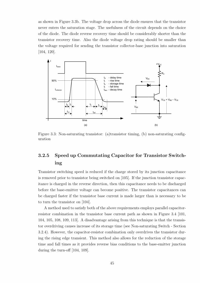
as shown in Figure 3.3b. The voltage drop across the diode ensures that the transistor
never enters the saturation stage. The usefulness of the circuit depends on the choice
of the diode. The diode reverse recovery time should be considerably shorter than the
transistor recovery time. Also the diode voltage drop rating should be smaller than
the voltage required for sending the transistor collector-base junction into saturation
[104, 120].
Figure 3.3: Non-saturating transistor: (a)transistor timing, (b) non-saturating config-uration
3.2.5 Speed up Commutating Capacitor for Transistor Switch-
ing
Transistor switching speed is reduced if the charge stored by its junction capacitance
is removed prior to transistor being switched on [105]. If the junction transistor capac-
itance is charged in the reverse direction, then this capacitance needs to be discharged
before the base-emitter voltage can become positive. The transistor capacitances can
be charged faster if the transistor base current is made larger than is necessary to be
to turn the transistor on [104].
A method used to satisfy both of the above requirements employs parallel capacitor-
resistor combination in the transistor base current path as shown in Figure 3.4 [101,
104, 105, 108, 109, 113]. A disadvantage arising from this technique is that the transis-
tor overdriving causes increase of its storage time (see Non-saturating Switch - Section
3.2.4). However, the capacitor-resistor combination only overdrives the transistor dur-
ing the rising edge transient. This method also allows for the reduction of the storage
time and fall times as it provides reverse bias conditions to the base-emitter junction
during the turn-off [104, 109].
45

Figure 3.4: Speed up capacitor configuration
3.2.6 Shorted Turn - Theory and Application
Faraday’s Law defines the behaviour of an induced voltage in a coil under the influence
of a time-dependent magnetic flux. The induced EMF (ξ) in a circuit is proportional
to the rate of change of magnetic flux (dφ) in that circuit. If the circuit is represented
by a coil of N turns then the induced EMF is given by Equation 3.1.
ξ = −Ndφ
dt(3.1)
Lenszs’ Law dictates that the induced flux generates a voltage (back EMF) that tries
to oppose any change in the circuit. The inductive properties of the magnetic circuit,
defined in Equation 3.2, influence the way in which a time-dependent current flows and
subsequently the magnetic flux it produces. In the case of a simple transformer wound
on a ferromagnetic core, the inductance (L) of the circuit increases with the increase
of the relative permeability (µr) of the material used. The induced output voltage and
the nature of its shape can be controlled by manipulating the way a time-dependent
current establishes a magnetic flux and the way this flux is made to collapse. Hence
the frequency spectrum of the output pulse is also controllable.
L =µrN
2µ0Ac
lc= µrL0 (3.2)
L = N(dφ
di) (3.3)
The coil inductance is also the measure of the change in linking flux as a result of
change of current flow in the coil (Equation 3.3). Equation 3.3 implies that the large
current change with no substantial flux change results in small coil inductance. This
emphasises the importance of the operating point on the hysteresis curve (Figure 3.5).
Operation on the steep slope of the curve results with a substantial coil inductance.
However, if the operating point is in the saturating region or near it, then a large change
in current will cause a very small change in flux and thus the coil inductance will be
significantly lower than in the previous case. Simultaneously, the induced voltage is
46
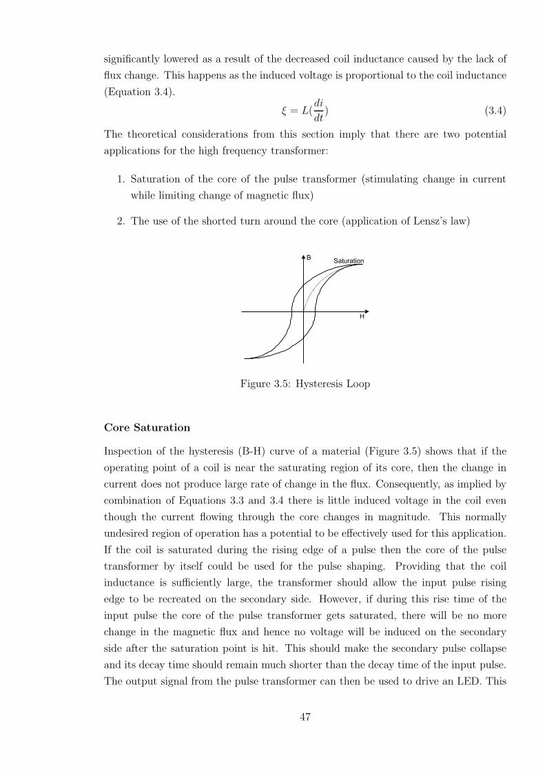
significantly lowered as a result of the decreased coil inductance caused by the lack of
flux change. This happens as the induced voltage is proportional to the coil inductance
(Equation 3.4).
ξ = L(di
dt) (3.4)
The theoretical considerations from this section imply that there are two potential
applications for the high frequency transformer:
1. Saturation of the core of the pulse transformer (stimulating change in current
while limiting change of magnetic flux)
2. The use of the shorted turn around the core (application of Lensz’s law)
Figure 3.5: Hysteresis Loop
Core Saturation
Inspection of the hysteresis (B-H) curve of a material (Figure 3.5) shows that if the
operating point of a coil is near the saturating region of its core, then the change in
current does not produce large rate of change in the flux. Consequently, as implied by
combination of Equations 3.3 and 3.4 there is little induced voltage in the coil even
though the current flowing through the core changes in magnitude. This normally
undesired region of operation has a potential to be effectively used for this application.
If the coil is saturated during the rising edge of a pulse then the core of the pulse
transformer by itself could be used for the pulse shaping. Providing that the coil
inductance is sufficiently large, the transformer should allow the input pulse rising
edge to be recreated on the secondary side. However, if during this rise time of the
input pulse the core of the pulse transformer gets saturated, there will be no more
change in the magnetic flux and hence no voltage will be induced on the secondary
side after the saturation point is hit. This should make the secondary pulse collapse
and its decay time should remain much shorter than the decay time of the input pulse.
The output signal from the pulse transformer can then be used to drive an LED. This
47

technique could potentially reduce the pulse fall time, but does not improve the rise
time. The issue of the rise time would have to be dealt with the use of faster switching
components.
The core required for this application should allow easy saturation as the input
pulses to the transformer in high frequency small signal applications have relatively
small power. Effectively, the amount of current needed to saturate the core should be
relatively low if the above principle is to generate the expected outcome.
The described system is modelled as shown in Figure 3.6. Transfer functions, which
are the mathematical representations of the relationship between the output and input
of a system, can be used to model this dynamic system. The second order transfer func-
tion applied to the unit step generates the input signal by differentiating (numerator)
the input step function and consequently generating the band limited (denominator)
impulse. The tansig (hyperbolic tangent sigmoid transfer function) in combination
with the first order transfer function represent the system. Here, the differentiation
of the input impulse represents the induction of the voltage in the system. The theo-
retical input and its output response are shown in Figure 3.7. The output is reduced
in magnitude, has narrower pulse width and faster turn off than the input pulse. The
negative portion of the output signal is preferred for driving LEDs in this application
for the reasons described in Section 3.3.
Figure 3.6: Core saturation - model
0 1 2 3 4 5 6 7 8 9 10−0.1
−0.05
0
0.05
0.1
0.15
0.2
0.25
0.3
0.35
0.4
Time [ns]
Vol
tage
[V]
input pulseoutput pulse
Figure 3.7: Core saturation model - simulation results
48

Shorted Turn
The shorted turn is commonly used in transformer design for the purpose of active
shielding, especially in very sensitive applications like medical or audio instruments.
The shorted turn is a band of copper that wraps around the core of a transformer. When
used, it acts as an additional secondary winding with very low impedance, capable of
drawing large amount of current. When in operation, as any other secondary winding,
the shorted turn will induce voltage and the current flowing through it will oppose
the flux generated in the coil (Lenz’s law), therefore nulling the original magnetic flux.
The shorted turn increases the rate at which the power dissipates in the circuit, thus
lowering the ’Q’ factor by decreasing the effective inductance [123]. This technique is
regularly implemented for speed control of the magnetic head in data storage equipment
[124]. It is proposed that the same method is explored in the planned pulse shaping
for LED driving.
The above prediction is tested experimentally. The circuit shown in Figure 3.8 is
constructed. The transformer is assembled by winding two coils around a toroid. A
shorted turn is also added to the toroid. This is just a single piece of wire wound
around the core with its ends shorted together.
The circuit (considered in Chapter 6) used to create the pulse is irrelevant as this
is employed only to prove the principle of operation and investigate the possibility of
applying the concept in later stage of the LED driver design. The measurements have
proved that the technique that involves the use of shorted turn can be used to reduce
the time of the falling edge of the pulse. It also reduces the ringing period of the
transformer by approximately factor of ten. The experimental results show that the
effective input impedance of the pulse transformer used later in Chapter 6 is reduced
by up to a factor of hundred using this technique.
Figure 3.8: Shorted Turn test circuit setup
49

3.3 LED Switching Parameters
Due to the finite diffusion time in the semiconductor material the initiation of the
minority carrier injection does not instantly result in a substantial minority carrier
gradient between two sides of the PN junction. This lack of a large differential carrier
concentration limits the flow of diffusion current across the device even though the diode
is in the process of being forward biased. Consequently, the LED initially presents high
resistance to the current flow. As the excess minority carriers drift further from the
junction, the diffusion current increases and the diode resistance falls. The pseudo-
transient resistance is dominant when the device is being turned on (as indicated in
the following paragraph).
The LED releases photons upon initiation of the recombination process. The delay
between an applied electrical pulse and the photonic output is caused by removal of
the capacitance charges, the carrier diffusion and carrier recombination time. Addi-
tionally, the speed at which the LED responds to its driving pulse depends on the
driving current pulse rise time and magnitude [120, 125]. If the LED is not appre-
ciably reverse biased prior to the application of a driving pulse then the effect of the
diode junction capacitance becomes less dominant. This is because the time taken to
charge this capacitance becomes negligible [120]. The LED behaves only as a high
value resistor during the short turn on period while the capacitive effect is eliminated.
During this period the photon producing process is established and the device emits
light. Thereafter the optical output is expected to follow the driving current pulse.
When the electrical signal to the junction is removed the excess minority carriers
near the junction take a finite time to recombine with the majority carriers. This
leads to a natural decay of the optical signal, which is governed by the minority carrier
lifetime. Hence, the excess minority carriers, which are near the junction just before the
removal of the driving signal, are responsible for the exponential turn off decay of the
optical output [90]. The LED continues to generate light through recombination process
until the excess minority carriers are removed. The characteristic time constant of this
decay (see Section 2.2.2), denoted minority carrier lifetime τc, defines LED frequency
response [92] as shown in Equation 3.5 where R(f) is response at a given frequency.
R(f) =R(0)
√
1 + 4π2f 2τ 2c
(3.5)
Equation 3.5 is valid providing that the low-level injection conditions are satisfied. For
high level injection the concept of constant lifetime no longer applies and some average
value of τc must be assumed [92].
An alternative method of analysing the pulse performance of the LED would in-
volve consideration of device’s electrical characteristics. When an ideal electrical pulse
50

is applied to a purely resistive load, the voltage developed across the load is expected
to closely mimic the input signal with respect to time. However, if reactive components
are introduced into the circuit, the response of the complex load modifies the charac-
teristics of the pulse shape. This latter point must be considered when fast changing
electrical signals are used to drive LEDs. When dealing with a device in practice it is
necessary to consider the effects of both the depletion and diffusion capacitances along
with any parasitic impedance attributable to the circuit layout. When the diode starts
to conduct the depletion capacitance disappears due to the removal of the parallel plate
effect. Simultaneously, the carriers injected into the forward biased junction form the
diffusion capacitance. The dynamic electrical impedance presented by the diode during
switching is that of complex voltage dependant impedance, initially dominated by the
depletion capacitive reactance combined with a high valued resistor. At forward bias
voltages the impedance is controlled by the normal diode equation (Equation 2.29) in
combination with LED capacitance. Hence, the parameter that limits the modulation
frequency of an LED is the diffusion capacitance. As this capacitance is dominant
over the junction capacitance in forward bias mode the junction capacitance can be
neglected. Consequently the LED frequency response is dictated by the diffusion capac-
itance. Because this capacitance is the function of minority carrier lifetime (Equation
2.43 with reference to Equations 2.17 and 2.18) it is concluded that the minority carrier
lifetime is the defining parameter for LED frequency response.
It follows from Equation 3.5 that the frequency response of the LED can be in-
creased by reduction of minority carrier lifetime. This can be achieved by introduction
of recombination-generation centres that have energy levels located near the mid-gap
of material forming the p-n junction, such as gold in silicon [96]. Alternative solutions
are use of highly doped active regions [126] or application of heterostructures. Minority
carrier lifetime is reduced in heterostructures by formation of high carrier concentra-
tions within small well regions [96]. Reduction of minority carrier lifetime inevitably
results in decline of LED quantum efficiency. Therefore, this is not a feasible solution
for those applications that require maximum possible optical output. The control of
the minority carrier lifetime is dictated by the manufacturing processes and cannot be
subsequently altered.
In practice, the junction capacitance needs to be taken into account when an elec-
trical pulse is applied to a diode. The junction capacitance affects diode response if not
eliminated or reduced prior to application of the driving pulse. The way to minimise
the effect of this capacitance on diode pulse response is by ensuring the diode is not
reverse biased prior to a pulse being applied to the device.
It is generally considered a good practice to reverse bias the diode immediately after
the positive cycle of the drive pulse is removed in order to sweep out the remaining
excess minority carriers. A bipolar drive pulse is used to achieve this condition. Using
51
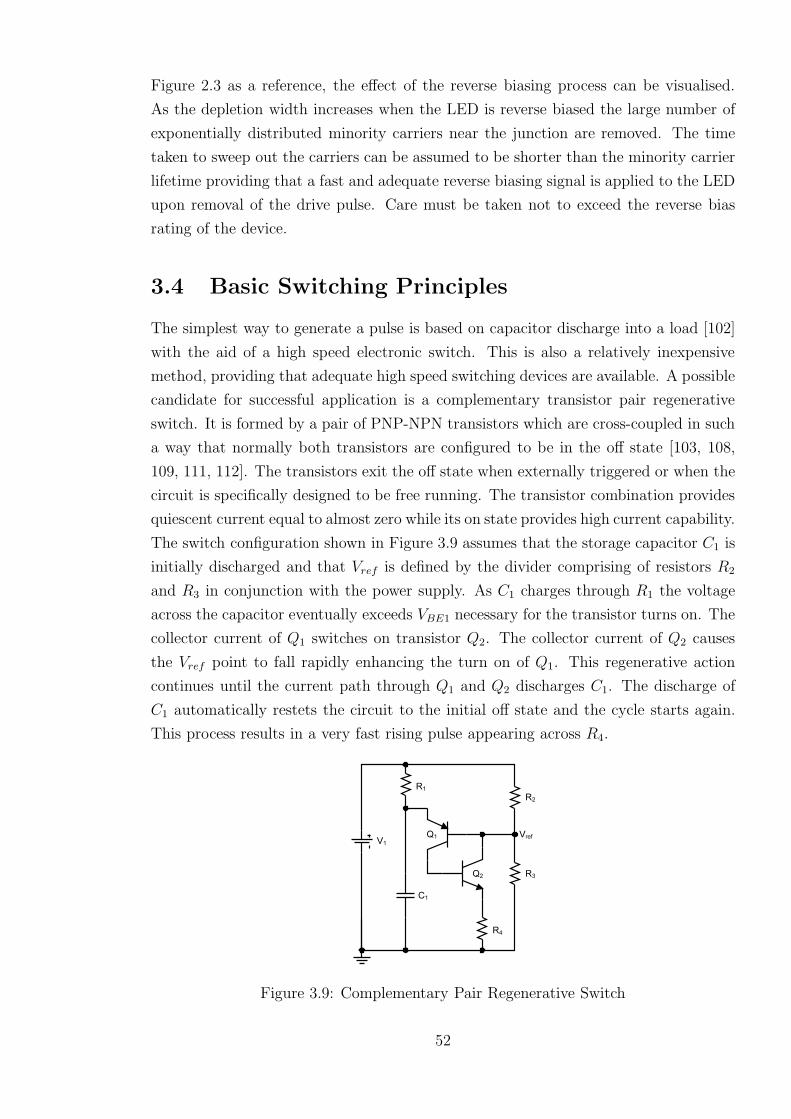
Figure 2.3 as a reference, the effect of the reverse biasing process can be visualised.
As the depletion width increases when the LED is reverse biased the large number of
exponentially distributed minority carriers near the junction are removed. The time
taken to sweep out the carriers can be assumed to be shorter than the minority carrier
lifetime providing that a fast and adequate reverse biasing signal is applied to the LED
upon removal of the drive pulse. Care must be taken not to exceed the reverse bias
rating of the device.
3.4 Basic Switching Principles
The simplest way to generate a pulse is based on capacitor discharge into a load [102]
with the aid of a high speed electronic switch. This is also a relatively inexpensive
method, providing that adequate high speed switching devices are available. A possible
candidate for successful application is a complementary transistor pair regenerative
switch. It is formed by a pair of PNP-NPN transistors which are cross-coupled in such
a way that normally both transistors are configured to be in the off state [103, 108,
109, 111, 112]. The transistors exit the off state when externally triggered or when the
circuit is specifically designed to be free running. The transistor combination provides
quiescent current equal to almost zero while its on state provides high current capability.
The switch configuration shown in Figure 3.9 assumes that the storage capacitor C1 is
initially discharged and that Vref is defined by the divider comprising of resistors R2
and R3 in conjunction with the power supply. As C1 charges through R1 the voltage
across the capacitor eventually exceeds VBE1 necessary for the transistor turns on. The
collector current of Q1 switches on transistor Q2. The collector current of Q2 causes
the Vref point to fall rapidly enhancing the turn on of Q1. This regenerative action
continues until the current path through Q1 and Q2 discharges C1. The discharge of
C1 automatically restets the circuit to the initial off state and the cycle starts again.
This process results in a very fast rising pulse appearing across R4.
Figure 3.9: Complementary Pair Regenerative Switch
52

The simplicity and the fast action of the regenerative switch make it an ideal candi-
date for driving LEDs. The transient nature of the pulse makes it suitable for further
pulse shaping. The above switching circuitry is combined with the pulse shaping tech-
niques of Section 3.2 in order to develop adequate LED drivers (Chapter 6).
3.5 Chapter 3 Summary
The LED transient behaviour and the pulsing circuits suitable for driving the LEDs
were covered in this chapter. When pulsed, an LED should act as a resistor at the
instant when the current starts flowing through. This is why the LED electrical pulse
follows the driving signal - with a sharp rising edge assuming that such is provided
by a driver. If the pulse is maintained, the diode capacitance charges to its final
value. Once this charge is built up, the removal of the driving pulse does not cause
instantaneous disappearance of the diode current. The decay of the diode current after
the withdrawal of the driving signal depends on the diode internal RC constant. Hence,
this decay is exponential, as would be expected from a RC network. The decay can
be reduced if the LED is driven into reverse bias upon removal of the positive pulse.
The experimental considerations of the LED properties from Chapter 2 and from this
chapter are considered in Chapter 5.
The prospective LED pulsing techniques and drivers are also reviewed. The com-
plementary resistor pair regenerative switch oscillator is considered as a most feasible
option for the further development. This decision is prompted by the simplicity and
timing capability of the circuit and is also based on the experimental examination of
the techniques described in this chapter. The other reviewed pulse shaping techniques
are also considered as the possible contributors to an amalgamated design that would
achieve the set objectives. It was experimentally determined that the shorted turn
technique was likely to provide largest advantage in terms of pulse shaping in this case.
The circuit development is described in Chapter 6.
The following chapter (Chapter 4) provides the theoretical basis for the modelling
of the LED characteristics from this chapter and Chapter 2.
53
Chapter 4
LED Modelling
The device modelling is a standard part of the design procedure. The intention in this
case is to use the models as a tool that provides the information necessary to determine
the characteristics of the electrical signal required for generation of the desired optical
output. The modelling is considered from a theoretical perspective in this chapter.
The data obtained from experimental characterisation of the devices’ performance
is used for behavioural description of the devices. The observed characteristics do not
necessarily fully describe the devices. Some device characteristics frequently cannot be
observed directly. Modelling is an analogy formed in order to represent the complete
device behaviour. This analogy allows simulation of device or system behaviour. Con-
sequently, it is possible to predict the system response to a known input. An effective
model should match the performance of the practical configuration it is intended to
represent.
The device models are divided into two groups based on the way they are derived.
The equivalent circuit models are based on the theoretical consideration of device
characteristics. The other group of models are derived empirically from the observation
of the experimental results and the fitting of those results with the model. These are
‘black box’ type models. The external behaviour is seen as a most important feature
of such models. Consecutively the internal physical properties of the devices are often
ignored.
The equivalent circuit models are further divided into d.c. and a.c. models depend-
ing on the frequency of operation. The d.c. models are used for the low frequencies
(usually up to 10kHz). The rest of the frequency spectrum is covered by the a.c.
models. These account for parameters such as parasitic capacitances and inductances.
The dependency of the devices on input signal level is represented by the use of
small and large signal models. The small signal models are utilised for the use in the
circumstances where the change in circuit voltages and currents should only cause small
alterations from the d.c.-bias operating point. These models are linearised portions of
the complete device so that the incremental current is proportional to the incremental
54

voltage for the small change around the point of operation. The large signal models are
designed to operate under conditions where input signals cause large variations in the
device operating conditions. The non-linear behaviour of the active devices makes it
particularly difficult to devise an accurate large signal model. Hence these are usually
derived from the analytical expressions or from the empirical relationships fitted to the
experimental data [127].
The types of the device models are shown in Figure 4.1.
Figure 4.1: Types of models
4.1 OrCAD Models
The standard OrCAD (PSPICE) diode models are based on the theoretical considera-
tions of the diode characteristics. The specific models are defined by the user-selected
parameters. These parameters are derived theoretically. Such approach results in the-
oretical definition of the model that might not accurately resemble the performance of
the practical device. Hence, in this case, the experimentally derived diode characteris-
tics are used for definition of the model parameters. The resulting model should be a
closer depiction of the real, rather than the theoretical, device.
PSPICE diode parameters (see appendix B), which define the diode models, are
the standard component of the OrCAD package. The parameter selection used for
definition of a model simultaneously defines the type of model used. The fewer the
parameters used, the less accurate the model is when compared to its equivalent real
device. However, inclusion of the particular parameters is not necessary in every ap-
plication. The type of the application defines the complexity of the model. There is
no need for the use of a large signal a.c. model if the diode is only to operate under
the small signal d.c. conditions.
4.1.1 Ideal Diode Static Model
The ideal diode model is based around the ability to accurately represent the ideal
diode current (Equation 2.29). The PSPICE performs this independently for two bias
55

conditions. Hence, the PSPICE form of the equation is of the form shown in table 4.1.
PSPICE equivalent equation condition
I = Is(eqVkT − 1) + V ∗ GMIN for V ≥ −5kT
qFwd bias & Rev bias
for V ≥ V thermal
I = −Is + V ∗ GMIN for V < −5kTq
Reverse bias
for V < V thermal
Table 4.1: Ideal diode static model current
It should be noted that GMIN in table 4.1 is added by default in parallel with
every p-n junction. Its default value is 10-12S and it cannot be set to zero. It is
not important in terms of the diode characteristic description as it is a program (not
device) parameter and is added to enhance computational efficiency. It also does not
show any observable influence on the diode characteristic [121, pp160].
The saturation current (Is) is of opposite polarity from that of I. However, the
measured value of the saturation current is considered by PSPICE as −Is, hence the
negation symbol in the relationship between the diode current and saturation current
is dropped out.
The d.c. forward characteristic in the PSPICE equation is determined by the satu-
ration current only. However, Is is a constant in SPICE and as such does not properly
model the voltage dependence of the depletion region current, which is due to the
varying width of the depletion region. The complexity of the model increases for closer
depiction of the real device.
4.1.2 Real Diode Static Model
Even though the experimental results for most junction diodes show a range of charac-
teristics which are in agreement with the ideal diode equation, some discrepancies are
present due to [93]:
• Carrier generation-recombination in the depletion layer
• High level injection
• Voltage drop associated with the electric field in the neutral regions
• Internal breakdown associated with high reverse voltage
The combination of these mechanisms results in more realistic diode models. De-
pending on which of the above mechanisms is considered during the modelling process,
three different model types of the real diode are generated.
56
Real Diode: Small Bias - Effect of the Carrier Recombination-Generation
Idealised diode models assume constant electron and hole currents through deple-
tion region [93]. The effect of this assumption is that the actions of the generation-
recombination centres in the depletion region are ignored. Under forward bias condi-
tions these centres contribute to the recombination process. Also when the depletion
region is reverse biased, these centres act as source of free carriers. The effect of these
two actions on the diode overall current is usually minimal. However, the activity of
these centres needs to be considered when creating a precise model.
If the total current of a real diode (taking account of generation − recombination
process) is given by Equation 4.1, where ID(ideal) is the ideal diode current and I(r,g)
is the current caused by the generation-recombination process, then the current un-
der reverse bias of the diode is generated predominantly in the depletion region. The
current in the forward biased diode is dominated by the ideal diode diffusion current,
especially as bias increases. In general, an expression that well describes the effects
due to the generation-recombination processes is given by the empirical relation shown
in Equation 4.2 where η, the emission coefficient, is usually about 2 if the recombi-
nation current dominates and is equal to 1 for the ideal diode behaviour [93]. The
ideality factor (in PSPICE emission coefficient) η is the component introduced in the
representation of the real diode - Equation 2.30. Equation 4.2 is an equivalent of Equa-
tion 2.29, but with the added ideality factor which takes into account the effect of the
generation-recombination centres in the depletion layer. It is also a simplified version
of the practical diode equation (Equation 2.30); it ignores the voltage drop across the
diode series resistance and the current flow through the diode parallel resistance.
ID = ID(ideal) + I(r,g) (4.1)
I = Is
[
exp
(
qV
ηkT
)
− 1
]
(4.2)
The graphical representation of the electric components used to represent the small bias
real diode model is shown in Figure 4.2a. The diode parasitic elements are ignored and
the model relies purely on diode equation. The PSPICE form of the diode equation
used for this model is shown in table 4.2.
PSPICE equivalent equation condition
I = Is(eqVηkT − 1) + V ∗ GMIN for V ≥ −5ηkT
qFwd bias & Rev bias
for V ≥ V thermal
I = −Is + V ∗ GMIN for V < −5ηkTq
Reverse bias
for V < V thermal
Table 4.2: Small bias current of the real diode model
57
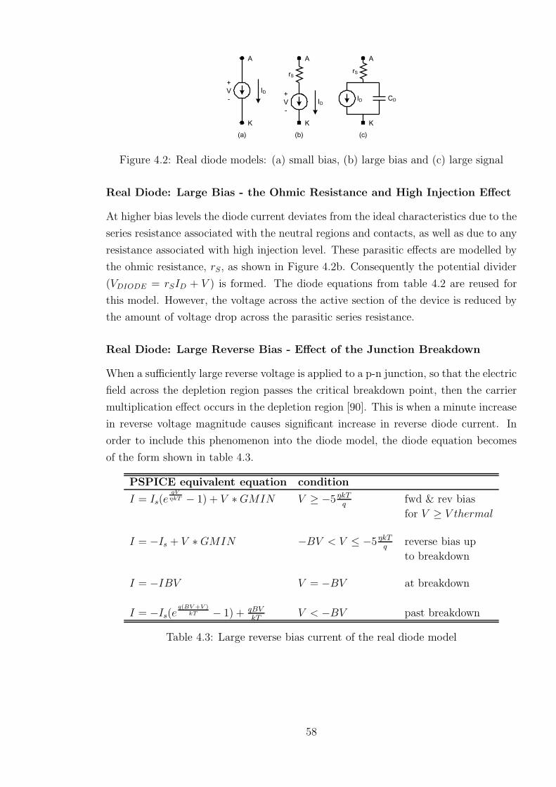
Figure 4.2: Real diode models: (a) small bias, (b) large bias and (c) large signal
Real Diode: Large Bias - the Ohmic Resistance and High Injection Effect
At higher bias levels the diode current deviates from the ideal characteristics due to the
series resistance associated with the neutral regions and contacts, as well as due to any
resistance associated with high injection level. These parasitic effects are modelled by
the ohmic resistance, rS, as shown in Figure 4.2b. Consequently the potential divider
(VDIODE = rSID + V ) is formed. The diode equations from table 4.2 are reused for
this model. However, the voltage across the active section of the device is reduced by
the amount of voltage drop across the parasitic series resistance.
Real Diode: Large Reverse Bias - Effect of the Junction Breakdown
When a sufficiently large reverse voltage is applied to a p-n junction, so that the electric
field across the depletion region passes the critical breakdown point, then the carrier
multiplication effect occurs in the depletion region [90]. This is when a minute increase
in reverse voltage magnitude causes significant increase in reverse diode current. In
order to include this phenomenon into the diode model, the diode equation becomes
of the form shown in table 4.3.
PSPICE equivalent equation condition
I = Is(eqV
ηkT − 1) + V ∗ GMIN V ≥ −5ηkTq
fwd & rev bias
for V ≥ V thermal
I = −Is + V ∗ GMIN −BV < V ≤ −5ηkTq
reverse bias up
to breakdown
I = −IBV V = −BV at breakdown
I = −Is(eq(BV +V )
kT − 1) + qBVkT
V < −BV past breakdown
Table 4.3: Large reverse bias current of the real diode model
58

4.1.3 Large Signal Model
The small signal model with its linearised portions of the diode characteristics is not
suitable for simulation where input signals cause large variations in the operating con-
ditions. Consequently, a large signal model is used in order to allow the observation of
the diode behaviour in a variety of circumstances.
The key aspect of the large signal diode models is charge storage. If there was
no charge storage, the devices would be infinitely fast as there would be no charge
inertia and the currents could be changed in zero time [93, pp19] (see ’Capacitance
- Voltage relationship’ in Section 2.2.3). The charge storage in the depletion region
due to concentration of the doping atoms and charge storage due to minority carrier
charges injected into the neutral regions are shown in Equations 4.3 and 4.4 [90, 93].
Qj =
√
2qεS(vbi − V )1
NA+ 1
ND
(4.3)
Qd = (Qn + Qp) = τDID (4.4)
The stored charge Qn and Qp are defined in Equations 2.40 and 2.41. Combining the
Equation 2.32 with the Equations 4.3 and 4.4 the PSPICE proffered versions of the
diode capacitances can be derived - Equations 4.5 and 4.6.
Cj =dQj
dV=
Cj(0)√
1 − VVbi
(4.5)
Cd =dQd
dV=
q
ηkTτDISe
qVηkT (4.6)
For reverse bias and small forward bias Qj is the dominant charge storage. For mod-
erate forward bias and beyond the injected charge Qd dominates [93]. The crossover
of the two types of capacitance dominant behaviours occurs at the low level forward
bias. The Equation 4.5 becomes invalid as the voltage across the junction approaches
the built in potential. At this point the charge stored in the depletion region is non
existent (see Equation 4.3) driving the junction capacitance into theoretical infinity.
The diode capacitance is the sum of the two capacitances (Equation 4.7).
CD = Cj + Cd =d(Qj + Qd)
dV=
dQD
dV(4.7)
Thus the diode large signal can be represented as in Figure 4.2c. The stored charges
Qj and Qd that are of the main interest for calculations of the diode capacitance. The
PSPICE definition of the stored charge is shown in table 4.4.
where F1, F2 and F3 are SPICE constants determined by the coefficient for the
forward bias depletion capacitance formula (FC) and grading coefficient (m) [93] and
59

QD= Qd +Qj condition
QD = τDID +Cj(0)VD∫
0
(1 − Vvbi
)−mdV for VD < FC ∗ vbi
QD = τDID +Cj(0)F1 +Cj(0)
F2
VD∫
FC∗vbi
(F3 + mVvbi
)dV for VD > FC ∗ vbi
Table 4.4: PSPICE stored charge definition
are defined as:
F1 = vbi
1−m(1 − FC)(1+m) , F2 = (1 − FC)1+m and F3 = 1 − FC(1 + m)
As the capacitance is defined as rate of change of charge with respect to voltage
change (Equations 4.5 and 4.6), the above charge definitions results with the PSPICE
charge characterisations as shown in table 4.5.
CD=dQD
dV= Cd +Cj condition
CD = τDdID
dV+Cj(0)(1 − V
vbi)−m for V < FCvbi
CD = τDdID
dV+
Cj(0)
F2(F3 − mV
vbi) for V > FCvbi
Table 4.5: PSPICE diode capacitance
with m being equal to 0.33 for a linearly graded junction or 0.5 for an abrupt
junction and FC being a factor between 0 and 1. FC determines the way in which the
junction capacitance is calculated when the diode is forward biased. This is required
because of the collapse of the theoretical approximation of the junction capacitance as
the forward bias voltage approaches the built in junction potential value [93, pp23]. The
PSPICE equivalent parameter names for the above equations are shown in appendix
B.
4.2 Behavioural Models
The behavioural models are based on the information obtained from experimental
observations of LED external behaviour. The proposed relationships between measured
variables are confirmed through data analysis (curve fitting). This process yields a set
of simple parameters that are consequently used to mimic the established relationships.
The amalgamation of a mixture of relationships into an effective unit corresponds to a
behavioural model of a device.
Instead of relying on limited standard diode models, the purpose built behavioural
models can be created. The models are based on the experimentally obtained rela-
tionships between diode current and voltage, capacitance and voltage and current and
light intensity. The electrical characteristics of the models are based on the diagram
60

shown in Figure 4.3. Equation 2.30, derived from this Figure, is used to represent the
steady state current flow through the device. The parasitic capacitances are consid-
ered for the purpose of predicting the device transient response. It is assumed that
the capacitive current does not contribute to the light generation. This assumption is
not important when considering the steady state current flow. However, the capacitive
current is an important factor when considering the frequency response of the devices.
Consequently, large ratio between capacitive and resistive currents can limit or even
prevent the fast generation of light.
Figure 4.3: Complete practical diode model
The LED optical properties are derived from the experimentally determined cur-
rent – light intensity relationship. As this relationship is established at steady state
conditions it is assumed that the measured current is purely resistive. Therefore, it is
assumed that this relationship relates to the resistive current, not device current, even
at higher switching speeds when the capacitive current is present.
The model was derived with use of the generally accepted theoretical relationships
(Section 2.2). The model parameters are obtained from the curve fittings (described
in Section 5.1). The encountered discrepancies between the experimental findings and
anticipated theoretical predictions are incorporated into the relationships so that the
model evolves accordingly (Section 5.2). The plausible explanations for the discrepan-
cies are sought.
4.3 Chapter 4 Summary
The methods of modelling LEDs were covered in this chapter. These include the stan-
dard PSPICE models and the custom built behavioural models. The model parameters
are derived from the experimentally determined relationships (Section 5.1). The ac-
quired set of parameters is incorporated into mathematical expressions defined by the
final established relationships between the observed variables. The theoretical expres-
sions for the LED characteristics (Section 2.2) were altered to fit the experimentally
obtained data. Hence, the models are orientated towards the practical devices as op-
posed to their theoretical predictions. These are practically realised in OrCAD and
MATLAB software packages. The obtained models are dealt with in Section 5.2.
61

Chapter 5
Experimental and Modelled LED
Characteristics
Even though the shape of the LED output pulses is generally governed by the driving
signal it is also restricted by the LED characteristics. This is especially the case at
higher frequencies as instantaneous switching between the on and off states is not
possible to achieve (see Section 3.3). It is the importance of the transient response
of the LEDs that has prompted the need for experimental determination of the LED
characteristics. The LEDs used in this case are Agilent HLMP-CB15 [128]. These
devices have been used in the ANTARES project. They have proved to be the most
suitable components available on the market at the time when the ANTARES LED
drivers were built. It was decided to continue developing the drivers for the same
devices so that any potential improvements can be directly compared to the previous
work of the same type.
Section 5.1 looks at the electrical and optical characteristics of the chosen LEDs.
These characteristics are relevant for the pulsing operation of the chosen devices. The
identified deviations of the experimental characteristics from the theoretically antic-
ipated relationships are analysed. Consequent hypothetical explanations for the dis-
covered differences are presented in this section. Possible effects of the unexpected
properties are considered.
Section 5.2 concentrates on generation of LED models based on the experimental
findings. Three types of models are generated and their characteristics are compared.
5.1 Methods and Results
The LED characteristics that were found most dominant for the application are tested.
The importance of device capacitance for switching characteristics prompted the mea-
surement of the capacitance - voltage relationship. The somewhat indistinct current -
62

voltage relationship from the manufacturer’s data sheet prompted check of this char-
acteristic. The LED output spectrum followed in an attempt to describe certain dis-
crepancies occurring in the previous measurements on the LEDs. A less common de-
termination of LED photo-detection characteristics was conducted amid the attempts
to explain the unexpected abnormalities occurring in the other LED characteristics.
Two groups of the LEDs are tested. They are of the same type [128] and are
obtained from the same source (FarnellInOne) at two different occasions. It is not
known if the LEDs from a group come from the same manufacturing batch. In order to
distinguish between the two, the groups are named BATCH-1 and BATCH-2 further
in the text. Each batch contains twenty LEDs and they are labelled numerically from
1 to 40.
5.1.1 Capacitance - Voltage Relationship
The importance of the capacitance in LED switching was described in Section 3.3.
Consequently the capacitance – voltage relationship is deemed an important charac-
teristic that needs to be determined. The measurements of the internal LED capac-
itance with respect to the changing voltage across the LED were performed using a
Marconi TF1313 Universal Bridge [129]. The voltage is applied with an external bias
circuitry – constructed as shown in Figure 5.1. The available measuring frequencies
are 1kHz and 10kHz. All the capacitance measurements are obtained at 1kHz as this
frequency offers improved measurement accuracy [129]. The LED under test forms
a part of the bridge as shown in Figure 5.2. The capacitance reading is taken once
the currents flowing through different branches of the bridge are balanced using the
external controls. The reading represents the capacitance of the device (including the
possible package parasitic capacitance). The effect of the parasitic lead capacitance is
established to constitute a negligible portion of the total reading. The maximum value
of the parasitic capacitance contributes to the total capacitance reading in order of less
than 0.34%. The lead parasitic capacitance can be established by physically cutting
the top end of the LED enclosure and breaking off the junction prior to capacitance
measurement of the remainder of the device.
Figure 5.1: Marconi TF1313 bridge bias circuit
63

Figure 5.2: Simplified TF 1313A Bridge Diagram
The external bridge bias circuit (Figure 5.1) is constructed in order to extend the
bias range for the capacitance measurement. A standard biasing circuit delivers output
necessary for reverse bias only (−4.5V to −1.5V ). Even though the biasing circuit
provides swing from −4.5V to 4.5V it is not possible to measure LED capacitance above
2V bias with this arrangement because of dramatic increase in diffusion capacitance
above this bias level. The exponential increase of the current flowing through the
device makes it impossible to keep the test bridge balanced because of the exponential
rise of the diffusion capacitance.
The effect of the changing d.c. bias on the bridge can be investigated in order to
establish if the measurements are affected by the bias alterations. This effect is verified
with the d.c. bias circuit supplying current while no LED is present in the bridge.
The maximum change in current provided to the bridge for the voltage supply swing
from −4.5V to 4.5V is 20nA. The possible error introduced by this phenomenon is
insignificant.
The above measurement procedure is performed on two batches of the LEDs (see
Section 5.1). The results are expected to follow the LED behaviour described in Chap-
ter 2.2.3. That is, the capacitance behaviour should follow the relationship from Equa-
tion 2.36 (and consequently Equation 2.37) at reverse bias voltages and its trend should
be a mixture of the relationship from Equations 2.36 and 2.43 in forward bias region.
The exponential behaviour from Equation 2.43 should become dominant at larger for-
ward biases when diffusion capacitance takes over and the junction capacitance van-
ishes (see Chapter 2.2.3). The experimentally determined C-V relationship is shown
in Figure 5.3.
A number of discrepancies between the measured and theoretical C-V relationships
is evident from examination of the graphical data (Figure 5.3). The internal capaci-
tance for two LEDs (labelled 39 and 40) is significantly higher that that of the rest of
the LEDs, even though their shape is generally comparable. Closer inspection of the
remainder of the curves shows a distinctive difference between the curves belonging
to two different batches, as shown in Figure 5.4 (the LEDs 38, 39 and 40 are omitted
from Figure 5.4b). There are also two distinguishable groups of the curves exhibited
by the LEDs in BATCH-1 (Figure 5.4a). There are six curves in BATCH-1 C-V char-
64
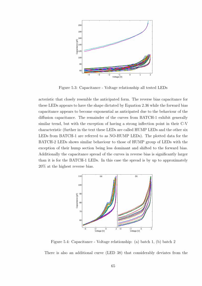
−4 −3 −2 −1 0 1 2
60
80
100
120
140
160
180
200
Voltage [V]C
apac
itanc
e [p
F]
Figure 5.3: Capacitance - Voltage relationship all tested LEDs
acteristic that closely resemble the anticipated form. The reverse bias capacitance for
these LEDs appears to have the shape dictated by Equation 2.36 while the forward bias
capacitance appears to become exponential as anticipated due to the behaviour of the
diffusion capacitance. The remainder of the curves from BATCH-1 exhibit generally
similar trend, but with the exception of having a strong inflection point in their C-V
characteristic (further in the text these LEDs are called HUMP LEDs and the other six
LEDs from BATCH-1 are referred to as NO-HUMP LEDs). The plotted data for the
BATCH-2 LEDs shows similar behaviour to those of HUMP group of LEDs with the
exception of their hump section being less dominant and shifted to the forward bias.
Additionally the capacitance spread of the curves in reverse bias is significantly larger
than it is for the BATCH-1 LEDs. In this case the spread is by up to approximately
20% at the highest reverse bias.
−4 −2 0 2
60
70
80
90
100
110
Voltage [V]
Cap
acita
nce
[pF
]
(a)
−4 −2 0 2Voltage [V]
(b)
Figure 5.4: Capacitance - Voltage relationship: (a) batch 1, (b) batch 2
There is also an additional curve (LED 38) that considerably deviates from the
65

general shape adopted by the remainder of the curves (as shown in Figure 5.5).
−4 −3 −2 −1 0 1 2
60
70
80
90
100
110
Voltage [V]
Cap
acita
nce
[pF
]
LED38LEDs 21−37
Figure 5.5: Capacitance - Voltage relationship: LEDs 21 - 38
A standard way of representing C-V characteristic is by plotting inverse of the
capacitance squared versus voltage (Equation 2.37). As it is only the reverse bias
condition that is normally considered, the commonly displayed capacitance is depletion
capacitance. Such plot allows extrapolation of LED impurity concentration. This
method is not used in this case, but the relevant plot is shown for reference purposes
in appendix C.1. It should be noted that the biasing arrangement for the capacitance
measurement in this case yields a combination of depletion and diffusion capacitance.
The capacitance is tested over the extended bias with the aim of describing the complete
behaviour of the LEDs over a range of conditions. It was considered that the diffusion
capacitance ought to be included into such investigation. It was also discovered that
the understanding of the capacitance behaviour in the low forward bias is not definite.
The available models are scarce and slightly ambiguous when it comes to the transfer
of dominance from the depletion to the diffusion capacitance at the low forward bias
[93]. Hence, an attempt was made to investigate capacitance in this region.
The above analysis is a product of graphical data observations and hence is not
exact enough to provide unambiguous conclusions about the discrepancies between the
theoretical and practical LED characteristics. The data is therefore analysed further.
From the measurement of the parasitic capacitance (described earlier in this section)
it is concluded that this capacitance could not generate such a significant discrepancy
between theoretical and practical LED capacitance. Consequently, the parasitic effect is
ignored in this analysis. It is assumed that the depletion capacitance is the only relevant
contributor to the LED reverse bias capacitance. The combination of the depletion
and diffusion capacitances in forward bias generates the LED total capacitance. It
follows that the discrepancy between the theory and practice must be a product of
one or both of the capacitive components. In order to investigate the reasons for the
66

unexpected LED capacitance behaviour the capacitive components are reconstructed
following the theoretical predictions and fitted to the experimental data. That is, the
diode capacitance behaviour (see Section 2.2.3) is modelled and fitted to the measured
data. The depletion capacitance is constructed using the relationship from Equation
2.37 and fitted to the measured data (see appendix C.2). The depletion capacitance
model values are then subtracted from the measured data and an exponential function
representing diffusion capacitance is fitted to the remainder (see appendix C.3). The
model of the diffusion capacitance is then subtracted from the first remainder and the
second remainder is generated. The shape of the final remainder resembles Gaussian
distribution curve and this distribution is found to be adequate for the model (see
appendix C.4). The three capacitive components are then added together to form the
LED capacitance model (Figures 5.6 - 5.10). The difference between the models and
the data is the fitting error shown in appendix C.5.
The above fitting is performed in MATLAB using its unconstrained nonlinear op-
timization function (fminsearch). It is based on a simplex search method where the
stepwise progress is achieved from one feasible solution to another in such a way that
the value of the fitting function increases [130]. The initial step is defined by the initial
values. The following points depend on the optimality test, which results in a location
of possible better feasible solutions [130]. If such location is available, the transition to
the new point is completed. The simplex search method specific to MATLAB is defined
by Lagarias et al. [131]. The comparison of the function values for the new and the old
point results in a substitution of the point that is further away from the fitting data.
Subsequent points generate the new simplexes. The procedure is reiterated until the
diameter of the simplex falls within the specified tolerance level.
−4 −3 −2 −1 0 1 2
60
70
80
90
100
110
Voltage [V]
Cap
acita
nce
[pF
]
Figure 5.6: Capacitance modelling for NO-HUMP LEDs: *** measured data, model
The main unexpected feature that appears in the measured LED C-V relationship
is the hump feature that appears in some of the tested LEDs. A conclusion from
67
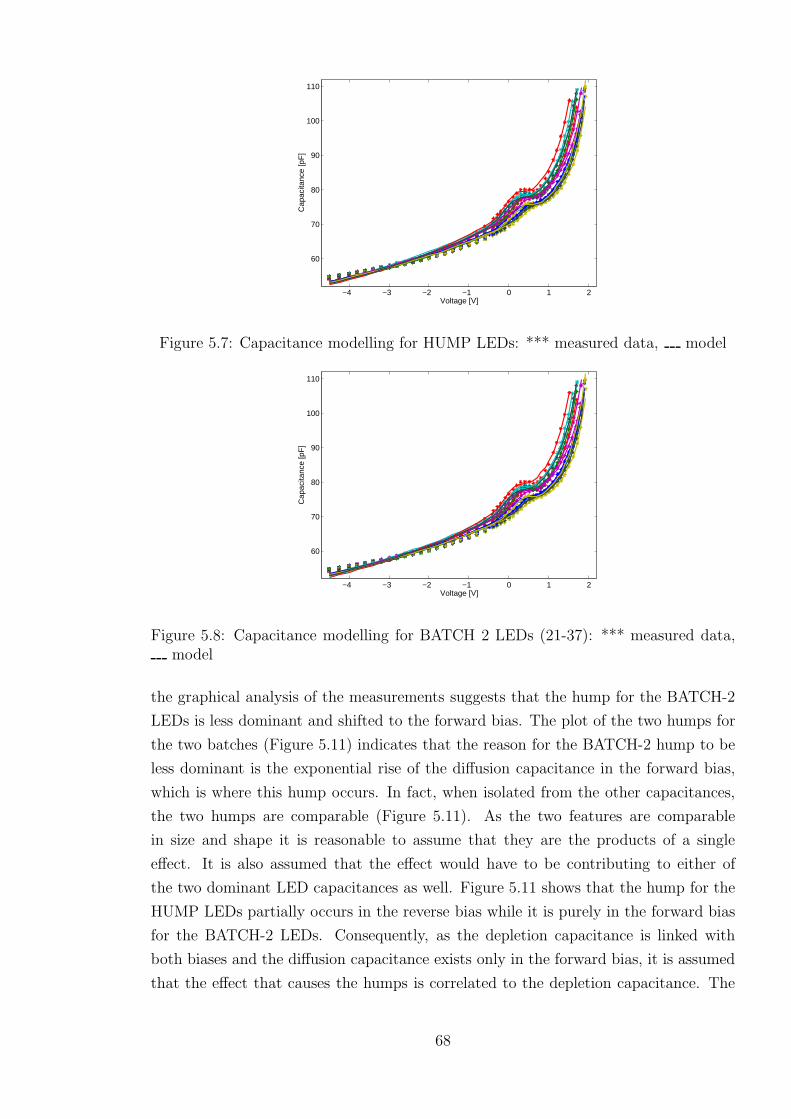
−4 −3 −2 −1 0 1 2
60
70
80
90
100
110
Voltage [V]C
apac
itanc
e [p
F]
Figure 5.7: Capacitance modelling for HUMP LEDs: *** measured data, model
−4 −3 −2 −1 0 1 2
60
70
80
90
100
110
Voltage [V]
Cap
acita
nce
[pF
]
Figure 5.8: Capacitance modelling for BATCH 2 LEDs (21-37): *** measured data,model
the graphical analysis of the measurements suggests that the hump for the BATCH-2
LEDs is less dominant and shifted to the forward bias. The plot of the two humps for
the two batches (Figure 5.11) indicates that the reason for the BATCH-2 hump to be
less dominant is the exponential rise of the diffusion capacitance in the forward bias,
which is where this hump occurs. In fact, when isolated from the other capacitances,
the two humps are comparable (Figure 5.11). As the two features are comparable
in size and shape it is reasonable to assume that they are the products of a single
effect. It is also assumed that the effect would have to be contributing to either of
the two dominant LED capacitances as well. Figure 5.11 shows that the hump for the
HUMP LEDs partially occurs in the reverse bias while it is purely in the forward bias
for the BATCH-2 LEDs. Consequently, as the depletion capacitance is linked with
both biases and the diffusion capacitance exists only in the forward bias, it is assumed
that the effect that causes the humps is correlated to the depletion capacitance. The
68
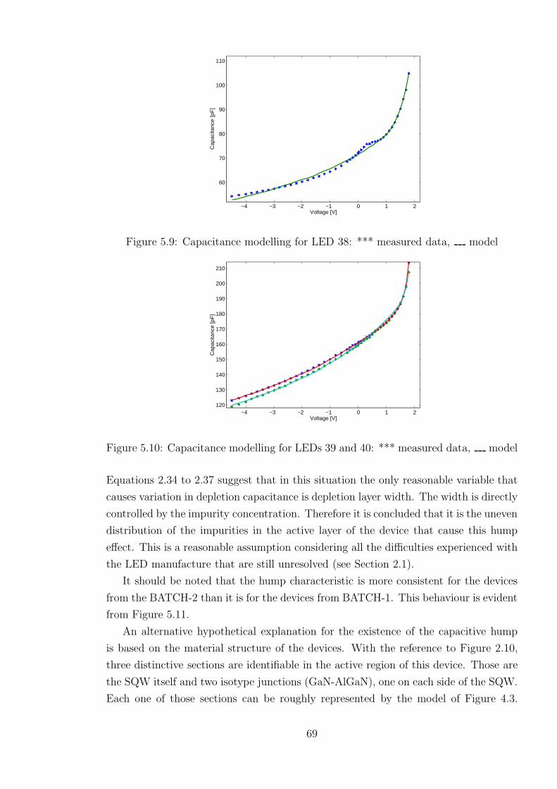
−4 −3 −2 −1 0 1 2
60
70
80
90
100
110
Voltage [V]C
apac
itanc
e [p
F]
Figure 5.9: Capacitance modelling for LED 38: *** measured data, model
−4 −3 −2 −1 0 1 2120
130
140
150
160
170
180
190
200
210
Voltage [V]
Cap
acita
nce
[pF
]
Figure 5.10: Capacitance modelling for LEDs 39 and 40: *** measured data, model
Equations 2.34 to 2.37 suggest that in this situation the only reasonable variable that
causes variation in depletion capacitance is depletion layer width. The width is directly
controlled by the impurity concentration. Therefore it is concluded that it is the uneven
distribution of the impurities in the active layer of the device that cause this hump
effect. This is a reasonable assumption considering all the difficulties experienced with
the LED manufacture that are still unresolved (see Section 2.1).
It should be noted that the hump characteristic is more consistent for the devices
from the BATCH-2 than it is for the devices from BATCH-1. This behaviour is evident
from Figure 5.11.
An alternative hypothetical explanation for the existence of the capacitive hump
is based on the material structure of the devices. With the reference to Figure 2.10,
three distinctive sections are identifiable in the active region of this device. Those are
the SQW itself and two isotype junctions (GaN-AlGaN), one on each side of the SQW.
Each one of those sections can be roughly represented by the model of Figure 4.3.
69

−1 −0.5 0 0.5 1 1.5 2
0
0.5
1
1.5
2
2.5
3
3.5
Voltage [V]C
apac
itanc
e [p
F]
Figure 5.11: Capacitive hump comparison: . HUMP, BATCH 2 (LEDs 21 to 37)
When the device is reverse biased its current source, the series resistance and the diffu-
sion capacitance can be neglected. Therefore the structure is electrically characterised
by a RC network as the identified sections are connected in series. The complexity
of the model increases if the junctions are to be accurately represented. The isotype
junctions can be modelled as back-to-back diodes and consequently each of those is
shown as a series connection of two parallel resistor-capacitor combinations [132]. The
SQW is modelled as a series capacitive network with an additional parallel capacitance
[133]. If taken in very simple terms, the device consists of three capacitive sections.
Each one of those should contain certain amount of depletion capacitance when the
device is reverse biased. As the bias approaches zero voltage the two side capacitances
are potentially likely to colapse earlier than the SQW capacitance. This means that
these two side capacitances would increase in value (to theoretical infinity) and then
suddenly collapse as their local depletion capacitance disappears and the local diffusion
capacitance becomes dominant. This type of effect could theoretically generate the ob-
served local maxima in the capacitance of the complete device. If so, this hypothetical
analysis further confirms that the existence of the humps is generated by the depletion
capacitance.
The importance of the LED capacitance can be further emphasised by the observa-
tion of the optical output generated by the devices with different capacitive character-
istics. It is established that the LEDs with significantly increased internal capacitance
(numbered 39 and 40) generate similar fast switching optical pulses as the other de-
vices, but they need higher driving voltage in order to generate fast switching light.
The required increase in driving signal voltage is in order of 26% to 28%. The irreg-
ularities in the capacitive properties could potentially prevent the generation of fast
switching light. (The findings are generated using the circuits from Chapter 6).
70

5.1.2 Current - voltage relationship
Measurement of the LED I-V characteristic was performed indirectly by measuring the
voltage drops across the LED and across a series resistor (Figure 5.12). The voltage
drop across the series resistor is converted into current flowing through the LED.
Figure 5.12: I-V characteristic - experimental setup
The experimentally determined I-V characteristic is shown in Figure 5.13. The
same is shown on logarithmic scale in Figure 5.14. The graphical data in Figure
5.13 shows reduced current flow through the LEDs from BATCH-1 at higher voltages.
Additionally, the low bias behaviour (Figure D.1 – appendix D) depicts the differences
between the three groups of LEDs. The NO-HUMP group conducts the lowest amount
of current for a given low-level voltage. This is followed by the HUMP LEDs. The
current flowing through the BATCH-2 LEDs for the same voltage level is significantly
higher. This can be seen in Figure 5.14, but is clearer when shown on linear scale up
to a fixed bias voltage point (Figure D.1).
0 0.5 1 1.5 2 2.5 3 3.5 40
10
20
30
40
50
0
10
20
30
40
Voltage [V]
Cur
rent
[mA
]
*** BATCH1
__ BATCH2
Figure 5.13: LED I-V relationship
The comparison of the two logarithmic scale relationships would suggest irregular
behaviour of the LEDs. Assuming that the LED current is exponential, the logarithmic
scale of this relationship should generate a linear graph. However, two very distinct
knees are evident. These can be explained by considering the practical blue LED char-
acteristics (Equation 2.30). The mathematical analysis of the equation (appendix A.2)
71
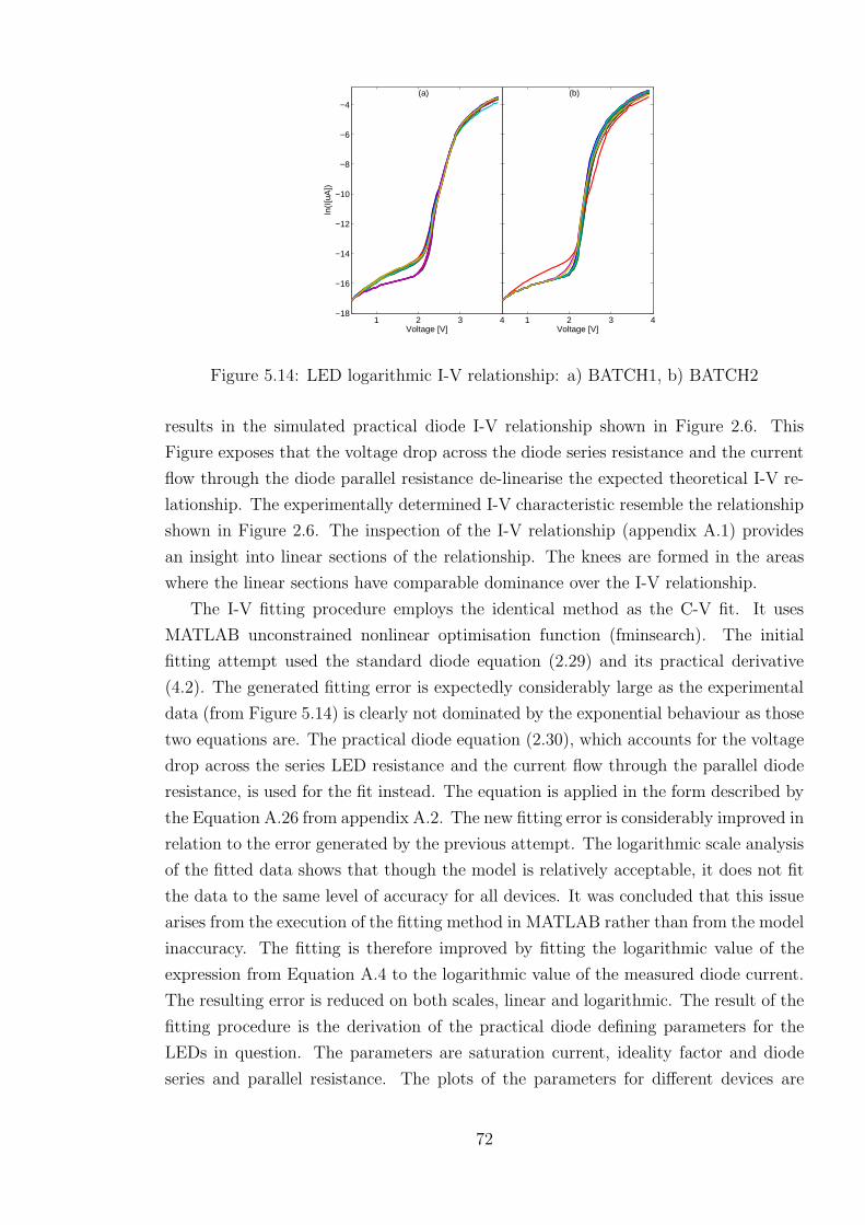
1 2 3 4−18
−16
−14
−12
−10
−8
−6
−4
Voltage [V]ln
(I[u
A])
(a)
1 2 3 4Voltage [V]
(b)
Figure 5.14: LED logarithmic I-V relationship: a) BATCH1, b) BATCH2
results in the simulated practical diode I-V relationship shown in Figure 2.6. This
Figure exposes that the voltage drop across the diode series resistance and the current
flow through the diode parallel resistance de-linearise the expected theoretical I-V re-
lationship. The experimentally determined I-V characteristic resemble the relationship
shown in Figure 2.6. The inspection of the I-V relationship (appendix A.1) provides
an insight into linear sections of the relationship. The knees are formed in the areas
where the linear sections have comparable dominance over the I-V relationship.
The I-V fitting procedure employs the identical method as the C-V fit. It uses
MATLAB unconstrained nonlinear optimisation function (fminsearch). The initial
fitting attempt used the standard diode equation (2.29) and its practical derivative
(4.2). The generated fitting error is expectedly considerably large as the experimental
data (from Figure 5.14) is clearly not dominated by the exponential behaviour as those
two equations are. The practical diode equation (2.30), which accounts for the voltage
drop across the series LED resistance and the current flow through the parallel diode
resistance, is used for the fit instead. The equation is applied in the form described by
the Equation A.26 from appendix A.2. The new fitting error is considerably improved in
relation to the error generated by the previous attempt. The logarithmic scale analysis
of the fitted data shows that though the model is relatively acceptable, it does not fit
the data to the same level of accuracy for all devices. It was concluded that this issue
arises from the execution of the fitting method in MATLAB rather than from the model
inaccuracy. The fitting is therefore improved by fitting the logarithmic value of the
expression from Equation A.4 to the logarithmic value of the measured diode current.
The resulting error is reduced on both scales, linear and logarithmic. The result of the
fitting procedure is the derivation of the practical diode defining parameters for the
LEDs in question. The parameters are saturation current, ideality factor and diode
series and parallel resistance. The plots of the parameters for different devices are
72
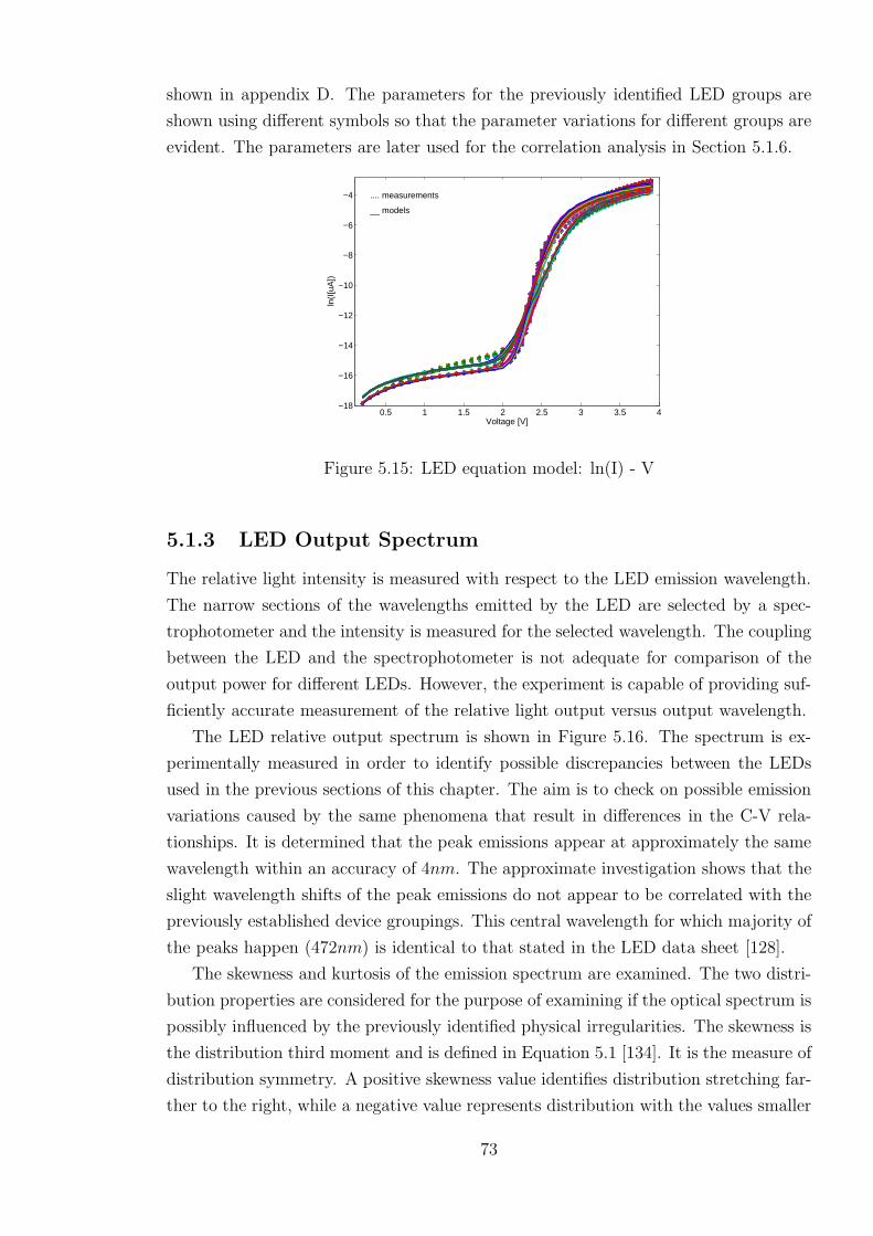
shown in appendix D. The parameters for the previously identified LED groups are
shown using different symbols so that the parameter variations for different groups are
evident. The parameters are later used for the correlation analysis in Section 5.1.6.
0.5 1 1.5 2 2.5 3 3.5 4−18
−16
−14
−12
−10
−8
−6
−4
Voltage [V]
ln(I
[uA
])
.... measurements
__ models
Figure 5.15: LED equation model: ln(I) - V
5.1.3 LED Output Spectrum
The relative light intensity is measured with respect to the LED emission wavelength.
The narrow sections of the wavelengths emitted by the LED are selected by a spec-
trophotometer and the intensity is measured for the selected wavelength. The coupling
between the LED and the spectrophotometer is not adequate for comparison of the
output power for different LEDs. However, the experiment is capable of providing suf-
ficiently accurate measurement of the relative light output versus output wavelength.
The LED relative output spectrum is shown in Figure 5.16. The spectrum is ex-
perimentally measured in order to identify possible discrepancies between the LEDs
used in the previous sections of this chapter. The aim is to check on possible emission
variations caused by the same phenomena that result in differences in the C-V rela-
tionships. It is determined that the peak emissions appear at approximately the same
wavelength within an accuracy of 4nm. The approximate investigation shows that the
slight wavelength shifts of the peak emissions do not appear to be correlated with the
previously established device groupings. This central wavelength for which majority of
the peaks happen (472nm) is identical to that stated in the LED data sheet [128].
The skewness and kurtosis of the emission spectrum are examined. The two distri-
bution properties are considered for the purpose of examining if the optical spectrum is
possibly influenced by the previously identified physical irregularities. The skewness is
the distribution third moment and is defined in Equation 5.1 [134]. It is the measure of
distribution symmetry. A positive skewness value identifies distribution stretching far-
ther to the right, while a negative value represents distribution with the values smaller
73
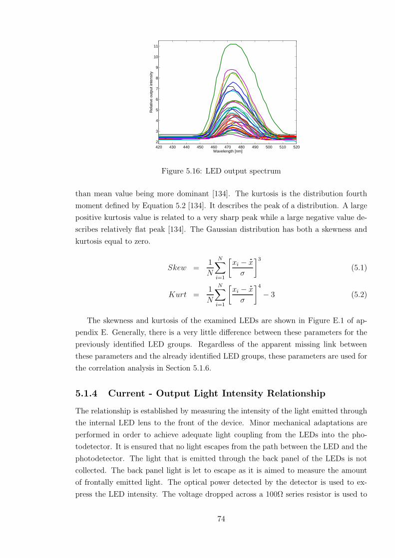
420 430 440 450 460 470 480 490 500 510 5202
3
4
5
6
7
8
9
10
11
Wavelength [nm]R
elat
ive
outp
ut in
tens
ity
Figure 5.16: LED output spectrum
than mean value being more dominant [134]. The kurtosis is the distribution fourth
moment defined by Equation 5.2 [134]. It describes the peak of a distribution. A large
positive kurtosis value is related to a very sharp peak while a large negative value de-
scribes relatively flat peak [134]. The Gaussian distribution has both a skewness and
kurtosis equal to zero.
Skew =1
N
N∑
i=1
[
xi − x
σ
]3
(5.1)
Kurt =1
N
N∑
i=1
[
xi − x
σ
]4
− 3 (5.2)
The skewness and kurtosis of the examined LEDs are shown in Figure E.1 of ap-
pendix E. Generally, there is a very little difference between these parameters for the
previously identified LED groups. Regardless of the apparent missing link between
these parameters and the already identified LED groups, these parameters are used for
the correlation analysis in Section 5.1.6.
5.1.4 Current - Output Light Intensity Relationship
The relationship is established by measuring the intensity of the light emitted through
the internal LED lens to the front of the device. Minor mechanical adaptations are
performed in order to achieve adequate light coupling from the LEDs into the pho-
todetector. It is ensured that no light escapes from the path between the LED and the
photodetector. The light that is emitted through the back panel of the LEDs is not
collected. The back panel light is let to escape as it is aimed to measure the amount
of frontally emitted light. The optical power detected by the detector is used to ex-
press the LED intensity. The voltage dropped across a 100Ω series resistor is used to
74
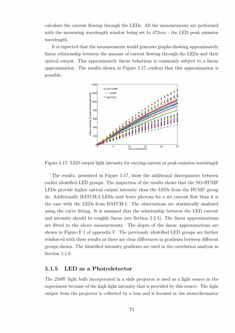
calculate the current flowing through the LEDs. All the measurements are performed
with the measuring wavelength window being set to 472nm - the LED peak emission
wavelength.
It is expected that the measurements would generate graphs showing approximately
linear relationship between the amount of current flowing through the LEDs and their
optical output. This approximately linear behaviour is commonly subject to a linear
approximation. The results shown in Figure 5.17 confirm that this approximation is
possible.
0 5 10 15 20 250
200
400
600
800
1000
1200
1400
LED Current [mA]
Out
put I
nten
sity
@ p
eak
Wav
elen
gth
[uW
]oo NO HUMP
−−−− HUMP
*** BATCH2
Figure 5.17: LED output light intensity for varying current at peak emission wavelength
The results, presented in Figure 5.17, show the additional discrepancies between
earlier identified LED groups. The inspection of the results shows that the NO-HUMP
LEDs provide higher optical output intensity than the LEDs from the HUMP group
do. Additionally BATCH-2 LEDs emit fewer photons for a set current flow than it is
the case with the LEDs from BATCH-1. The observations are statistically analysed
using the curve fitting. It is assumed that the relationship between the LED current
and intensity should be roughly linear (see Section 2.2.4). The linear approximations
are fitted to the above measurements. The slopes of the linear approximations are
shown in Figure F.1 of appendix F. The previously identified LED groups are further
reinforced with these results as there are clear differences in gradients between different
groups shown. The identified intensity gradients are used in the correlation analysis in
Section 5.1.6.
5.1.5 LED as a Photodetector
The 250W light bulb incorporated in a slide projector is used as a light source in the
experiment because of the high light intensity that is provided by this source. The light
output from the projector is collected by a lens and is focused at the monochromator
75

input. After calibration and accounting for a possible error in the form of wavelength
shift, the monochromator is controlled externally by Spectrometer Control And Data
Acquisition System software (SCADAS). This is a single beam scanning spectropho-
tometer controlled by a PC. The wavelength of the output light is scanned from 350nm
to 500nm in steps of 5nm. The light is passed through the series of filters in order to
remove unwanted higher spectral orders transmitted by the grating [135]. This output
light from the monochromator falls onto the LEDs and the potential developed across
the LED (DUT) is measured with a Digital Voltmeter (DVM). All of the components
in the experiment are aligned on an optical bench. The experiment is conducted in a
darkened environment in order to avoid interference from the external light sources with
the measurements. The system configuration is shown in Figure 5.18. The purpose
of the experiment is to compare the photogenerated LED voltage-wavelength relation-
ships. The aim is to identify possible groups of curves that might overlap with the
groups that emerged from the C-V measurements from Section 5.1.1.
Figure 5.18: LED as a photodetector - measurement setup
The measured results are shown in Figure 5.19a. The measured voltage levels vary
by a factor of four at their peak levels. It is assumed that the variations are due
to inaccurate device coupling. The variations are most certainly not related to the
previous device grouping. The curves are normalised with respect to the peak detected
voltage. The measured values are represented as a percentage of the relevant peaks.
The normalised results are shown in Figure 5.19b. The peaks for 38 of the devices
occur at 420nm (with 2.5nm accuracy). Two curves that peak at 425nm and 430nm
are detected by LED 39 and 40. These two devices exhibit significantly increased
internal capacitance. The visual curve inspection indicates that there are two distinct
groups of slopes related to the BATCH-1 devices (see Figure G.2 - appendix G). The
two groups correspond to the two groups that emerged from the C-V measurements
(i.e. HUMP and NO-HUMP).
The most concerning issue arising from the above measurements is a significant
wavelength shift for the peak emission and detection. The peaks of the emitted spectra,
which occur at 472nm, shift to 420nm when the LEDs are used as photodetectors.
This considerable and somewhat unexpected shift is assumed to be caused by the
bulk InGaN used as the active layer in the LEDs. It is reported that the blue LEDs
exhibit this wavelength shift [136]. This property can be exploited if the LEDs are
used as wavelength selective photodetectors. The photodetection spectra is reported
76

350 400 450 5000
50
100
150
200
250
300
350
400
450
Wavelength [nm]V
LE
D [m
V]
(a)
350 400 450 5000
10
20
30
40
50
60
70
80
90
100
Wavelength [nm]
V L
ED
(no
rmal
ised
)
(b)
Figure 5.19: LED used as photodetector: a) as measured, b) normalised output voltage
to coincide with the pulsing emission spectra of the devices [136].
The skewness and kurtosis of the above curves is determined in the same manner
as with the LED output spectrum in Section 5.1.3. The resulting values for these
parameters are shown in Figure G.1 in appendix G. In addition to determination of
these values, the curve fitting is also performed on the measured data. The curve fitting
is presented in appendix G.
5.1.6 Correlation
The most evident unforeseen characteristic generated by the experimental determina-
tion and analysis of the LED physical properties is the hump appearing in the LED C-V
characteristic. The inconsistent behaviour of the hump and its possible effect on LED
functioning is of a particular interest. It is also believed that the observation of such an
unwanted property could improve our understanding of the manufacturing processes
of the devices. Assuming that this property appears on regular basis, it is proposed
that the observation of this theoretically unpredicted property could potentially be
exploited for quality control purposes.
A conclusion from the analysis of the C-V characteristic (Section 5.1.1) is that this
anomaly is caused by the varying impurity concentration. It is reasonable to expect
some crystal imperfections considering that the crystallography of the materials used
for manufacture of these devices is yet to be perfected (Section 2.1). The inconsis-
tent impurity concentration causes uneven depletion layer width variation for an even
change of biasing voltage. This could potentially create anomalies as the one detected
in this case. This hypothesis (detailed in Section 5.1.1) is analysed further.
As hump causes the capacitance of the NO-HUMP LEDs to be smaller than that
of the HUMP LEDs at low forward bias it follows that the NO-HUMP LEDs should
also have wider depletion layer width. The wider depletion layer width is externally
77

observed by the need for larger biasing voltage for conduction of the same amount of
current (Figure D.1 in appendix D).
The additional argument that potentially supports the above hypothetical reasoning
for the capacitance anomaly comes from the observation of the curves generated by the
LEDs when operating as photodetectors. This mode of operation relies on the incident
photons delivering sufficient amount of energy to the electrons in the valence band so
that they are knocked out to the conduction band. The generated free electron-hole
pairs result in a current. There is a possibility that a non-uniform doping concentration
in the material alters the number of electrons in the conduction band being capable
of absorbing a photon of certain energy. Such phenomenon would alter the absorption
spectrum of the devices and hence the uneven non-Gaussian curves would be produced
as a result of the LEDs being used as photodetectors. There is a possibility that
the irregularities in the curves obtained by the LEDs when they are absorbing light
(appendix G) are caused by this non-uniform impurity concentration.
The relationships between different parameters drawn from the LED experimental
data are analysed. The parameters used for this analysis are listed in table 5.1. They
are sorted in a 40×16 matrix. The rows of the matrix represent the individual devices
and the columns are reserved for various parameters from table 5.1. The analysis is pre-
liminarily performed on all 40 devices, but is then reduced to 37 of them. The analysis
proved that the considerably atypical behaviour of the last three devices significantly
alters the correlation between the LED parameters. They are therefore excluded from
the correlation analysis and the size of the parameter matrix is therefore reduced to
37 × 16.
The matrix is first normalised so that any possible systematic error is removed from
the data. The normalised data is then analysed using singular value decomposition.
This method generates a diagonal matrix S of the same dimension as the input data
matrix and two orthogonal unitary matrices: U and V . The diagonal elements of the
matrix S are non-negative and are sorted in decreasing order. These elements are also
the singular values of the original parameter matrix. The singular values are defined
as a square root of the eigenvalues of the product between the original matrix and
its transpose. The decomposition properties are such that the following relations are
satisfied A = U ∗S ∗V T and S = UT ∗A∗V where A is the original input data matrix.
The algorithm used by MATLAB for calculation of the singular value decomposition is
defined by Anderson et al. [138]. The results of the singular value decomposition are
shown in Figure 5.20. The horizontal axis is formed by the strongest eigenvector (first
column of U matrix). The second strongest eigenvector is plotted on the vertical axis
(second column of U matrix). The plotted data shows that a result of the statistical
analysis is a distinctive LED clustering. The generated clusters coincide with the
groups of LEDs that were originally identified through the capacitance measurement,
78
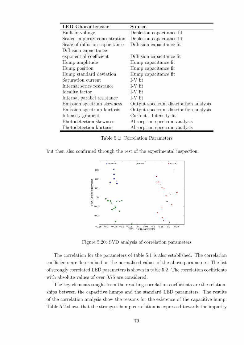
LED Characteristic SourceBuilt in voltage Depletion capacitance fitScaled impurity concentration Depletion capacitance fitScale of diffusion capacitance Diffusion capacitance fitDiffusion capacitanceexponential coefficient Diffusion capacitance fitHump amplitude Hump capacitance fitHump position Hump capacitance fitHump standard deviation Hump capacitance fitSaturation current I-V fitInternal series resistance I-V fitIdeality factor I-V fitInternal parallel resistance I-V fitEmission spectrum skewness Output spectrum distribution analysisEmission spectrum kurtosis Output spectrum distribution analysisIntensity gradient Current - Intensity fitPhotodetection skewness Absorption spectrum analysisPhotodetection kurtosis Absorption spectrum analysis
Table 5.1: Correlation Parameters
but then also confirmed through the rest of the experimental inspection.
−0.25 −0.2 −0.15 −0.1 −0.05 0 0.05 0.1 0.15 0.2 0.25
−0.2
−0.1
0
0.1
0.2
0.3
NO HUMP HUMP BATCH 2
SVD − 1st U eigenvector
SV
D −
2nd
U e
igen
vect
or
Figure 5.20: SVD analysis of correlation parameters
The correlation for the parameters of table 5.1 is also established. The correlation
coefficients are determined on the normalised values of the above parameters. The list
of strongly correlated LED parameters is shown in table 5.2. The correlation coefficients
with absolute values of over 0.75 are considered.
The key elements sought from the resulting correlation coefficients are the relation-
ships between the capacitive humps and the standard LED parameters. The results
of the correlation analysis show the reasons for the existence of the capacitive hump.
Table 5.2 shows that the strongest hump correlation is expressed towards the impurity
79
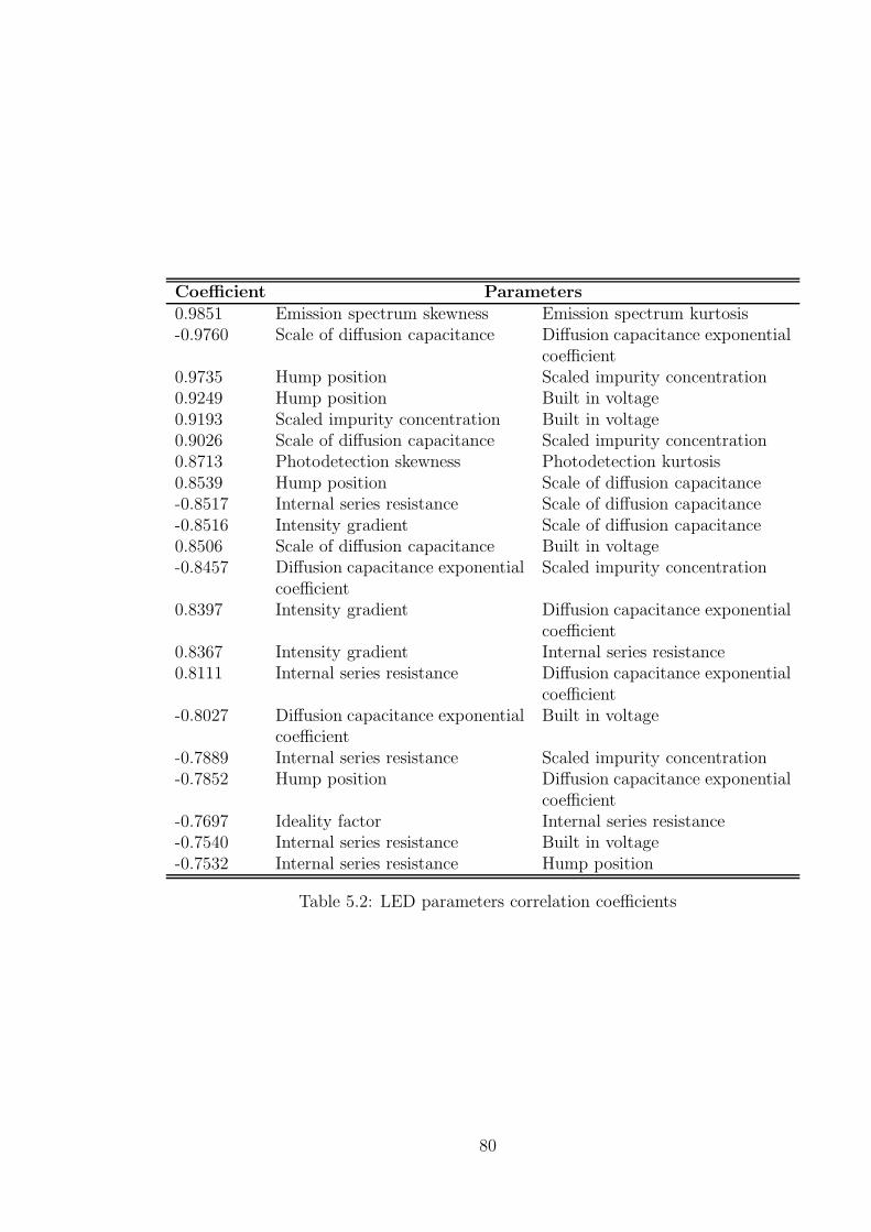
Coefficient Parameters0.9851 Emission spectrum skewness Emission spectrum kurtosis-0.9760 Scale of diffusion capacitance Diffusion capacitance exponential
coefficient0.9735 Hump position Scaled impurity concentration0.9249 Hump position Built in voltage0.9193 Scaled impurity concentration Built in voltage0.9026 Scale of diffusion capacitance Scaled impurity concentration0.8713 Photodetection skewness Photodetection kurtosis0.8539 Hump position Scale of diffusion capacitance-0.8517 Internal series resistance Scale of diffusion capacitance-0.8516 Intensity gradient Scale of diffusion capacitance0.8506 Scale of diffusion capacitance Built in voltage-0.8457 Diffusion capacitance exponential
coefficientScaled impurity concentration
0.8397 Intensity gradient Diffusion capacitance exponentialcoefficient
0.8367 Intensity gradient Internal series resistance0.8111 Internal series resistance Diffusion capacitance exponential
coefficient-0.8027 Diffusion capacitance exponential
coefficientBuilt in voltage
-0.7889 Internal series resistance Scaled impurity concentration-0.7852 Hump position Diffusion capacitance exponential
coefficient-0.7697 Ideality factor Internal series resistance-0.7540 Internal series resistance Built in voltage-0.7532 Internal series resistance Hump position
Table 5.2: LED parameters correlation coefficients
80

concentration and is followed by the relation to the built in voltage. Both of those pa-
rameters are extracted from the depletion capacitance fit. This confirms the previous
suggestion that the hump is a result of the depletion capacitance. It also supports the
assumption that the hump is directly caused by a possible abnormality in the impurity
concentration. The slightly weaker correlation of the capacitive hump position to the
LED diffusion capacitance parameters would mean that the hump is linked to either
LED current or the minority carrier lifetime (considering that the charge that causes
the diffusion capacitance is a mathematical product of the two). The minority carrier
lifetime and the diode series resistance, to which the hump is correlated in a lesser
degree, are potential results of the material impurities. This correlation analysis rein-
states the previous conclusion that the potentially non-uniform impurity concentration
has generated the capacitive humps.
5.2 Modelling Results
The theoretical basis of the models is presented in Chapter 4. The used modelling
software packages are OrCAD and MATLAB. The intention is to generate LED models
in order to help determine the requirements for the LED driving signals. The generated
models are presented in this section.
5.2.1 OrCAD Model Editor
The standard PSPICE (OrCAD) diode models are defined by the generally accepted
diode theory (Section 4.1). The selected parameters are responsible for appropriate
representation of the real device. However, optical devices are not supported. This
limitation generates the need to reuse the existing signal diode models for creation of
an adequate representation of the optical devices. This is achieved through the use of
the supplementary circuitry.
The LED model in this case is based on the use of diode current as a defining
parameter for the optical characteristics of the device. The light intensity is defined in
terms of the current flow. This is relatively simple to achieve for a steady d.c. signal.
However, the fast signal transitions proposed in this work demand the inclusion of the
device capacitance into the model. This is performed with the use of two signal diodes
connected in parallel (as shown in Figure 5.21). The two signal diodes have a very
similar set of the parameters, all of which are obtained with the use of the OrCAD
model editor. However, diode D1 is used to model electrical characteristics while diode
D2 models its optical performance.
Diode D1 allows undisturbed electrical operation of the LED driving circuit. This
is achieved by an inclusion of the capacitive parameters into this part of the model
81

Figure 5.21: LED model - using OrCAD model editor and schematic entry
so that the optical transient response of the model is realistic. These parameters do
not contribute to the light generation. The diode D2 is buffered from the rest of the
model by the use of voltage controlled voltage source E1. This allows for mathemat-
ical manipulation of the voltage dropped across the diodes with no interruption to
the driving circuit. As the cathode of the diode D2 is connected to ground through
the current controlled current source (F1) the two diodes are effectively connected in
parallel. The current that flows out of F1 is then converted to optical power. The
constant of proportionality between the current and light intensity is equal to unity for
graphical purposes. The real constant of proportionality varies for different devices and
is implemented with the use of a mathematical expression in the PSPICE netlist. The
resulting PSPICE netlist is shown in the appendix H. The parameters derived from
the model editor and used to describe the LEDs are shown as a part of the .LEDMOD
statements.
5.2.2 OrCAD Behavioural Model
The generated OrCAD behavioural model relies on Equation 4.2. A large signal real
diode model (Figure 4.2c) is implemented. It relies on current-voltage, capacitance-
voltage and current-light intensity characteristics. This approach allows observation
of the effects that each specific LED parameter has on the performance of the device
as a whole. The prospective use of the model in PSPICE environment potentially
enables assessment of the electronic driver behaviour with specific changes in the LED
characteristics.
The experimental curve fitting is performed. As the current equation is simplified,
it was found that the saturation current is dependant on the voltage applied to the
device. This is anticipated as the diode parallel resistance is ignored in the diode
equation used in this case. The junction capacitance is fitted as in Equation 5.3 (xa
is a scaling factor), which corresponds to the theoretical Equation 2.36. The diffusion
capacitance is expected to be exponential and is modelled as in Equation 5.4, where
82

xb and xc are scaling factors. The resulting diode internal capacitance is modelled as
a current source. The value of the current, sourced by the capacitor, is derived as in
Equation 5.5 where C(V ) is the intrinsic capacitance and is a sum of the junction and
diffusion capacitances. The current-intensity relationship is approximated to be linear.
Cj = xa
√
1
vbi − V(5.3)
Cd = xb exp(xcV ) (5.4)
IC = C(V )dV
dt(5.5)
The parameters obtained from the fitting procedure are employed in the LED model
shown in Figure 5.22. These parameters are related to a specific device and would
change for a different type of LED. However, the model itself should generally be
applicable to devices of the same structure.
Figure 5.22: LED behavioural PSPICE model
The current flowing from the diode’s current source is modelled mathematically
with the use of the three blocks in the top left corner of the model. The voltage drop
across the internal diode dynamic resistance is subtracted from the device voltage.
The resultant is used as an input for the calculation of the capacitive current. The
capacitance is represented in the form of current source (Equation 5.5). The junction
and diffusion capacitances are modelled by the blocks E1 and E2 respectively. The
outputs from those two blocks are true capacitances. The two are added by the block
E4, whose output represents the total device capacitance. This is multiplied by dv/dt,
inside block E5, in order to represent the capacitance as a current source. This current
is added to the modelled diode current and the resultant current flows out of the device
through the cathode. The same capacitive current is also subtracted from the diode’s
current source current and manipulated further (E3) in order to obtain optical power
83
at ’Optical Power’ port.
The main limitation of the model results from incomplete modelling of the diode
equation. This would have been acceptable had the modelled device been a p-n ho-
mojunction. However, the issues brought in with the use of heterostructure limit the
usability of the model. This is specifically noticeable in terms of parallel diode resis-
tance. The additional shortcoming of the model is that the capacitive hump is not
modelled. The reason for exclusion of this feature is that the original intent was to
model a device that would be used for circuit optimisation and the hump was considered
as an accidental feature that could be ignored.
5.2.3 MATLAB Behavioural Model
The model orientated towards the numerical analysis is based on the model of Figure
4.3 and is constructed in MATLAB (Simulink). The advantage brought in by this
model is its increased computational power and improved accuracy. This is particularly
evident in the diode equation where Lambert-W function (defined in [137]) is used in
order to improve the modelling parameters and provide more realistic representation
of the device. Consequently the parasitic resistances, which play a significant role in
the blue LEDs, are accounted for. The basis of the model is very similar to the one
of the PSPICE behavioural models. However, the emphasis in this case is put on the
particular physical parameters so that their influence on the device performance can
be observed in isolated situations. The top layer of the model is shown in Figure 5.23.
Figure 5.24 presents a lower modelling layer which is responsible for the evaluation of
the LED steady level d.c. behaviour. The other low layer, shown in Figure 5.25, is
used to determine the capacitance and the capacitive current generated by the device
when experiencing fast changing driving signals. The capacitive behaviour is derived
in the same manner as for the PSPICE behavioural model. That is, Equations 5.3,
5.4 and 5.5 are reused in order to determine the two capacitances and the capacitive
current respectively. If the hump behaviour is detected in the LED capacitance –
voltage characteristic, then the model section shown in Figure 5.26 is added to the
layer shown in Figure 5.25. The hump capacitance is in that case added to the other
two LED capacitances.
5.2.4 Model Comparison
The modelling in this case was used as an auxiliary tool that carried the potential
of enhancing the optimisation of the electronic circuit design. As it was intended
to be used as a helping tool the modelling experienced few unexpected turns. The
resulting models were not utilised to the originally planned extent, but have proved
to be valuable in terms of understanding of the LED performance. The differences
84

Figure 5.23: LED behavioural MATLAB model - top level
between the resulting three models are a product of this need for study of the specified
device and its performance.
The OrCAD (editor) model is a product of the software package, which does not
support the optical devices. The additions to the existing signal diode models allow
certain amount of integration of the optical devices with this admirable circuit design
orientated package. The result is a model that is of adequate quality for standard
applications where the LEDs are not driven by fast switching signals. However, the
use of the model editor reduces the user controllability. This is because the model editor
uses the standard theory to predict the behaviour of the device (as described in Section
4.1). Consequently the model is a crude representation of the real device if it is to be
driven by the fast altering signals. This limitation of the model was improved by the
OrCAD behavioural model, which allows greater control of the specific characteristics
of the modelled devices. At the same time, the usability in the circuit simulation
environment is maintained. Consequently, this model is a more realistic representation
of the LEDs in question. However, the mathematical limitations of the software package
prevent the accurate modelling of the LED current equation. This should not be the
case had the standard p-n homojunction device been used. The problem is possible to
resolve in OrCAD, but it was considered at the time that the benefits to the project
would be more significant if MATLAB was employed. Consequently, the final model
is the most accurate of the three in terms of diode equation and the diode internal
85
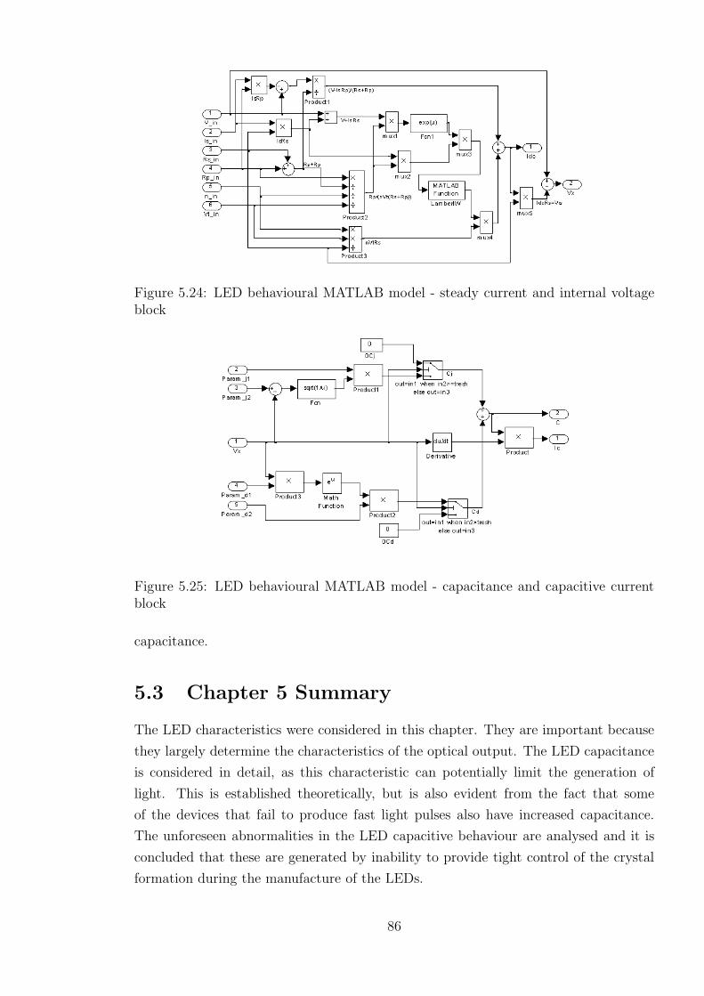
Figure 5.24: LED behavioural MATLAB model - steady current and internal voltageblock
Figure 5.25: LED behavioural MATLAB model - capacitance and capacitive currentblock
capacitance.
5.3 Chapter 5 Summary
The LED characteristics were considered in this chapter. They are important because
they largely determine the characteristics of the optical output. The LED capacitance
is considered in detail, as this characteristic can potentially limit the generation of
light. This is established theoretically, but is also evident from the fact that some
of the devices that fail to produce fast light pulses also have increased capacitance.
The unforeseen abnormalities in the LED capacitive behaviour are analysed and it is
concluded that these are generated by inability to provide tight control of the crystal
formation during the manufacture of the LEDs.
86
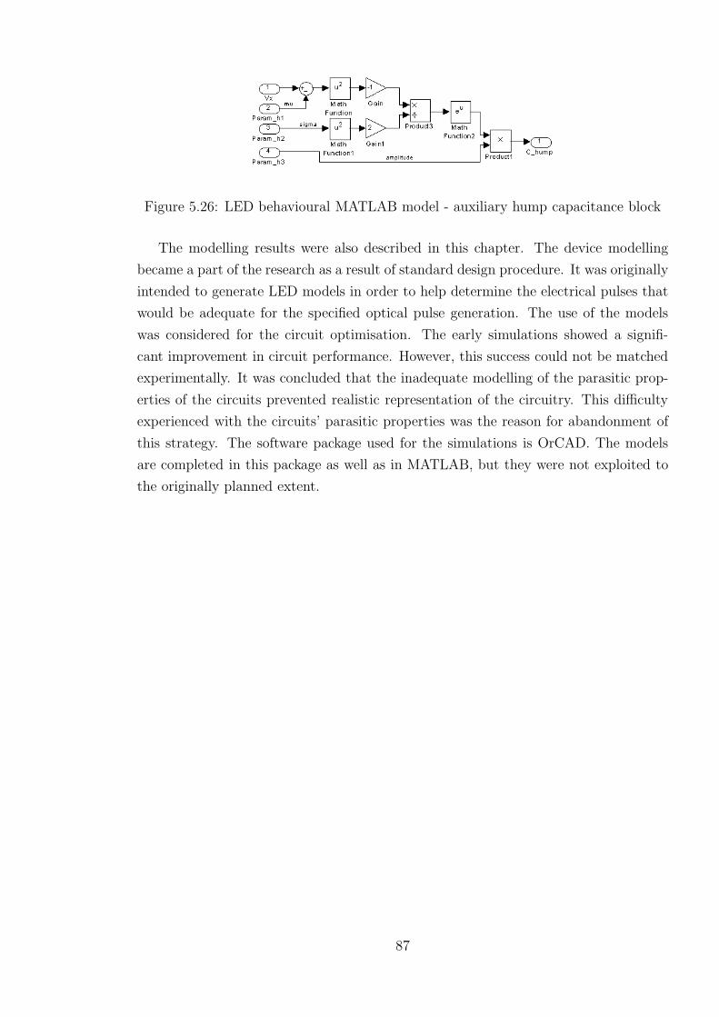
Figure 5.26: LED behavioural MATLAB model - auxiliary hump capacitance block
The modelling results were also described in this chapter. The device modelling
became a part of the research as a result of standard design procedure. It was originally
intended to generate LED models in order to help determine the electrical pulses that
would be adequate for the specified optical pulse generation. The use of the models
was considered for the circuit optimisation. The early simulations showed a signifi-
cant improvement in circuit performance. However, this success could not be matched
experimentally. It was concluded that the inadequate modelling of the parasitic prop-
erties of the circuits prevented realistic representation of the circuitry. This difficulty
experienced with the circuits’ parasitic properties was the reason for abandonment of
this strategy. The software package used for the simulations is OrCAD. The models
are completed in this package as well as in MATLAB, but they were not exploited to
the originally planned extent.
87
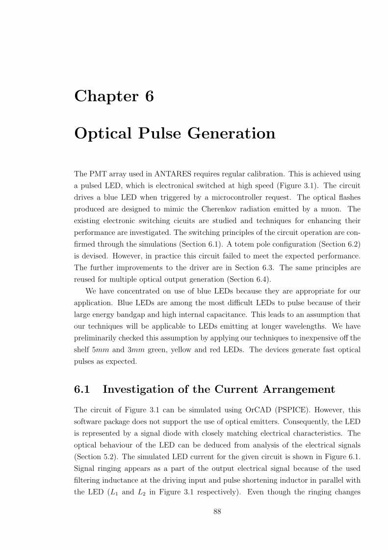
Chapter 6
Optical Pulse Generation
The PMT array used in ANTARES requires regular calibration. This is achieved using
a pulsed LED, which is electronical switched at high speed (Figure 3.1). The circuit
drives a blue LED when triggered by a microcontroller request. The optical flashes
produced are designed to mimic the Cherenkov radiation emitted by a muon. The
existing electronic switching cicuits are studied and techniques for enhancing their
performance are investigated. The switching principles of the circuit operation are con-
firmed through the simulations (Section 6.1). A totem pole configuration (Section 6.2)
is devised. However, in practice this circuit failed to meet the expected performance.
The further improvements to the driver are in Section 6.3. The same principles are
reused for multiple optical output generation (Section 6.4).
We have concentrated on use of blue LEDs because they are appropriate for our
application. Blue LEDs are among the most difficult LEDs to pulse because of their
large energy bandgap and high internal capacitance. This leads to an assumption that
our techniques will be applicable to LEDs emitting at longer wavelengths. We have
preliminarily checked this assumption by applying our techniques to inexpensive off the
shelf 5mm and 3mm green, yellow and red LEDs. The devices generate fast optical
pulses as expected.
6.1 Investigation of the Current Arrangement
The circuit of Figure 3.1 can be simulated using OrCAD (PSPICE). However, this
software package does not support the use of optical emitters. Consequently, the LED
is represented by a signal diode with closely matching electrical characteristics. The
optical behaviour of the LED can be deduced from analysis of the electrical signals
(Section 5.2). The simulated LED current for the given circuit is shown in Figure 6.1.
Signal ringing appears as a part of the output electrical signal because of the used
filtering inductance at the driving input and pulse shortening inductor in parallel with
the LED (L1 and L2 in Figure 3.1 respectively). Even though the ringing changes
88

the diode bias from reverse into forward and vice-versa, the magnitude of the swing is
heavily damped and as such does not cause the LED to emit.
Figure 6.1: Simulated output electrical pulse
Figure 6.2: Simulated transistor waveforms: top - PNP emitter-base voltage, middle -NPN base-emitter voltage, bottom - LED current
The controlling voltages for the complementary transistors at the time when LED
conducts current are shown in Figure 6.2. The signal on the top is VEB of the PNP
transistor (Q1) from Figure 3.1, while the signal in the middle of the Figure is VBE of
the NPN transistor (Q2) from the same Figure. The graph shows that the transistors
are simultaneously in either on or off state. The switching action from Figure 6.2 is
described in Section 3.4. At the conclusion of the switching action both transistors
return to the stable off state. This rapid and efficient switching forms the basis for
high speed pulse generation.
Development of this simple regenerative switch and the application of established
pulse shaping techniques are considered for creation of electrical signals suitable for the
LEDs. Further optimisation is aimed at generating required optical signal (approxi-
mately 1ns rise time and 3ns FWHM – Chapter 1). An essential feature sought from
the electrical pulse is its rise time. For reasons explained in Section 3.3 it is believed
that the rise time of the optical pulse closely follows the rise time of the electrical drive
pulse. This rise time is limited by the switching characteristics of the active devices
89
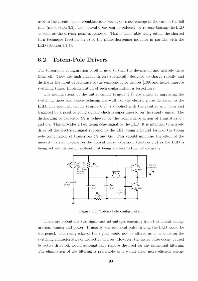
used in the circuit. This resemblance, however, does not emerge in the case of the fall
time (see Section 3.3). The optical decay can be reduced by reverse biasing the LED
as soon as the driving pulse is removed. This is achievable using either the shorted
turn technique (Section 3.2.6) or the pulse shortening inductor in parallel with the
LED (Section 3.1.4).
6.2 Totem-Pole Drivers
The totem-pole configuration is often used to turn the devices on and actively drive
them off. They are high current drivers specifically designed to charge rapidly and
discharge the input capacitance of the semiconductor devices [139] and hence improve
switching times. Implementation of such configuration is tested here.
The modifications of the initial circuit (Figure 3.1) are aimed at improving the
switching times and hence reducing the width of the electric pulse delivered to the
LED. The modified circuit (Figure 6.3) is supplied with the positive d.c. bias and
triggered by a positive going signal, which is superimposed on the supply signal. The
discharging of capacitor C2 is achieved by the regenerative action of transistors Q1
and Q2. This provides a fast rising edge signal to the LED. It is intended to actively
drive off the electrical signal supplied to the LED using a hybrid form of the totem
pole combination of transistors Q2 and Q3. This should minimise the effect of the
minority carrier lifetime on the optical decay expansion (Section 3.3) as the LED is
being actively driven off instead of it being allowed to turn off naturally.
Figure 6.3: Totem-Pole configuration
There are potentially two significant advantages emerging from this circuit config-
uration: timing and power. Primarily, the electrical pulse driving the LED would be
sharpened. The rising edge of the signal would not be altered as it depends on the
switching characteristics of the active devices. However, the faster pulse decay, caused
by active drive off, would automatically remove the need for any sequential filtering.
The elimination of the filtering is preferable as it would allow more efficient energy
90
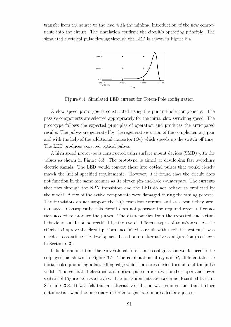
transfer from the source to the load with the minimal introduction of the new compo-
nents into the circuit. The simulation confirms the circuit’s operating principle. The
simulated electrical pulse flowing through the LED is shown in Figure 6.4.
Figure 6.4: Simulated LED current for Totem-Pole configuration
A slow speed prototype is constructed using the pin-and-hole components. The
passive components are selected appropriately for the initial slow switching speed. The
prototype follows the expected principles of operation and produces the anticipated
results. The pulses are generated by the regenerative action of the complementary pair
and with the help of the additional transistor (Q3) which speeds up the switch off time.
The LED produces expected optical pulses.
A high speed prototype is constructed using surface mount devices (SMD) with the
values as shown in Figure 6.3. The prototype is aimed at developing fast switching
electric signals. The LED would convert these into optical pulses that would closely
match the initial specified requirements. However, it is found that the circuit does
not function in the same manner as its slower pin-and-hole counterpart. The currents
that flow through the NPN transistors and the LED do not behave as predicted by
the model. A few of the active components were damaged during the testing process.
The transistors do not support the high transient currents and as a result they were
damaged. Consequently, this circuit does not generate the required regenerative ac-
tion needed to produce the pulses. The discrepancies from the expected and actual
behaviour could not be rectified by the use of different types of transistors. As the
efforts to improve the circuit performance failed to result with a reliable system, it was
decided to continue the development based on an alternative configuration (as shown
in Section 6.3).
It is determined that the conventional totem-pole configuration would need to be
employed, as shown in Figure 6.5. The combination of C3 and R4 differentiate the
initial pulse producing a fast falling edge which improves device turn off and the pulse
width. The generated electrical and optical pulses are shown in the upper and lower
section of Figure 6.6 respectively. The measurements are taken as described later in
Section 6.3.3. It was felt that an alternative solution was required and that further
optimisation would be necessary in order to generate more adequate pulses.
91

Figure 6.5: Full Totem-Pole configuration
−1
0
1
2
3
4
5
6
Driv
ing
Vol
tage
[V]
0 2 4 6 8 10 12 14 16 18 20
−0.5
−0.4
−0.3
−0.2
−0.1
0
0.1
time [ns]
PM
T o
utpu
t [V
]
Figure 6.6: Experimantally obtained totem-pole output signal
6.3 Single Output Configurations
The single output drivers are configured so there is a single LED used per driver.
Consequently, the output is a single optical signal. These, originally intended, drivers
are of the main interest. However, the possibility of using a multiple output drivers
and their potential for the reduction of size, complexity and cost is rationally exploited
resulting in development of multiple output drivers (Section 6.4).
6.3.1 Switching Configuration
The previously considered cross coupled pair of complementary transistors is reused.
The redeveloped free running oscillatory circuit is shown in Figure 6.7. The specified
component values are designed to produce pulses with a rise time of 2.9ns at a repetition
frequency of approximately 23kHz. The component values (especially C1) are chosen
to optimise speed of the pulses. The repetition rate is arbitrary and is determined by
R1, R2, R3 and C1.
Initially C1 is uncharged and hence has zero voltage across it. Transistors Q1 and
92

Figure 6.7: New driver standard configuration
Q2 are both in the off state. The potential Vref is then defined by the potential divider
formed by R2 and R3. Capacitor C1 charges through R1. When the voltage across this
capacitor exceeds Vref by the amount of base-emitter voltage of transistor Q1 the same
transistor starts to conduct. This turns on Q2 which causes Vref to fall quickly turning
Q1 fully on. This action provides a low impedance path for capacitor C1 to discharge
through R4 and C3 causing the regenerative switch to return to its initial condition.
The values of C3 and R4 have been established empirically to give optimum results
when driving an Agilent blue LED of type HLMP-CB15 [128] and the pulse forming
network attached to the circuit board between points X and Y . The free running
period is controlled by the time constant R1C1 and the magnitude of Vref . The rise
time of the output pulse developed across R4 is a function of the switching speeds of
Q1 and Q2 while the turn off time is dictated by the discharge current path formed by
Q1, Q2, R4 and the value of C1. Capacitor C2 provides a small amount of feedback
which enhances the initial ‘turn on’ time of the pulse.
By varying the supply voltage, VCC , a family of output curves (measured across
R4) can be produced as shown in Figure 6.8 where the curves A to E correspond to
different supply voltages. The ringing on the graph is assumed to be caused by parasitic
impedance and non-uniform impedance mismatch of the probe cable.
By removing R3 and connecting a capacitor Ct to point Vref the device can be
externally triggered by a negative pulse. The points X and Y in Figure 6.7 are the
positions where the LED and its associated pulse forming network is connected.
6.3.2 Pulse Shaping
Figures 6.9 illustrate the four pulse shaping circuits considered. In each case, the
points X and Y correspond to those in Figure 6.7. Diode pulse shaping is achieved
93
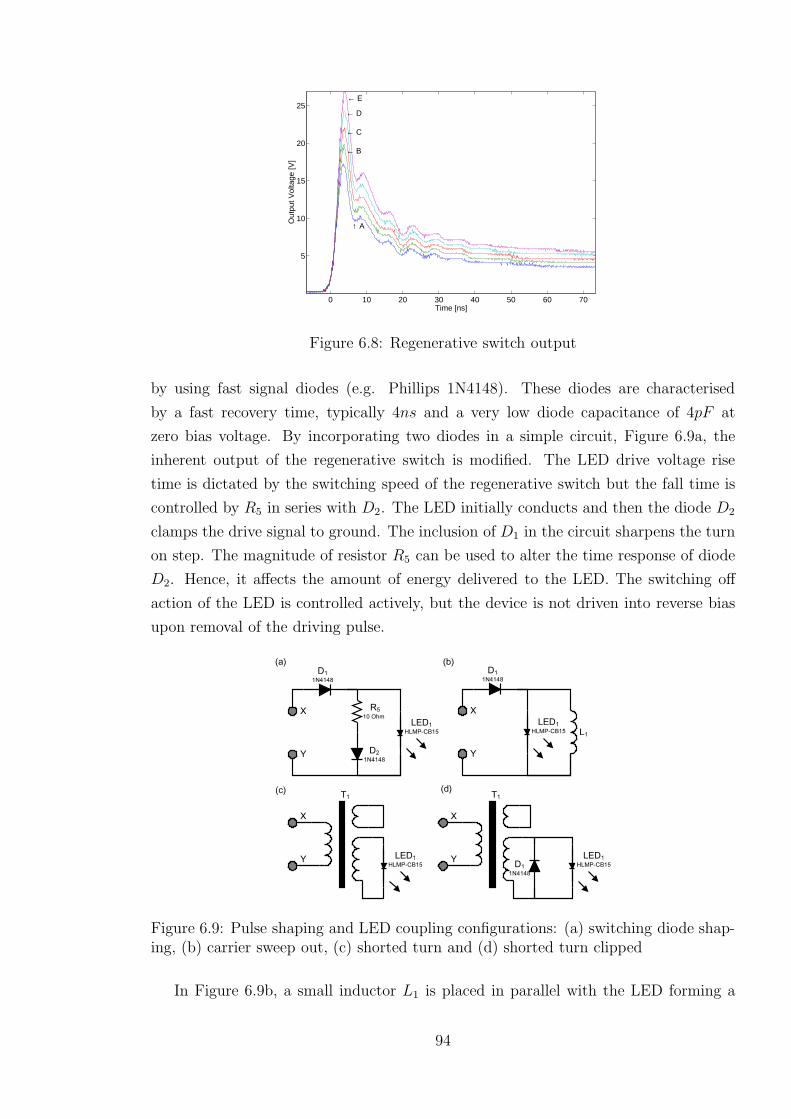
0 10 20 30 40 50 60 70
5
10
15
20
25
Time [ns]
Out
put V
olta
ge [V
]
↑ A
← B
← C
← D
← E
Figure 6.8: Regenerative switch output
by using fast signal diodes (e.g. Phillips 1N4148). These diodes are characterised
by a fast recovery time, typically 4ns and a very low diode capacitance of 4pF at
zero bias voltage. By incorporating two diodes in a simple circuit, Figure 6.9a, the
inherent output of the regenerative switch is modified. The LED drive voltage rise
time is dictated by the switching speed of the regenerative switch but the fall time is
controlled by R5 in series with D2. The LED initially conducts and then the diode D2
clamps the drive signal to ground. The inclusion of D1 in the circuit sharpens the turn
on step. The magnitude of resistor R5 can be used to alter the time response of diode
D2. Hence, it affects the amount of energy delivered to the LED. The switching off
action of the LED is controlled actively, but the device is not driven into reverse bias
upon removal of the driving pulse.
Figure 6.9: Pulse shaping and LED coupling configurations: (a) switching diode shap-ing, (b) carrier sweep out, (c) shorted turn and (d) shorted turn clipped
In Figure 6.9b, a small inductor L1 is placed in parallel with the LED forming a
94

resonant circuit. This allows the voltage across the LED to swing negative. Its shape
is controlled by the amplitude of the initial pulse and the voltage dependence of the
depletion capacitance of the LED. In general terms it is a damped oscillator. L1 is
constructed from six turns of 0.54mm diameter enamel covered copper wire wound on
a 5mm diameter former. The coil is self-supporting on the circuit board. It has value
of 0.19µH measured at 100kHz.
The transformer in the circuit Figure 6.9c is fabricated by a bifilar winding of
three turns of 0.54mm enamel coated copper wire on a toroidal former (Ferroxcube,
type TN9/6/3-4C65). An additional two turns of the same type of wire are placed
centrally and directly on top of these windings. These additional turns are shorted
together. This configuration forms a pulse transformer whose self-inductance is 0.50µH
measured at 100kHz. A pulse transformer with shorted turns effectively differentiates
the input drive pulse. This is caused by the prompt collapse of the magnetic flux
within the ferrite core due to the influence of the shorted turns which act as a very low
impedance secondary winding. The result of this action is a rapid negative swing. At
the operational frequency of the circuit, the physical properties of the ferrite core are
at the upper limits of their specification. On the negative swing of the drive voltage the
waveform is a function of the inductance of the transformer and the LED capacitance.
Modifying this circuit by the inclusion of a clamping diode D1, Figure 6.9d, restricts
the negative swing and subsequent overshoot.
6.3.3 Measurement Technique
The photomultiplier tube (Hamamatsu R7400U) and its associated circuitry are housed
in a small metal box (Hamamatsu H6780 PMT module). Typical rise time and electron
transit times for the PMT are 0.78ns and 5.4ns respectively. A coupling assembly
is used to interface light sources to the optical window of the photomultiplier tube.
The LED is held 4mm from the optical window. The gain of the PMT is controlled
by a potentiometer which allows the output voltage of the PMT to be adjusted and
maintained at a constant level for a wide range of optical intensities. Figure 6.10 is a
schematic showing the equipment layout used for evaluation of the drive and optical
pulses. The oscilloscope bandwidth is 500MHz with the sampling rate of 2 Giga-
Samples per second. The type of the probes used in the experiment is Tek P6137 and
their capacitance is 10.8 pF . Data were collected and stored in a spreadsheet using
Agilent IntuiLink 54600 software. The data is taken from a still measurement. The
captured screen data is sampled at 1000 samples per screen shot. This increases the
apparent sampling rate. The jitter obtained from the graphs in the following section
are the result of this apparent sampling rate which gives the feel of the signals being
sampled at the rate faster than actual. MATLAB is used for data plotting.
95

Figure 6.10: Measurements - experimental configuration
6.3.4 Results and Discussion
The narrowest pulses achieved experimentally without pulse shaping have 5ns FWHM.
The minimum voltage required to stimulate light production using such driving pulses
is 5.2V . When the oscilloscope probe was connected to the circuit, this condition was
satisfied for a VCC of 15V . The amplitude of all of the LED drive pulses are controlled
by varying the magnitude of VCC in three steps of 2V from the point when the circuit
starts generating an optically significant signal. This corresponds to a drive voltage
of 12V for circuit in Figure 6.9a, 13V for the circuit in Figure 6.9b and 17V for the
circuits in Figures 6.9c and 6.9d. Figures 6.11-6.14 show the measured input drive
signal and the observed optical signal for the four circuits illustrated in Figures 6.9a-d.
In each Figure the curves A – D correspond to first optically significant signal (A),
+2V (B), +4V (C), +6V (D).
From Figure 6.11, it can be seen that a simple diode pulse shaping technique can
produce a well defined LED driving pulse. By altering VCC over the stated range of
voltages, the current flowing through the LED is altered accordingly. Curve A at the
bottom of Figure 6.11 shows a well defined optical pulse which closely mirrors the drive
pulse. The delay between the two pulses is caused by the time taken to produce the
optical pulse and the electron transit time of the PMT. As the drive voltage is increased
there is a corresponding increase in the decay time of the optical pulse B, C and D.
Higher drive voltages inject more carriers into the LED. The recombination time taken
for these to be neutralised by a fixed number of photon producing traps within the
fabric of the LED is also increased. Hence longer decay times are seen in the optical
pulse.
In Figure 6.12 it can be clearly seen that swinging the drive voltage negative sig-
nificantly reduces the decay time of the optical pulse. In effect, this technique removes
the excess carriers from the LED’s active region. This is analogous to discharging the
diffusion capacitance of the LED. The negative portion of the drive pulse is slow to
reach its maximum voltage and has an extended duration of 2.5 times that of the drive
pulse. This shape is not optimal for the efficient removal of the excess carriers.
96
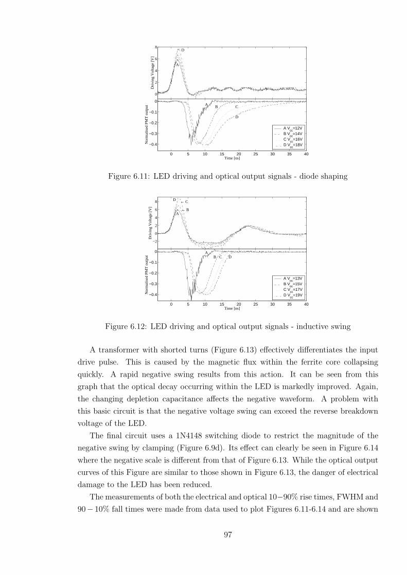
0
2
4
6
8
Driv
ing
Vol
tage
[V]
A
D
0 5 10 15 20 25 30 35 40
−0.4
−0.3
−0.2
−0.1
0
Time [ns]
Nor
mal
ised
PM
T o
utpu
t
A B C
D
A Vcc
=12VB V
cc=14V
C Vcc
=16VD V
cc=18V
Figure 6.11: LED driving and optical output signals - diode shaping
−2
0
2
4
6
8
Driv
ing
Vol
tage
[V]
A← B
← CD
0 5 10 15 20 25 30 35 40
−0.4
−0.3
−0.2
−0.1
0
Time [ns]
Nor
mal
ised
PM
T o
utpu
t AB C D
A Vcc
=13VB V
cc=15V
C Vcc
=17VD V
cc=19V
Figure 6.12: LED driving and optical output signals - inductive swing
A transformer with shorted turns (Figure 6.13) effectively differentiates the input
drive pulse. This is caused by the magnetic flux within the ferrite core collapsing
quickly. A rapid negative swing results from this action. It can be seen from this
graph that the optical decay occurring within the LED is markedly improved. Again,
the changing depletion capacitance affects the negative waveform. A problem with
this basic circuit is that the negative voltage swing can exceed the reverse breakdown
voltage of the LED.
The final circuit uses a 1N4148 switching diode to restrict the magnitude of the
negative swing by clamping (Figure 6.9d). Its effect can clearly be seen in Figure 6.14
where the negative scale is different from that of Figure 6.13. While the optical output
curves of this Figure are similar to those shown in Figure 6.13, the danger of electrical
damage to the LED has been reduced.
The measurements of both the electrical and optical 10−90% rise times, FWHM and
90− 10% fall times were made from data used to plot Figures 6.11-6.14 and are shown
97

−6
−4
−2
0
2
4
6
Driv
ing
Vol
tage
[V] A
D
0 5 10 15 20 25 30 35 40
−0.4
−0.3
−0.2
−0.1
0
Time [ns]
Nor
mal
ised
PM
T o
utpu
t
AB ← C
DA V
cc=17V
B Vcc
=19VC V
cc=21V
D Vcc
=23V
Figure 6.13: LED driving and optical output signals - shorted turn
−4
−2
0
2
4
6
Driv
ing
Vol
tage
[V] A
D
0 5 10 15 20 25 30 35 40
−0.4
−0.3
−0.2
−0.1
0
Time [ns]
Nor
mal
ised
PM
T o
utpu
t
AB ← C
DA V
cc=17V
B Vcc
=19VC V
cc=21V
D Vcc
=23V
Figure 6.14: LED driving and optical output signals - clipped shorted turn
in table 6.1. Only the best (plot A) and worst (plot D) parameters have been tabulated
for the various pulse forming circuits, Figure 6.9. It can be observed that in all cases
the positive component of the drive voltage have similar timing characteristics. In the
simple circuit (Figure 6.9a) it can be readily seen that for a low LED drive voltage
(hence current) the optical pulse closely follows the stimulating voltage. The delay
between the drive voltage and the optical pulse is the time taken for the blue LED to
produce its optical signal and be detected by the PMT. The light generation is dictated
by the structure of the device and the quantum processes involved. At higher drive
voltages (larger currents) the time for the excess carriers to recombine with the fixed
number of traps within the semiconductor junction extends the optical decay time.
By allowing the drive voltage to swing negative (Figure 6.12) the excess carriers can,
to some extent, be removed from the active region thus speeding up the optical pulse.
The simple inductive circuit used to achieve this, Figure 6.12, has a slow negative time
response and as such is inefficient in carrying out this task. Circuits (Figure 6.13 and
98
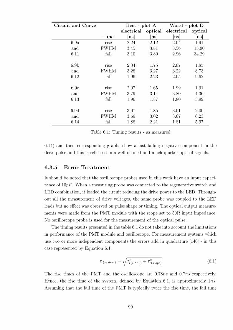
Circuit and Curve Best - plot A Worst - plot Delectrical optical electrical optical
time [ns] [ns] [ns] [ns]6.9a rise 2.24 2.12 2.04 1.91and FWHM 3.45 3.81 3.56 13.906.11 fall 3.10 3.80 2.96 34.29
6.9b rise 2.04 1.75 2.07 1.85and FWHM 3.28 3.27 3.22 8.736.12 fall 1.96 2.23 2.05 9.62
6.9c rise 2.07 1.65 1.99 1.91and FWHM 3.79 3.14 3.80 4.366.13 fall 1.96 1.87 1.80 3.99
6.9d rise 3.07 1.85 3.01 2.00and FWHM 3.69 3.02 3.67 6.236.14 fall 1.88 2.21 1.81 5.97
Table 6.1: Timing results - as measured
6.14) and their corresponding graphs show a fast falling negative component in the
drive pulse and this is reflected in a well defined and much quicker optical signals.
6.3.5 Error Treatment
It should be noted that the oscilloscope probes used in this work have an input capaci-
tance of 10pF . When a measuring probe was connected to the regenerative switch and
LED combination, it loaded the circuit reducing the drive power to the LED. Through-
out all the measurement of drive voltages, the same probe was coupled to the LED
leads but no effect was observed on pulse shape or timing. The optical output measure-
ments were made from the PMT module with the scope set to 50Ω input impedance.
No oscilloscope probe is used for the measurement of the optical pulse.
The timing results presented in the table 6.1 do not take into account the limitations
in performance of the PMT module and oscilloscope. For measurement systems which
use two or more independent components the errors add in quadrature [140] - in this
case represented by Equation 6.1.
τr(system) =√
τ 2r(PMT ) + τ 2
r(scope) (6.1)
The rise times of the PMT and the oscilloscope are 0.78ns and 0.7ns respectively.
Hence, the rise time of the system, defined by Equation 6.1, is approximately 1ns.
Assuming that the fall time of the PMT is typically twice the rise time, the fall time
99

of the system, defined by Equation 6.2, approximates to 1.7ns.
τf(system) =√
τ 2f(PMT ) + τ 2
f(scope) (6.2)
A general approximation of the FWHM being equal to the sum of the rise and fall
times of the system yields approximate value for the system FWHM of 2.7ns. This is
the response of the system to a delta function light flash. This response degrades the
observed FWHM according to Equation 6.3 which can thus be used to calculate the
optical FWHM.
FWHM(optical) =√
FWHM2(observed) − FWHM2
(system) (6.3)
The calculated timing characteristics of the best-achieved optical signals are listed in
table 6.2.
Circuit and Curve trise [ns] FWHM [ns] tfall [ns]6.9a and 6.11 (A) 1.04 2.73 4.236.9b and 6.12 (A) 1.04 2.20 2.766.9c and 6.13 (A) 0.73 1.31 2.226.9d and 6.14 (A) 0.80 0.74 2.10
Table 6.2: Best achieved timing results
The measurements are repeated using a LeCroy (waveRunner 6100 1GHz) oscil-
loscope with the typical rise time of 0.4ns. The calculated timing characteristics of
optical signals from the repeated measurements are in agreement within experimental
error with the results shown in table 6.2.
A possible alternative method for evaluating the timing characteristic of the gener-
ated light flashes employs the single photon technique [141]. This procedure requires
two PMTs. One of those, which collects large amount of light from the flashing device,
provides a zero-time signal by sensing the formation of the first few photoelectrons
at its cathode. The other PMT is set in such a way that its probability of photon
detection per pulse is much less than one. The pulse shape is determined by construct-
ing a histogram of the time differences between two PMT signals over many flashes.
This technique is more accurate and with off the shelf components generates a FWHM
accuracy of approximately 100ps [142].
6.4 Multiple Output Configuration
Even though the single output LED drivers are of the main interest for the intended
PMT calibrating application, the possibility of developing the additional functionalities
from slightly altered driver could prove to be significant. A multiple optical output
100

circuitry offers three additional functions. Primarily, it has a potential of providing an
option for PMT intensity calibration. To achieve this function, different LEDs emit
light of different intensities. Hence, the optical intensity ought to be easily adjustable
for individual LEDs. A train of optical pulses provides an identity stamp for the
PMTs, so that any noise signals can be filtered out through the pattern recognition.
This function requires delay lines achievable through either electrical or optical pulse
delay. The ability to control the delay and the intensity could potentially be exploited
for other short-lifetime fluorescence investigating applications. The final benefit from
the multiple output drivers comes from the reduction of the device count for the same
optical output capability. The optical outputs of these drivers are relatively similar to
the outputs achieved by the single LED drivers, but the circuits are reduced in size.
Hence, there are likely benefits in terms of size, cost and power consumption.
6.4.1 Circuit Arrangement
The single optical output circuit (Figure 6.7) is reconfigured with the aim of developing
a multiple optical output driver, shown in Figure 6.15. The circuit relies on operation
of complementary pair regenerative switch. The switch consists of transistors Q1 and
Q2. This section of the circuit obeys the same principles used by the single output
driver (Section 6.3). The main addition to that circuit in terms of pulse generation
is transistor Q3. This transistor helps discharge the storage capacitor C1 when the
regenerative switch enters the on state. The outcome is reduction of decay time and
FWHM. Transistor Q3 is biased with the resistor combination R2 – R3. The additional
inductor L1 aids the switching off process. The inductor comprises of 5 turns of 0.54mm
diameter enamel covered copper wire wound on a 8mm diameter former. The resulting
inductance of the constructed inductor is 0.095µH as measured at 100kHz. The benefit
of using the inductor L1 in the circuit is evident in Figure 6.16, which shows the output
from transistor Q2 when a 33 Ω dummy load is used between emitter of the output
transistor Q4 and the ground. Two curves show the switch performance with and
without the inductor L1. Even though the rise time of the switch remains the same,
the experimentally determined fall time and the FWHM are reduced from 2.38ns to
1.54ns and from 4.36ns to 3.66ns respectively.
The introduction of transistor Q3 and its supporting components improves the
driver timing characteristics. This timing enhancement is offset by a significant re-
duction in power transfer to the regenerative switch output. Hence, the additional
transistor Q4 is added to the circuit to allow sufficient current delivery to the output
LEDs. The collector d.c. current rating for this transistor is 0.5A. The transistor gain-
bandwidth product depends on the collector current. For small currents this product
is approximately one quarter of its optimal value (800MHz). This characteristic pre-
101

Figure 6.15: Multiple optical output circuit configuration
−20 −10 0 10 20
−4
−2
0
2
4
6
8
time [ns]
Vol
tage
[V]
sw o/p no coilsw o/p coil
Figure 6.16: Switch output with 33 Ohm dummy load (with and without reg. sw. coil)
vented the use of this transistor and its complementary counterpart in regenerative
switch configuration. It is experimentally established that the timing action of the
transistors, when configured as the regenerative switch, is poorer than it is the case
with the transistors employed. On the contrary, the common emitter configuration
(Figure 6.15) provides adequate collector current flow to enable exploitation of optimal
gain-bandwidth product and hence faster switching action. The fast switching base
current supplied to transistor Q4 is generated by the regenerative switch. Transistor
Q4 is able to rapidly respond to this signal and provide adequate current for the output
LEDs.
The intensity control is provided with a series link consisting of a 33Ω resistor and
a 100Ω variable resistor. The setting of the variable resistance changes the impedance
102

of the path parallel to the LEDs and furthermore alters the amount of current flowing
through the LEDs. The intensity control outcome for a single LED is shown in Figure
6.17.
0 5 10 15 20−2
−1.8
−1.6
−1.4
−1.2
−1
−0.8
−0.6
−0.4
−0.2
0
time [ns]
PM
T o
utpu
t [V
]
Figure 6.17: Intensity control on a single LED
The multiple outputs can be used as simultaneous multidirectional sources or as
fast repeating multiple flashes pointing in the same direction. If the LED outputs are
optically coupled and one of the signals is delayed, the optical pulse train shown in
Figure 6.18a is generated. As the optical output intensity is adjustable for individual
LEDs independently of each other, various intensity and delay patterns are achievable.
One of those is shown in Figure 6.18b. The delay is realised in this case with different
lengths of coaxial cable connecting the LEDs to the emitter of transistor Q4. An
alternative, and possibly improved solution in terms of signal dispersion, could involve
optical delay through a length of optical fibre. This method produces the same train
of optical pulses.
−1
−0.8
−0.6
−0.4
−0.2
0
PM
T o
utpu
t [V
]
(a)
0 10 20 30 40 50
−1
−0.8
−0.6
−0.4
−0.2
0
time [ns]
PM
T o
utpu
t [V
]
(b)
Figure 6.18: Independent intensity control on two LEDs
103

Figure 6.19 shows the detected optical pulses with the PMT set to its highest sen-
sitivity. Hence, the signals are more disturbed by the noise. This Figure is used to
measure timing characteristics of the two pulses in order to compare possible discrep-
ancies caused by the delay line. It emerges that 18ns delay causes no significant pulse
alterations. The measured timing characteristics of the two pulses are shown in table
6.3.
0 10 20 30 40
−0.5
−0.4
−0.3
−0.2
−0.1
0
time [ns]
PM
T o
utpu
t [V
]
Figure 6.19: Low optical output timing characteristics
Pulse trise [ns] FWHM [ns] tfall [ns]leading 1.40 3.10 2.92lagging 1.42 2.92 3.10
Table 6.3: Double output pulse timing
6.5 Chapter 6 Summary
The investigation of the current experimental setup was carried out. The understanding
of this arrangement and the theoretical appreciation of the pulse generating and shaping
techniques have provided the opportunity for improvement of the LED drivers. It was
demonstrated that the newly designed pulses are can produce fast optical signals from
LEDs. Taking into account measurement errors a FWHM time of below 1 ns has
been achieved. The simplicity of the circuits allows them to be either free running or
externally triggered.
The additional functionalities were offered through the use of the multiple optical
output drivers. These could be used either as multidirectional sources of light or to
generate the train of optical pulses with individually controllable intensity.
104
Chapter 7
Conclusions and Recommendations
for Further Work
This chapter draws conclusion on the important findings achieved in this research. Rec-
ommendations are also made concerning possible further work, which may be applied
to contribute to development in this area.
7.1 Conclusions
This research has studied the possibility of using blue LEDs for generation of nanosec-
ond range optical pulses. An important part of this experimental program involved
the building and optimisation of a practical prototype that would be applicable to
the calibration of neutrino detection experiments. The findings are not limited to this
application and could be used in a wide range of areas.
A simple regenerative switch using complementary transistors is used in conjunc-
tion with simple pulse shaping circuits to produce nanosecond range electronic pulses.
These pulses are optimised for active switching of the LED current flow. We demon-
strate these pulses are able to overcome the limitations exhibited by the LED material
structure. At higher drive currents simple negative transients successfully sweep out
the excess carriers from the LED junction. This allows higher intensity blue flashes to
be generated. The fast rising optical pulses are actively driven off so that the expected
decay of the light output is significantly reduced. This is achieved with the minimal
generation of the normally occurring electronic signal ringing. This results with the
blue optical pulses whose timing characteristics are worthy of use in calibration of the
PMTs and simulation of the Cherenkov radiation in the seawater. Taking into account
measurement errors a FWHM time of below 1ns has been achieved. The simplicity of
the circuits allows them to be either free running or externally triggered for synchro-
nisation purposes. The time jitter between the electrical and optical signals when the
105
driver is externally triggered is minimal. Hence, the driver is a reliable option for the
required distance measurement in underwater astroparticle detectors.
A possibility of the multiple output generation from a single electronic driver is
investigated. These drivers can be used either as the simultaneous multidirectional
optical sources or as generators of the series of flashes pointing in the same direction.
The predefined delay between the pulses is achievable. The optical output intensity is
independently adjustable for the individual LEDs. Hence, various intensity and delay
patterns are achievable. These features expand the potential range of applications and
also extend the prospect of cost reducing in large experimental setups where many
optical sources are required for calibration.
In addition to the main experimental results we have discovered that a certain num-
ber of the tested LEDs exhibit an unexpected hump-like behaviour in their capacitance-
voltage relationship. We have provided adequate reasoning for the existence of this
phenomenon and also suggest a possible approach that could make use of this feature
in manufacturing quality control.
The work has also on the sideline resulted in an analytical solution of the full diode
equation, which takes into account the negative outcomes of the parasitic resistance.
Our solution differs from the ones that were previously reported in a sense that we
consider both parasitic resistances simultaneously. The generated solution is expressed
in the form of an explicit equation. This solution eases the process of theoretical curve
fitting to the experimental data.
7.2 Further Work
The emphasis of this study has been on the development of electronic LED driver able
to produce nanosecond range blue optical pulses. There is a potential of furthering our
development so that pulses with improved light intensity and timing characteristics
are obtained. The following recommendations suggest the possible direction that the
further work might take if the additional development is to take place in the area.
• The relationship between the current flowing through the LED and the output
light intensity is commonly approximated to be linear. Apart from the clear non-
linear regions at the very low and very high bias this approximation is relatively
accurate. However, this relationship is established at d.c. conditions and it is
not clear yet if such estimate can be applied at higher switching speeds. The
relationship ought to be investigated at higher frequencies of operation.
• The capacitance - voltage relationship of the LED in low forward bias is somewhat
difficult to model because of the unpredictable nature of the depletion capaci-
tance. This capacitive component theoretically tends to infinity at low forward
106
bias as the depletion layer width tends to zero. It then instantly falls to zero
once the depletion layer is removed. Such behaviour is impracticable, but is
also difficult to measure. Detailed model of the forward bias capacitance would
significantly improve the LED models used for high frequency simulations.
• Further improvements are required should the models generated in this thesis be
utilised to their full extent in a-priori pulse circuit design.
• Generation of behavioural LED models from material structure profiles would
resolve the issue of parasitic capacitances and inductances. Such models would
be more suitable for detailed circuit simulation.
• It is credible that sub-nanosecond pulses using LEDs are possible to achieve.
However, the light intensity of such pulses is likely to be very poor. Further
investigation in the field is required if the intensity of such short pulses is to be
improved.
• The integration of the recently developed 1W and 5W LEDs and the developed
drivers is yet to be investigated
• The irregularities observed in the LED capacitance could potentially be used
for manufacturing quality control. The observed characteristics could inform
about the quality of the deposited crystals. This information could be used
for improvements of the deposition methods. Such improvements would result
in more predictable device capacitive characteristics and would most certainly
contribute to the improvement of the LED pulsing ability.
107
Appendix A
Practical Diode Equation Analysis
The conclusions are made from the inspection of the relationship between the compo-
nents of the Equation 2.30. The equation is also mathematically analysed in order to
justify the expectations for the I-V behaviour.
A.1 Analysis by inspection
There are four general areas that ought to be considered when analysing the practical
diode equation (2.30). The voltage applied to the LED defines these sections. The
areas to consider are:
• reverse bias
As V < 0 =⇒∣
∣
∣Is
exp[(
q(V −IRs)ηkT
)]
− 1∣
∣
∣≪
∣
∣
∣
V −IRs
Rp
∣
∣
∣=⇒ I ≈ V −IRs
Rp.
At reverse bias |V | ≫ |IRs| =⇒ I ≈ VRp
.
That is, the reverse bias diode current is approximately equal to the parallel resis-
tance current.
• low forward bias
The exponential term in Equation 2.30 does not become dominant at low voltage
levels. Furthermore, 1 is subtracted from this term and the difference is multiplied by
very small value of the saturation current.
It follows that∣
∣
∣Is
exp[(
q(V −IRs)ηkT
)]
− 1∣
∣
∣≪
∣
∣
∣
V −IRs
Rp
∣
∣
∣at low forward bias. Follow-
ing the argument for the reverse bias case, it follows that the LED current is approxi-
mately equal to the parallel resistance current at low forward bias.
• large forward bias
108

At large forward bias, the exponential term becomes dominant.
∴ I ≈ Is
exp[(
q(V −IRs)ηkT
)]
− 1
Expectedly, this is the standard diode equation (2.29) with the series resistance
voltage drop (−IRs) accounted. Therefore, standard diode behaviour is expected in
this region, but it should be affected by the voltage drop across the series resistance.
As the current increases, this voltage drop should become more significant.
• region between low and large forward bias
The two terms from the Equation 2.30 are comparable in magnitude in this region.
Even though the nearly exponential behaviour expected for the large forward bias is
obeyed, it is superimposed on the linear component of the parallel resistance current.
The above sections coincide with those generated by the practical diode I-V rela-
tionship (Equation 2.30 Figure 2.6).
A.2 Mathematical Analysis
The analytical algebraic solution to the Equation 2.30 proves to be somewhat compli-
cated. It is the use of both, current and voltage, on both sides of the equation that
makes the algebraic manipulation of the equation complex. The mixture of the ex-
ponential and linear terms disallows generation of explicit expression for either diode
current or voltage equation through the use of standard algebraic manipulations. It is
the use of the Lambert W function that helps resolve the issue. The function is defined
in Equation A.1.
LambertW (x) eLambertW(x) = x (A.1)
The Lambert W function has a series expansion defined by equation, but is limited
to the complex numbers whose real part is less than unity A.2 [143].
LambertW (x) =
∞∑
n=1
(−1)n−1nn−2
(n − 1)!xn (A.2)
The Symbolic Math Toolbox of the MATLAB software package is used to solve the
Equation 2.30 in terms of diode current. The solution is further simplified using the
toolbox. The solution in terms of diode current is shown in Equation A.3. The equation
109

assumes the thermal voltage to be constant throughout the measurements (Vt = kTq
).
I =1
Rs (Rs + Rp)
RsV + ηVtRpLambertW
IsRsRp exp(
Rp(V +IsRs)ηVt(Rs+Rp)
)
ηVt (Rs + Rp)
+ ηVtRsLambertW
IsRsRp exp(
Rp(V +IsRs)ηVt(Rs+Rp)
)
ηVt (Rs + Rp)
− IsRsRp
(A.3)
This is manually simplified to a shorter form shown in Equation A.4.
I =V − IsRp
Rs + Rp
+ηVt
Rs
LambertW
IsRsRp exp(
Rp(V +IsRs)ηVt(Rs+Rp)
)
ηVt (Rs + Rp)
(A.4)
The Equation A.4 is used to plot the Figures 2.5 and 2.6. It is also employed for
I-V characteristic fitting. A solution to the diode I-V relationship based on the same
principle was previously employed to diodes and solar cells [144–147].
A.2.1 Manual Solution
Slightly more complex, but certainly preferred, method of solving the diode equation
in terms of its current is shown in this section. The LambertW(x) is shown in this
section as W(x) so as to keep the mathematical expressions compact. It is possible to
rewrite the diode equation (Equation 2.30) to the form shown in Equation A.5
I = Is exp [(a(V − IRs)] − 1 +V − IRs
Rp(A.5)
where a = qηkT
or a = 1ηVt
. The further rearrangements of the diode equation are shown
below.
Is exp (aV ) exp (−aIRs) − Is +V
Rp
−IRs
Rp
= I (A.6)
Is
Iexp (aV ) exp (−aIRs) −
Is
I+
V
IRp
−Rs
Rp
= 1 (A.7)
exp (−aIRs)
IIs exp (aV ) −
1
I
(
V
Rp− Is
)
= 1 +Rs
Rp(A.8)
or rather
B exp(AI) + C = DI (A.9)
where A = −aRs, B = Is exp(aV ), C = VRp
− Is and D = 1 + Rs
Rp, or
exp(AI) + E = FI (A.10)
110

where E = CB
and F = DB
. Further rearranging results in Equation A.11.
(FI − E) exp(−AI) = 1 (A.11)
Multiplying Equation A.11 through by −AF
exp(
AEF
)
which is an expression indepen-
dent of I results with Equation A.12
−A
F(FI − E) exp
(
AE
F
)
exp(−AI) = −A
Fexp
(
AE
F
)
(A.12)
orA
F(E − FI) exp
(
A
F(E − FI)
)
= −A
Fexp
(
AE
F
)
(A.13)
which can be solved using the LambertW function to get Equation A.14.
W
[
−A
Fexp
(
AE
F
)]
=A
F(E − FI) (A.14)
Further manipulation is required:
I =AE − W
[
−AF
exp(
AEF
)]
F
AF(A.15)
I =AC
B− W
[
−ABD
exp(
ACD
)]
DB
ADB
(A.16)
I =AC − W
[
−ABD
exp(
ACD
)]
D
AD(A.17)
Expressions for A, B, C, D and E can be substituted in Equation A.17.
I =1
(−aRs)(
1 + Rs
Rp
)
−aRs
(
V
Rp
− Is
)
−
−W
−(−aRs) [Is exp(aV )]
1 + Rs
Rp
exp
(−aRs)(
VRp
− Is
)
1 + Rs
Rp
(
1 +Rs
Rp
)
(A.18)
I =−aRs
(
VRp
− Is
)
−aRs
(
1 + Rs
Rp
) −
W
− (−aRs)[Is exp(aV )]
1+ RsRp
exp
[
−aRs
(
VRp
−Is
)
1+ RsRp
]
(
1 + Rs
Rp
)
−aRs
(
1 + Rs
Rp
) (A.19)
I =
VRp
− Is
1 + Rs
Rp
+
W
− (−aRs)[Is exp(aV )]
1+ RsRp
exp
[
−aRs
(
VRp
−Is
)
1+ RsRp
]
aRs(A.20)
111
Replace a with 1ηVt
where Vt = kTq
.
I =V − IsRp
Rp + Rs+
ηVt
RsW
RsRpIs exp( VηVt
)
ηVt (Rp + Rs)exp
[
Rs (IsRp − V )
ηVt (Rp + Rs)
]
(A.21)
I =V − IsRp
Rp + Rs+
ηVt
RsW
RsRpIs
ηVt (Rp + Rs)exp
[
Rs (IsRp − V )
ηVt (Rp + Rs)+
V
ηVt
]
(A.22)
I =V − IsRp
Rp + Rs+
ηVt
RsW
RsRpIs
ηVt (Rp + Rs)exp
[
1
ηVt
(
Rs (IsRp − V )
Rp + Rs+ V
)]
(A.23)
I =V − IsRp
Rp + Rs+
+ηVt
Rs
W
RsRpIs
ηVt (Rp + Rs)exp
[
1
ηVt
(
Rs (IsRp − V ) + V (Rp + Rs)
Rp + Rs
)]
(A.24)
I =V − IsRp
Rp + Rs
+
+ηVt
Rs
W
RsRpIs
ηVt (Rp + Rs)exp
[
1
ηVt
(
IsRsRp − RsV + V Rp + V Rs
Rp + Rs
)]
(A.25)
I =V − IsRp
Rp + Rs+
ηVt
RsW
RsRpIs
ηVt (Rp + Rs)exp
[
Rp
ηVt
(
IsRs + V
Rp + Rs
)]
(A.26)
The expression in Equation A.26 is identical to that obtained with the help of MATLAB
from Equation A.4.
112
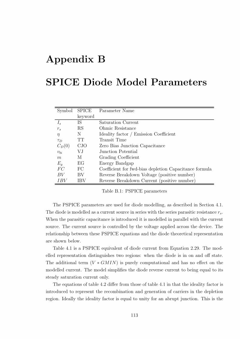
Appendix B
SPICE Diode Model Parameters
Symbol SPICE Parameter Namekeyword
Is IS Saturation Currentrs RS Ohmic Resistanceη N Ideality factor / Emission CoefficientτD TT Transit TimeCD(0) CJO Zero Bias Junction Capacitancevbi VJ Junction Potentialm M Grading CoefficientEg EG Energy BandgapFC FC Coefficient for fwd-bias depletion Capacitance formulaBV BV Reverse Breakdown Voltage (positive number)IBV IBV Reverse Breakdown Current (positive number)
Table B.1: PSPICE parameters
The PSPICE parameters are used for diode modelling, as described in Section 4.1.
The diode is modelled as a current source in series with the series parasitic resistance rs.
When the parasitic capacitance is introduced it is modelled in parallel with the current
source. The current source is controlled by the voltage applied across the device. The
relationship between these PSPICE equations and the diode theoretical representation
are shown below.
Table 4.1 is a PSPICE equivalent of diode current from Equation 2.29. The mod-
elled representation distinguishes two regions: when the diode is in on and off state.
The additional term (V ∗ GMIN) is purely computational and has no effect on the
modelled current. The model simplifies the diode reverse current to being equal to its
steady saturation current only.
The equations of table 4.2 differ from those of table 4.1 in that the ideality factor is
introduced to represent the recombination and generation of carriers in the depletion
region. Ideally the ideality factor is equal to unity for an abrupt junction. This is the
113

same parameter that is introduced in Equation 2.30 in order to show realistic diode
behaviour.
The diode parameter rs takes into account the voltage drop across the diode para-
sitic series resistance. When this parameter is used, the junction voltage is that of the
diode voltage reduced by the voltage drop across the series resistance.
The parameters BV and IBV (used in table 4.3) represent the diode breakdown
voltage and current respectively. The modelled current is set to be equal to the break-
down current at the point when the voltage across the device equals the breakdown
voltage. The PSPICE uses its own representation of the diode current once the bias
voltage exceeds the magnitude of the breakdown voltage.
The diode large signal model takes into consideration its parasitic capacitive effects
generated by the charge storage. The stored charge and the resulting capacitance are
defined by Equations 4.3, 4.4, 4.5 and 4.6. They are clearly determined for the reverse
and low forward bias - as shown in the upper parts of tables 4.4 and 4.5. The behaviour
of the diode junction capacitance at large forward bias is somewhat unclear and there
are various models available to represent this action. The PSPICE uses equations
shown in the lower parts of tables 4.4 and 4.5 to model this effect, as described by [93].
114
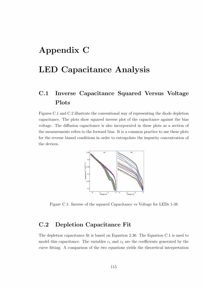
Appendix C
LED Capacitance Analysis
C.1 Inverse Capacitance Squared Versus Voltage
Plots
Figures C.1 and C.2 illustrate the conventional way of representing the diode depletion
capacitance. The plots show squared inverse plot of the capacitance against the bias
voltage. The diffusion capacitance is also incorporated in these plots as a section of
the measurements refers to the forward bias. It is a common practice to use these plots
for the reverse biased conditions in order to extrapolate the impurity concentration of
the devices.
−4 −2 0 2
0.1
0.15
0.2
0.25
0.3
0.35
Voltage [V]
Cap
acita
nce−2
[*10
21F
−2]
(a)
−4 −2 0 2Voltage [V]
(b)
Figure C.1: Inverse of the squared Capacitance vs Voltage for LEDs 1-38
C.2 Depletion Capacitance Fit
The depletion capacitance fit is based on Equation 2.36. The Equation C.1 is used to
model this capacitance. The variables c1 and c2 are the coefficients generated by the
curve fitting. A comparison of the two equations yields the theoretical interpretation
115

−4 −3 −2 −1 0 1 220
25
30
35
40
45
50
55
60
65
70
Voltage [V]
Cap
acita
nce−2
[*10
18F
−2]
Figure C.2: Inverse of the squared Capacitance vs Voltage for LEDs 39 and 40
of the coefficients shown in Equations C.2 and C.3.
Cj = c1
√
1
c2 − V(C.1)
c1 =
√
qǫSNB
2(C.2)
c2 = vbi (C.3)
The results of the depletion capacitance (Equation C.1) fitting to the experimental
data are shown in Figures C.3, C.4, C.5, C.6 and C.7. The fitting procedure that uses
MATLAB unconstrained nonlinear optimisation function (fminsearch) is detailed in
Section 5.1.1.
−4 −3 −2 −1 0 1 2
60
70
80
90
100
110
Voltage [V]
Cap
acita
nce
[pF
]
Figure C.3: Depletion capacitance fit to NO HUMP LEDs
C.3 Diffusion Capacitance Fit
The diffusion capacitance that is caused by the injection of the carriers across the
junction has an exponential shape (as described by Equation 2.43). The model that is
used to represent this capacitance is shown in Equation C.4.
116
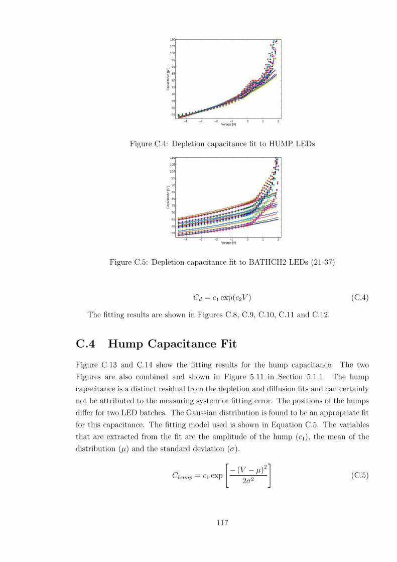
−4 −3 −2 −1 0 1 2
55
60
65
70
75
80
85
90
95
100
105
110
Voltage [V]
Cap
acita
nce
[pF
]
Figure C.4: Depletion capacitance fit to HUMP LEDs
−4 −3 −2 −1 0 1 2
55
60
65
70
75
80
85
90
95
100
105
110
Voltage [V]
Cap
acita
nce
[pF
]
Figure C.5: Depletion capacitance fit to BATHCH2 LEDs (21-37)
Cd = c1 exp(c2V ) (C.4)
The fitting results are shown in Figures C.8, C.9, C.10, C.11 and C.12.
C.4 Hump Capacitance Fit
Figure C.13 and C.14 show the fitting results for the hump capacitance. The two
Figures are also combined and shown in Figure 5.11 in Section 5.1.1. The hump
capacitance is a distinct residual from the depletion and diffusion fits and can certainly
not be attributed to the measuring system or fitting error. The positions of the humps
differ for two LED batches. The Gaussian distribution is found to be an appropriate fit
for this capacitance. The fitting model used is shown in Equation C.5. The variables
that are extracted from the fit are the amplitude of the hump (c1), the mean of the
distribution (µ) and the standard deviation (σ).
Chump = c1 exp
[
− (V − µ)2
2σ2
]
(C.5)
117

−4 −3 −2 −1 0 1 2
55
60
65
70
75
80
85
90
95
100
105
110
Voltage [V]
Cap
acita
nce
[pF
]
Figure C.6: Depletion capacitance fit to LEDs (38)
−4 −3 −2 −1 0 1 2120
130
140
150
160
170
180
190
200
210
Voltage [V]
Cap
acita
nce
[pF
]
Figure C.7: Depletion capacitance fit to LEDs 39 and 40
C.5 Fitting Errors
The fitting errors are the diode capacitance residuals formed when the depletion, junc-
tion and hump capacitance fits are taken away from the experimental measurements.
Figures C.15 and C.17 show the fitting error for the NO-HUMP and BATCH-2 LEDs
on two different scales. The fitting errors for the other groups of LEDs are less stretched
so are shown on a single scale in Figures C.16, C.18 and C.19.
118
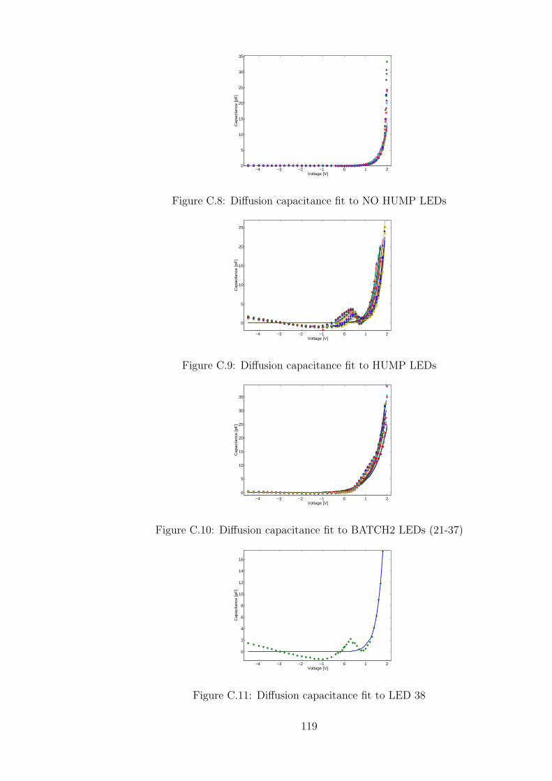
−4 −3 −2 −1 0 1 20
5
10
15
20
25
30
35
Voltage [V]
Cap
acita
nce
[pF
]
Figure C.8: Diffusion capacitance fit to NO HUMP LEDs
−4 −3 −2 −1 0 1 2
0
5
10
15
20
25
Voltage [V]
Cap
acita
nce
[pF
]
Figure C.9: Diffusion capacitance fit to HUMP LEDs
−4 −3 −2 −1 0 1 20
5
10
15
20
25
30
35
Voltage [V]
Cap
acita
nce
[pF
]
Figure C.10: Diffusion capacitance fit to BATCH2 LEDs (21-37)
−4 −3 −2 −1 0 1 2
0
2
4
6
8
10
12
14
16
Voltage [V]
Cap
acita
nce
[pF
]
Figure C.11: Diffusion capacitance fit to LED 38
119

−4 −3 −2 −1 0 1 2
0
5
10
15
20
Voltage [V]
Cap
acita
nce
[pF
]
Figure C.12: Diffusion capacitance fit to LEDs 39 and 40
−4 −3 −2 −1 0 1 2−2
−1
0
1
2
3
4
Voltage [V]
Cap
acita
nce
[pF
]
Figure C.13: Hump capacitance fit to HUMP LEDs
−4 −3 −2 −1 0 1 2−2
−1
0
1
2
3
4
Voltage [V]
Cap
acita
nce
[pF
]
Figure C.14: Hump capacitance fit to BATCH2 LEDs (21-37)
−4 −2 0 2
0
5
10
15
20
Voltage [V]
Cap
acita
nce
[pF
]
(a)
−4 −2 0 2
−0.2
0
0.2
0.4
0.6
0.8
1
1.2
1.4
1.6
1.8
Voltage [V]
(b)
Figure C.15: Capacitance fit error for NO HUMP LEDs
120

−4 −3 −2 −1 0 1 2−2
−1.5
−1
−0.5
0
0.5
1
1.5
2
2.5
3
3.5
Voltage [V]
Cap
acita
nce
[pF
]
Figure C.16: Capacitance fit error for HUMP LEDs
−4 −2 0 2
0
2
4
6
8
10
12
14
Voltage [V]
Cap
acita
nce
[pF
]
(a)
−4 −2 0 2
−1
−0.8
−0.6
−0.4
−0.2
0
0.2
0.4
0.6
0.8
1
Voltage [V]
(b)
Figure C.17: Capacitance fit error for BATCH2 LEDs
−4 −3 −2 −1 0 1 2
−1
−0.5
0
0.5
1
1.5
2
Voltage [V]
Cap
acita
nce
[pF
]
Figure C.18: Capacitance fit error for LED 38
−4 −3 −2 −1 0 1 2
−2
−1.5
−1
−0.5
0
0.5
Voltage [V]
Cap
acita
nce
[pF
]
Figure C.19: Capacitance fit error for LEDs 39 and 40
121

Appendix D
LED Current - Voltage Analysis
Figure D.1 shows the low bias level I-V relationship for the three identified groups of
LEDs. The characteristic is shown on the same scale for the HUMP and NO-HUMP
LEDs. The BATCH-2 LEDs are shown on the same horizontal, but increased vertical
scale. The graphs show the variation in current flowing through the LEDs for the same
voltage applied to the devices. The NO-HUMP LEDs exhibit the lowest current flow
of the three groups of the LEDs. The current flowing through the BATCH-2 LEDs at
the high end of the horizontal scale is by a factor of four larger than of its counterparts
from the other groups.
0
20
40
60
(a)
Cur
rent
[mic
roA
]
0 1 2
0
20
40
60
(b)
Cur
rent
[mic
roA
]
Voltage [V]0 1 2
0
50
100
150
200
250
(c)
Cur
rent
[mic
roA
]
Voltage [V]
Figure D.1: LED low scale I-V relationship: a) NO HUMP, b) HUMP, c) BATCH2
The model of the diode I-V characteristic is represented by Equation A.4. This
relationship is derived from diode practical equation (2.30) as shown in appendix A.2.
The behaviour of this relationship is shown on linear and semi-logarithmic scale in
Figure D.2.
The above fitting equation is rearranged so that the logarithmic value of this re-
122
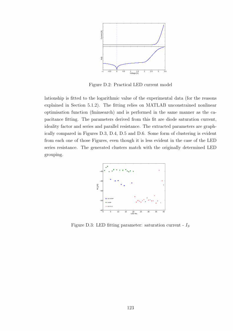
Cur
rent
[A]
−1 −0.5 0 0.5 1 1.5 2 2.5 3 3.5Voltage [V]
ln(I
)
Figure D.2: Practical LED current model
lationship is fitted to the logarithmic value of the experimental data (for the reasons
explained in Section 5.1.2). The fitting relies on MATLAB unconstrained nonlinear
optimisation function (fminsearch) and is performed in the same manner as the ca-
pacitance fitting. The parameters derived from this fit are diode saturation current,
ideality factor and series and parallel resistance. The extracted parameters are graph-
ically compared in Figures D.3, D.4, D.5 and D.6. Some form of clustering is evident
from each one of those Figures, even though it is less evident in the case of the LED
series resistance. The generated clusters match with the originally determined LED
grouping.
0 5 10 15 20 25 30 35 40−60
−55
−50
−45
−40
NO HUMP
HUMP
BATCH 2
LED No.
ln(I
s[A])
Figure D.3: LED fitting parameter: saturation current - IS
123

0 5 10 15 20 25 30 35 40
2
2.5
3
3.5
NO HUMP
HUMP
BATCH 2
LED No.
idea
lity
fact
or −
nFigure D.4: LED fitting parameter: ideality factor - η
0 5 10 15 20 25 30 35 40
28
30
32
34
36
38
40
42
44
46NO HUMP
HUMP
BATCH 2
LED No.
Rs(O
hm)
Figure D.5: LED fitting parameter: series resistance - RS
0 5 10 15 20 25 30 35 407
8
9
10
11
12
7
8
9
10
11
NO HUMP
HUMP
BATCH 2
LED No.
Rp [M
Ohm
]
Figure D.6: LED fitting parameter: series resistance - RP
124

Appendix E
LED Output Spectrum Analysis
The skewness and kurtosis of the LED normalised relative output spectrum are shown
in Figure E.1. There is very little evidence of clustering in this case. Therefore it is
concluded that the skewness and kurtosis of the LED output spectrum are not related
to the previously established device groupings.
0.6
0.8
1
1.2
1.4
1.6
1.8NO HUMP HUMP BATCH 2
skew
ness
(re
lativ
e)
0 5 10 15 20 25 30 35 40
−1
−0.5
0
0.5
1
1.5
LED No.
kurt
osis
(re
lativ
e)
Figure E.1: Skewness and Kurtosis of the LED output spectrum
125

Appendix F
LED Intensity Analysis
Figure F.1 presents the gradients of the linear approximations derived for the LED
relationship between its current and output intensity. The device clustering generated
by the LED output intensity coincides with the previously determined LED groups.
0 5 10 15 20 25 30 35 40
20
25
30
35
40
45
50
NO HUMP
HUMP
BATCH 2
LED No.
grad
ient
[*10
−3 V
]
Figure F.1: Slopes of the fitted current - intensity relationship
126
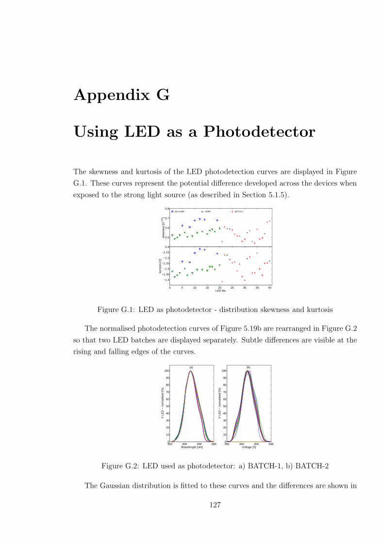
Appendix G
Using LED as a Photodetector
The skewness and kurtosis of the LED photodetection curves are displayed in Figure
G.1. These curves represent the potential difference developed across the devices when
exposed to the strong light source (as described in Section 5.1.5).
0.4
0.5
0.6
0.7
0.8NO HUMP HUMP BATCH 2
skew
ness
[V 0.
5 ]
0 5 10 15 20 25 30 35 40
−1.4
−1.35
−1.3
−1.25
−1.2
−1.15
LED No.
kurt
osis
[V]
Figure G.1: LED as photodetector - distribution skewness and kurtosis
The normalised photodetection curves of Figure 5.19b are rearranged in Figure G.2
so that two LED batches are displayed separately. Subtle differences are visible at the
rising and falling edges of the curves.
350 400 450 5000
10
20
30
40
50
60
70
80
90
100
Wavelength [nm]
V L
ED
− n
orm
alis
ed [%
]
(a)
350 400 450 5000
10
20
30
40
50
60
70
80
90
100
Voltage [V]
V L
ED
− n
orm
alis
ed [%
]
(b)
Figure G.2: LED used as photodetector: a) BATCH-1, b) BATCH-2
The Gaussian distribution is fitted to these curves and the differences are shown in
127

Figure G.3. As predicted from the observation of the curve plots, the BATCH-1 LEDs
have a slight dip in the rising edge of the photodetection curves while the BATCH-2
LEDs have a hump in the same position. Both batches (except LEDs 39 and 40) have
a hump at the falling edge of the curves. It is also noticed that the NO-HUMP LEDs
have narrower spread than it is the case with the other two groups. The Gaussian
distribution is fitted to the residual curves of Figure G.3. A typical fit for each of the
three groups is shown in Figure G.4. The final fitting errors are shown in Figure G.5.
−10
−5
0
5
10
15
erro
r (1
st fi
t)
(a)
350 400 450 500−10
−5
0
5
10
15
Wavelength [nm]
erro
r (1
st fi
t)
(b)
Figure G.3: LED as photodetector - error after first Gaussian fit: a) BATCH-1, b)BATCH-2
350 400 450 5000
10
20
30
40
50
60
70
80
90
100
Wavelength [nm]
V L
ED
(no
rmal
ised
)
*** − measurements
__ − fit
Figure G.4: LED as photodetector - measured data vs complete model: examples LEDs17 (HUMP), 19 (NO-HUMP) and 21(BATCH-2)
128

350 400 450 500−14
−12
−10
−8
−6
−4
−2
0
2
4
Wavelength [nm]
erro
r (c
ompl
ete
fit)
Figure G.5: LED as photodetector - error after complete fit
129
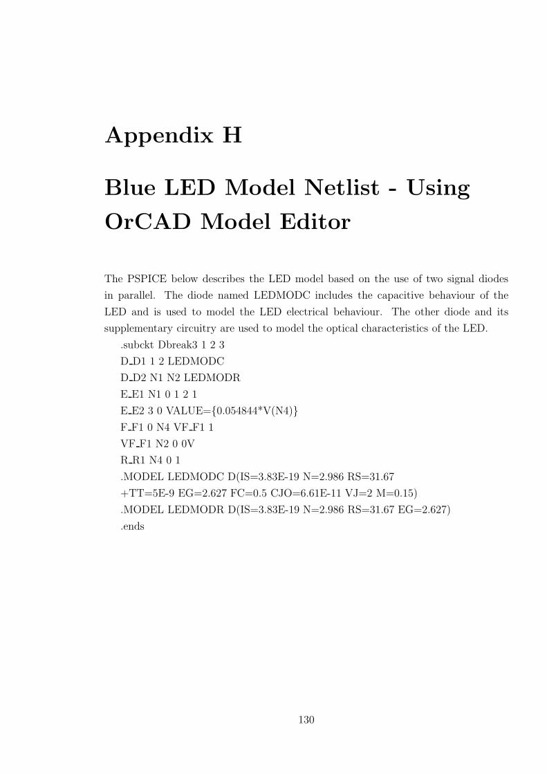
Appendix H
Blue LED Model Netlist - Using
OrCAD Model Editor
The PSPICE below describes the LED model based on the use of two signal diodes
in parallel. The diode named LEDMODC includes the capacitive behaviour of the
LED and is used to model the LED electrical behaviour. The other diode and its
supplementary circuitry are used to model the optical characteristics of the LED.
.subckt Dbreak3 1 2 3
D D1 1 2 LEDMODC
D D2 N1 N2 LEDMODR
E E1 N1 0 1 2 1
E E2 3 0 VALUE=0.054844*V(N4)
F F1 0 N4 VF F1 1
VF F1 N2 0 0V
R R1 N4 0 1
.MODEL LEDMODC D(IS=3.83E-19 N=2.986 RS=31.67
+TT=5E-9 EG=2.627 FC=0.5 CJO=6.61E-11 VJ=2 M=0.15)
.MODEL LEDMODR D(IS=3.83E-19 N=2.986 RS=31.67 EG=2.627)
.ends
130

Bibliography
[1] L F Thompson Cherenkov Ring Imaging and Vector Meson Photoproduction,
University of Sheffield PhD Thesis 1987
[2] J. Carr On behalf of ANTARES Collaboration, Status of ANTARES in Nov 2005,
Nuclear Instruments and Methods in Physics Research A 567 (2006) 428–432
[3] E. Migneco et al., Status of NEMO, Nuclear Instruments and Methods in Physics
Research A567 (2006) 444–451
[4] G. Aggouras et al., Recent results from NESTOR, Nuclear Instruments and Meth-
ods in Physics Research A567 (2006) 452–456
[5] IceCube Collaboration, First year performance of the IceCube neutrino telescope,
Astroparticle Physics 26 (2006) 155–173
[6] V. Aynutdinov et al., BAIKAL experiment: Main results obtained with the neu-
trino telescope NT200, Nuclear Instruments and Methods in Physics Research
A567 (2006) 423–427
[7] U.F. Katz, Neutrino telescopy in the Mediterranean Sea, Progress in Particle and
Nuclear Physics 57 (2006) 273–282
[8] P Amram et al.. (ANTARES collaboration), The ANTARES optical module,
Nuclear Instruments and Methods in Physics Research A484 (2002) 369-383
[9] ANTARES collaboration, Technical Design Report of the
ANTARES 0.1km2 project, (2001) available in pdf at
http://antares.in2p3.fr/Publications/index.html
[10] T Sefzick et al.., A System for Simulation of Scintillator Light Signals, Nuclear
Instruments and Methods in Physics Research A288 (1990) 571-573
[11] W L Reiter and G Stengl, A Blue Light Emitting Diode Used as a Reference
Element in Scintilation Spectrometers, Nuclear Instruments and Methods 180
(1981) 105-157
131
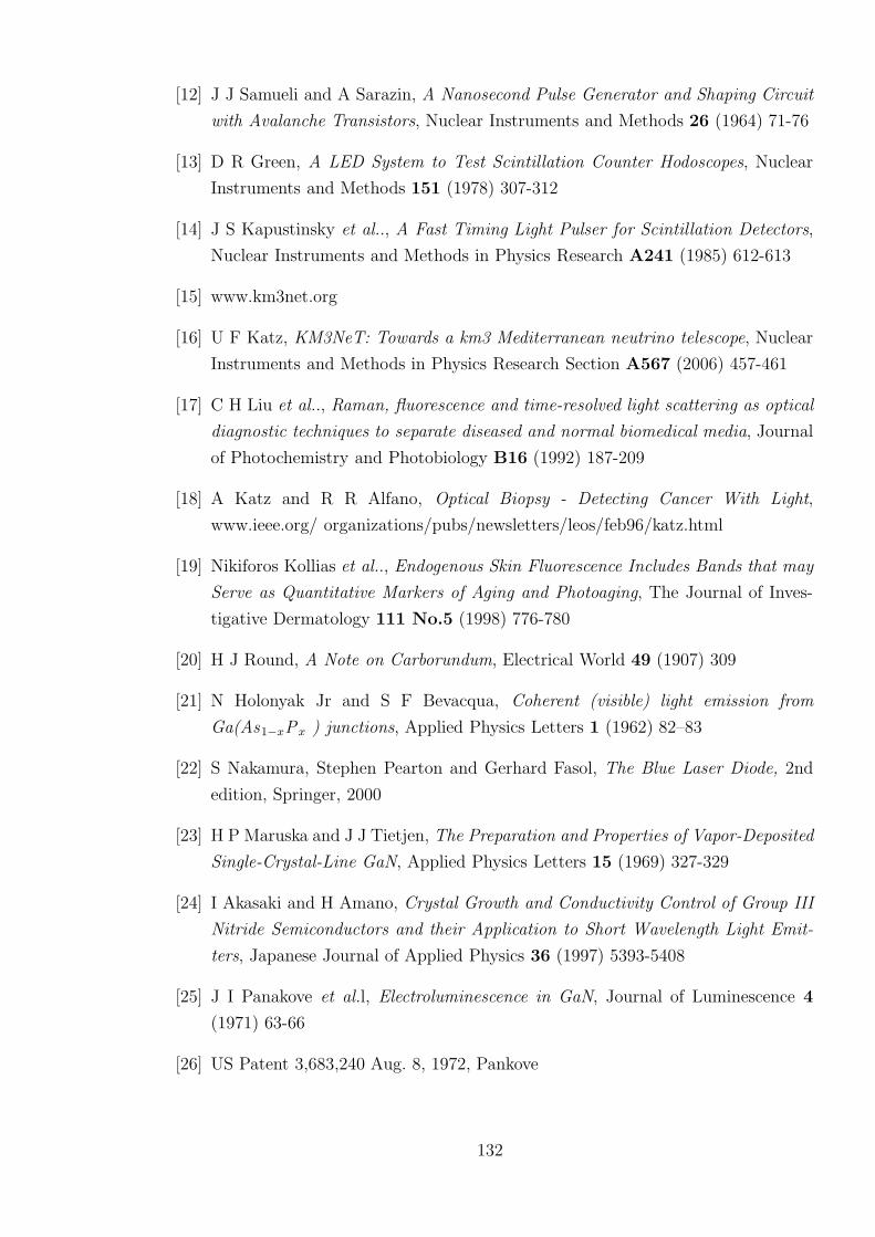
[12] J J Samueli and A Sarazin, A Nanosecond Pulse Generator and Shaping Circuit
with Avalanche Transistors, Nuclear Instruments and Methods 26 (1964) 71-76
[13] D R Green, A LED System to Test Scintillation Counter Hodoscopes, Nuclear
Instruments and Methods 151 (1978) 307-312
[14] J S Kapustinsky et al.., A Fast Timing Light Pulser for Scintillation Detectors,
Nuclear Instruments and Methods in Physics Research A241 (1985) 612-613
[15] www.km3net.org
[16] U F Katz, KM3NeT: Towards a km3 Mediterranean neutrino telescope, Nuclear
Instruments and Methods in Physics Research Section A567 (2006) 457-461
[17] C H Liu et al.., Raman, fluorescence and time-resolved light scattering as optical
diagnostic techniques to separate diseased and normal biomedical media, Journal
of Photochemistry and Photobiology B16 (1992) 187-209
[18] A Katz and R R Alfano, Optical Biopsy - Detecting Cancer With Light,
www.ieee.org/ organizations/pubs/newsletters/leos/feb96/katz.html
[19] Nikiforos Kollias et al.., Endogenous Skin Fluorescence Includes Bands that may
Serve as Quantitative Markers of Aging and Photoaging, The Journal of Inves-
tigative Dermatology 111 No.5 (1998) 776-780
[20] H J Round, A Note on Carborundum, Electrical World 49 (1907) 309
[21] N Holonyak Jr and S F Bevacqua, Coherent (visible) light emission from
Ga(As1−xPx ) junctions, Applied Physics Letters 1 (1962) 82–83
[22] S Nakamura, Stephen Pearton and Gerhard Fasol, The Blue Laser Diode, 2nd
edition, Springer, 2000
[23] H P Maruska and J J Tietjen, The Preparation and Properties of Vapor-Deposited
Single-Crystal-Line GaN, Applied Physics Letters 15 (1969) 327-329
[24] I Akasaki and H Amano, Crystal Growth and Conductivity Control of Group III
Nitride Semiconductors and their Application to Short Wavelength Light Emit-
ters, Japanese Journal of Applied Physics 36 (1997) 5393-5408
[25] J I Panakove et al.l, Electroluminescence in GaN, Journal of Luminescence 4
(1971) 63-66
[26] US Patent 3,683,240 Aug. 8, 1972, Pankove
132

[27] J I Pankove et al., Luminescent properties of GaN, Solid State Communications
8 (1970) 1051-3
[28] H Maruska, W Rhines and D Stevenson, Preparation of Mg-doped GaN diodes
exhibiting violet electroluminescence, Materials Research Bulletin 7 (1972) 777-
781
[29] R Dingle et al., Stimulated Emission and Laser Action in Gallium Nitride, Ap-
plied Physics Letters 19 (1971) 5-7
[30] Y Koide et al., Effect of AlN Buffer Layer on AlGaN/αAl2O3 Heteroepitax-
ial Growth by Metalorganic Vapor Phase Epitaxy, Japanese Journal of Applied
Physics 27 (1988) 1156-1161
[31] US Patent 4,855,249 Aug. 8, 1989, Akasaki et al.
[32] H Amano et al., Metalorganic Vapor Phase Epitaxial Growth of a High Quality
GaN film using an AlN Buffer Layer, Applied Physics Letters 48 (1986) 353-355
[33] S Yoshida, S Misawa and S Gonda , Improvements on the electrical and lumines-
cent properties of reactive molecular beam epitaxially grown GaN films by using
AlN-coated sapphire substrates, Applied Physics Letters, 42 (1983) 427-429
[34] T Nagatomo et al., Propertiesof Ga1−xInxN Films Preparedby MOVPE, Japanese
Journal of Applied Physics 28 (1989) L1334-L1336
[35] K Osamura, S Naka and Y Murakami , Preparation and optical properties of
Ga1xInxN thin films, Journal of Applied Physics 46 (1975) 3432-3437
[36] H Amano et al., P-type Conduction in Mg Doped GaN Treated with Low-Energy
Electron Beam Irradiation (LEEBI), Japanese Journal of Applied Physics 28
(1989) L2112-2114
[37] US Patent 5,334,277 Aug. 2, 1994, Nakamura
[38] S Nakamura, Y Harada and M Seno, Novel Metalorganic Chemical Vapor Depo-
sition for GaN Growth, Applied Physics Letters 58 (1991) 2021-2023
[39] S Nakamura, In Situ Monitoring of GaN Growth Using Interference Effects,
Japanese Journal of Applied Physics 30 (1991) 1620-1627
[40] S Nakamura, GaN Growth Using GaN Buffer Layer, Japanese Journal of Applied
Physics 30 (1991) L1705-L1707
133

[41] S Nakamura, M Senoh and T Mukai, Highly P-typed Mg-Doped GaN Films Grown
with GaN Buffer Layer, Japanese Journal of Applied Physics 30 (1991) L1708-
L1711
[42] S Nakamura, N Mukai and M Senoh, High Power GaN P-N junction Light-
Emitting diodes, Japanese Journal of Applied Physics 30 (1991) L1998-L2001
[43] S Nakamura et al., Thermal Annealing Effects on P-type Mg-doped GaN Films,
Japanese Journal of Applied Physics 31 (1992) L139-L142
[44] S Nakamura et al., Hole Compensation Mechanism of P-type GaN Films,
Japanese Journal of Applied Physics 31 (1992) 1258-1266
[45] C Wang and R Davis, Deposition of highly resistive, undoped, and p-type,
magnesium-doped gallium nitride films by modified gas source molecular beam
epitaxy, Applied Physics Letters 63 (1993) 990-992
[46] S Nakamura T Mukai and M Senoh, Si- and Ge-Doped GaN Films Grown with
GaN Buffer Layers, Japanese Journal of Applied Physics 31 (1992) 2883-2888
[47] W Xie et al., Room temperature blue light emitting p-n diodes from Zn(S,Se)-based
multiple quantum well structures, Applied Physics Letters 60 (1992) 1999-2001
[48] N Yoshimoto et al., Photoluminescence of InGaN films grown at high temperature
by metalorganic vapor phase epitaxy, Applied Physics Letters 59 (1991) 2251-
2253
[49] S Nakamura and T Mukai, High-Quality InGaN Films Grown on GaN Films,
Japanese Journal of Applied Physics 31 (1992) L1457-L1459
[50] S Nakamura, T Mukai and M Senoh, Si-Doped InGaN Films Grown on GaN
Films, Japanese Journal of Applied Physics 32 (1993) L16-L19
[51] S Nakamura, M Senoh and T Mukai, P-GaN / N-InGaN / N-GaN Double Het-
erostructure Blue-Light-Emitting Diodes, Japanese Journal of Applied Physics
32 (1993) L8-L11
[52] S Nakamura, M Senoh and T Mukai High-power lnGaN/GaN double-
heterostructure violet light emitting diodes, Applied Physics Letters 62 (1993)
2390-2392
[53] H Amano et al., Room-temperature violet stimulated emission from optically
pumped AIGaN / GalnN double heterostructure, Applied Physics Letters 64
(1994) 1377-1379
134
[54] S Nakamura, T Mukai and M Senoh , Candela-class high-brightness In-
GaN/AlGaN double heterostructure blue-light-emitting diodes, Applied Physics
Letters 64 (1994) 1687-1689
[55] S Nakamura et al., High-Brightness InGaN Blue, Green and Yellow Light-
Emitting Diodes with Quantum Well Structures, Japanese Journal of Applied
Physics 34 (1995) L797-L799
[56] I Akasaki et al., Stimulated Emission by Current Injection from an AlGaN / GaN
/ GaInN Quantum Well Device, Japanese Journal of Applied Physics 34 (1995)
L1517-L1519
[57] S Nakamura et al., High-power InGaN single-quantum-well-structure blue and
violet light-emitting diodes, Applied Physics Letters 67 (1997) 1868-1870
[58] S Nakamura et al., Superbright Green InGaN Single-Quantum-Well-Structure
Light Emitting Diode, Japanese Journal of Applied Physics 34 (1995) L1332-
L1335
[59] S Kim, H Amano and I Akasaki , Surface-mode stimulated emission from optically
pumped GaInN at room temperature, Applied Physics Letters, 67 (1995) 267-269
[60] S Nakamura et al., InGaN-Based Multi-Quantum-Well-Structure Laser Diodes,
Japanese Journal of Applied Physics 35 (1996) L74-L76
[61] T Mukai, H Narimatsu and S Nakamura, Amber InGaN-Based Light-Emitting
Diodes Operable at High Ambient Temperatures, Japanese Journal of Applied
Physics 37 (1998) L479-L481
[62] T Mukai, M Yamada and S Nakamura, Characteristics of InGaN-Based UV /
Blue / Green / Amber / Red Light-Emitting Diodes, Japanese Journal of Applied
Physics 38 (1999) 3976-3981
[63] T Mukai, M Senoh and S Nakamura, InGaN-Based Blue Light-Emitting Diodes
Grown on Epitaxially Laterally Overgrown GaN Substrates, Japanese Journal of
Applied Physics 37 (1998) L839-L841
[64] T Mukai and S Nakamura, Ultraviolet InGaN and GaN Single Quantum Well
Structure Light Emitting Diodes Grown on Epitaxially Laterally Overgrown GaN
Substrates, Japanese Journal of Applied Physics 38 (1999) 5735-5739
[65] M Yamada et al., Red-Enhanced White-Light-Emitting Diode Using a New Red
Phosphor, Japanese Journal of Applied Physics 42 (2003) L20-L23
135

[66] Y Narukawa et al., Phosphor-Conversion White Light Emitting Diode Using In-
GaN Near-Ultraviolet Chip, Japanese Journal of Applied Physics 41 (2002) L371–
L373
[67] M Iwaya et al., High-Power UV-Light-Emitting Diode on Sapphire, Japanese
Journal of Applied Physics 42 (2003) 400-403
[68] M Razeghi and M Henini, Optoelectronic Devices: III Nitrides, Elsevier 2004
[69] J Kovac, L Paternai and O lengyel, Advanced light emitting diodes structures for
optoelectronic applications, Thin Solid Films 433 (2003) 22-26
[70] M Yamada et al., InGaN-Based Near-Ultraviolet and Blue-Light -Emitting Diodes
with High External Quantum Efficiency Using a Patterned Saphire Substrate and
a Mesh Electrode, Japanese Journal of Applied Physics 41 (2002) L1431-L1433
[71] D Moriata et al., High Output Power 365 nm Ultraviolet Light Emitting Diode of
GaN-Free Structure, Japanese Journal of Applied Physics 41 (2002) L1434-L1436
[72] M Tsukihara et al., Dislocation reduction in GaN layer by introducing GaN-rich
GaNP intermediate layers, Japanese Journal of Applied Physics 42 (2003) 1514-
1516
[73] T Onuma et al., Improved Emission Efficiency in InGaN / GaN Quantum Wells
with Compositionally-Graded Barriers Studied by Time-Resolved Photolumines-
cence Spectroscopy, Japanese Journal of Applied Physics 42 (2003) L1369-L1371
[74] A J Steckl et al., Multiple color capability from rare earth-doped gallium nitride,
Material Science Engineering B81 (2001) 97
[75] M Yamada, Y Narukawa and T Mukai, Phosphor Free High-Luminous- Effi-
ciency White Light-Emitting Diodes Composed of InGaN Multi-Quantum Well,
Japanese Journal of Applied Physics 41 (2002) L1246-L248
[76] ProLight PG1N-5LXS 5W Power LED Technical Datasheet
[77] M Meyyappan and L Kelly, Carbon Nanotubes: Science and Applications, CRC
Press 2004
[78] S V Rotkin and S Subramaney (editors), Applied Physics of Carbon Nanotubes:
Fundamentals of Theory, Optics and Transport Devices, Springer-Verlag 2005
[79] L Pavesi and E V Buzaneva (editors), Frontiers of Nano-Optoelectronic Systems,
Kluwer Academic Publishers 2000
136

[80] J W Plunkett, Plunkett’s Nanotechnology & Mems Industry Almanac 2006, Plun-
kett Research Ltd 2006
[81] P Avouris and J Chen, Nanotube electronics and optoelectronics, Materials Today
9 (2006) 46-54
[82] US Patent 3,172,862 Mar. 9, 1965, E F Gurnee et al.
[83] US Patent 4,356,429 Oct. 26, 1982 C W Tang
[84] US Patent 5,247,190 Sep. 21, 1993 R H Friend, J H Burroughes and D D Bradley
[85] P Le Barny et al., Application of organic electroluminescent materials in visu-
alisation : Electroluminescence organique, Comptes rendus de l’Academie des
sciences. Serie IV, Physique, astrophysique 1 (2000) 493-508
[86] J Kovac, L Peternai and O Lengyel, Advanced Light Emitting Diode Structures
for Optoelectronic Applications, Thin Solid Films 433 (2003) 22-26
[87] L S Hung and C H Chen, Recent progress of molecular organic electroluminescent
materials and devices, Materials Science and Engineering R39 (2002) 143-222
[88] X Xu, G Yu, Y Liu and D Zhu, Electrode modification in organic light-emitting
diodes, Displays 27 (2006) 24-34
[89] D Gubta, M Katiyar and Deepak, Various approaches to white organic light
emitting diodes and their recent advancements, Optical materials 28 (2006) 295-
301
[90] S M Sze, Physics of Semiconductor Devices, 2nd edition, John Willey & Sons,
2002
[91] JM Liu, Photonic Devices, Cambridge university Press, 2005
[92] J Wilson and J Hawkes, Optoelectronics - an introduction, 3rd edition, Prentice
Hall Europe, 1998
[93] G Massobrio & P Antognetti, Device Modelling with SPICE, 2nd Edition,
McGraw-Hill, Inc., 1993
[94] E H Rhoderick and R H Williams, Metal - Semiconductor Contacts, 2nd Edition,
Oxford University Press, 1988
[95] J M Shah et al., Experimental Analysis and Theoretical Model for Anomalously
High Ideality Factors (n>>2.0) in AlGaN/GaN p-n junction diodes, Journal of
Applied Physics 94 (2003) 2627-2630
137
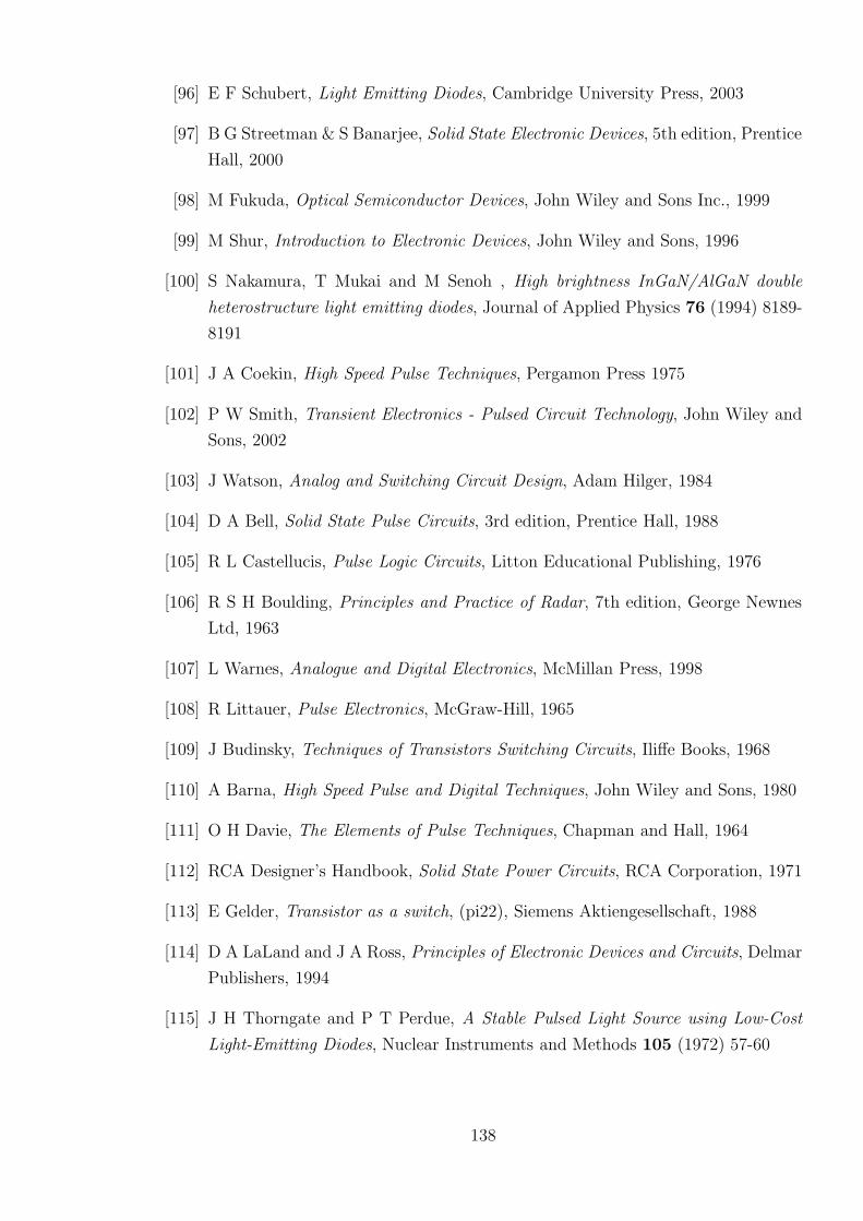
[96] E F Schubert, Light Emitting Diodes, Cambridge University Press, 2003
[97] B G Streetman & S Banarjee, Solid State Electronic Devices, 5th edition, Prentice
Hall, 2000
[98] M Fukuda, Optical Semiconductor Devices, John Wiley and Sons Inc., 1999
[99] M Shur, Introduction to Electronic Devices, John Wiley and Sons, 1996
[100] S Nakamura, T Mukai and M Senoh , High brightness InGaN/AlGaN double
heterostructure light emitting diodes, Journal of Applied Physics 76 (1994) 8189-
8191
[101] J A Coekin, High Speed Pulse Techniques, Pergamon Press 1975
[102] P W Smith, Transient Electronics - Pulsed Circuit Technology, John Wiley and
Sons, 2002
[103] J Watson, Analog and Switching Circuit Design, Adam Hilger, 1984
[104] D A Bell, Solid State Pulse Circuits, 3rd edition, Prentice Hall, 1988
[105] R L Castellucis, Pulse Logic Circuits, Litton Educational Publishing, 1976
[106] R S H Boulding, Principles and Practice of Radar, 7th edition, George Newnes
Ltd, 1963
[107] L Warnes, Analogue and Digital Electronics, McMillan Press, 1998
[108] R Littauer, Pulse Electronics, McGraw-Hill, 1965
[109] J Budinsky, Techniques of Transistors Switching Circuits, Iliffe Books, 1968
[110] A Barna, High Speed Pulse and Digital Techniques, John Wiley and Sons, 1980
[111] O H Davie, The Elements of Pulse Techniques, Chapman and Hall, 1964
[112] RCA Designer’s Handbook, Solid State Power Circuits, RCA Corporation, 1971
[113] E Gelder, Transistor as a switch, (pi22), Siemens Aktiengesellschaft, 1988
[114] D A LaLand and J A Ross, Principles of Electronic Devices and Circuits, Delmar
Publishers, 1994
[115] J H Thorngate and P T Perdue, A Stable Pulsed Light Source using Low-Cost
Light-Emitting Diodes, Nuclear Instruments and Methods 105 (1972) 57-60
138

[116] R V Vasil’ev, B K Lubsandorzhiev and P G Pokhil, A Nanosecond Light Source
for Scintillation and Cherenkov-Detector Calibration, Instruments and Experi-
mental Techniques, 43 (2000) 570-572
[117] J J Samueli and A Sarazin, A Nanosecond Pulse Generator and Shaping Circuit
with Avalanche Transistors, Nuclear Instruments and Methods 26 (1964) 71-76
[118] C C Lo and B Leskovar, A Measuring System for Studying the Time-Resolution
Capabilities of Fast Photomultipliers, IEEE Transactions on Nuclear Science 21
(1977) 93-105
[119] J A Lodge et al., A Cross-Field Photomultiplier with Sub-Nanosecond Risetime
suitable for Nuclear Studies, IEEE Transactions on Nuclear SCience 15 (1968)
491-497
[120] J Millman and H Taub, Pulse, Digital and Switching Waveforms - Devices and
Circuits for their generation and processing, McGraw-Hill, 1965
[121] S Dimitrijev, Understanding Semiconductor Devices, Oxford University Press,
2000
[122] Pulse and Waveform Generation with Step Recovery Diodes, Hewlett Packard
Application Note AN 918
[123] US Patent 4,121,124 Oct. 17, 1978 Hunt
[124] US Patent 3,521,092 Jul. 21, 1970 C H Kalthoff and Boulder
[125] R H Kingston, Switching Time in Junction Diodes and Junction Transistors,
Proceedings of the IRE 42 (1954) 288-293
[126] M L Riaziat, Introduction to high-speed electronics and optoelectronics, John Wil-
ley & Sons, 1996
[127] C M Snowden, Semiconductor Device Modelling, Peter Peregrinus Ltd, 1988
[128] Agilent Sun Power Series HLMP-CB15 InGaN Blue Lamp - Data Sheet
[129] Marconi TF 1313A 0.1% Universal Bridge - Instruction Manual
[130] E Kreyszig Advanced Engineering Mathematics, 7th edition, John Willey and
Sons, 1993
[131] J C Lagarias, J A Reeds, M H Wright and P E Wright Convergence Proper-
ties of the Nelder-Mead Simplex Method in Low Dimensions SIAM Journal of
Optimization 9 (1998) 112-147
139
[132] C Van Opdrop and H K J Kanerva Current - Voltage Characteristics and Ca-
pacitance of Isotype heterojunctions Solid-State Electronics 10 (1967) 401-421
[133] S Luryi Quantum Capacitance Devices Applied Physics Letters 52 (1988) 501-503
[134] G J Borse Numerical Methods with MATLAB, An International Thompson Pub-
lishing Company, 1997
[135] Spectrometer Control And Data Acquisition System - Datasheet
[136] E Miyazaki, S Itami and T Araki, Using a light-emitting diode as a high-speed,
wavelength selective photodetector, Review of Scientific Instruments 69 (1998)
3751-3754
[137] L Euler, De serie Lambertina plurimiscue eius insignibus proprietatibus, Acta
Academiae Scientiarum Petropolitanae 2 (1783) 29-51
[138] E Anderson et al., LAPACK User’s Guide
(www.netlib.org/lapack/lug/lapack lug.html), 3rd edition, SIAM, 1999
[139] Gate Drive Design for Large Drive MOSFETs, Advanced Power Technology Ap-
plication Note APT 9302
[140] H W Johnson and M Graham High Speed Digital Design; a Handbook of Black
Magic, New Jersey: Prentice Hall, 1993
[141] L M Bollinger and G E Thomas Measurement of the Time Dependence of Scin-
tillation Intensity by a Delayed-Coincidence Method Review of Scientific Instru-
ments 32 (1961) 1044-1050
[142] J E McMillan The single photon technique for measuring LED pulser flash width
Sheffield Particle Astrophysics (Sheffield University – Department of Physics and
Astronomy Internal Publication) (1999) SH-HEP-99-07
[143] http://mathworld.wolfram.com/LambertW-Function.html
[144] T C Banwell and A Jayakumar, Exact analytical solution for current flow through
diode with series resistance, Electronics Letters 36 (2000) 291-292
[145] A Ortiz-Conde, F J Garcia Sanchez, Extraction of non-ideal junction model pa-
rameters from the explicit analytic solutions of its I–V characteristics, Solid State
Electronics 49 (2005) 465-472
[146] A Jain and A Kapoor, Exact analytical solutions of the parameters of real solar
cells using Lambert W-function, Solar Energy Materials & Solar Cells 81 (2004)
269–277
140

[147] A Ortiz-Conde, F J Garcıa Sanchez and J Muci, Exact analytical solutions of
the forward non-ideal diode equation with series and shunt parasitic resistances
- Technical Note, Solid-State Electronics 44 (2000) 1861-1864
141