Sub-nanosecond switching and acceleration to relativistic ...
4
Sub-nanosecond switching and acceleration to relativistic energies of field emission electron bunches from metallic nano-tips S. Tsujino, 1,a) M. Paraliev, 2 E. Kirk, 1 C. Gough, 2 S. Ivkovic, 2 and H.-H. Braun 3 1 Laboratory for Micro- and Nanotechnology, Department of Synchrotron Radiation and Nanotechnology, Paul Scherrer Institut, CH-5232 Villigen-PSI, Switzerland 2 Department of Large Scale Research Facilities, Paul Scherrer Institut, CH-5232 Villigen-PSI, Switzerland 3 SwissFEL, Paul Scherrer Institut, CH-5232 Villigen-PSI, Switzerland (Received 18 April 2011; accepted 4 May 2011; published online 10 June 2011) The authors explore the generation of short electron bunches from a field-emitter array cathode consisting of nanometer-sized metallic tips that is compatible with an acceleration electric field above 10 MV/m. Sub-nanosecond field emission electron bunches were generated by applying fast electrical pulses to an on-chip electron extraction gate electrode of the cathode. The subsequent acceleration of the field emission electron bunches to 5 MeV was demonstrated using the combined diode-RF cavity SwissFEL electron gun test facility. V C 2011 American Institute of Physics. [doi:10.1063/1.3594579] The high current density and high brightness of field emission beams 1–3 have motivated the use of field emitters as electron sources in applications such as microwave ampli- fiers 4–8 and free electron lasers. 2,3,9–18 For the anticipated current densities, a high acceleration gradient is important to preserve the beam emittance. Nano-fabricated field emitter array (FEA) cathodes, equipped with nanometer-scale sharp tips and an on-chip electron extraction gate electrode, are well-suited for this purpose, owing to partial electrostatic shielding of individual field emitters from the accelerating field by the gate electrode, and the capability of switching the electron emission independently from the accelerating field. Recently, the switching of a field-emission electron beam from a FEA on a time scale of a few nanoseconds and up to 300 keV acceleration of the field-emission electron beam by a diode-gun accelerator was reported. 18 In this work, we show field emission current switching for sub- nanosecond electron bunch generation and the combination of the method with a diode-radio frequency (RF) cavity elec- tron gun to generate field-emission electron beam with rela- tivistic energies. The single-gate FEA cathodes (Fig. 1) were fabricated by molding and a self-aligned gate process. 15 They consist of 1.2 10 5 pyramidal shape molybdenum field emitter tips 1.2 lm in height and a 1.5 lm base size, aligned with 5 lm spacing on a 0.3 mm thick electroplated nickel substrate. The electron emission is switched on by applying a negative volt- age pulse, –V em , to the field emitters with respect to the elec- tron extraction gate electrode, which has 2 lm diameter apertures for individual emitters. The gate electrode is a 0.5- lm-thick molybdenum film separated from the emitter sub- strate by a 1.2-lm-thick SiO 2 film, and is patterned to a 5.4- mm-diameter circular shape. The gate-electrode diameter here is required to apply a large accelerating electric field above 10 MV/m. 18 Consequently, it leads to an increased capacitance, C g , between the gate electrode and the field emitter substrate. To partly compensate for the capacitance increase, we inserted a 1.2-lm-thick SiON film underneath the SiO 2 layer outside the emitter array area, as shown in Fig. 1(b). The resulting C g was 0.5 nF. This is an order of magnitude larger than that of a Spindt FEA used for the RF emission-gate experiment 7 due to the larger gate electrode area. However, the RC con- stant of our all-metallic FEAs is several orders of magnitude below 1 ns, since the resistance of the substrate is low. 18 Hence, it is possible to switch V em in 1 ns [in full width at half maximum (FWHM)] by using the following method [cf., Figs. 1(c) and 1(d)]: first we apply a negative current pulse to the emitter substrate with the FWHM-duration, T p , below 1 ns, with the amplitude determined by C g V em /T p ; then we apply a second current pulse with positive polarity, and with the same duration and amplitude, delayed by DT of 1 ns from the first pulse. As a result, combined with the non- linear current-voltage characteristics of the field emission, 7 we expect to be able to produce a field emission current pulse with sub-nanosecond duration. In the experiment described in the following text, we used current pulses with T p of 0.65 ns. We also adjusted V em by applying a dc bias, V dc , in series to the double current pulses. The electron bunch acceleration experiment used the combined diode-RF cavity gun [Fig. 1(c)] of the SwissFEL test facility at the Paul Scherrer Institut. In the diode gun, a pulsed cathode voltage up to 500 kV with 250 ns duration (FWHM) and a maximum repetition frequency of 10 Hz can be applied by using the critically coupled air-core trans- former technology. 19 After passing through the anode iris, the electron bunch is transported to a 2-cell RF-cavity through a 150 mm tunnel and further accelerated by a 1.49896 GHz RF-field. 20 The electron beam is detected ei- ther by one of the scintillating screen monitors or by a Fara- day cup. The energy of the accelerated electron beam can be measured by dispersing the beam using a dipole magnet located 3 m downstream of the beam line, and imaging it on a screen monitor. a) Author to whom correspondence should be addressed. Electronic mail: [email protected]. 1070-664X/2011/18(6)/064502/4/$30.00 V C 2011 American Institute of Physics 18, 064502-1 PHYSICS OF PLASMAS 18, 064502 (2011) Downloaded 24 Aug 2011 to 192.33.126.162. Redistribution subject to AIP license or copyright; see http://pop.aip.org/about/rights_and_permissions
Transcript of Sub-nanosecond switching and acceleration to relativistic ...
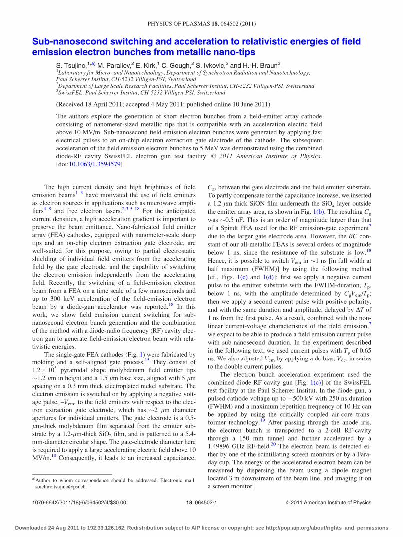
Sub-nanosecond switching and acceleration to relativistic energies of fieldemission electron bunches from metallic nano-tips
S. Tsujino,1,a) M. Paraliev,2 E. Kirk,1 C. Gough,2 S. Ivkovic,2 and H.-H. Braun3
1Laboratory for Micro- and Nanotechnology, Department of Synchrotron Radiation and Nanotechnology,Paul Scherrer Institut, CH-5232 Villigen-PSI, Switzerland2Department of Large Scale Research Facilities, Paul Scherrer Institut, CH-5232 Villigen-PSI, Switzerland3SwissFEL, Paul Scherrer Institut, CH-5232 Villigen-PSI, Switzerland
(Received 18 April 2011; accepted 4 May 2011; published online 10 June 2011)
The authors explore the generation of short electron bunches from a field-emitter array cathode
consisting of nanometer-sized metallic tips that is compatible with an acceleration electric field
above 10 MV/m. Sub-nanosecond field emission electron bunches were generated by applying fast
electrical pulses to an on-chip electron extraction gate electrode of the cathode. The subsequent
acceleration of the field emission electron bunches to 5 MeV was demonstrated using the combined
diode-RF cavity SwissFEL electron gun test facility. VC 2011 American Institute of Physics.
[doi:10.1063/1.3594579]
The high current density and high brightness of field
emission beams1–3 have motivated the use of field emitters
as electron sources in applications such as microwave ampli-
fiers4–8 and free electron lasers.2,3,9–18 For the anticipated
current densities, a high acceleration gradient is important to
preserve the beam emittance. Nano-fabricated field emitter
array (FEA) cathodes, equipped with nanometer-scale sharp
tips and an on-chip electron extraction gate electrode, are
well-suited for this purpose, owing to partial electrostatic
shielding of individual field emitters from the accelerating
field by the gate electrode, and the capability of switching
the electron emission independently from the accelerating
field. Recently, the switching of a field-emission electron
beam from a FEA on a time scale of a few nanoseconds and
up to 300 keV acceleration of the field-emission electron
beam by a diode-gun accelerator was reported.18 In this
work, we show field emission current switching for sub-
nanosecond electron bunch generation and the combination
of the method with a diode-radio frequency (RF) cavity elec-
tron gun to generate field-emission electron beam with rela-
tivistic energies.
The single-gate FEA cathodes (Fig. 1) were fabricated by
molding and a self-aligned gate process.15 They consist of
1.2� 105 pyramidal shape molybdenum field emitter tips
�1.2 lm in height and a 1.5 lm base size, aligned with 5 lm
spacing on a 0.3 mm thick electroplated nickel substrate. The
electron emission is switched on by applying a negative volt-
age pulse, –Vem, to the field emitters with respect to the elec-
tron extraction gate electrode, which has �2 lm diameter
apertures for individual emitters. The gate electrode is a 0.5-
lm-thick molybdenum film separated from the emitter sub-
strate by a 1.2-lm-thick SiO2 film, and is patterned to a 5.4-
mm-diameter circular shape. The gate-electrode diameter here
is required to apply a large accelerating electric field above 10
MV/m.18 Consequently, it leads to an increased capacitance,
Cg, between the gate electrode and the field emitter substrate.
To partly compensate for the capacitance increase, we inserted
a 1.2-lm-thick SiON film underneath the SiO2 layer outside
the emitter array area, as shown in Fig. 1(b). The resulting Cg
was �0.5 nF. This is an order of magnitude larger than that
of a Spindt FEA used for the RF emission-gate experiment7
due to the larger gate electrode area. However, the RC con-
stant of our all-metallic FEAs is several orders of magnitude
below 1 ns, since the resistance of the substrate is low.18
Hence, it is possible to switch Vem in �1 ns [in full width at
half maximum (FWHM)] by using the following method
[cf., Figs. 1(c) and 1(d)]: first we apply a negative current
pulse to the emitter substrate with the FWHM-duration, Tp,
below 1 ns, with the amplitude determined by CgVem/Tp;
then we apply a second current pulse with positive polarity,
and with the same duration and amplitude, delayed by DT of
1 ns from the first pulse. As a result, combined with the non-
linear current-voltage characteristics of the field emission,7
we expect to be able to produce a field emission current pulse
with sub-nanosecond duration. In the experiment described
in the following text, we used current pulses with Tp of 0.65
ns. We also adjusted Vem by applying a dc bias, Vdc, in series
to the double current pulses.
The electron bunch acceleration experiment used the
combined diode-RF cavity gun [Fig. 1(c)] of the SwissFEL
test facility at the Paul Scherrer Institut. In the diode gun, a
pulsed cathode voltage up to �500 kV with 250 ns duration
(FWHM) and a maximum repetition frequency of 10 Hz can
be applied by using the critically coupled air-core trans-
former technology.19 After passing through the anode iris,
the electron bunch is transported to a 2-cell RF-cavity
through a 150 mm tunnel and further accelerated by a
1.49896 GHz RF-field.20 The electron beam is detected ei-
ther by one of the scintillating screen monitors or by a Fara-
day cup. The energy of the accelerated electron beam can be
measured by dispersing the beam using a dipole magnet
located 3 m downstream of the beam line, and imaging it on
a screen monitor.
a)Author to whom correspondence should be addressed. Electronic mail:
1070-664X/2011/18(6)/064502/4/$30.00 VC 2011 American Institute of Physics18, 064502-1
PHYSICS OF PLASMAS 18, 064502 (2011)
Downloaded 24 Aug 2011 to 192.33.126.162. Redistribution subject to AIP license or copyright; see http://pop.aip.org/about/rights_and_permissions
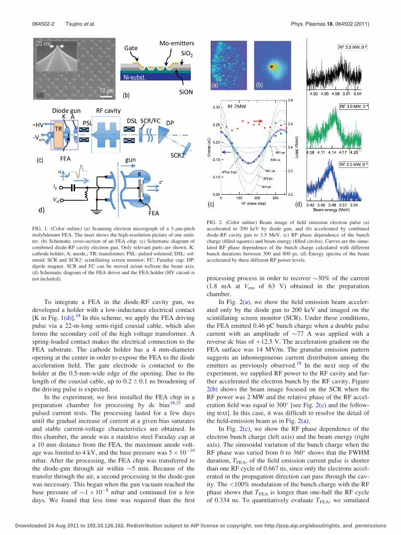
To integrate a FEA in the diode-RF cavity gun, we
developed a holder with a low-inductance electrical contact
[K in Fig. 1(d)].18 In this scheme, we apply the FEA driving
pulse via a 22-m-long semi-rigid coaxial cable, which also
forms the secondary coil of the high voltage transformer. A
spring-loaded contact makes the electrical connection to the
FEA substrate. The cathode holder has a 4 mm-diameter
opening at the center in order to expose the FEA to the diode
acceleration field. The gate electrode is contacted to the
holder at the 0.5-mm-wide edge of the opening. Due to the
length of the coaxial cable, up to 0.2 6 0.1 ns broadening of
the driving pulse is expected.
In the experiment, we first installed the FEA chip in a
preparation chamber for processing by dc bias18,21 and
pulsed current tests. The processing lasted for a few days
until the gradual increase of current at a given bias saturates
and stable current-voltage characteristics are obtained. In
this chamber, the anode was a stainless steel Faraday cup at
a 10 mm distance from the FEA, the maximum anode volt-
age was limited to 4 kV, and the base pressure was 5� 10�10
mbar. After the processing, the FEA chip was transferred to
the diode-gun through air within �5 min. Because of the
transfer through the air, a second processing in the diode-gun
was necessary. This began when the gun vacuum reached the
base pressure of �1� 10�8 mbar and continued for a few
days. We found that less time was required than the first
processing process in order to recover �30% of the current
(1.8 mA at Vem of 63 V) obtained in the preparation
chamber.
In Fig. 2(a), we show the field emission beam acceler-
ated only by the diode gun to 200 keV and imaged on the
scintillating screen monitor (SCR). Under these conditions,
the FEA emitted 0.46 pC bunch charge when a double pulse
current with an amplitude of �77 A was applied with a
reverse dc bias of þ12.5 V. The acceleration gradient on the
FEA surface was 14 MV/m. The granular emission pattern
suggests an inhomogeneous current distribution among the
emitters as previously observed.18 In the next step of the
experiment, we supplied RF power to the RF cavity and fur-
ther accelerated the electron bunch by the RF cavity. Figure
2(b) shows the beam image focused on the SCR when the
RF power was 2 MW and the relative phase of the RF accel-
eration field was equal to 300� [see Fig. 2(c) and the follow-
ing text]. In this case, it was difficult to resolve the detail of
the field-emission beam as in Fig. 2(a).
In Fig. 2(c), we show the RF phase dependence of the
electron bunch charge (left axis) and the beam energy (right
axis). The sinusoidal variation of the bunch charge when the
RF phase was varied from 0 to 360� shows that the FWHM
duration, TFEA, of the field emission current pulse is shorter
than one RF cycle of 0.667 ns, since only the electrons accel-
erated in the propagation direction can pass through the cav-
ity. The <100% modulation of the bunch charge with the RF
phase shows that TFEA is longer than one-half the RF cycle
of 0.334 ns. To quantitatively evaluate TFEA, we simulated
FIG. 2. (Color online) Beam image of field emission electron pulse (a)
accelerated to 200 keV by diode gun, and (b) accelerated by combined
diode-RF cavity gun to 3.5 MeV. (c) RF phase dependence of the bunch
charge (filled squares) and beam energy (filled circles). Curves are the simu-
lated RF phase dependence of the bunch charge calculated with different
bunch durations between 300 and 800 ps. (d) Energy spectra of the beam
accelerated by three different RF power levels.
FIG. 1. (Color online) (a) Scanning electron micrograph of a 5-lm-pitch
molybdenum FEA. The inset shows the high-resolution picture of one emit-
ter. (b) Schematic cross-section of an FEA chip. (c) Schematic diagram of
combined diode-RF cavity electron gun. Only relevant parts are shown. K:
cathode holder; A: anode,; TR: transformer; PSL: pulsed solenoid; DSL: sol-
enoid; SCR and SCR2: scintillating screen monitor; FC: Faraday cup; DP:
dipole magnet. SCR and FC can be moved in/out to/from the beam axis.
(d) Schematic diagram of the FEA driver and the FEA holder (HV circuit is
not included).
064502-2 Tsujino et al. Phys. Plasmas 18, 064502 (2011)
Downloaded 24 Aug 2011 to 192.33.126.162. Redistribution subject to AIP license or copyright; see http://pop.aip.org/about/rights_and_permissions
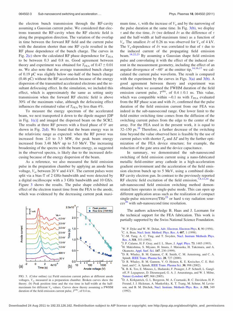
the electron bunch transmission through the RF-cavity
assuming a Gaussian current pulse. We considered that elec-
trons transmit the RF-cavity when the RF electric field is
along the propagation direction. The variation of the overlap
in time between the forward RF field and the current pulse
with the duration shorter than one RF cycle resulted in the
RF phase dependence of the bunch charge. The curves in
Fig. 2(c) show the calculated RF phase dependence for TFEA
to be between 0.3 and 0.8 ns. Good agreement between
theory and experiment was obtained for TFEA of 0.47 6 0.01
ns. We also note that the average transmitted bunch charge
of 0.19 pC was slightly below one-half of the bunch charge
(0.46 pC) without the RF acceleration because of the energy
dispersion of the transmitted accelerated electrons and the re-
sultant defocusing effect. In the simulation, we included this
effect, which is approximately the same as setting unity
transmission when the forward RF electric field is above
30% of the maximum value, although the defocusing effect
influences the estimated value of TFEA by less than 4%.
To measure the energy spectrum of the accelerated
beam, we next transported it down to the dipole magnet [DP
in Fig. 1(c)] and imaged the dispersed beam on the SCR2.
The results at three RF powers with a fixed phase of 0� are
shown in Fig. 2(d). We found that the beam energy was in
the relativistic range as expected: when the RF power was
increased from 2.0 to 3.5 MW, the peak beam energy
increased from 3.48 MeV up to 5.0 MeV. The increasing
broadening of the spectra with the beam energy, as suggested
in the observed spectra, is likely due to the increased defo-
cusing because of the energy dispersion of the beam.
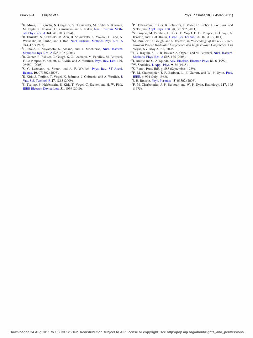
As a reference, we also measured the field emission
pulse in the preparation chamber by applying an anode bias
voltage, Va, between 20 V and 4 kV. The current pulses were
split via a bias-T of 2 GHz-bandwidth and were detected by
a digital oscilloscope with a 3 GHz bandwidth and 10 GS/s.
Figure 3 shows the results. The pulse shape exhibited an
effect of the electron transit time from the FEA to the anode,
which was evidenced by the decreasing current peak maxi-
mum time, s, with the increase of Va and by the narrowing of
the pulse duration at the same time. In Fig. 3(b), we display
s and the rise time, ds (we defined ds as the difference of sand the half-width at half-maximum time) as a function of
Va. The smallest ds of 0.26 ns was observed for Va of 4 kV.
The Va-dependence of ds was correlated to that of s due to
the induced current of the propagating field emission
beam.18,22,23 By assuming a Gaussian shape field emission
pulse and convoluting it with the effect of the induced cur-
rent in the measurement geometry, including the effect of an
angular divergence of �60� at the emitter tip,14,16,17 we cal-
culated the current pulse waveform. The result is compared
with the experiment by the curves in Figs. 3(a) and 3(b). A
good agreement between theory and experiment was
obtained when we assumed the FWHM duration of the field
emission current pulse, T(th), of 0.4 6 0.1 ns. This value,
which was compatible within �0.1 ns with TFEA evaluated
from the RF phase scan and with ds, confirmed that the pulse
duration of the field emission current from our FEA was
indeed in the sub-nanosecond range. One lower limit to the
field emitter switching time comes from the diffusion of the
switching current pulses from the edge to the center of the
array. For the FEA used in the present work, it is equal to
32–150 ps.18 Therefore, a further decrease of the switching
time beyond the value observed here is feasible by the use of
current pulses with shorter Tp and DT and by the further opti-
mization of the FEA device structure; for example, the
reduction of the gate area and the device capacitance.
In summary, we demonstrated the sub-nanosecond
switching of field emission current using a nano-fabricated
metallic field-emitter array cathode in a high-acceleration
gradient environment and the acceleration of the field emis-
sion electron bunch up to 5 MeV, using a combined diode-
RF cavity electron gun. In contrast to the previously reported
RF electric field excitation of the field emission,7,8,12,24 the
sub-nanosecond field emission switching method demon-
strated here operates in single-pulse mode. This can open up
different application areas such as the realization of compact
single-pulse microwave/THz25 or hard x-ray radiation sour-
ces26 with sub-nanosecond time resolution.
The authors acknowledge B. Haas and J. Leemann for
the technical support for the FEA fabrication. This work is
partially supported by the Swiss National Science Foundation.
1W. P. Dyke and W. W. Dolan, Adv. Electron. Electron Phys. 8, 90 (1956).2C. A. Brau, Nucl. Instr. Method. Phys. Res. A 407, 1 (1998).3C.-M. Tang, A. C. Ting, and T. Swyden, Nucl. Instrum Methods Phys.
Res. A 318, 353 (1992).4J. P. Calame, H. F. Gray, and J. L. Shaw, J. Appl. Phys. 73, 1485 (1993).5H. Makishima, S. Miyano, H. Imura, J. Matsuoka, H. Takemura, and A.
Okamoto, Appl. Surf. Sci. 147, 230 (1999).6D. R. Whaley, B. M. Gannon, C. R. Smith, C. M. Armstrong, and C. A.
Spindt, IEEE Trans. Plasma Sci. 28, 727 (2000).7D. R. Whaley, B. M. Gannon, V. O. Heinen, K. E. Kreischer, C. E. Hol-
land, and C. A. Spindt, IEEE Trans. Plasma Sci. 30, 998 (2002).8K. B. K. Teo, E. Minoux, L. Hudanski, F. Peauger, J.-P. Schnell, L. Gangl-
off, P. Legagneux, D. Dieumegard, G. A. J. Amaratunga, and W. I. Milne,
Nature (London) 437, 968 (2005).9D. A. Kirkpatrick, G. L. Bergeron, M. A. Czarnaski, R. C. Davidson, H. P.
Freund, J. J. Hickman, A. Mankofsky, K. T. Tsang, M. Schnur, M. Levin-
son, and B. M. Ditchek, Nucl. Instrum. Methods Phys. Res. A 318, 349
(1992).
FIG. 3. (Color online) (a) Field emission current pulses at different anode
voltages, Va, measured in a preparation chamber. Broken curves show the
theory. (b) Peak position time and the rise time in half-width at the half-
maximum for different Va values. Curves show theory assuming a FWHM
duration of the field emission current pulse, T(th), of 0.4 ns.
064502-3 Sub-nanosecond switching and acceleration … Phys. Plasmas 18, 064502 (2011)
Downloaded 24 Aug 2011 to 192.33.126.162. Redistribution subject to AIP license or copyright; see http://pop.aip.org/about/rights_and_permissions
10K. Mima, T. Taguchi, N. Ohigashi, Y. Tsunawaki, M. Shiho, S. Kuruma,
M. Fujita, K. Imasaki, C. Yamanaka, and S. Nakai, Nucl. Instrum. Meth-
ods Phys. Res. A 341, AB 103 (1994).11H. Ishizuka, S. Kawasaki, M. Arai, H. Shimawaki, K. Yokoo, H. Kubo, A.
Watanabe, M. Shiho, and J. Itoh, Nucl. Instrum. Methods Phys. Res. A
393, 479 (1997).12T. Inoue, S. Miyamoto, S. Amano, and T. Mochizuki, Nucl. Instrum.
Methods Phys. Res. A 528, 402 (2004).13R. Ganter, R. Bakker, C. Gough, S. C. Leemann, M. Paraliev, M. Pedrozzi,
F. Le Pimpec, V. Schlott, L. Rivkin, and A. Wrulich, Phys. Rev. Lett. 100,
064801 (2008).14S. C. Leemann, A. Streun, and A. F. Wrulich, Phys. Rev. ST Accel.
Beams. 10, 071302 (2007).15E. Kirk, S. Tsujino, T. Vogel, K. Jefimovs, J. Gobrecht, and A. Wrulich, J.
Vac. Sci. Technol. B 27, 1813 (2009).16S. Tsujino, P. Helfenstein, E. Kirk, T. Vogel, C. Escher, and H.-W. Fink,
IEEE Electron Device Lett. 31, 1059 (2010).
17P. Helfenstein, E. Kirk, K. Jefimovs, T. Vogel, C. Escher, H.-W. Fink, and
S. Tsujino, Appl. Phys. Lett. 98, 061502 (2011).18S. Tsujino, M. Paraliev, E. Kirk, T. Vogel. F. Le Pimpec, C. Gough, S.
Ivkovic, and H.-H. Braun, J. Vac. Sci. Technol. 29, 02B117 (2011).19M. Paraliev, C. Gough, and S. Ivkovic, in Proceedings of the IEEE Inter-
national Power Modulator Conference and High Voltage Conference, Las
Vegas, NV, May 27-31, 2008.20J.-Y. Raguin, K. Li, R. Bakker, A. Oppelt, and M. Pedrozzi, Nucl. Instrum.
Methods. Phys. Res. A 593, 125 (2008).21I. Brodie and C. A. Spindt, Adv. Electron. Electron Phys. 83, 6 (1992).22W. Shockley, J. Appl. Phys. 9, 35 (1938).23S. Ramo, Proc. IRE, p. 583 (September, 1939).24F. M. Charbonnier, J. P. Barbour, L. F. Garrett, and W. P. Dyke, Proc.
IEEE, p. 991 (July, 1963).25J. H. Booske, Phys. Plasmas. 15, 05502 (2008).26F. M. Charbonnier, J. P. Barbour, and W. P. Dyke, Radiology. 117, 165
(1975).
064502-4 Tsujino et al. Phys. Plasmas 18, 064502 (2011)
Downloaded 24 Aug 2011 to 192.33.126.162. Redistribution subject to AIP license or copyright; see http://pop.aip.org/about/rights_and_permissions