Circuit Board Design Preface - Freedunet.nicolas.free.fr/CATIAV5/cbdug.pdfUsing This Guide This...
108
Circuit Board Design Preface What's New Getting Started Basic Tasks Advanced Tasks Workbench Description Glossary Index © Dassault Systèmes 1994-2000. All rights reserved. TOC file:///E|/Www/ADGdocR5/CbdEnglish/cbdug.doc/src/cbdugtoc.htm [09/26/2000 13:47:57]
Transcript of Circuit Board Design Preface - Freedunet.nicolas.free.fr/CATIAV5/cbdug.pdfUsing This Guide This...

Circuit Board Design
Preface
What's New
Getting Started
Basic Tasks
Advanced Tasks
Workbench Description
Glossary
Index
© Dassault Systèmes 1994-2000. All rights reserved.
TOC
file:///E|/Www/ADGdocR5/CbdEnglish/cbdug.doc/src/cbdugtoc.htm [09/26/2000 13:47:57]

PrefaceThe CATIA Version 5 Circuit Board Design is a new generation product which addresses circuitboard design in a mechanical design context and interfaces with industry standard ECADsystems.
The CATIA - Circuit Board Design offers the following main functions:Data can be exchanged with ECAD Systems through IDF Files (import/export)Circuit board geometry is designed within the global assembly product definitiontaking into account the mechanical contextElectronic properties such as top and bottom faces can be defined and editedon any parts and assembliesSpatial and technological constraint areas can be created and managedCircuit board definitions can be analyzed in the context of the full Digital Mock-UpdefinitionCreation and management of electronic part catalogs are availableHole and cutout patterns are supportedJournaling and report capabilities.
As a scalable product, CATIA Version 5 Circuit Board Design can be used in cooperation withother current or future companion products of the next CATIA generation such as CATIAVersion 5 Assembly Design and ENOVIA-DMU Navigator Version 5.
Using This GuideMore Information
Preface
file:///E|/Www/ADGdocR5/CbdEnglish/cbdug.doc/src/cbdugpr01.htm [09/26/2000 13:48:01]
Using This GuideThis guide is intended for the user who needs to become quickly familiar with the CATIA -Circuit Board Design Version 5 product. The user should be familiar with basic CATIA Version5 concepts such as document windows, standard and view toolbars.
To get the most out of this guide, we suggest you start reading and performing the step-by-steptutorial "Getting Started".
The next sections deal with the more detailed capabilities of the product.
Using This Guide
file:///E|/Www/ADGdocR5/CbdEnglish/cbdug.doc/src/cbdugpr02.htm [09/26/2000 13:48:04]

Where to Find More Information
Prior to reading this book, we recommend that you read the CATIA - Infrastructure User'sGuide.The CATIA - Part Design User's Guide, the CATIA - Assembly Design User's Guide and theCATIA - Sketcher Version 5 may prove useful.Certain conventions are used in CATIA documentation to help you recognize and understandimportant concepts and specifications.
More Information
file:///E|/Www/ADGdocR5/CbdEnglish/cbdug.doc/src/cbdugpr03.htm [09/26/2000 13:48:06]

ConventionsCertain conventions are used in CATIA, ENOVIA & DELMIA documentation to help yourecognize and understand important concepts and specifications. The following textconventions may be used: The titles of CATIA documents appear in this manner throughout the text. File -> New identifies the commands to be used.
The use of the mouse differs according to the type of action you need to perform.
Use thismouse button, whenever you read
Select (menus, commands, geometry in graphics area, ...)Click (icons, dialog box buttons, tabs...)Double-clickShift-clickCtrl-clickCheck (check boxes)DragDrag and drop (icons onto objects, objects onto objects)
DragMove
Right-click (to select contextual menu)
Graphic conventions are denoted as follows:
indicates the estimated time to accomplish a task.
indicates a target of a task.
indicates the prerequisites.
indicates the scenario of a task.
indicates tips
indicates a warning.
Conventions
file:///E|/Www/ADGdocR5/CATEnglish/commain.doc/src/conventions.htm (1 of 2) [09/26/2000 13:48:09]

indicates information.
indicates the end of a task.
indicates functionalities that are new or enhanced with this Release.Enhancements can also be identified by a blue-colored background in the left-handmargin.
Conventions
file:///E|/Www/ADGdocR5/CATEnglish/commain.doc/src/conventions.htm (2 of 2) [09/26/2000 13:48:09]
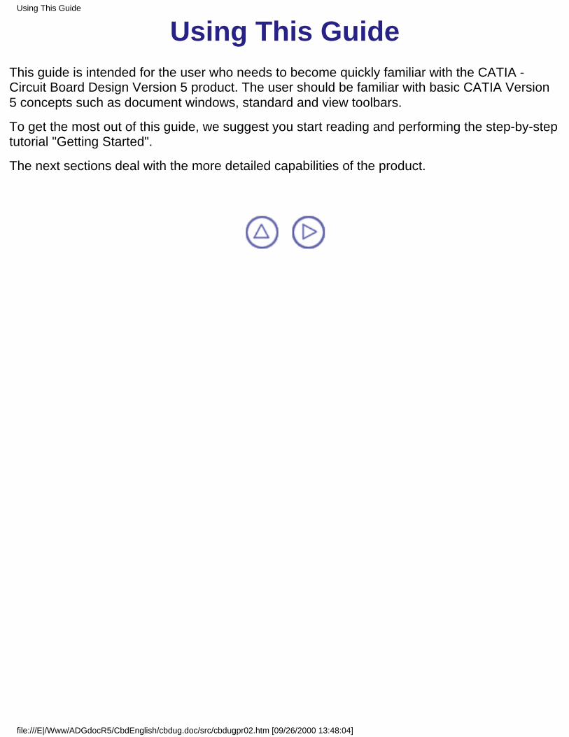
What's New?This table identifies what new or improved capabilities have been documented in the Version 5Release 5 of CATIA - Circuit Board Design User's Guide.
New: Import and Export using IDF 3.0New: Panel ObjectNew: Annotations ManagementNew: Import in Context with ReconciliationNew: Offset ManagementEnhanced: Component Properties
What's New?
file:///E|/Www/ADGdocR5/CbdEnglish/cbdug.doc/src/cbdugwn.htm [09/26/2000 13:48:14]

Getting StartedBefore getting into the detailed instructions for using CATIA - Circuit Board DesignVersion 5, the following tutorial provides a step-by-step scenario demonstrating howto use key functionalities.
Before starting this scenario, you should be familiar with the basic commandscommon to all workbenches. These are described in the CATIA - InfrastructureUser's Guide.The main tasks proposed in this section are:
Accessing the WorkbenchCreating a BoardPocket and HolesConstraint AreaExporting DataImporting Data
All together, these tasks should take about 15 minutes to complete.
Getting Started
file:///E|/Www/ADGdocR5/CbdEnglish/cbdug.doc/src/cbduggs01.htm [09/26/2000 13:48:21]

Accessing the Circuit Board WorkbenchThis task explains how to set up the environment to work with Circuit Board Design.
CATIA V5 is launched. A CATProduct document is displayed.
Make sure the Product1 feature is highlighted before changing workbench.
Choose the Circuit Board Design item from the Start-> Equipments & Systems menu.
1.
The Circuit Board Design workbench is displayed and ready to use.
Note that a new part Part1 has been automatically added to the specificationtree.It will be used to design the board.You can add the Circuit Board Design workbench to your Favorites, using theTools -> Customize item. For more information, refer to CATIA V5 - InfrastructureUser's Guide.
Accessing the Circuit Board Workbench
file:///E|/Www/ADGdocR5/CbdEnglish/cbdug.doc/src/cbduggs02.htm (1 of 2) [09/26/2000 13:48:23]

Accessing the Circuit Board Workbench
file:///E|/Www/ADGdocR5/CbdEnglish/cbdug.doc/src/cbduggs02.htm (2 of 2) [09/26/2000 13:48:23]

Creating a BoardThis task explains how to create a board then design its geometry.
You are in the Product1 document.The Circuit Board Design workbench is displayed.
Select the Board icon .1.
Select the Sketcher icon .2.
Select the xy plane.
The Sketcher workbench is launched.
3.
Click the Profile icon .4.
Sketch the contour of the Board.To do so:
start the sketch from 1 and go to 4,stop at 4 by double clicking,start again from 5 and go to 10,stop at 10 by double clicking.
Before you click to start then to stop, a bluesymbol must appear to illustrate coincidencebetween the start and end points, to get a closedcontour. Refer to the Sketcher Getting Started.
The profile looks like this:
5.
Quit the Sketcher using the Exit icon :
You are back in the Circuit Board Design workbench.
6.
Click the Pad icon .7.
Creating a Board
file:///E|/Www/ADGdocR5/CbdEnglish/cbdug.doc/src/cbduggs00.htm (1 of 2) [09/26/2000 13:48:30]

The Pad Definition dialog box appears.
Enter 2mm in the Length field.8.
Click OK.The pad turns green, this means the board has been created.The board has been created from the active part: Part1(BOARD).
CATIA recognizes the first pad created as the board.
9.
For more information about the Sketcher, refer to the CATIA V5 - Sketcher User's Guide.
Creating a Board
file:///E|/Www/ADGdocR5/CbdEnglish/cbdug.doc/src/cbduggs00.htm (2 of 2) [09/26/2000 13:48:30]

Creating a Pocket and HolesThis task shows how to create a pocket and two holes.
Sketch the contour of the pocket.
To do so:
click the Sketcher icon .
select the board to define the working planeb.
click the Profile icon and draw the contourc.
then click the Exit Sketcher icon to return to the 3D world.d.
1.
Click the Pocket icon .The Pocket Definition dialog box is displayed and CATIA previews a pocket with defaultparameters.
2.
Set the Up to last option to define the pocket limit.3.
Pocket and Holes
file:///E|/Www/ADGdocR5/CbdEnglish/cbdug.doc/src/cbduggs03.htm (1 of 3) [09/26/2000 13:48:35]

This means that the application will extend thepocket to the last possible face, that is the padbottom.
Click OK.4.
Click the Hole icon .5.
Select the board to define the working plane.The Hole Definition dialog box appears.CATIA previews the hole to be created with default parameters.
6.
Enter 4mm for the diameter and click OK.The hole is created.
7.
Repeat the steps 5, 6 and 7 for the second hole.The pocket and holes are added to the specification tree.
8.
Pocket and Holes
file:///E|/Www/ADGdocR5/CbdEnglish/cbdug.doc/src/cbduggs03.htm (2 of 3) [09/26/2000 13:48:35]

Pocket and Holes
file:///E|/Www/ADGdocR5/CbdEnglish/cbdug.doc/src/cbduggs03.htm (3 of 3) [09/26/2000 13:48:35]

Creating a Constraint AreaThis task shows you how to create constraint areas.The constraint areas belong to the board part in separate bodies.
Choose the Insert -> Body menu item.1.
Double-click to activate the newly created body.2.
Select the Sketcher icon .3.
Select the board to define the working plane.4.
Click the Profile icon and draw the following contour:5.
Click the Exit Sketcher icon to return to the 3D world.6.
Click the Pad icon .The Pad Definition dialog box appears.
7.
Enter 1mm for the Length.8.
Click OK to validate.9.
Select the Constraint Area icon .10.
Constraint Area
file:///E|/Www/ADGdocR5/CbdEnglish/cbdug.doc/src/cbduggs04.htm (1 of 4) [09/26/2000 13:48:42]

The Constraint Areas dialog box opens.
Choose the PLACE_OUTLINE type and click OK.The PLACE_OUTLINE area is displayed in transparency.
11.
Repeat steps 1 to 10 to create another constraint area on the other face of theboard according to the following contour:
12.
Constraint Area
file:///E|/Www/ADGdocR5/CbdEnglish/cbdug.doc/src/cbduggs04.htm (2 of 4) [09/26/2000 13:48:42]

Select the Constraint Area icon .The Constraint Areas dialog box opens.
13.
Choose the PLACE_KEEPOUT type and click OK.The PLACE_KEEPOUT area is displayed in transparency.
14.
The pads are more than simple pads: they have technological properties.
An alternative: the steps 10 and 11 can take place before step 3.
Constraint Area
file:///E|/Www/ADGdocR5/CbdEnglish/cbdug.doc/src/cbduggs04.htm (3 of 4) [09/26/2000 13:48:42]

Constraint Area
file:///E|/Www/ADGdocR5/CbdEnglish/cbdug.doc/src/cbduggs04.htm (4 of 4) [09/26/2000 13:48:42]

Exporting Data (as IDF)This task shows how to export data to an IDF file.
Click the Export icon .The Export dialog box opens.
1.
Enter DemoExport in the File name field.2.
Press Save.An Information message is displayed:
3.
Click OK to close the information window.4.
Exporting Data
file:///E|/Www/ADGdocR5/CbdEnglish/cbdug.doc/src/cbduggs05.htm [09/26/2000 13:48:47]

Importing the IDF FileThis task shows how to import the IDF data previously saved to a new document.You can also import IDF data from an ECAD system.
Select File -> Open in the menu bar.The File Selection dialogbox opens.
1.
Select .idf in the Files of type field.2.
Select the DemoExport.idf file.3.
Press Open.The Circuit Board DesignImport window pops up.
The DemoExport.idf file is already selected.
4.
Press OK.The Status bar indicates the progression.The result should look like this:
5.
Importing Data
file:///E|/Www/ADGdocR5/CbdEnglish/cbdug.doc/src/cbduggs06.htm (1 of 2) [09/26/2000 13:48:51]

Importing Data
file:///E|/Www/ADGdocR5/CbdEnglish/cbdug.doc/src/cbduggs06.htm (2 of 2) [09/26/2000 13:48:51]

Basic TasksThe Basic Tasks section explains and illustrates how to create various kinds of features.The table below lists the information you will find.
Accessing the Circuit Board WorkbenchCreating a Panel (IDF 3.0)
Creating a BoardCreating Constraint AreasCreating Pocket and Holes
Patterning HolesManaging Components
Exporting DataImporting
Working with CatalogsWorkbench Integration
Basic Tasks
file:///E|/Www/ADGdocR5/CbdEnglish/cbdug.doc/src/cbdugbt0000.htm [09/26/2000 13:48:59]

Accessing the Circuit Board WorkbenchThis task explains how to set up the environment.
Choose the Circuit Board Design item from the Start-> Equipments & Systems menu.
1.
The Circuit Board Design workbench is displayed and ready to use.
You can add the Circuit Board Design workbench to your Favorites, using the Tools ->Customize item. For more information, refer to CATIA V5 - Infrastructure User's Guide.
Accessing the Circuit Board Workbench
file:///E|/Www/ADGdocR5/CbdEnglish/cbdug.doc/src/cbdugbt1000.htm [09/26/2000 13:54:08]

PanelCreate from scratch: Sketch a profile to create a pad to be the panel.Using an IDF file: Import the data from an IDF 3.0 file.
Creating a Panel (IDF 3.0)
file:///E|/Www/ADGdocR5/CbdEnglish/cbdug.doc/src/cbdugbt1100.htm [09/26/2000 13:54:11]

Creating a PanelThis task explains how to create a panel and design its geometry.A panel is an optional file used for manufacturing information exchange (IDF 3.0only).
Open a new CATPart document.
Select the Panel icon .It creates the panel behavior.
1.
Select the Sketcher icon .2.
Select the xy plane.
The Sketcher workbench is launched.
3.
Click the Profile icon .4.
Sketch the contour of the panel.The profile looks like this:
5.
Quit the Sketcher using the Exit icon :
You are back in the Circuit Board Design workbench.
6.
From Scratch
file:///E|/Www/ADGdocR5/CbdEnglish/cbdug.doc/src/cbdugbt1101.htm (1 of 3) [09/26/2000 13:54:13]

Click the Pad icon .The Pad Definition dialog box appears.
7.
Enter 2mm in the Length field.8.
Click OK.The pad turns "sea green", this means the panel representation has beencreated.The panel has been created from the active part: Part1.
9.
By default, CATIA recognizes the first pad created as a panel.For more information about the Sketcher, refer to the CATIA V5 - Sketcher User'sGuide.
From Scratch
file:///E|/Www/ADGdocR5/CbdEnglish/cbdug.doc/src/cbdugbt1101.htm (2 of 3) [09/26/2000 13:54:13]

From Scratch
file:///E|/Www/ADGdocR5/CbdEnglish/cbdug.doc/src/cbdugbt1101.htm (3 of 3) [09/26/2000 13:54:13]

Creating a Panel Using an IDF FileThis task explains how to create a panel by importing an IDF (3.0) file.A panel is an optional file used for manufacturing information exchange (IDF 3.0 only).
You are in Circuit Board Design workbench..
Select the File -> Open menu.The File Selection dialog box opens.
1.
Select the samplepanel.idf file.The Circuit Board Design Import dialog box opens:
Note that:an IDF file only contains the description of one panel or one board.when the panel import file also refers to board, the board part number is indicated in the file.The Edit Links icon is enabled to let you find the board import files.
2.
Click the Edit Links icon .The Circuit Board Design Links dialog box opens:
3.
Navigate using the button to locate the board import files:Sampleboardfile.idfSampleboard.lib
When done the respective lights turn green.
4.
Click Apply to update the Links window.5.
Importing (IDF 3.0)
file:///E|/Www/ADGdocR5/CbdEnglish/cbdug.doc/src/cbdugbt1102.htm (1 of 3) [09/26/2000 13:54:19]

Close the Links window. You come back to the Circuit Board Design Import dialog box.6.
Navigate using the button to locate the panel library file: Samplepanel.lib.When done the Library light turns green.The dialog box looks like this:
7.
Click the OK to validate.The status bar indicates the import progression.The result looks like this:
8.
You can also use catalog files for both the panel and board imports, if needed.
Importing (IDF 3.0)
file:///E|/Www/ADGdocR5/CbdEnglish/cbdug.doc/src/cbdugbt1102.htm (2 of 3) [09/26/2000 13:54:19]

Importing (IDF 3.0)
file:///E|/Www/ADGdocR5/CbdEnglish/cbdug.doc/src/cbdugbt1102.htm (3 of 3) [09/26/2000 13:54:19]

BoardCreate from scratch: Sketch a profile to create a pad to be the board.Create from an existing part: In a CATPart document, select the pad to become theboard.Recognize in Assembly context: In a CATProduct document, select a previouslycreated pad, possibly with holes and pockets. They all get technological properties.
Creating a Board
file:///E|/Www/ADGdocR5/CbdEnglish/cbdug.doc/src/cbdugbt0100.htm [09/26/2000 13:54:28]

Create a Board From ScratchThis task explains how to create a board and design its geometry.
The Circuit Board Design functions are available when you are in the Part Designenvironment.Several functions are integrated from the Part Design workbench.
Choose the Circuit Board Design workbench. A new CATPart document opens.
Select the Board icon .It creates the board behavior.
1.
Select the Sketcher icon .2.
Select the xy plane.
The Sketcher workbench is launched.
3.
Click the Profile icon .4.
Sketch the contour of the Board.The profile looks like this:
5.
Quit the Sketcher using the Exit icon :
You are back in the Circuit Board Design workbench.
6.
Click the Pad icon .The Pad Definition dialog box appears.
7.
From Scratch
file:///E|/Www/ADGdocR5/CbdEnglish/cbdug.doc/src/cbdugbt0102.htm (1 of 2) [09/26/2000 13:54:30]

Enter 2mm in the Length field.8.
Click OK.The pad turns green, this means the board representation has been created.The board has been created from the active part: Part1.
9.
By default, CATIA recognizes the first pad created as the Board.
For more information about the Sketcher, refer to the CATIA V5 - Sketcher User's Guide.
From Scratch
file:///E|/Www/ADGdocR5/CbdEnglish/cbdug.doc/src/cbdugbt0102.htm (2 of 2) [09/26/2000 13:54:30]

From a Previously Created PartThis task shows how to create a board from an existing part.
Open the Scenario1.CATProduct document.It contains a part with two pads.
Click the Board icon .The PartBody contains two pads, so you have to select the pad which will represent the board.
1.
Select Pad.1.CATIA recognizes the board and displays it in green.You can add holes, pockets and constraint areas, as well as technological properties
2.
From Previously Created Part
file:///E|/Www/ADGdocR5/CbdEnglish/cbdug.doc/src/cbdugbt0101.htm (1 of 2) [09/26/2000 13:54:35]

From Previously Created Part
file:///E|/Www/ADGdocR5/CbdEnglish/cbdug.doc/src/cbdugbt0101.htm (2 of 2) [09/26/2000 13:54:35]

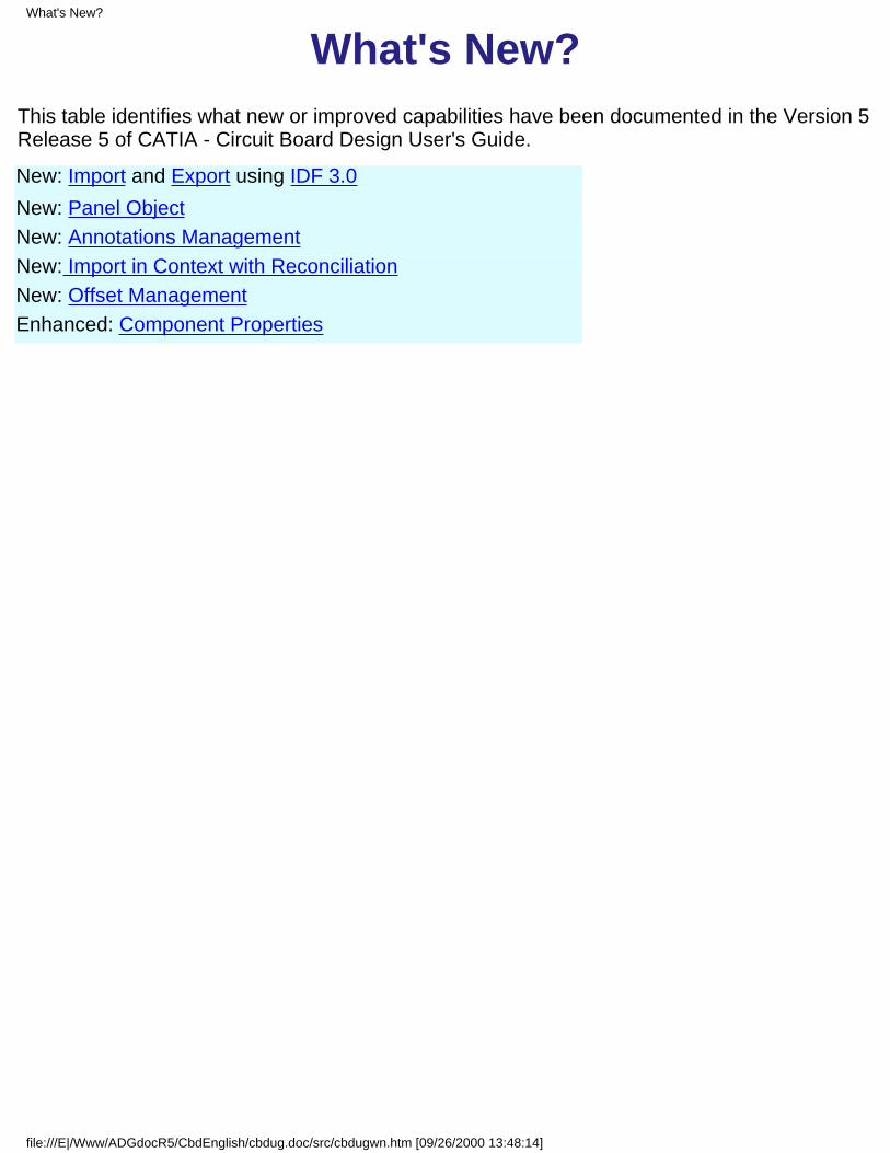
Automatic Recognitionin Assembly Context
This task illustrates how Circuit Board features are automatically recognized.
Open the Scenario2.CATProduct document.It contains a part with a pad, holes and a pocket.
Click the Board icon .Since there is only one pad, it is recognized to be the board representation.The objects (board and holes) have automatically acquired technological properties:
1.
Select the Export icon .A board is recognized, all the related features are taken into account and exported to the IDFfile.
2.
Open the .idf file as a text file. It looks like this:3.
Automatic Recognition
file:///E|/Www/ADGdocR5/CbdEnglish/cbdug.doc/src/cbdugbt0104.htm (1 of 2) [09/26/2000 13:54:43]
Automatic Recognition
file:///E|/Www/ADGdocR5/CbdEnglish/cbdug.doc/src/cbdugbt0104.htm (2 of 2) [09/26/2000 13:54:43]

Constraint AreaSketch a profile to create a pad and assign it to the Constraint Area.Add technological Properties to the constraint area.Use the Settings to change the Constraint Area default colors.
Constraint Areas
file:///E|/Www/ADGdocR5/CbdEnglish/cbdug.doc/src/cbdugbt0600.htm [09/26/2000 13:54:49]

Creating a Constraint AreaThis task shows you how to create a constraint area.
A constraint area is a space reservation used for different purposes such asallowing/forbidding the routing or placing of components etc.Each constraint area belongs to a separate body under the Board PartBody.
Open a CATProduct document, containing a board.
Choose the Insert -> Body menu item.1.
Select the Sketcher icon .2.
Select the board to define the working plane.3.
Click the Profile icon and draw the contour of the constraint area.4.
Click the Exit Sketcher icon to return to the 3D world.5.
Click the Pad icon .The Pad Definition dialog box appears.
6.
Enter 5mm in the Length field.7.
Creating Constraint Areas
file:///E|/Www/ADGdocR5/CbdEnglish/cbdug.doc/src/cbdugbt0601.htm (1 of 3) [09/26/2000 13:54:51]

Select the Constraint Area icon .The Constraint Areas dialogbox opens.
The constraint area types are:Route outline: an area where routing electrical connections is allowedPlace outline: an area where component placing is allowedOther outline: other area type defined by an outline, cutouts and a
thicknessVia keepout: an area where via placing is forbiddenPlace keepout: a mechanical space reservation where the component
height is limitedPlace region: an area where placing is limited to component of
certain typesRoute keepout: an area where routing electrical connections is
forbidden
8.
Choose the Place_KEEPOUT type and click OK.9.
The PLACE_KEEPOUT area is displayed in transparency.
Creating Constraint Areas
file:///E|/Www/ADGdocR5/CbdEnglish/cbdug.doc/src/cbdugbt0601.htm (2 of 3) [09/26/2000 13:54:51]

The pad is more than a simple pad: it has technological properties.
Creating Constraint Areas
file:///E|/Www/ADGdocR5/CbdEnglish/cbdug.doc/src/cbdugbt0601.htm (3 of 3) [09/26/2000 13:54:51]
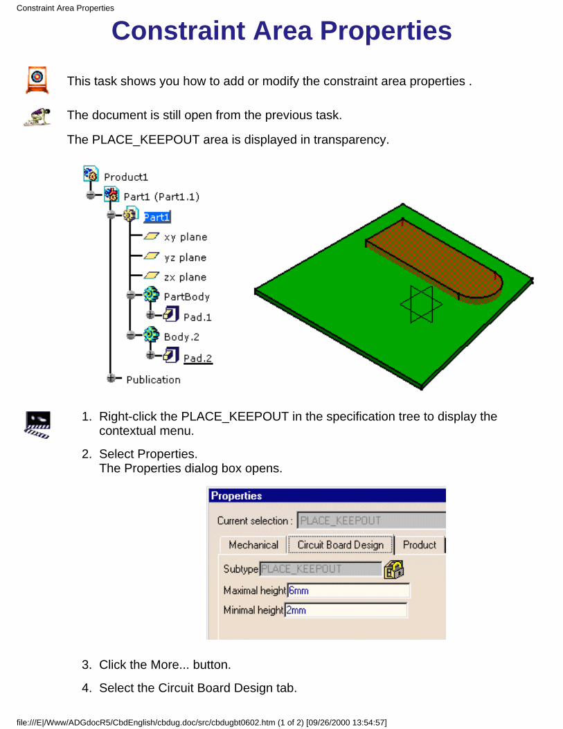
Constraint Area PropertiesThis task shows you how to add or modify the constraint area properties .
The document is still open from the previous task.
The PLACE_KEEPOUT area is displayed in transparency.
Right-click the PLACE_KEEPOUT in the specification tree to display thecontextual menu.
1.
Select Properties.The Properties dialog box opens.
2.
Click the More... button.3.
Select the Circuit Board Design tab.4.
Constraint Area Properties
file:///E|/Www/ADGdocR5/CbdEnglish/cbdug.doc/src/cbdugbt0602.htm (1 of 2) [09/26/2000 13:54:57]

Enter 6mm in the Maximal height field and 2mm in the Minimal height field.5.
Then click OK.The pad is updated: the maximal and minimal height are linked to the pad limits.It represents the overall dimensions of the constraint area.
6.
Constraint Area Properties
file:///E|/Www/ADGdocR5/CbdEnglish/cbdug.doc/src/cbdugbt0602.htm (2 of 2) [09/26/2000 13:54:57]

Changing the Constraint AreasColor Settings
This task shows you how to change the user settings. These are permanent settings.
Select the Tools -> Options menu.The Options dialog box opens.
1.
Click Equipments & Systems in the left-hand box.2.
Click the Circuit Board Design workbench:The Circuit Board tab is displayed.
You can set the color of your choice to the different areas.If you check the Update documents in session box, your change will beapplied to the current document.You can also specify the default catalog.You can set a default height for the component.
3.
Click OK to validate.4.
Color Settings
file:///E|/Www/ADGdocR5/CbdEnglish/cbdug.doc/src/cbdugbt0603.htm (1 of 2) [09/26/2000 13:55:02]

Color Settings
file:///E|/Www/ADGdocR5/CbdEnglish/cbdug.doc/src/cbdugbt0603.htm (2 of 2) [09/26/2000 13:55:02]

Creating a Pocket and HolesThis task shows how to create a pocket and holes, with technological properties.
Open a CATProduct document, containing a board.
Sketch the contour of the pocket.
To do so:
click the Sketcher icon .
select the board to define the working planeb.
click the Profile icon and draw the contour around the motorc.
then click the Exit Sketcher icon to return to the 3D world.d.
1.
Creating Pocket and Holes
file:///E|/Www/ADGdocR5/CbdEnglish/cbdug.doc/src/cbdugbt0800.htm (1 of 4) [09/26/2000 13:55:09]

Click the Pocket icon .
The Pocket Definition dialog box is displayed and CATIA previews a pocketwith default parameters.
2.
Set the Up to last option to define the pocket limit.This means that the application willextend the pocket to the last possibleface, that is the pad bottom.
3.
Click OK.4.
Before creating the Hole, right-click the board PartBody and select Define inWork Object.
5.
Click the Hole icon .6.
Select the board to define the working plane.The Hole Definition dialog box appears.CATIA previews the hole to be created with default parameters.
7.
Enter 4mm for the diameter and click OK.The hole is created.
8.
Repeat the steps 5, 6 and 7 for the second hole. The pocket and holes areadded to the specification tree.
9.
Creating Pocket and Holes
file:///E|/Www/ADGdocR5/CbdEnglish/cbdug.doc/src/cbdugbt0800.htm (2 of 4) [09/26/2000 13:55:09]

Right-click the Hole.1 in the specification tree to display the contextual menu.10.
Select Properties.The Properties dialog box opens.
11.
Click the More... button.12.
Select the Circuit Board tab.13.
Switch the Subtype to NPTH (non conductive) and click OK.The hole is more than a simple hole: it has a technological property.
14.
Repeat the steps 9 to 13 for the second hole.These holes are used for mounting purposes.
15.
Creating Pocket and Holes
file:///E|/Www/ADGdocR5/CbdEnglish/cbdug.doc/src/cbdugbt0800.htm (3 of 4) [09/26/2000 13:55:09]

Creating Pocket and Holes
file:///E|/Www/ADGdocR5/CbdEnglish/cbdug.doc/src/cbdugbt0800.htm (4 of 4) [09/26/2000 13:55:09]

PatternsCreate a hole then define a patternPattern Usage During Import: if a component uses a pattern for mounting purpose,the pattern is recognized during import.Move/Delete Component Using a Pattern: move or delete the holes associated.Delete Pattern: delete the holes associated.
Patterns
file:///E|/Www/ADGdocR5/CbdEnglish/cbdug.doc/src/cbdugbt0700.htm [09/26/2000 13:55:17]

Pattern Designfor Hole or Cutout
This task shows you how to create a pattern for holes or cutouts.Patterns are often used for mounting purpose.
Open a new CATProduct document and create a board.
Select the Hole icon to create the hole to be patterned.1.
Select the Rectangular Pattern icon .2.
Select the hole to pattern.The Rectangular Pattern Definition dialog box opens.Enter the following values for thefirst direction:
Instances: 6Spacing: 10mmReference Direction: selectthe bottom edge (Edge.1)Reverse the direction.
For the second direction:Instances: 2Spacing: 20mmReference Direction: selectthe left edge (Edge.2)
3.
Create Pattern
file:///E|/Www/ADGdocR5/CbdEnglish/cbdug.doc/src/cbdugbt0701.htm (1 of 3) [09/26/2000 13:55:19]

Click OK to validate.The pattern is added to the specification tree and the result looks like this:
4.
For more information about patterns, refer to CATIA - Part Design.
Create Pattern
file:///E|/Www/ADGdocR5/CbdEnglish/cbdug.doc/src/cbdugbt0701.htm (2 of 3) [09/26/2000 13:55:19]

Create Pattern
file:///E|/Www/ADGdocR5/CbdEnglish/cbdug.doc/src/cbdugbt0701.htm (3 of 3) [09/26/2000 13:55:19]

Pattern Usage During ImportThis task shows you that the rectangular pattern used for mounting a component, is recognizedduring import.Before starting, set the Tools -> Options -> Part -> General as shown below:
Open the Pattern.idf document from the samples directory.The Circuit Board Design Import dialog box opens.
1.
Click to activate the Catalog light.2.
Browse to select the Pattern.catalog.The Catalog light becomes green.
3.
Click OK to validate.The import result looks like this:
4.
Pattern Usage
file:///E|/Www/ADGdocR5/CbdEnglish/cbdug.doc/src/cbdugbt0703.htm (1 of 2) [09/26/2000 13:55:24]
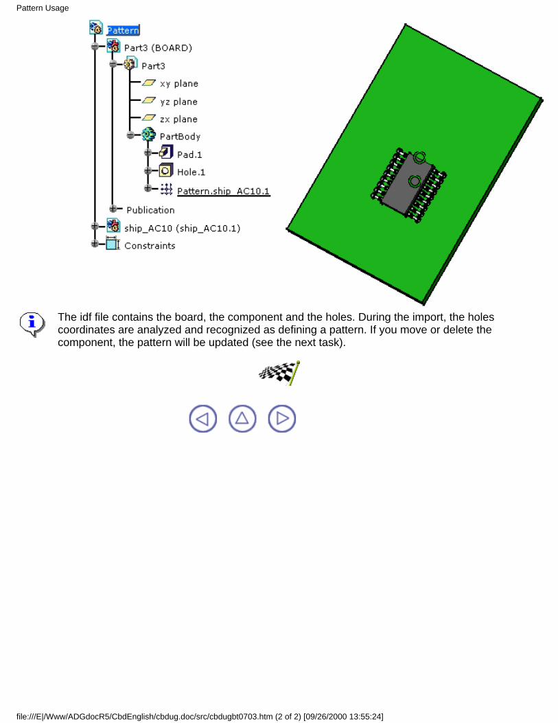
The idf file contains the board, the component and the holes. During the import, the holescoordinates are analyzed and recognized as defining a pattern. If you move or delete thecomponent, the pattern will be updated (see the next task).
Pattern Usage
file:///E|/Www/ADGdocR5/CbdEnglish/cbdug.doc/src/cbdugbt0703.htm (2 of 2) [09/26/2000 13:55:24]

Move PatternThis task shows you how the pattern is modified when a component using thispattern is moved or deleted.
The document is still open from the previous task.
Switch to the Assembly Design workbench.1.
Select the Manipulation icon .The Manipulation Parameters dialog box opens.
2.
Select the Drag along any plane icon.3.
Move the component to the top left corner.4.
Move Pattern
file:///E|/Www/ADGdocR5/CbdEnglish/cbdug.doc/src/cbdugbt0704.htm (1 of 3) [09/26/2000 13:55:30]

When you release the mouse button, the board turns red: it needs to beupdated.
Click the Update icon .The pattern is shifted to the component location.
5.
Move Pattern
file:///E|/Www/ADGdocR5/CbdEnglish/cbdug.doc/src/cbdugbt0704.htm (2 of 3) [09/26/2000 13:55:30]

Move Pattern
file:///E|/Www/ADGdocR5/CbdEnglish/cbdug.doc/src/cbdugbt0704.htm (3 of 3) [09/26/2000 13:55:30]

Delete PatternThis task shows you how to delete a pattern
The document is still open from the previous task.
Select the pattern feature in the specification tree.1.
Press the Delete key or right-click to use the contextual menu: Delete.
The Delete dialog boxopens.
2.
Check the Delete exclusive parents box if you also want to remove the firsthole.
3.
Click OK to validate.The Confirm Deletion dialog box pops up.
4.
Delete Pattern
file:///E|/Www/ADGdocR5/CbdEnglish/cbdug.doc/src/cbdugbt0702.htm (1 of 2) [09/26/2000 13:55:36]

Press Yes to confirm.The pattern has been removed.
5.
Delete Pattern
file:///E|/Www/ADGdocR5/CbdEnglish/cbdug.doc/src/cbdugbt0702.htm (2 of 2) [09/26/2000 13:55:36]

ComponentsCreate: Click this icon, enter a package number then select the pad to become thecomponent.Properties: Right-click the component to browse its technological properties.Constraints: Double-click a constraint to edit the component status.
Managing Components
file:///E|/Www/ADGdocR5/CbdEnglish/cbdug.doc/src/cbdugbt0300.htm [09/26/2000 13:55:43]

Creating a ComponentThis task explains how to create and manage components.
Open the Component.CATProduct document.The window looks like this:
Select the Component icon .The New Component dialog box opens.
1.
Enter comp1 in the Package number field.2.
Click OK to validate.3.
Select Pad.1 in the specification tree. It is the geometrical representation of the new component.
4.
The component is created.
Component Creation
file:///E|/Www/ADGdocR5/CbdEnglish/cbdug.doc/src/cbdugbt0301.htm (1 of 2) [09/26/2000 13:55:46]

Component Creation
file:///E|/Www/ADGdocR5/CbdEnglish/cbdug.doc/src/cbdugbt0301.htm (2 of 2) [09/26/2000 13:55:46]

Component PropertiesThis task shows how to browse the technological properties of a component.
Select a component.1.
Using the right mouse button, open the Properties dialog box.2.
Click the More... button then select the Circuit Board Design tab.In this example, the component is located on the Top face and its Status is Unplaced.
3.
You can change the Component Status to Placed.A placement constraint is created. Using Assembly capabilities, you can edit this constraint.
You can change the offset value.The offset value is taken into account when you export the data in IDF 3.0.
You can still move the component to the desired location on the surface of the board.
4.
You can change the Status to Fixed.The FixTogether Constraint is created between the board and the component.
5.
Component Properties
file:///E|/Www/ADGdocR5/CbdEnglish/cbdug.doc/src/cbdugbt0302.htm (1 of 2) [09/26/2000 13:55:53]

Other properties come up with IDF 3.0 file support such as:Optional Attributes:
CapacitanceResistanceToleranceetc.
as well as user defined attributes (optional).They can be valuated in this dialog box.
6.
Click OK to validate.7.
Component Properties
file:///E|/Www/ADGdocR5/CbdEnglish/cbdug.doc/src/cbdugbt0302.htm (2 of 2) [09/26/2000 13:55:53]

Components and ConstraintsThis task explains how to manage components given the component constraint type.
Open the Scenario3.idf file and the corresponding Scenario3.lib file from the samples folder.An Assembly Product document is generated.
If the configuration you are using provides access to the Assembly Design workbench,geometrical constraints are created between the board and the components, and aredisplayed.Within the assembly, the board need to be anchored.
Double-click the power-jack constraint shown here in red.
The Constraint Edition dialog box opens.The constraint type is either Surface Contact(placed component) or Fix Together (fixedcomponent).
1.
Components and Constraints
file:///E|/Www/ADGdocR5/CbdEnglish/cbdug.doc/src/cbdugbt0303.htm (1 of 2) [09/26/2000 13:59:15]

The Assembly constraints (geometrical constraints) linking the components to the boarddepend on the component status.
Component Status Assembly ConstraintUnplaced No Constraint
Placed Plane to Plane ConstraintFixed Fixity Constraint
This information is transmitted through the import file (.idf), the component capability tochange location is then driven by the constraint.
Under certain circumstances, a component status can be modified:from unplaced to placed or fixedfrom placed to fixed
but never from fixed to placed or unplaced, nor from placed to unplaced (in order to keep theinformation defined in the ECAD world).
Editing the constraint lets you modify the offset between the component and the board(IDF 3.0):
The IDF 3.0 takes into account the offset which represents a mounting constraint ofthe component onto the board.
2.
The offset is also managed between the board and the panel.
Components and Constraints
file:///E|/Www/ADGdocR5/CbdEnglish/cbdug.doc/src/cbdugbt0303.htm (2 of 2) [09/26/2000 13:59:15]

ExportExporting Data: export a board and components respecting an assembly context
IDF 3.0: sums-up the information added to the export file when using IDF 3.0.
Exporting Data
file:///E|/Www/ADGdocR5/CbdEnglish/cbdug.doc/src/cbdugbt0900.htm [09/26/2000 13:59:21]
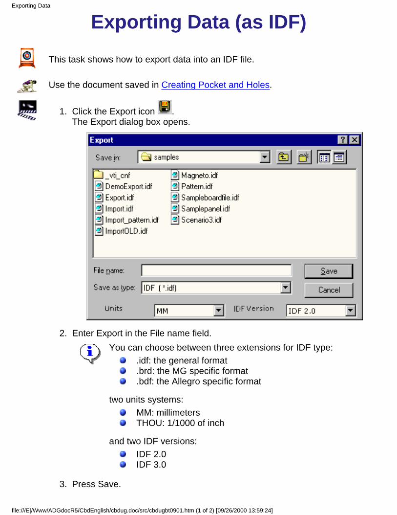
Exporting Data (as IDF)This task shows how to export data into an IDF file.
Use the document saved in Creating Pocket and Holes.
Click the Export icon .The Export dialog box opens.
1.
Enter Export in the File name field.You can choose between three extensions for IDF type:
.idf: the general format
.brd: the MG specific format
.bdf: the Allegro specific format
two units systems:MM: millimetersTHOU: 1/1000 of inch
and two IDF versions:IDF 2.0IDF 3.0
2.
Press Save.3.
Exporting Data
file:///E|/Www/ADGdocR5/CbdEnglish/cbdug.doc/src/cbdugbt0901.htm (1 of 2) [09/26/2000 13:59:24]

An Information message is displayed:
Exporting Data
file:///E|/Www/ADGdocR5/CbdEnglish/cbdug.doc/src/cbdugbt0901.htm (2 of 2) [09/26/2000 13:59:24]

IDF 3.0This file sums-up what information is managed in the export file when using IDF 3.0.
Manufacturing panel information: the panel file is an optional file.The panel file contains the physical description of the manufacturing panel andthe location of the boards and components on that panel. It can be createdinteractively then exported.
1.
Annotations: a new section is added to the file.It contains notes for the design that can be displayed to allow the electrical andmechanical designers to communicate additional information about the designentities. They are not intended for manufacturing purpose. At the moment, theycan only be modified in CATIA then exported.
2.
Offset: the offset field represents the mounting offset for a component onto theboard.It is also available for board mounting offset onto the panel.Placing a component creates a constraint. Editing the constraint allows you tomodify the offset. It will be taken into account in the export file.
3.
Properties: an optional record specifies properties for the component such ascapacitance, resistance, tolerance, power_max, etc. as well as user definedattributes.You can set the values in the Properties dialog box. Your changes will betaken into account in the export file.
4.
IDF 3.0
file:///E|/Www/ADGdocR5/CbdEnglish/cbdug.doc/src/cbdugbt0902.htm [09/26/2000 13:59:33]

ImportOpen an IDF File: import a board and components from an IDF file.
Import in Context: import a board and components respecting an assembly context
IDF 3.0: what is managed during IDF 3.0 importFile Extension Management during importError File Report when the import does not operate properly.
Annotation Management: can be modified in CATIA
Importing
file:///E|/Www/ADGdocR5/CbdEnglish/cbdug.doc/src/cbdugbt0200.htm [09/26/2000 13:59:50]

Opening an IDF FileThis task explains how to import data from an IDF file.
Open the Magneto.idf document from the samples folder.The Circuit Board Design Import window opens.
The .idf file contains the location of the components in the circuit boardassembly.
You can also use a library and/or a catalog to get a better geometry of thecomponents:
the .lib file contains the 2D footprint geometry of the componentsthe .catalog contains the 3D (exact) geometry of the components.
However, none of these two files are mandatory.
You can choose between several alternatives:open a library only: the 3D geometry is extruded from the 2D geometryopen a library and use a catalog: refer to Import with Catalogopen no library and no catalog, the component has no associatedgeometry.
1.
Fill up the library field using the button and select the Magneto.lib file.The light shows, according to a color code:
2.
Open an IDF File
file:///E|/Www/ADGdocR5/CbdEnglish/cbdug.doc/src/cbdugbt0202.htm (1 of 2) [09/26/2000 13:59:53]

if the file is mandatory, the light is redif the file is optional, the light is yellowif your selection is valid, the light turns green.
Click OK to validate.The Status bar indicates the progression.The result looks as follows.
3.
Open an IDF File
file:///E|/Www/ADGdocR5/CbdEnglish/cbdug.doc/src/cbdugbt0202.htm (2 of 2) [09/26/2000 13:59:53]

Importing in ContextThis task explains how to import circuit board elements and place them in context.
Open the Context.CATProduct document.
Enter the Circuit Board Design workbench.A new part is created.
1.
Select the Import in Context icon .2.
Select the plane where you want to place the board and components, that is tosay the CD bottom plane.The Import dialog box is displayed.
3.
Click the button to choose Scenario3.idf file and Scenario3.lib file in therespective fields. It looks like this:
4.
Importing in Context
file:///E|/Www/ADGdocR5/CbdEnglish/cbdug.doc/src/cbdugbt0201.htm (1 of 2) [09/26/2000 13:59:58]
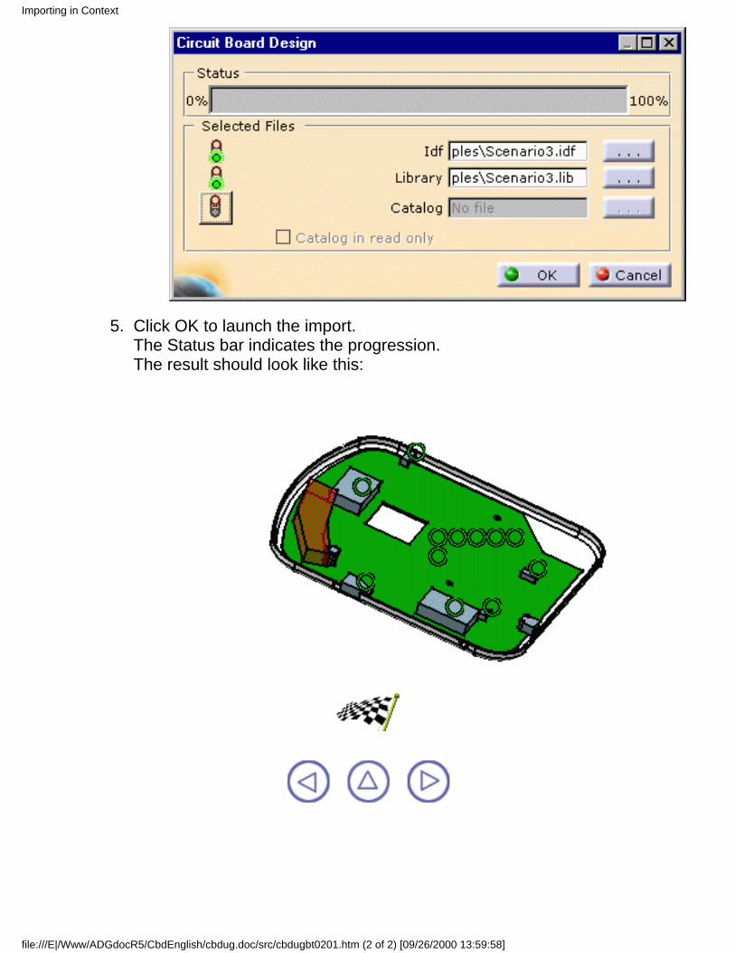
Click OK to launch the import.The Status bar indicates the progression.The result should look like this:
5.
Importing in Context
file:///E|/Www/ADGdocR5/CbdEnglish/cbdug.doc/src/cbdugbt0201.htm (2 of 2) [09/26/2000 13:59:58]

IDF 3.0This file sums-up what information is added to the import file when using IDF 3.0.
Manufacturing panel information: the panel file is an optional file.It has been added (comparatively to IDF 2.0) to allow the exchange ofmanufacturing panel information. The panel file contains the physicaldescription of the manufacturing panel and the location of the boards andcomponents on that panel.
1.
Annotations: a new section is added to the file.It contains notes for the design that can be displayed to allow the electrical andmechanical designers to communicate additional information about the designentities. They are not intended for manufacturing purpose.
2.
Offset: the offset field represents the mounting offset for a component onto theboard.It is also available for board mounting offset onto the panel.
3.
Properties: an optional record specifies properties for the component such ascapacitance, resistance, tolerance, power_max, etc. as well as user definedattributes.
4.
IDF 3.0
file:///E|/Www/ADGdocR5/CbdEnglish/cbdug.doc/src/cbdugbt0205.htm [09/26/2000 14:00:01]

File Extension ManagementDuring Import
This task explains what are the different file extension managed during import.
CATIA - Circuit Board Design works with IDF 2.0 and IDF 3.0 files.According to the application used to generate the file, the extension will bedifferent.
Three extensions are now recognized:.idf: the general format.brd: the Mentor Graphics specificformat.bdf: the Allegro specific format
Two units systems can be read in CATIA:MM: millimetersTHOU: 1/1000 of inch
File extension Imp/Exp.
file:///E|/Www/ADGdocR5/CbdEnglish/cbdug.doc/src/cbdugbt0203.htm [09/26/2000 14:00:04]

Error File ReportingThis task explains what happens when the file import does not operate properly.
The scenario is described in Opening an IDF File.
During the import, if a problem is detected, the import operation continues and theitems generating an error are listed in a report file:
The CATProduct resulting from the import is incomplete, it's to say that somecomponents or areas or parts of the board can be missing or incomplete but theimport itself has finished.
Error File Report
file:///E|/Www/ADGdocR5/CbdEnglish/cbdug.doc/src/cbdugbt0204.htm [09/26/2000 14:00:08]

Annotations ManagementThis task shows how to modify annotations after an import using IDF 3.0.
You have performed the panel import.
Select an Annotation in the specification tree.
The annotation is displayed on the constraint area.
1.
Double-click the annotation.
It shows six parameters. Three of them can be modified in this version:
2.
Annotations (IDF 3.0)
file:///E|/Www/ADGdocR5/CbdEnglish/cbdug.doc/src/cbdugbt0206.htm (1 of 2) [09/26/2000 14:00:14]

the text position (X and Y)the text.
Double-click the Text parameter.The Edit Parameter dialog box opens:
3.
You can change the text of the annotation and click OK.4.
You can do the same for the text position by modifying the X or Y coordinates.5.
These modifications are taken into account when exporting data in an IDF file.
Annotations (IDF 3.0)
file:///E|/Www/ADGdocR5/CbdEnglish/cbdug.doc/src/cbdugbt0206.htm (2 of 2) [09/26/2000 14:00:14]

Using CatalogsExport a Component: create the catalog to store the component.
File -> Open Import: operate with library and/or catalog to get a better components geometry.
Access to the Catalog Editor to insert component.
Working with Catalogs
file:///E|/Www/ADGdocR5/CbdEnglish/cbdug.doc/src/cbdugbt0500.htm [09/26/2000 14:00:20]

Export a ComponentThis task explains how to create a catalog for circuit board components.
Open the Component2.CATProduct document.The component is selected.
Select the Export a Component icon .The catalog dialog box opens.
1.
Enter a name for the catalog.The catalog doesn't exist, you are prompted to create it.
2.
Click Yes.A message informs you that the catalog has been created.
3.
Catalog Creation
file:///E|/Www/ADGdocR5/CbdEnglish/cbdug.doc/src/cbdugbt0501.htm (1 of 2) [09/26/2000 14:00:23]

Click OK to validate.4.
Note that you can store several components at the same time in the catalog.
Catalog Creation
file:///E|/Www/ADGdocR5/CbdEnglish/cbdug.doc/src/cbdugbt0501.htm (2 of 2) [09/26/2000 14:00:23]

Importing Using a CatalogThis task explains how to import data from an IDF file, where the component 3Dgeometry is imported from a catalog.
Open the Import.idf document from the samples directory.The .idf file contains the location of the components in the circuit board assembly.
1.
You can use a library and/or a catalog to get a better geometry of thecomponents:
the .lib file contains the 2D footprint geometry of the components.the .catalog contains the 3D (exact) geometry of the components.
However, none of these files are mandatory.
You can choose between several alternatives:open a library only: the 3D geometry is extruded from the 2Dgeometryopen a library and use an existing catalog:
the component exists in the catalog, its 3D geometry isimported from the catalogthe component does not exist in the catalog, it is extrudedfrom the 2D geometry and stored in the catalog if the catalogis not protected (Catalog in read only box is not checked)
open a library and a new catalog: the 3D geometry is extruded fromthe 2D geometry and stored in the newly created catalogopen no library, but a catalog:
the component exists in the catalog, its 3D geometry isimported from the catalogthe component does not exist in the catalog, it is created withno associated geometry
open no library and no catalog, the component has no associatedgeometry.
The Circuit Board Design dialog box opens.
Import with Catalog
file:///E|/Www/ADGdocR5/CbdEnglish/cbdug.doc/src/cbdugbt0502.htm (1 of 3) [09/26/2000 14:00:30]

The first light is green: the selection is valid.
The second light is red: you need to choose a library.
Browse using the button and select the ImportComps.lib file.The light becomes green.
2.
Click to activate the third light: it becomes red.3.
Browse using the button and select the Import.catalog file.The light becomes green.The check box Catalog in read only preserves your catalog from overwriting.
4.
Click OK to validate.The Status bar indicates the progression. The import is completed.
5.
Note that if you have set a catalog in the Options, it will be proposed by default.
Import with Catalog
file:///E|/Www/ADGdocR5/CbdEnglish/cbdug.doc/src/cbdugbt0502.htm (2 of 3) [09/26/2000 14:00:30]

Import with Catalog
file:///E|/Www/ADGdocR5/CbdEnglish/cbdug.doc/src/cbdugbt0502.htm (3 of 3) [09/26/2000 14:00:30]

CatalogThe integration with the Catalog workbench lets you access to the advanced catalogcapabilities such as the component drag and drop.For more information about Catalogs, refer to CATIA - Infrastructure User's Guide.
Open a catalog and choose the Preview tab.1.
Open a new CATProduct document.2.
Tile the windows horizontally. It looks like this:3.
Select the components you want to copy into the CATProduct.4.
Drag and drop it onto the Product.An alternative is to copy then paste it (Cntl-c then Cntl-v)
5.
The components are copied in the CATProduct document
Catalog à déclarer dans ADELE
file:///E|/Www/ADGdocR5/CbdEnglish/cbdug.doc/src/cbdugbt0503.htm [09/26/2000 14:00:42]

Workbench IntegrationIn Assembly context, move the components on the board, respecting the constraints.
Launch the DMU Space Analysis to perform a clash check.
Workbench Integration
file:///E|/Www/ADGdocR5/CbdEnglish/cbdug.doc/src/cbdugbt0400.htm [09/26/2000 14:00:50]

AssemblyThe integration with the Assembly Design workbench lets you move the componentson the board, provided you are allowed to do so by the related constraints, in thecontext of the full digital product definition.
Refer to the Component Management section for more information.
Assembly
file:///E|/Www/ADGdocR5/CbdEnglish/cbdug.doc/src/cbdugbt0401.htm [09/26/2000 14:00:52]

CATIA-DMU Space AnalysisThe strong integration with CATIA-DMU V5 Space Analysis allows you to completethe analysis of the electronic assembly in the context of the full digital productdefinition.
Open the Scenario3.idf file and the corresponding Scenario3.lib file from the\online\samples\circuitboard directory.An Assembly Product document is generated.Then add the existing component (BOTTOM).
Choose the DMU Space Analysis item from the Start menu.1.
Perform a Check Clash using this icon .2.
CATIA-DMU Space Analysis
file:///E|/Www/ADGdocR5/CbdEnglish/cbdug.doc/src/cbdugbt0402.htm (1 of 3) [09/26/2000 14:00:55]

The Preview window shows the clash:
CATIA-DMU Space Analysis
file:///E|/Www/ADGdocR5/CbdEnglish/cbdug.doc/src/cbdugbt0402.htm (2 of 3) [09/26/2000 14:00:55]

The analysis reveals a clash. You can:either, change the location of the component respecting thegeometrical constraintsor create a mechanical constraint area taking the clash intoaccount; then transmit the information to the ECAD system in orderto integrate it into the placing/routing algorithm.
For more information about DMU Space Analysis capabilities, refer toCATIA-DMU Space Analysis User's Guide.
CATIA-DMU Space Analysis
file:///E|/Www/ADGdocR5/CbdEnglish/cbdug.doc/src/cbdugbt0402.htm (3 of 3) [09/26/2000 14:00:55]

Advanced TasksThe Advanced Tasks section explains and illustrates how to create various kinds of features.The table below lists the information you will find.
Import in Context with ReconciliationJournaling Integration
Advanced Tasks (Not Used)
file:///E|/Www/ADGdocR5/CbdEnglish/cbdug.doc/src/cbdugat0000.htm [09/26/2000 14:01:13]

Import in Context with ReconciliationThis task explains how to create an assembly then replace a document within the assembly withrespect to the constraints using the label publication.
Open a new product document.
Right-click the root product and select Components->New Product :Name it Electrical for example: you will import the board in this one.
1.
Right-click the root product again and select Components->New Product .Name it Mechanical: you will use this one to create the context: the casing.
2.
Right-click the Mechanical product and select Components->Existing Component .The File Selection dialog box opens.
3.
Select the casing.CATPart.At this stage, the document looks like this:
4.
Double-click the Electrical product and select Start->Equipment & Systems-> Circuit boardDesign workbench.
5.
Select the Import in Context icon .You are prompted to select a face as context.
6.
Select the top face of the casing.The Import dialog box opens.
7.
Navigate to select the Reconciliation1.idf file.8.
Navigate to select the default.lib file then click OK.The status bar indicates the import progression.The result looks like this:Note: click the Publication in the specification tree.It shows the association of labels to the geometrical faces of the board: Top and Bottom.
9.
Import in Context with Reconciliation
file:///E|/Www/ADGdocR5/CbdEnglish/cbdug.doc/src/cbdugat0100.htm (1 of 4) [09/26/2000 14:01:16]
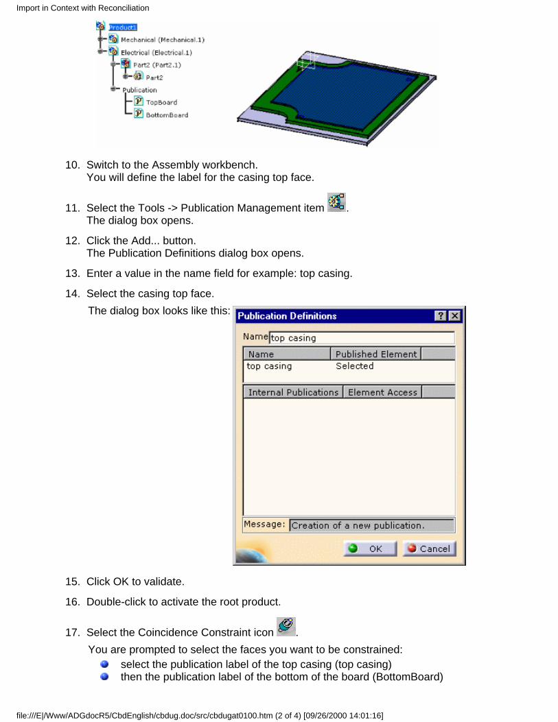
Switch to the Assembly workbench.You will define the label for the casing top face.
10.
Select the Tools -> Publication Management item .The dialog box opens.
11.
Click the Add... button.The Publication Definitions dialog box opens.
12.
Enter a value in the name field for example: top casing.13.
Select the casing top face.The dialog box looks like this:
14.
Click OK to validate.15.
Double-click to activate the root product.16.
Select the Coincidence Constraint icon .You are prompted to select the faces you want to be constrained:
select the publication label of the top casing (top casing)then the publication label of the bottom of the board (BottomBoard)
17.
Import in Context with Reconciliation
file:///E|/Www/ADGdocR5/CbdEnglish/cbdug.doc/src/cbdugat0100.htm (2 of 4) [09/26/2000 14:01:16]

The coincidence constraint is created and the Constraint Properties dialog box opens:
It shows the constraint type, components and status.Click OK to validate.
Right-click the Electrical Product and select Components->Replace Component .The File Selection dialog box opens.
18.
Select the Reconciliation2.idf file.In this file a pocket has been added to the board.The Import dialog box opens to let you choose the default.libThe status bar indicates the progression.The result looks like this:
19.
Double-click the Constraint icon .You can see the Constraint Definition.The coincidence constraint has been maintained although the board has been replaced.
20.
Import in Context with Reconciliation
file:///E|/Www/ADGdocR5/CbdEnglish/cbdug.doc/src/cbdugat0100.htm (3 of 4) [09/26/2000 14:01:16]

Click OK to validate.21.
Import in Context with Reconciliation
file:///E|/Www/ADGdocR5/CbdEnglish/cbdug.doc/src/cbdugat0100.htm (4 of 4) [09/26/2000 14:01:16]

Journaling IntegrationIt is possible to create a board or a constraint area using macros.Refer to the Programming Interface Guide -> PCBBoard and PCBWorkbench.
Journaling Integration
file:///E|/Www/ADGdocR5/CbdEnglish/cbdug.doc/src/cbdugat0200.htm [09/26/2000 14:01:22]

Workbench Description
The CATIA - Circuit Board Design Version 5 application window looks like this:Click the hotspots to display the related documentation.
Menu BarToolbar
Specification Tree
Workbench Description
file:///E|/Www/ADGdocR5/CbdEnglish/cbdug.doc/src/cbdugwd0000.htm [09/26/2000 14:01:32]
Menu BarThe Menu Bar and items which are available in CATIA - Circuit Board Design workbenchare the standard ones. The different commands and tools are described in CATIA -Infrastructure Version 5.
For more information, refer to the CATIA Menu Bar section.
Menu Bar
file:///E|/Www/ADGdocR5/CbdEnglish/cbdug.doc/src/cbdugwd0100.htm [09/26/2000 14:01:35]
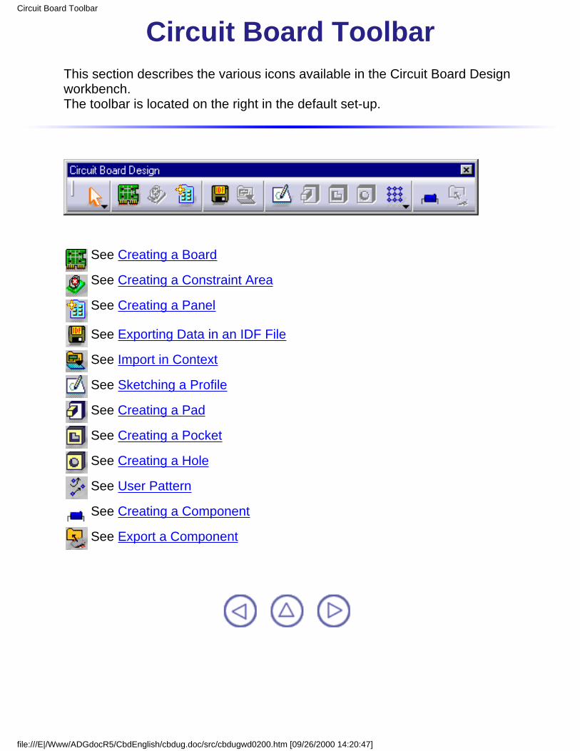
Circuit Board ToolbarThis section describes the various icons available in the Circuit Board Designworkbench.The toolbar is located on the right in the default set-up.
See Creating a Board
See Creating a Constraint Area
See Creating a Panel
See Exporting Data in an IDF File
See Import in Context
See Sketching a Profile
See Creating a Pad
See Creating a Pocket
See Creating a Hole
See User Pattern
See Creating a Component
See Export a Component
Circuit Board Toolbar
file:///E|/Www/ADGdocR5/CbdEnglish/cbdug.doc/src/cbdugwd0200.htm [09/26/2000 14:20:47]

Specification TreeWithin the Circuit Board Design workbench, you can generate a number of features that areidentified in the specification tree by the following icons.
Label associated to the geometrical face of the board
Specification Tree
file:///E|/Www/ADGdocR5/CbdEnglish/cbdug.doc/src/cbdugwd0300.htm [09/26/2000 14:20:55]

GlossaryA
annotations Allow the electrical and mechanical designers to communicate additionalinformation about the design. They are not intended to be used for manufacturingpurpose.
Bboard A pad with technological propertiesBOTTOM The technological property of a board face which makes it the copper plated face
Ccomponent An electronic part defined in the electronic schematic and stored in the ECAD
component librarycomponent status Describes the position of a component on a board:
unplaced: there is no constraint between the component and the boardplaced: there is a surface contact between the component and the boardfixed: there is a fixity constraint between the component and the boardDedicated geometrical constraints are also associated with components anddetermine whether or not you can move them.
constraint area A space reservation used for different purposes such as allowing/forbidding therouting or placing of components etc.Each constraint area belongs to a part, this is to say that you need to create a newpart before creating a constraint area.
cutout A hole or a pocket on a board
Ddrilled hole A hole used to mount a board in its case
EECAD Electrical Computer Aided Design
Ffixed See component status
IIDF Intermediate Data Format
MMCAD Mechanical Computer Aided Design
Glossary
file:///E|/Www/ADGdocR5/CbdEnglish/cbdug.doc/src/cbduggl.htm (1 of 2) [09/26/2000 14:22:16]

NNPTH Non plated: technological property of a hole which is not conductive (mounting
hole)
Ooffset Represents the mounting constraint of a component onto the board. Also available
between the board and the panel.other outline Other area type defined by an outline, cutouts and a thickness
Ppanel Optional file added to IDF 3.0 standard to allow manufacturing information
exchange. It contains the manufacturing panel physical description as well as theboards and components location on the panel.
placed See component statusplace keepout A mechanical space reservation where the component height is limitedplace outline An area where component placing is allowedplace region An area where placing is limited to component of certain typesPTH Plated: technological property of a hole which is conductive
Rroute keepout An area where routing electrical connections is forbiddenroute outline An area where routing electrical connections is allowed
Sstatus See component status
TTOP The technological property of a board face which means it is not the copper plated
face
Uunplaced See component status
Vvia keepout An area where placing via is forbidden
Glossary
file:///E|/Www/ADGdocR5/CbdEnglish/cbdug.doc/src/cbduggl.htm (2 of 2) [09/26/2000 14:22:16]

IndexA
annotations
Bboard
Cconstraint area constraint (geometrical) component status cutout
Ffixed
IIDF IDF (3.0)
NNPTH
Index
file:///E|/Www/ADGdocR5/CbdEnglish/cbdug.doc/src/cbdugix.htm (1 of 2) [09/26/2000 14:22:21]

Ppanel placed place keepout property (technological) PTH
Ooffset
Rrecognition
Uunplaced
Index
file:///E|/Www/ADGdocR5/CbdEnglish/cbdug.doc/src/cbdugix.htm (2 of 2) [09/26/2000 14:22:21]