Circuit Board Design Page 1 Circuit Board Design -...
123
Circuit Board Design Overview Conventions What's New? Getting Started Accessing the Circuit Board Workbench Creating a Board Pocket and Holes Constraint Area Exporting Data Importing Data User Tasks Accessing the Circuit Board Workbench Creating a Panel (IDF 3.0) From Scratch Importing (IDF 3.0) Creating a Board From Scratch From Previously Created Part Automatic Recognition Constraint Areas Creating Constraint Areas Creating a Multi-Domain Constraint Area Constraint Area Properties Color Settings Creating Pocket and Holes Patterns Create Pattern Create Pattern of Pattern Pattern Usage Move Pattern Delete Pattern Managing Components Component Creation Multi-representation Management Component Properties Components and Constraints Exporting Data Exporting Data IDF 3.0 1 Page Circuit Board Design Version 5 Release 13
Transcript of Circuit Board Design Page 1 Circuit Board Design -...

Circuit Board Design
Overview
Conventions
What's New?
Getting Started
Accessing the Circuit Board Workbench Creating a Board Pocket and Holes Constraint Area Exporting Data Importing Data
User Tasks
Accessing the Circuit Board Workbench Creating a Panel (IDF 3.0)
From Scratch Importing (IDF 3.0)
Creating a Board From Scratch From Previously Created Part Automatic Recognition
Constraint Areas Creating Constraint Areas Creating a Multi-Domain Constraint Area Constraint Area Properties Color Settings
Creating Pocket and Holes Patterns
Create Pattern Create Pattern of Pattern Pattern Usage Move Pattern Delete Pattern
Managing Components Component Creation Multi-representation Management Component Properties Components and Constraints
Exporting Data Exporting Data IDF 3.0
1Page Circuit Board Design Version 5 Release 13

Importing Open an IDF File Importing in Context IDF 3.0 File extension Imp/Exp. Error File Report Annotations (IDF 3.0) Filter Holes Drill Holes
Working with Catalogs Catalog Creation Import with Catalog Catalog csv File
Workbench Integration Assembly CATIA-DMU Space Analysis
Import in Context with Reconciliation
Workbench Description
Menu Bar Circuit Board Toolbar Specification Tree
Customizing
Glossary
Index
2Page Circuit Board Design Version 5 Release 13
Overview
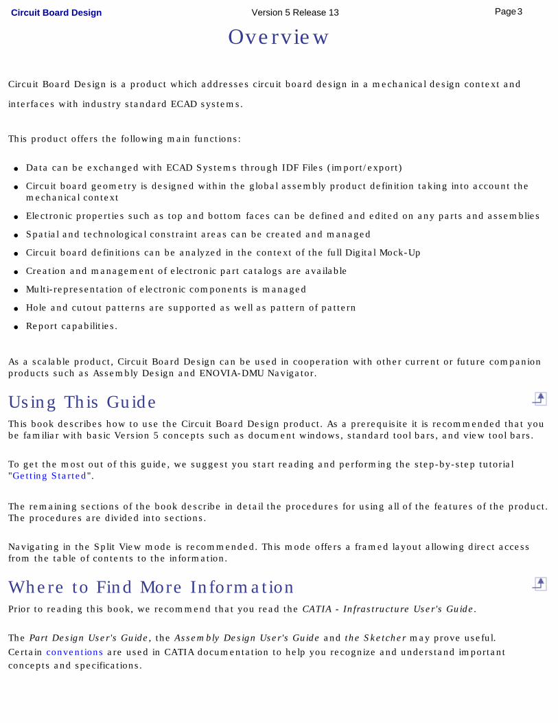
Circuit Board Design is a product which addresses circuit board design in a mechanical design context and
interfaces with industry standard ECAD systems.
This product offers the following main functions:
● Data can be exchanged with ECAD Systems through IDF Files (import/export)
● Circuit board geometry is designed within the global assembly product definition taking into account the mechanical context
● Electronic properties such as top and bottom faces can be defined and edited on any parts and assemblies
● Spatial and technological constraint areas can be created and managed
● Circuit board definitions can be analyzed in the context of the full Digital Mock-Up
● Creation and management of electronic part catalogs are available
● Multi-representation of electronic components is managed
● Hole and cutout patterns are supported as well as pattern of pattern
● Report capabilities.
As a scalable product, Circuit Board Design can be used in cooperation with other current or future companion products such as Assembly Design and ENOVIA-DMU Navigator.
Using This GuideThis book describes how to use the Circuit Board Design product. As a prerequisite it is recommended that you be familiar with basic Version 5 concepts such as document windows, standard tool bars, and view tool bars.
To get the most out of this guide, we suggest you start reading and performing the step-by-step tutorial "Getting Started".
The remaining sections of the book describe in detail the procedures for using all of the features of the product. The procedures are divided into sections.
Navigating in the Split View mode is recommended. This mode offers a framed layout allowing direct access from the table of contents to the information.
Where to Find More InformationPrior to reading this book, we recommend that you read the CATIA - Infrastructure User's Guide.
The Part Design User's Guide, the Assembly Design User's Guide and the Sketcher may prove useful.Certain conventions are used in CATIA documentation to help you recognize and understand important concepts and specifications.
3Page Circuit Board Design Version 5 Release 13
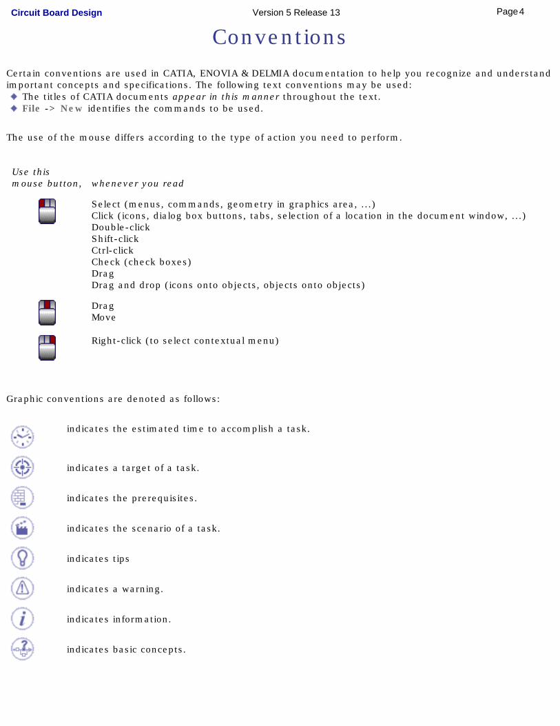
ConventionsCertain conventions are used in CATIA, ENOVIA & DELMIA documentation to help you recognize and understand important concepts and specifications. The following text conventions may be used: The titles of CATIA documents appear in this manner throughout the text. File -> New identifies the commands to be used.
The use of the mouse differs according to the type of action you need to perform.
Use thismouse button, whenever you read
Select (menus, commands, geometry in graphics area, ...)Click (icons, dialog box buttons, tabs, selection of a location in the document window, ...)Double-clickShift-clickCtrl-clickCheck (check boxes)DragDrag and drop (icons onto objects, objects onto objects)
DragMove
Right-click (to select contextual menu)
Graphic conventions are denoted as follows:
indicates the estimated time to accomplish a task.
indicates a target of a task.
indicates the prerequisites.
indicates the scenario of a task.
indicates tips
indicates a warning.
indicates information.
indicates basic concepts.
4Page Circuit Board Design Version 5 Release 13

indicates methodological information.
indicates reference information.
indicates information regarding settings, customization, etc.
indicates the end of a task.
indicates functionalities that are new or enhanced with this Release.Enhancements can also be identified by a blue-colored background in the left-hand margin or on the text itself.
indicates functionalities that are P1-specific.
indicates functionalities that are P2-specific.
indicates functionalities that are P3-specific.
allows you to switch back the full-window viewing mode.
These icons in the table of contents correspond to the entries or mode.
"Site Map".
"Split View" mode.
"What's New".
"Preface".
"Getting Started".
"Basic Tasks".
"User Tasks" or the "Advanced Tasks".
"Workbench Description".
"Customizing".
"Reference".
"Methodology".
5Page Circuit Board Design Version 5 Release 13

"Glossary".
"Index".
6Page Circuit Board Design Version 5 Release 13

What's New?
This table identifies what new or improved capabilities have been documented in the Version 5 Release 13 of Circuit Board Design User's Guide.
No enhancements in this release.
7Page Circuit Board Design Version 5 Release 13

Getting Started
Before getting into the detailed instructions for using Circuit Board Design Version 5, the following tutorial provides a step-by-step scenario demonstrating how to use key functionalities.
Before starting this scenario, you should be familiar with the basic commands common to all workbenches. These are described in the Infrastructure User's Guide.
The main tasks proposed in this section are:
Accessing the Circuit Board WorkbenchCreating a BoardPocket and HolesConstraint AreaExporting DataImporting Data
All together, these tasks should take about 15 minutes to complete.
8Page Circuit Board Design Version 5 Release 13

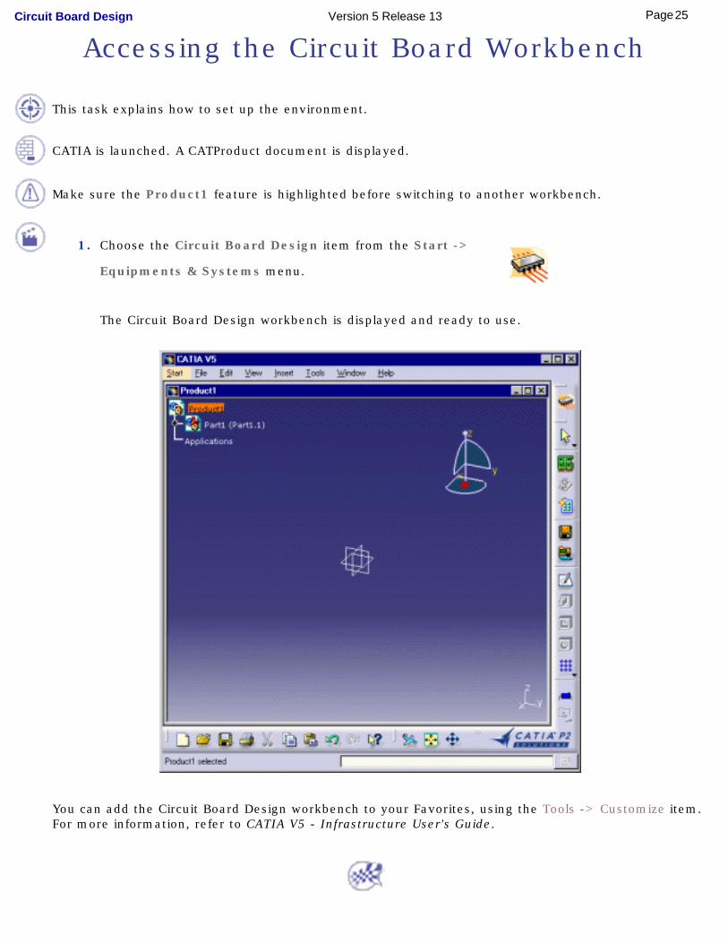
Accessing the Circuit Board Workbench
This task explains how to set up the environment to work with Circuit Board Design.
CATIA is launched. A CATProduct document is displayed.
Make sure the Product1 feature is highlighted before changing workbench.
1. Choose the Circuit Board Design item from the Start ->
Equipments & Systems menu.
The Circuit Board Design workbench is displayed and ready to use.
Note that a new part Part1 has been automatically added to the specification tree.It will be used to design the board.
9Page Circuit Board Design Version 5 Release 13

You can add the Circuit Board Design workbench to your Favorites, using the Tools -> Customize item. For more information, refer to CATIA V5 - Infrastructure User's Guide.
10Page Circuit Board Design Version 5 Release 13

Creating a Board
This task explains how to create a board and design its geometry.
You are working with the Product1 document.The Circuit Board Design workbench is displayed.
1. Select the Create Board button .
2. Select the Sketcher button .
3. Select the xy plane.
The Sketcher workbench is launched.
4. Click the Profile button .
5. Sketch the contour of the Board.
To do so: ❍ start the sketch from 1 and go to 4,
❍ stop at 4 by double clicking,
❍ start again from 5 and go to 10,
❍ stop at 10 by double clicking.
Before you click to start and stop, a blue symbol must appear to illustrate coincidence between the start and end points, to get a closed contour. Refer to the Sketcher Getting Started.
The profile looks like this:
11Page Circuit Board Design Version 5 Release 13
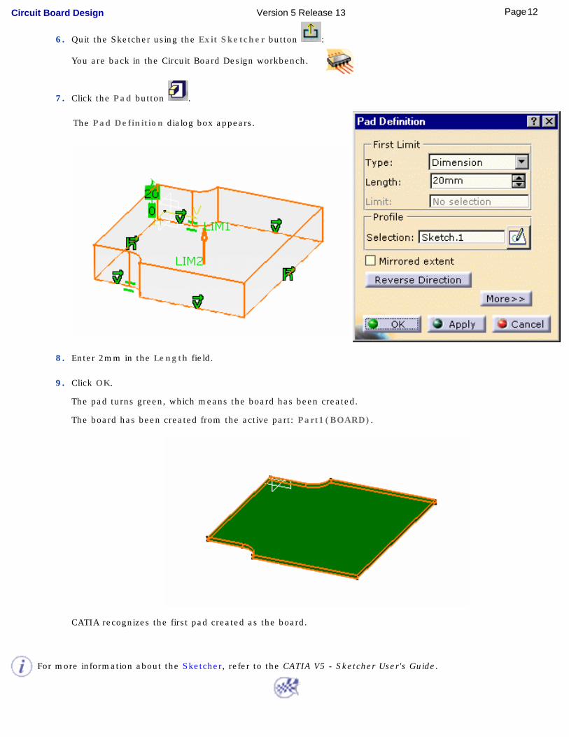
6. Quit the Sketcher using the Exit Sketcher button :
You are back in the Circuit Board Design workbench.
7. Click the Pad button .
The Pad Definition dialog box appears.
8. Enter 2mm in the Length field.
9. Click OK.
The pad turns green, which means the board has been created.
The board has been created from the active part: Part1(BOARD).
CATIA recognizes the first pad created as the board.
For more information about the Sketcher, refer to the CATIA V5 - Sketcher User's Guide.
12Page Circuit Board Design Version 5 Release 13

Creating a Pocket and Holes
This task shows how to create a pocket and two holes.
1. Sketch the contour of the pocket.
To do so:
a. click the Sketcher button
b. select the board to define the working plane
c. click the Profile button and draw the contour
d. then click the Exit Sketcher button to return to the 3D world.
● Click the Pocket button .The Pocket Definition dialog box is displayed and CATIA previews a pocket with default parameters.
● Set the Up to last option to define the pocket limit.
14Page Circuit Board Design Version 5 Release 13

This means that the application will extend the pocket to the last possible face, that is the pad bottom.
● Click OK.
● Click the Hole button .
● Select the board to define the working plane.
The Hole Definition dialog box appears.
CATIA previews the hole to be created with default parameters.
● Enter 4mm for the diameter and click OK.
The hole is created.
● Repeat the steps 5, 6 and 7 to drill the second hole.
The pocket and holes are added to the specification tree.
15Page Circuit Board Design Version 5 Release 13

16Page Circuit Board Design Version 5 Release 13

Creating a Constraint Area
This task shows you how to create constraint areas.The constraint areas belong to the board part in separate bodies.
1. Choose the Insert -> Body menu item.
2. Double-click to activate the newly created body.
3. Select the Sketcher button .
4. Select the board to define the working plane.
5. Click the Profile button and draw the following contour:
6. Click the Exit Sketcher button to return to the 3D world.
7. Click the Pad button .The Pad Definition dialog box appears.
8. Enter 1mm for the Length.
9. Click OK to validate.
10. Select the Constraint Area button .
17Page Circuit Board Design Version 5 Release 13

The Constraint Areas dialog box opens.
11. Choose the PLACE_OUTLINE type and click OK.The PLACE_OUTLINE area is displayed in transparency.
12. Repeat steps 1 to 10 to create another constraint area on the other face of the board according to the following contour:
18Page Circuit Board Design Version 5 Release 13
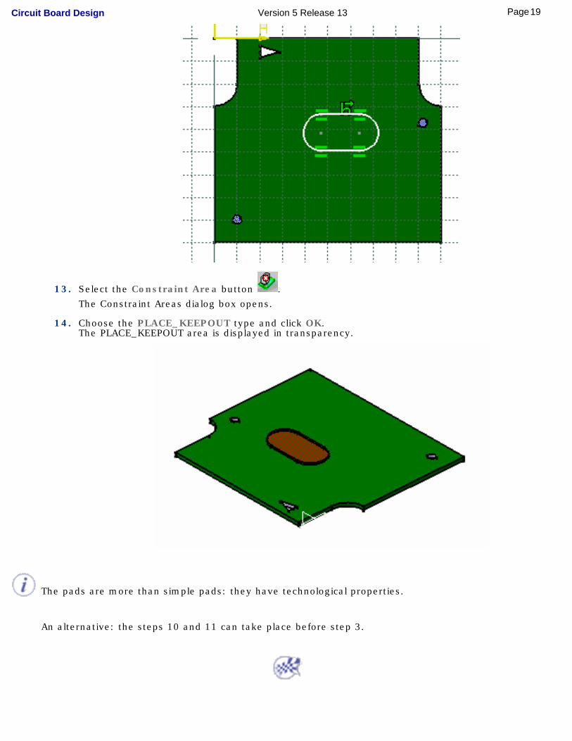
13. Select the Constraint Area button .The Constraint Areas dialog box opens.
14. Choose the PLACE_KEEPOUT type and click OK.The PLACE_KEEPOUT area is displayed in transparency.
The pads are more than simple pads: they have technological properties.
An alternative: the steps 10 and 11 can take place before step 3.
19Page Circuit Board Design Version 5 Release 13
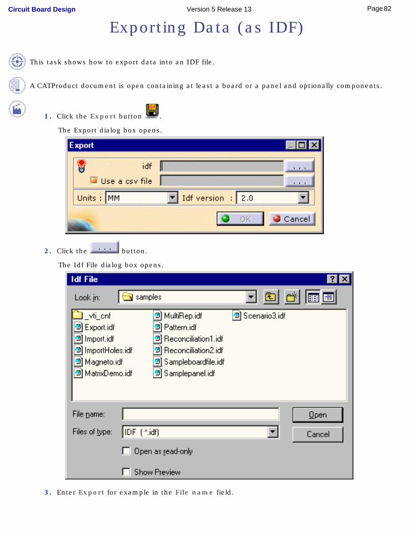
Exporting Data (as IDF)
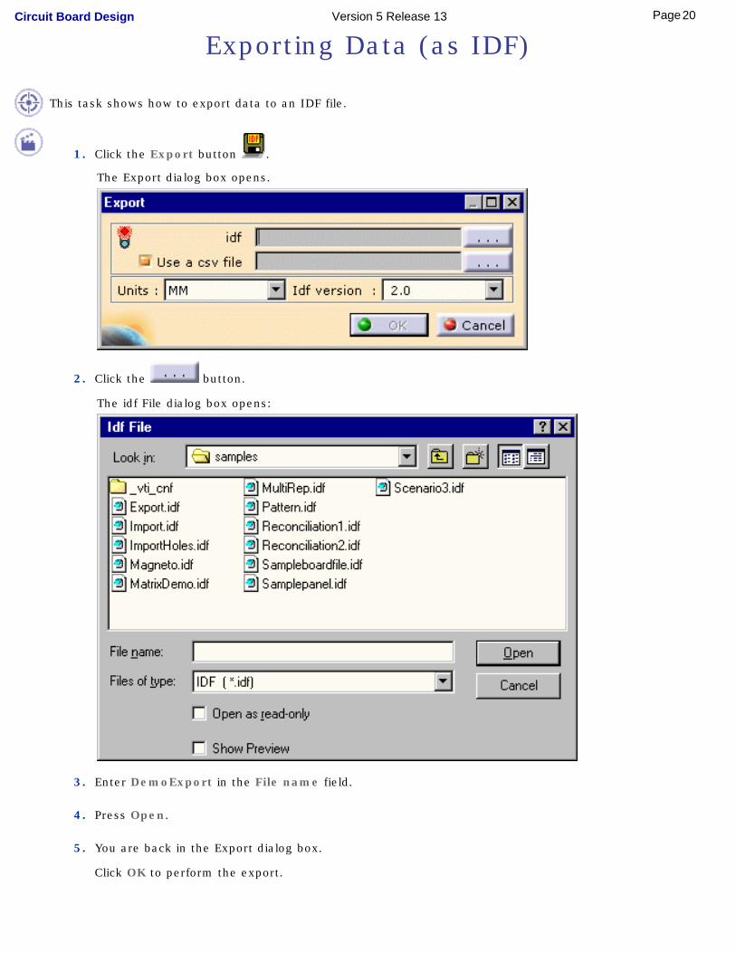
This task shows how to export data to an IDF file.
1. Click the Export button .
The Export dialog box opens.
2. Click the button.
The idf File dialog box opens:
3. Enter DemoExport in the File name field.
4. Press Open.
5. You are back in the Export dialog box.
Click OK to perform the export.
20Page Circuit Board Design Version 5 Release 13

An Information message is displayed:
6. Click OK to close the information window.
21Page Circuit Board Design Version 5 Release 13

Importing the IDF File
This task shows how to import the IDF data previously saved to a new document.You can also import IDF data from an ECAD system.
1. Select File -> Open in the menu bar.
The File Selection dialog box opens.
2. Select .idf in the Files of type field.
3. Select the DemoExport.idf file.
4. Press Open.
The Circuit Board Design Import window pops up.
The DemoExport.idf file is already selected.
5. Press OK.The Status bar shows the progression.The result should look like this:
22Page Circuit Board Design Version 5 Release 13
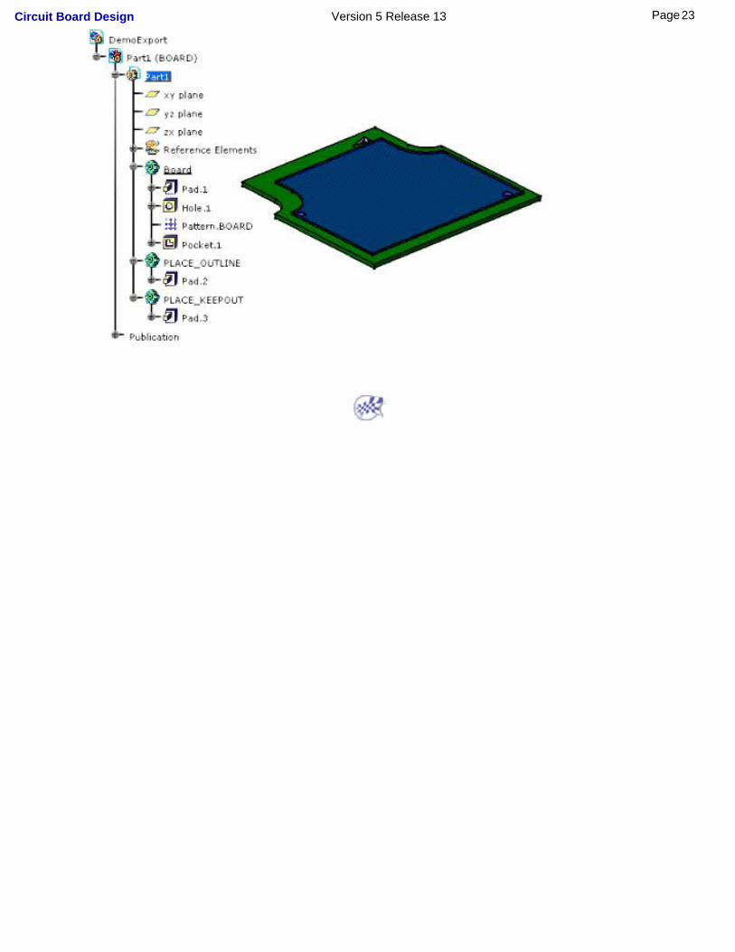
23Page Circuit Board Design Version 5 Release 13

User Tasks
The User Tasks section explains and illustrates how to create various kinds of features.
The table below lists the information you will find.
Accessing the Circuit Board WorkbenchCreating a Panel (IDF 3.0)
Creating a BoardConstraint Areas
Creating Pocket and HolesPatterns
Managing ComponentsExporting Data
ImportingWorking with CatalogsWorkbench Integration
Import in Context with Reconciliation
24Page Circuit Board Design Version 5 Release 13
Accessing the Circuit Board Workbench
This task explains how to set up the environment.
CATIA is launched. A CATProduct document is displayed.
Make sure the Product1 feature is highlighted before switching to another workbench.
1. Choose the Circuit Board Design item from the Start ->
Equipments & Systems menu.
The Circuit Board Design workbench is displayed and ready to use.
You can add the Circuit Board Design workbench to your Favorites, using the Tools -> Customize item. For more information, refer to CATIA V5 - Infrastructure User's Guide.
25Page Circuit Board Design Version 5 Release 13

Panel
Create from scratch: Sketch a profile to create a pad to be the panel.
Using an IDF file: Import the data from an IDF 3.0 file.
27Page Circuit Board Design Version 5 Release 13
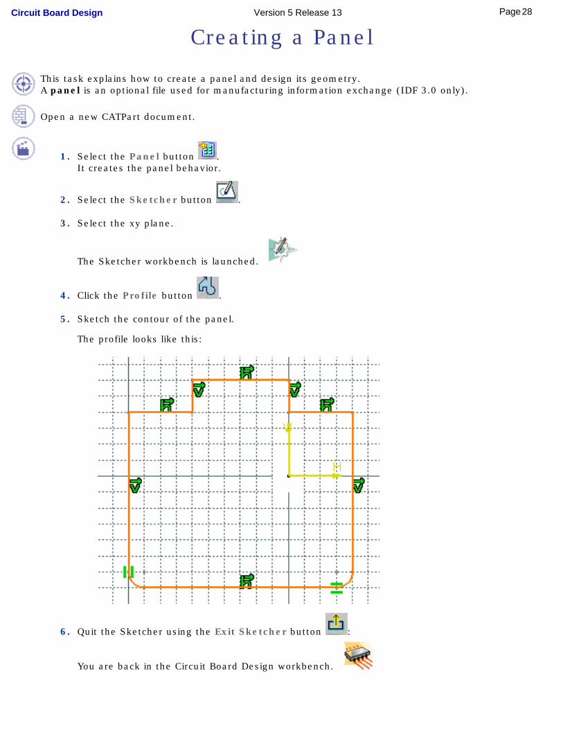
Creating a Panel
This task explains how to create a panel and design its geometry.A panel is an optional file used for manufacturing information exchange (IDF 3.0 only).
Open a new CATPart document.
1. Select the Panel button .It creates the panel behavior.
2. Select the Sketcher button .
3. Select the xy plane.
The Sketcher workbench is launched.
4. Click the Profile button .
5. Sketch the contour of the panel.
The profile looks like this:
6. Quit the Sketcher using the Exit Sketcher button :
You are back in the Circuit Board Design workbench.
28Page Circuit Board Design Version 5 Release 13

7. Click the Pad button .The Pad Definition dialog box appears.
8. Enter 2mm in the Length field.
9. Click OK.The pad turns "sea green", this means the panel representation has been created.The panel has been created from the active part: Part1.
By default, CATIA recognizes the first pad created as a panel.
For more information about the Sketcher, refer to the CATIA V5 - Sketcher User's Guide.
29Page Circuit Board Design Version 5 Release 13

Creating a Panel Using an IDF File
This task explains how to create a panel by importing an IDF (3.0) file.A panel is an optional file used for manufacturing information exchange (IDF 3.0 only).
You are working with the Circuit Board Design workbench.
1. Select the File -> Open menu.The File Selection dialog box opens.
2. Select the samplepanel.idf file.The Circuit Board Design Import dialog box opens:
Note that:
❍ an IDF file only contains the description of one panel or one board.
❍ when the panel import file also refers to a board, the board part number is indicated in the file. The Edit Links icon is enabled to let you find the board import files.
3. Click the Edit Links button .The Circuit Board Design dialog box opens:
4. Browse using the button to locate the board import files:
❍ Sampleboardfile.idf
❍ Sampleboard.lib
30Page Circuit Board Design Version 5 Release 13
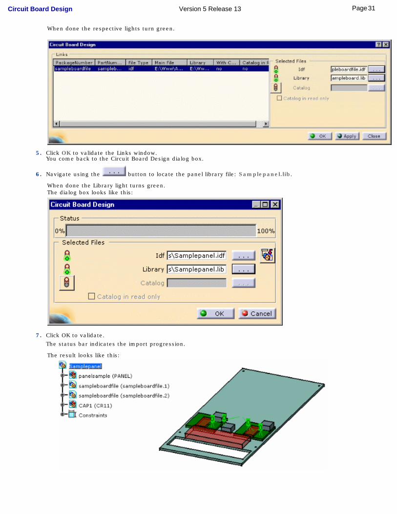
When done the respective lights turn green.
5. Click OK to validate the Links window.You come back to the Circuit Board Design dialog box.
6. Navigate using the button to locate the panel library file: Samplepanel.lib.
When done the Library light turns green.The dialog box looks like this:
7. Click OK to validate.The status bar indicates the import progression.
The result looks like this:
31Page Circuit Board Design Version 5 Release 13

You can also use catalog files for both the panel and board imports, if need be.
32Page Circuit Board Design Version 5 Release 13

Board
Create from scratch: Sketch a profile to create a pad to be the board.
Create from an existing part: In a CATPart document, select the pad to become the board.
Recognize in Assembly context: In a CATProduct document, select a previously created pad, possibly with holes and pockets. They all get technological properties.
33Page Circuit Board Design Version 5 Release 13

Create a Board From Scratch
This task explains how to create a board and design its geometry.
The Circuit Board Design functions are available when you are in the Part Design environment.Several functions are integrated from the Part Design workbench.
Choose the Circuit Board Design workbench. A new CATPart document opens.
1. Select the Create Board button .It creates the board behavior.
2. Select the Sketcher button .
3. Select the xy plane.
The Sketcher workbench is launched.
4. Click the Profile button .
5. Sketch the contour of the Board.
The profile looks like this:
6. Quit the Sketcher using the Exit button :
You are back in the Circuit Board Design workbench.
7. Click the Pad button .The Pad Definition dialog box appears.
34Page Circuit Board Design Version 5 Release 13

8. Enter 2mm in the Length field.
9. Click OK.The pad turns green, this means the board representation has been created.The board has been created from the active part: Part1.
By default, CATIA recognizes the first pad created as the Board.
For more information about the Sketcher, refer to the CATIA V5 - Sketcher User's Guide.
35Page Circuit Board Design Version 5 Release 13

From a Previously Created Part
This task shows how to create a board from an existing part.
Open the Scenario1.CATProduct document.It contains a part with two pads.
1. Click the Create Board button .The PartBody contains two pads, so you have to select the pad which will represent the board.
2. Select Pad.1.CATIA recognizes the board and displays it in green.You can add holes, pockets and constraint areas, as well as technological properties
36Page Circuit Board Design Version 5 Release 13

Automatic Recognitionin Assembly Context
This task illustrates how Circuit Board features are automatically recognized.
Open the Scenario2.CATProduct document.It contains a part with a pad, holes and a pocket.
1. Double-click to activate Part1.
2. Click the Create Board button .You are prompted to select a pad for the board representation.
3. Select Pad.1.The board turns green.
4. Right-click the instance of the board: Part1 (Part1.1)and select the Properties item.Click the More... button. Select the board or the holes in the specification tree.
The objects (board and holes) have automatically acquired technological properties:
38Page Circuit Board Design Version 5 Release 13

5. Select the Export button .The Export dialog box pops up. Select an IDF file.A board is recognized, all the related features are taken into account and exported to the IDF file.
6. Open the .idf file as a text file. It looks like this:
39Page Circuit Board Design Version 5 Release 13

Constraint Area
Sketch a profile to create a pad and assign it to the Constraint Area.
Create a Multi-Domain Constraint Area.
Add technological Properties to the constraint area.
Use the Settings to change the Constraint Area default colors.
40Page Circuit Board Design Version 5 Release 13

Creating a Constraint Area
This task shows you how to create a constraint area.
A constraint area is a space reservation used for different purposes such as allowing/forbidding the routing or placing
of components etc.
This feature is available on both the board and the manufacturing panel.
Open a CATProduct document, containing a board.
1. Choose the Insert -> Body menu item (optional).Body.2 is created, belonging to the interactive board component.
2. Select the Sketcher button .
3. Select the board to define the working plane.
4. Click the Profile button and draw the contour of the constraint area.
5. Click the Exit Sketcher button to return to the 3D world.
6. Click the Pad button .The Pad Definition dialog box appears.
7. Enter 5mm in the Length field.
41Page Circuit Board Design Version 5 Release 13
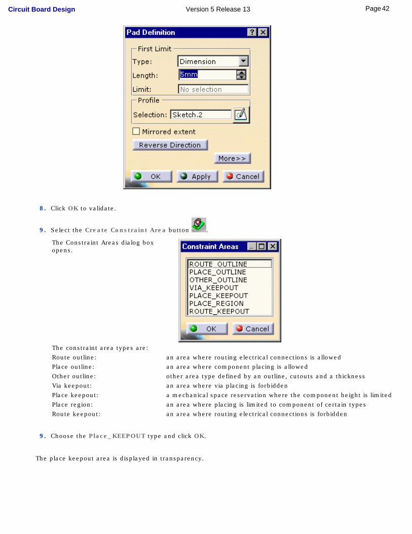
8. Click OK to validate.
9. Select the Create Constraint Area button .
The Constraint Areas dialog box opens.
The constraint area types are:Route outline: an area where routing electrical connections is allowedPlace outline: an area where component placing is allowedOther outline: other area type defined by an outline, cutouts and a thicknessVia keepout: an area where via placing is forbiddenPlace keepout: a mechanical space reservation where the component height is limitedPlace region: an area where placing is limited to component of certain typesRoute keepout: an area where routing electrical connections is forbidden
9. Choose the Place_KEEPOUT type and click OK.
The place keepout area is displayed in transparency.
42Page Circuit Board Design Version 5 Release 13

The pad is more than a simple pad: it has technological properties.
When you create a constraint area interactively, the body is not automatically renamed with the constraint area type (as it works on import). However, you can change its name using the Properties contextual menu.
43Page Circuit Board Design Version 5 Release 13

Creating a Multi-Domain Constraint Area
This task shows you how to create a multi-domain constraint area.
A multi-domain constraint area is a space reservation made up of several elements in the same body. Each multi-domain constraint area belongs to a separate body under the PartBody.This feature is available on both the board and manufacturing panel.
Open a CATProduct document, containing a board/panel.
1. Choose the Insert -> Body menu item.
2. Select the Sketcher button .
3. Select the board/panel to define the working plane.
4. Click the Profile button and draw the multiple contour of the constraint area.
5. Click the Exit Sketcher button to return to the 3D world.
6. Click the Pad button .The Pad Definition dialog box appears.
7. Enter 8mm in the Length field.
44Page Circuit Board Design Version 5 Release 13

8. Click OK to validate.
9. Select the Constraint Area button .
The Constraint Areas dialog box opens.
The constraint area types are:Route outline: an area where routing electrical connections is allowedPlace outline: an area where component placing is allowedOther outline: other area type defined by an outline, cutouts and a thicknessVia keepout: an area where via placing is forbiddenPlace keepout: a mechanical space reservation where the component height is limitedPlace region: an area where placing is limited to component of certain typesRoute keepout: an area where routing electrical connections is forbidden
9. Choose the type and click OK.
The multi-domain constrain area is displayed in transparency.
45Page Circuit Board Design Version 5 Release 13

The pads are more than simple pads: they have technological properties.
46Page Circuit Board Design Version 5 Release 13
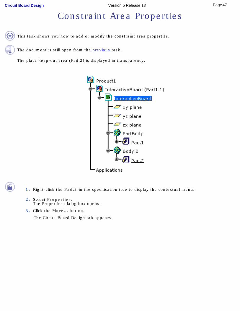
Constraint Area Properties
This task shows you how to add or modify the constraint area properties.
The document is still open from the previous task.
The place keep-out area (Pad.2) is displayed in transparency.
1. Right-click the Pad.2 in the specification tree to display the contextual menu.
2. Select Properties.The Properties dialog box opens.
3. Click the More... button.
The Circuit Board Design tab appears.
47Page Circuit Board Design Version 5 Release 13

4. Select the Circuit Board Design tab.
The constraint area properties are displayed:
48Page Circuit Board Design Version 5 Release 13

Note that some of the attributes are displayed but cannot be modified:❍ the constraint area subtype
❍ the constraint area position: TOP or BOTTOM
5. Enter 6mm in the Maximal height field and 2mm in the Minimal height field.
6. Then click OK.The pad is updated: the maximal and minimal heights are linked to the pad limits.It represents the overall dimensions of the constraint area.
A constraint area may have a representation on both faces of the board.This attribute is recognized and displayed in the Circuit Board Design tab.This attribute is managed only on the idf file import.
In the specification tree, such a constraint area (BOTH) is represented by two pads in the same body.They share the same properties: modifying the properties on one pad will modify them on the other pad.
49Page Circuit Board Design Version 5 Release 13

50Page Circuit Board Design Version 5 Release 13

Changing the Constraint AreasColor Settings
This task shows you how to change the user settings. These are permanent settings.
1. Select the Tools -> Options menu.The Options dialog box opens.
2. Click Equipments & Systems in the left-hand box.
3. Click the Circuit Board Design workbench:
The Graphic tab is displayed.
❍ You can set the color of your choice to the different areas.If you tick the Update documents in session box, your change will be applied to the current document.
4. Click OK to validate.
51Page Circuit Board Design Version 5 Release 13

Creating a Pocket and Holes
This task shows how to create a pocket and holes, with technological properties.
These features are available on both the board and the manufacturing panel.
Open a CATProduct document containing a board.
1. Sketch the contour of the pocket.
To do so:
a. click the Sketcher button
b. select the board to define the working plane
c. click the Profile button and draw the contour around the motor
d. then click the Exit Sketcher button to return to the 3D world.
53Page Circuit Board Design Version 5 Release 13
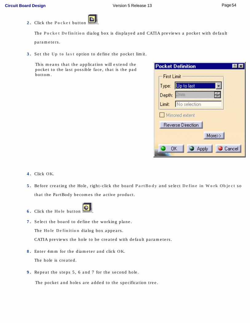
2. Click the Pocket button .
The Pocket Definition dialog box is displayed and CATIA previews a pocket with default
parameters.
3. Set the Up to last option to define the pocket limit.
This means that the application will extend the pocket to the last possible face, that is the pad bottom.
4. Click OK.
5. Before creating the Hole, right-click the board PartBody and select Define in Work Object so
that the PartBody becomes the active product.
6. Click the Hole button .
7. Select the board to define the working plane.
The Hole Definition dialog box appears.
CATIA previews the hole to be created with default parameters.
8. Enter 4mm for the diameter and click OK.
The hole is created.
9. Repeat the steps 5, 6 and 7 for the second hole.
The pocket and holes are added to the specification tree.
54Page Circuit Board Design Version 5 Release 13

10. Right-click the Hole.1 in the specification tree to display the contextual menu.
11. Select Properties.
The Properties dialog box opens.
12. Click the More... button.
13. Select the Circuit Board tab.
14. Switch the Subtype to NPTH (non conductive) and click OK.
The hole is more than a simple hole: it has a technological property.
15. Repeat the steps 9 to 13 for the second hole.
These holes are used for mounting purposes.
55Page Circuit Board Design Version 5 Release 13

Patterns
Create a hole then define a pattern.
Create a hole, a pattern then define a pattern of pattern.
Pattern Usage During Import: if a component uses a pattern for mounting purpose, the pattern is recognized during import.Move/Delete Component Using a Pattern: move or delete the holes associated.
Delete Pattern: delete the holes associated.
57Page Circuit Board Design Version 5 Release 13

Pattern Designfor Hole or Cutout
This task shows you how to create a pattern for holes or cutouts.Patterns are often used for mounting purpose.
This feature is available on both the board and manufacturing panel.
Open a new CATProduct document and create a board.
1. Select the Hole button to create the hole to be patterned.
2. Select the Rectangular Pattern button .
3. Select the hole to pattern.The Rectangular Pattern Definition dialog box opens.
58Page Circuit Board Design Version 5 Release 13

Enter the following values for the first direction:
❍ Instances: 6
❍ Spacing: 10mm
❍ Reference Direction: select the bottom edge (Edge.1)
❍ Reverse the direction.
For the second direction:
❍ Instances: 2
❍ Spacing: 20mm
❍ Reference Direction: select the left edge (Edge.2)
4. Click OK to validate.The pattern is added to the specification tree and the result looks like this:
Note that the properties of the original hole (or cutout) are extended to the pattern.
For more information about patterns, refer to CATIA - Part Design.
59Page Circuit Board Design Version 5 Release 13

Pattern of Pattern
This task shows you how to create a pattern of pattern.Patterns are often used for mounting purpose.
This feature is available for both the board and the manufacturing panel.
Open the InteractiveBoard.CATPart document.
1. Select the Rectangular Pattern icon to create the pattern.
2. Select the Pattern.BOARD either in the specification tree or in the geometry.The Rectangular Pattern Definition dialog box opens.
Enter the following values for the first direction:
❍ Instances: 3
❍ Spacing: 40mm
❍ Reference Direction: select the bottom edge (Edge.3)
61Page Circuit Board Design Version 5 Release 13
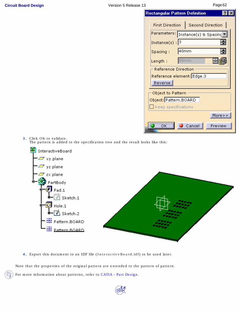
3. Click OK to validate.The pattern is added to the specification tree and the result looks like this:
4. Export this document to an IDF file (InteractiveBoard.idf) to be used later.
Note that the properties of the original pattern are extended to the pattern of pattern.
For more information about patterns, refer to CATIA - Part Design.
62Page Circuit Board Design Version 5 Release 13

Pattern Usage During Import
This task shows you that the rectangular pattern used for mounting a component, is recognized during import.
This feature is available on both the board and manufacturing panel.
Before starting, set the Tools -> Options -> Infrastructure -> Part as shown below:
1. Open the Pattern.idf document from the samples directory.
The Circuit Board Design Import dialog box opens.
2. Click to activate the Catalog light.
3. Browse to select the Pattern.catalog.
The Catalog light becomes green.
4. Click OK to validate.
A message informs you that the catalog is unchanged (it is in read only mode).
The import result looks like this:
64Page Circuit Board Design Version 5 Release 13

The idf file contains the board, the component and the holes. During the import, the holes coordinates are analyzed and recognized as defining a pattern. If you move or delete the component, the pattern will be updated (see the next task).
65Page Circuit Board Design Version 5 Release 13

Move Pattern
This task shows you how the pattern is modified when a component using this pattern is moved or deleted.
The document is still open from the previous task.
1. Switch to the Assembly Design workbench.
2. Select the Manipulation button .The Manipulation Parameters dialog box opens.
3. Select the Drag along any plane button.
4. Move the component to the top left corner.
66Page Circuit Board Design Version 5 Release 13
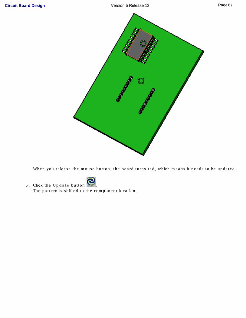
When you release the mouse button, the board turns red, which means it needs to be updated.
5. Click the Update button .The pattern is shifted to the component location.
67Page Circuit Board Design Version 5 Release 13

68Page Circuit Board Design Version 5 Release 13
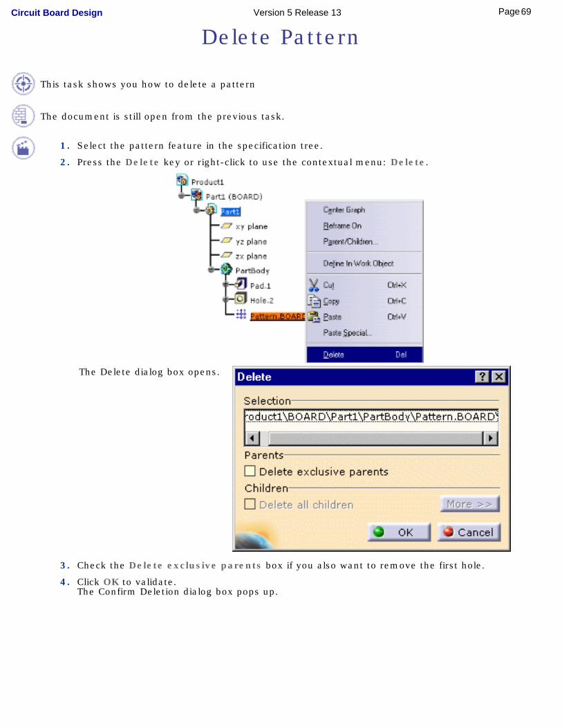
Delete Pattern
This task shows you how to delete a pattern
The document is still open from the previous task.
1. Select the pattern feature in the specification tree.
2. Press the Delete key or right-click to use the contextual menu: Delete.
The Delete dialog box opens.
3. Check the Delete exclusive parents box if you also want to remove the first hole.
4. Click OK to validate.The Confirm Deletion dialog box pops up.
69Page Circuit Board Design Version 5 Release 13

5. Press Yes to confirm the deletion.The pattern has been removed.
70Page Circuit Board Design Version 5 Release 13

Components
Create: Click this button, enter a package number then select the pad to become the component.
Multi-representation: The multiple representations associated to an electronic component are handled through the catalog.Properties: Right-click the component to browse its technological properties.
Constraints: Double-click a constraint to edit the component status.
71Page Circuit Board Design Version 5 Release 13
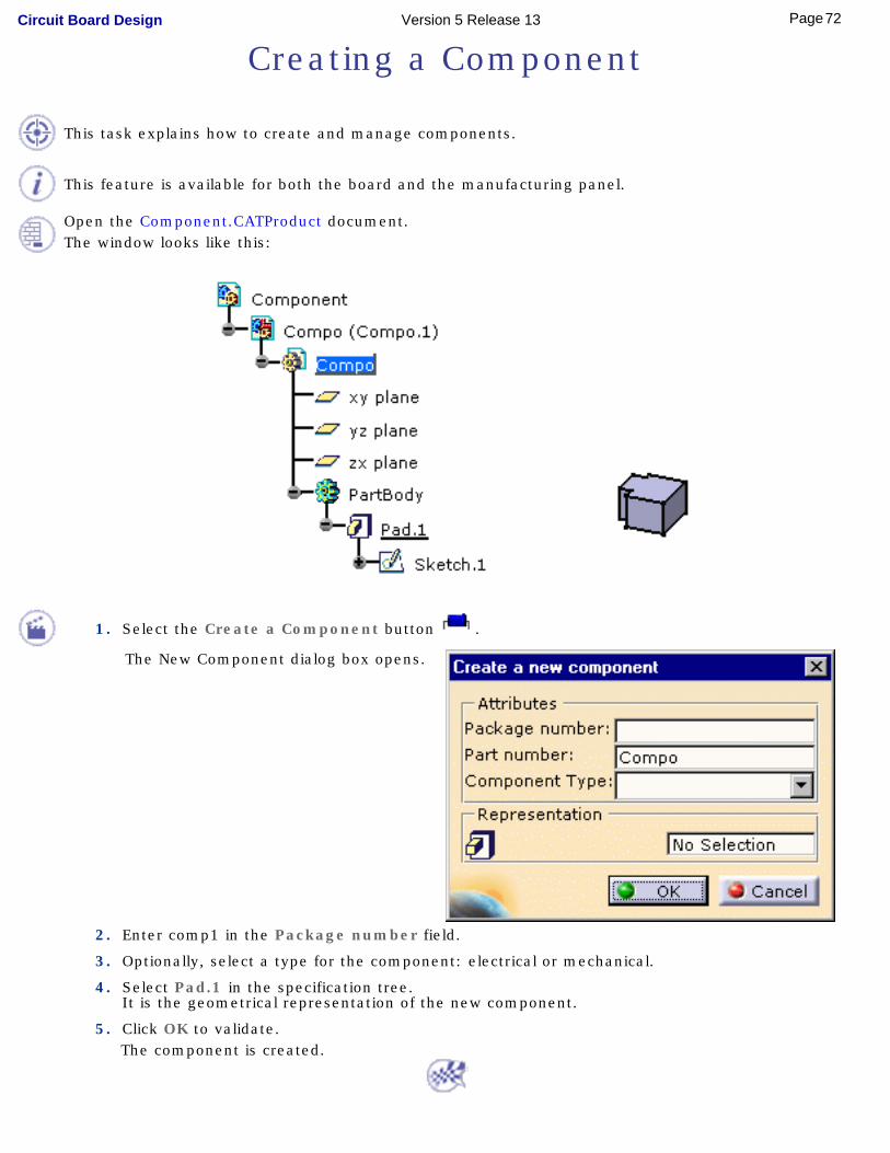
Creating a Component
This task explains how to create and manage components.
This feature is available for both the board and the manufacturing panel.
Open the Component.CATProduct document.The window looks like this:
1. Select the Create a Component button .
The New Component dialog box opens.
2. Enter comp1 in the Package number field.
3. Optionally, select a type for the component: electrical or mechanical.
4. Select Pad.1 in the specification tree. It is the geometrical representation of the new component.
5. Click OK to validate.The component is created.
72Page Circuit Board Design Version 5 Release 13

Multi-Representation Management
The multiple representations associated to an electronic component are handled through the catalog: users can choose a dedicated representation for a given electronic component either at the import process or at the component pre-placement. For example, amongst dedicated representations, users can select a simplified representation or an exact one.
1. Open the MultiRep.idf document from the samples folder.
The Circuit Board Design Import dialog box opens. ❍ Select MultiRep.lib for the library
❍ Create a new catalog in read/write mode: MultiRep.catalog
❍ Click OK to validate.
The import is performed.
2. Open the MultiRep.catalog in the Catalog Editor.
74Page Circuit Board Design Version 5 Release 13

❍ Two component references with the same PartNumber but different representations (PackageNumber) are stored in the catalog.
❍ During the import process, the PartNumber must be unique.When the assembly is generated, if several components have the same PartNumber but different representations, the PartNumber of the second and following instances is automatically renamed with the instance name.
In the catalog:
● the PartNumber identifies the component
● the PackageNumber identifies the representations associated to a component
● the Instance Name identifies the instance within the assembly.
75Page Circuit Board Design Version 5 Release 13
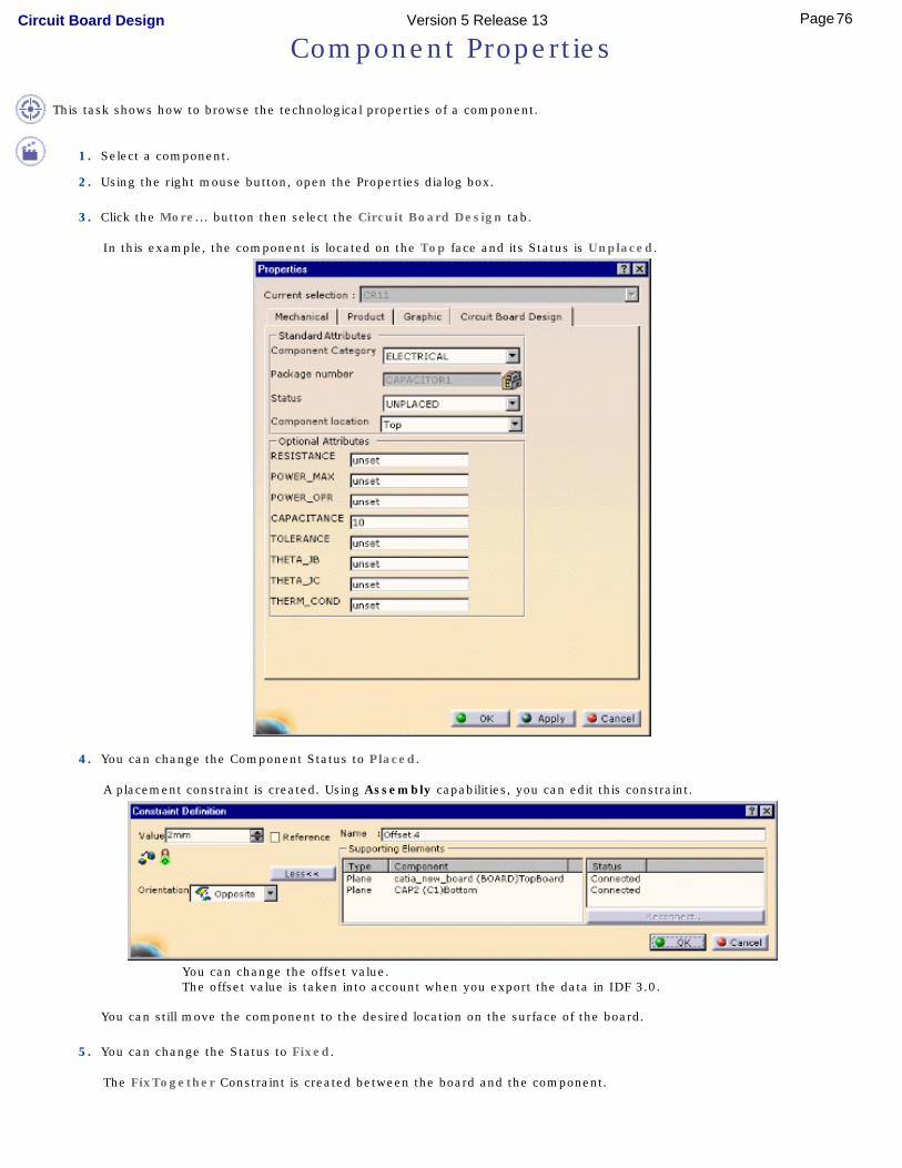
Component Properties
This task shows how to browse the technological properties of a component.
1. Select a component.
2. Using the right mouse button, open the Properties dialog box.
3. Click the More... button then select the Circuit Board Design tab.
In this example, the component is located on the Top face and its Status is Unplaced.
4. You can change the Component Status to Placed.
A placement constraint is created. Using Assembly capabilities, you can edit this constraint.
You can change the offset value.The offset value is taken into account when you export the data in IDF 3.0.
You can still move the component to the desired location on the surface of the board.
5. You can change the Status to Fixed.
The FixTogether Constraint is created between the board and the component.
76Page Circuit Board Design Version 5 Release 13

6. Other properties come up with IDF 3.0 file support such as:
Optional Attributes:❍ Capacitance
❍ Resistance
❍ Tolerance
❍ etc.
as well as user defined attributes (optional).They can be valuated in this dialog box.
7. Click OK to validate.
77Page Circuit Board Design Version 5 Release 13

Components and Constraints
This task explains how to manage components given the component constraint type.
This feature is available on both the board and the manufacturing panel.
Open the Scenario3.idf file and the corresponding Scenario3.lib file from the samples folder.
An Assembly Product document is generated.
If the configuration you are using provides access to the Assembly Design workbench, geometrical constraints
are created between the board and the components, and are displayed.
Within the assembly, the board needs to be anchored.
78Page Circuit Board Design Version 5 Release 13

1. Double-click the power-jack constraint shown here in red.
The Constraint Definition dialog box opens.
The Assembly constraints (geometrical constraints) linking the components to the board depend on the
component status.
Component Status Assembly Constraint
Unplaced No Constraint
Placed Plane to Plane Constraint
Fixed Fixity Constraint
This information is transmitted through the import file (.idf), the component capability to change location is then driven by the constraint.
Under certain circumstances, a component status can be modified:
● from unplaced to placed or fixed
● from placed to fixed
but never from fixed to placed or unplaced, nor from placed to unplaced (in order to keep the information defined in the ECAD world).
79Page Circuit Board Design Version 5 Release 13

2. Editing the constraint, using the More>> button, lets you modify the offset between the component
and the board (IDF 3.0):
The IDF 3.0 takes into account the offset which represents a mounting constraint of the component onto the board.
The offset is also managed between the board and the panel.
80Page Circuit Board Design Version 5 Release 13
Export
Exporting Data: export a board and components respecting an assembly context
IDF 3.0: sums-up the information added to the export file when using IDF 3.0.
81Page Circuit Board Design Version 5 Release 13
Exporting Data (as IDF)
This task shows how to export data into an IDF file.
A CATProduct document is open containing at least a board or a panel and optionally components.
1. Click the Export button .
The Export dialog box opens.
2. Click the button.
The Idf File dialog box opens.
3. Enter Export for example in the File name field.
82Page Circuit Board Design Version 5 Release 13
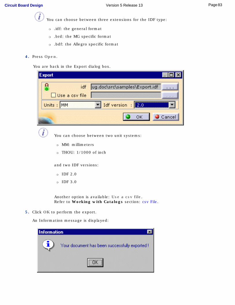
You can choose between three extensions for the IDF type:
❍ .idf: the general format
❍ .brd: the MG specific format
❍ .bdf: the Allegro specific format
4. Press Open.
You are back in the Export dialog box.
You can choose between two unit systems:
❍ MM: millimeters
❍ THOU: 1/1000 of inch
and two IDF versions:
❍ IDF 2.0
❍ IDF 3.0
Another option is available: Use a csv file.Refer to Working with Catalogs section: csv File.
5. Click OK to perform the export.
An Information message is displayed:
83Page Circuit Board Design Version 5 Release 13

To be exported to an IDF file, the document must contain at least a board or a panel. Other objects are
also exported:
● components
● constraint areas including multi-domain ones
● holes
● cutouts
● patterns of holes or cutouts including patterns of pattern (one level).
84Page Circuit Board Design Version 5 Release 13

IDF 3.0
This file sums-up what information is managed in the export file when using IDF 3.0.
1. Manufacturing panel information: the panel file is an optional file.
The panel file contains the physical description of the manufacturing panel and the location of the
boards and components on that panel. It can be created interactively then exported.
2. Annotations: a new section is added to the file.
It contains notes for the design that can be displayed to allow the electrical and mechanical
designers to communicate additional information about the design entities. They are not intended
for manufacturing purpose. At the moment, they can only be modified in CATIA then exported.
3. Offset: the offset field represents the mounting offset for a component onto the board.
It is also available for board mounting offset onto the panel.
Placing a component creates a constraint. Editing the constraint allows you to modify the offset.
It will be taken into account in the export file.
4. Properties: an optional record specifies properties for the component such as capacitance,
resistance, tolerance, power_max, etc. as well as user defined attributes.
You can set the values in the Properties dialog box. Your changes will be taken into account in
the export file.
85Page Circuit Board Design Version 5 Release 13

Import
Open an IDF File: import a board and components from an IDF file.
Import in Context: import a board and components respecting an assembly context
IDF 3.0: what is managed during IDF 3.0 import
File Extension Management during import
Error File Report when the import does not operate properly.
Annotation Management: can be modified in CATIA.
Filter on Holes: reduce the processing time.
Drill Holes: perform the drilling according to the display
86Page Circuit Board Design Version 5 Release 13
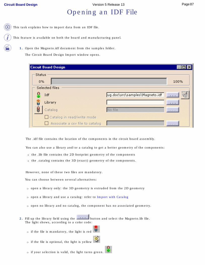
Opening an IDF File
This task explains how to import data from an IDF file.
This feature is available on both the board and manufacturing panel.
1. Open the Magneto.idf document from the samples folder.
The Circuit Board Design Import window opens.
The .idf file contains the location of the components in the circuit board assembly.
You can also use a library and/or a catalog to get a better geometry of the components:
❍ the .lib file contains the 2D footprint geometry of the components
❍ the .catalog contains the 3D (exact) geometry of the components.
However, none of these two files are mandatory.
You can choose between several alternatives:
❍ open a library only: the 3D geometry is extruded from the 2D geometry
❍ open a library and use a catalog: refer to Import with Catalog
❍ open no library and no catalog, the component has no associated geometry.
2. Fill up the library field using the button and select the Magneto.lib file.The light shows, according to a color code:
❍ if the file is mandatory, the light is red
❍ if the file is optional, the light is yellow
❍ if your selection is valid, the light turns green.
87Page Circuit Board Design Version 5 Release 13

3. Click OK to validate.The Status bar indicates the progression.The result looks as follows.
88Page Circuit Board Design Version 5 Release 13

Importing in Context
This task explains how to import circuit board elements and place them in context.
This feature is available for both the board and manufacturing panel.
Open the Context.CATProduct document.
1. Double-click to activate Product1.
2. Enter the Circuit Board Design workbench using the Start -> Equipments & Systems menu.
A new part is created.
3. Select the Import in Context icon .
4. Select the plane where you want to place the board and components, that is to say the CD bottom plane.
The Circuit Board Design dialog box is displayed.
5. Click the button to choose Scenario3.idf file and Scenario3.lib file in the respective fields.
It looks like this:
89Page Circuit Board Design Version 5 Release 13

Note: no catalog is used in this scenario.
6. Click OK to launch the import.The Status bar indicates the progression.
The result should look like this:
90Page Circuit Board Design Version 5 Release 13
IDF 3.0
This file sums-up what information is added to the import file when using IDF 3.0.
1. Manufacturing panel information: the panel file is an optional file.
It has been added (comparatively to IDF 2.0) to allow the exchange of manufacturing panel
information. The panel file contains the physical description of the manufacturing panel and the
location of the boards and components on that panel.
2. Annotations: a new section is added to the file.
It contains notes for the design that can be displayed to allow the electrical and mechanical
designers to communicate additional information about the design entities. They are not intended
for manufacturing purpose.
3. Offset: the offset field represents the mounting offset for a component onto the board.
It is also available for board mounting offset onto the panel.
4. Properties: an optional record specifies properties for the component such as capacitance,
resistance, tolerance, power_max, etc. as well as user defined attributes.
91Page Circuit Board Design Version 5 Release 13
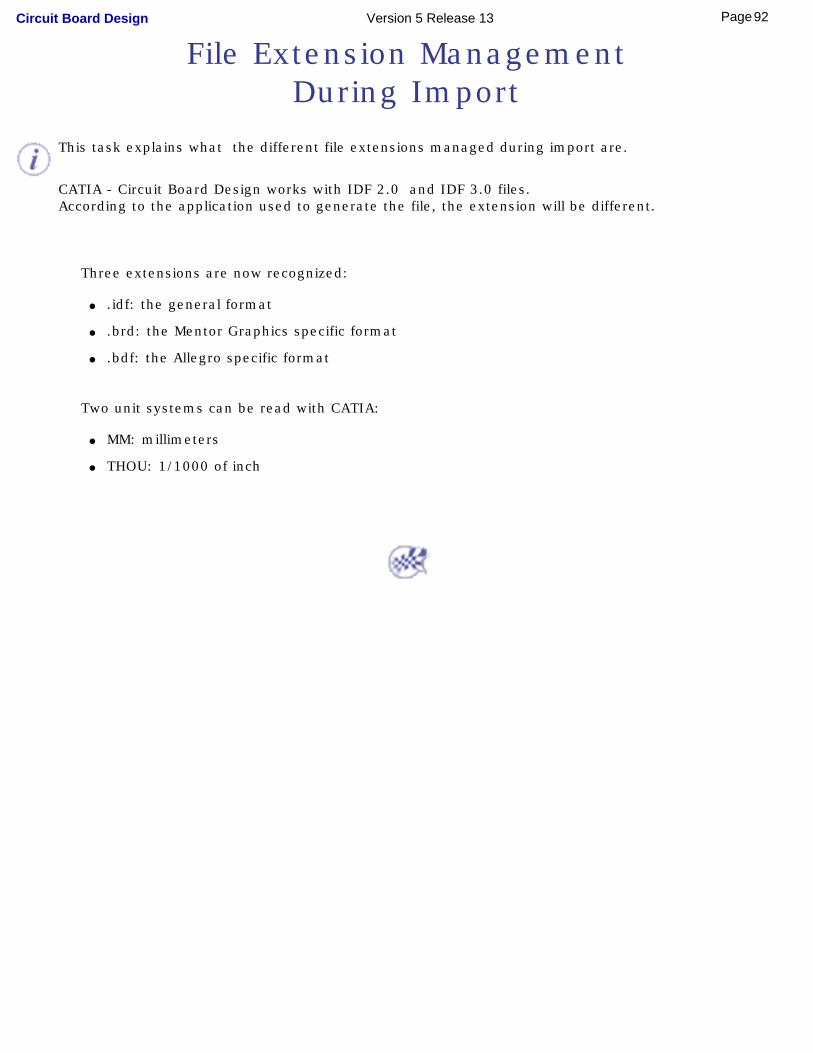
File Extension ManagementDuring Import
This task explains what the different file extensions managed during import are.
CATIA - Circuit Board Design works with IDF 2.0 and IDF 3.0 files.According to the application used to generate the file, the extension will be different.
Three extensions are now recognized:
● .idf: the general format
● .brd: the Mentor Graphics specific format
● .bdf: the Allegro specific format
Two unit systems can be read with CATIA:
● MM: millimeters
● THOU: 1/1000 of inch
92Page Circuit Board Design Version 5 Release 13

Error File Reporting
This task explains what happens when the file import does not operate properly.
The scenario is described in Opening an IDF File.
If a problem is detected during the import, the import operation continues and the items generating errors are listed in a report file:
The CATProduct resulting from the import is incomplete, that is to say that some components or areas or parts of the board can be missing or incomplete but the import itself has finished.
93Page Circuit Board Design Version 5 Release 13

Annotations Management
This task shows how to modify annotations after an import using IDF 3.0.
You have performed the panel import.
1. Select an Annotation in the specification tree.
The annotation is displayed on the constraint area.
2. Double-click the annotation.
It shows six parameters. Three of them can be modified in this version:❍ the text position (X and Y)
❍ the text.
94Page Circuit Board Design Version 5 Release 13

3. Double-click the Text parameter.
The Edit Parameter dialog box opens:
4. You can change the text of the annotation and click OK.
5. You can do the same for the text position by modifying the X or Y coordinates.
These modifications are taken into account when exporting data in an IDF file.
95Page Circuit Board Design Version 5 Release 13

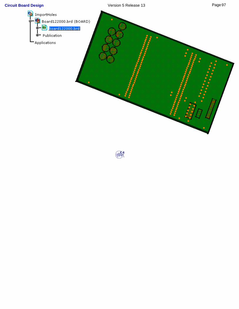
Filter on Holes During Import
This task explains the different ways to import holes according to your need and to reduce the processing time.
This feature is available on both the board and the manufacturing panel.
1. Open an idf file containing holes.
The Circuit Board Design Import window opens.
The different holes options are:❍ Draw only: the holes are not drilled but the contour is displayed in the geometry (default option)
❍ Drill all: the holes are drilled.
❍ Custom: ■ Drill only mounting (MNTG) and tooling (TLG) holes: only mounting and tooling holes are drilled, other holes are
displayed.
■ Diameter limit: drills the holes which diameter is superior to the given value.
■ User rule: gives access to the rule editor.To know how to write a rule, refer to CATIA - Knowledge Advisor User's Guide
2. Select the option of interest, in our case: Draw only.
3. Click OK to validate.
The import is performed and the result looks like this:
96Page Circuit Board Design Version 5 Release 13
97Page Circuit Board Design Version 5 Release 13

Drill Holes After Import
This task shows how to perform the drilling of the selected contours to obtain holes.
This feature is available on both the board and the manufacturing panel imported using an idf file.
An idf file has been imported using the holes option Draw only.
The result looks like this:
1. Expand the specification tree to display the CBD Holes.
98Page Circuit Board Design Version 5 Release 13

2. Click or Ctrl-click one or more Hole object in the specification tree.
3. Click the Drill selected holes button
or
Right-click to display the contextual menu and select the Drill holes item.
99Page Circuit Board Design Version 5 Release 13

The selected holes are drilled.
Note that:
In the specification tree:● The holes you have just drilled are no longer in the CBD Holes
container.
● They are now under the Board as:
100Page Circuit Board Design Version 5 Release 13

In the geometry:
The holes are drilled and not only displayed.
101Page Circuit Board Design Version 5 Release 13

Using Catalogs
Export a Component: open or create the catalog to store the component.
File -> Open Import: operate with a library and/or a catalog to get a better geometry of the components.
Access to the Catalog Editor to insert a component.
Using a csv file.
102Page Circuit Board Design Version 5 Release 13

Export a Component
This task explains how to create a catalog for circuit board components.
This feature is available for both the board and the manufacturing panel.
Open the Component2.CATProduct document.
1. Double-click to activate the component.
2. Select the Export a Component button .
The Component Storage window pops up:
3. Click the Browse button to select the catalog:
The Catalog dialog box opens.
103Page Circuit Board Design Version 5 Release 13
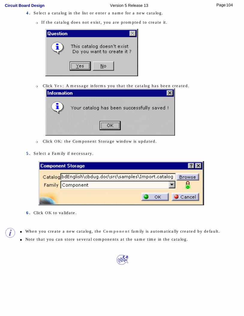
4. Select a catalog in the list or enter a name for a new catalog.
❍ If the catalog does not exist, you are prompted to create it.
❍ Click Yes: A message informs you that the catalog has been created.
❍ Click OK: the Component Storage window is updated.
5. Select a Family if necessary.
6. Click OK to validate.
● When you create a new catalog, the Component family is automatically created by default.
● Note that you can store several components at the same time in the catalog.
104Page Circuit Board Design Version 5 Release 13

Importing Using a Catalog
This task explains how to import data from an IDF file, where the component 3D geometry is imported from a catalog.
This feature is available for both the board and the manufacturing panel.
1. Open the Import.idf document from the sample directory.
The .idf file contains the location of the components in the circuit board assembly.
You can use a library and/or a catalog to get a better geometry of the components: ● the .lib file contains the 2D footprint geometry of the components.
● the .catalog contains the 3D (exact) geometry of the components.
However, none of these files are mandatory.
You can choose between several alternatives:
● open a library only: the 3D geometry is extruded from the 2D geometry
● open a library and use an existing catalog: ❍ the component exists in the catalog, its 3D geometry is imported from the catalog
❍ the component does not exist in the catalog, it is extruded from the 2D geometry and stored in the catalog if the catalog is not protected (Catalog in read/write mode box is not checked)
● open a library and a new catalog: the 3D geometry is extruded from the 2D geometry and stored in the newly created catalog
● open no library, but a catalog: ❍ the component exists in the catalog, its 3D geometry is imported from the catalog
❍ the component does not exist in the catalog, it is created with no associated geometry
● open neither library nor catalog, the component has no associated geometry.
The Circuit Board Design dialog box opens.
The first light is green: the selection is valid.
The second light is yellow: you can choose a library (optional).
105Page Circuit Board Design Version 5 Release 13

Note: If no components are available in the idf file, the light does not show any color.
2. Browse using the button and select the ImportComps.lib file.The light turns green.
3. Click to activate the third light: it turns yellow and the catalog options become available.
❍ The Catalog in read/write mode option preserves your catalog from overwriting.
❍ Associate a csv file to catalog allows you to select a mapping table (csv format): the matrix gives the equivalence between the ECAD and MCAD references.
Note: If no components are available in the idf file, the light is disabled (no color).
4. Browse using the button and select the Import.catalog file.The light becomes green.
5. Click OK to validate.The Status bar indicates the progression. The import is completed.
Note that if you have set a catalog in the Options, it will be proposed by default.
106Page Circuit Board Design Version 5 Release 13

Catalog
This task explains how to insert a component into a document from a catalog.
The integration with the Catalog workbench lets you have access to the advanced catalog capabilities such as the component drag and drop.For more information about Catalogs, refer to CATIA - Infrastructure User's Guide.
1. Open a catalog using Start -> Infrastructure -> Catalog Editor and choose the Preview tab.
2. Open a new CATProduct document.
3. Tile the windows horizontally. It looks like this:
4. Select the components you want to insert into the CATProduct.
5. Drag and drop it onto the Product.
An alternative is to copy then paste it (Ctrl-c then Ctrl-v)
The components are copied in the CATProduct document
107Page Circuit Board Design Version 5 Release 13
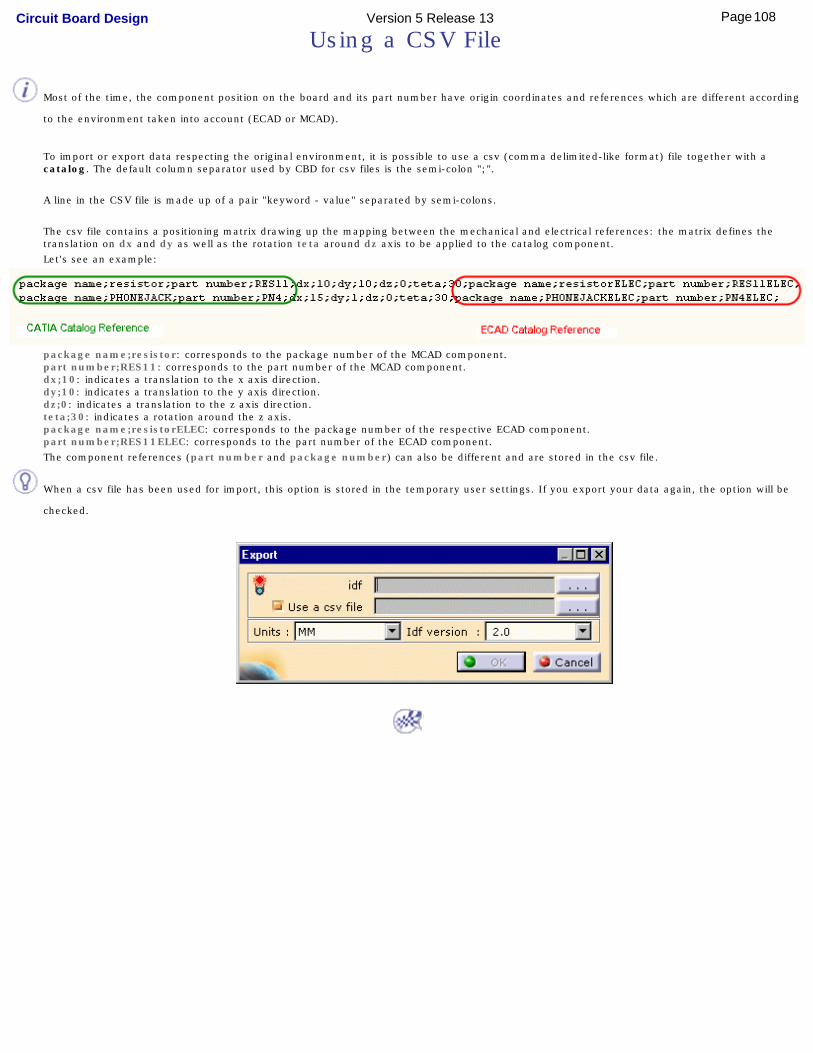
Using a CSV File
Most of the time, the component position on the board and its part number have origin coordinates and references which are different according
to the environment taken into account (ECAD or MCAD).
To import or export data respecting the original environment, it is possible to use a csv (comma delimited-like format) file together with a catalog. The default column separator used by CBD for csv files is the semi-colon ";".
A line in the CSV file is made up of a pair "keyword - value" separated by semi-colons.
The csv file contains a positioning matrix drawing up the mapping between the mechanical and electrical references: the matrix defines the translation on dx and dy as well as the rotation teta around dz axis to be applied to the catalog component.Let's see an example:
package name;resistor: corresponds to the package number of the MCAD component.part number;RES11: corresponds to the part number of the MCAD component.dx;10: indicates a translation to the x axis direction.dy;10: indicates a translation to the y axis direction.dz;0: indicates a translation to the z axis direction.teta;30: indicates a rotation around the z axis.package name;resistorELEC: corresponds to the package number of the respective ECAD component.part number;RES11ELEC: corresponds to the part number of the ECAD component.The component references (part number and package number) can also be different and are stored in the csv file.
When a csv file has been used for import, this option is stored in the temporary user settings. If you export your data again, the option will be
checked.
108Page Circuit Board Design Version 5 Release 13

Workbench Integration
In Assembly context, move the components on the board respecting the constraints.
Launch the DMU Space Analysis to perform a clash check.
109Page Circuit Board Design Version 5 Release 13

Assembly
The integration with the Assembly Design workbench lets you move the components on the board or panel, provided you are allowed to do so by the related constraints in the context of the full digital product definition.
Refer to the Component Management section for more information.
110Page Circuit Board Design Version 5 Release 13
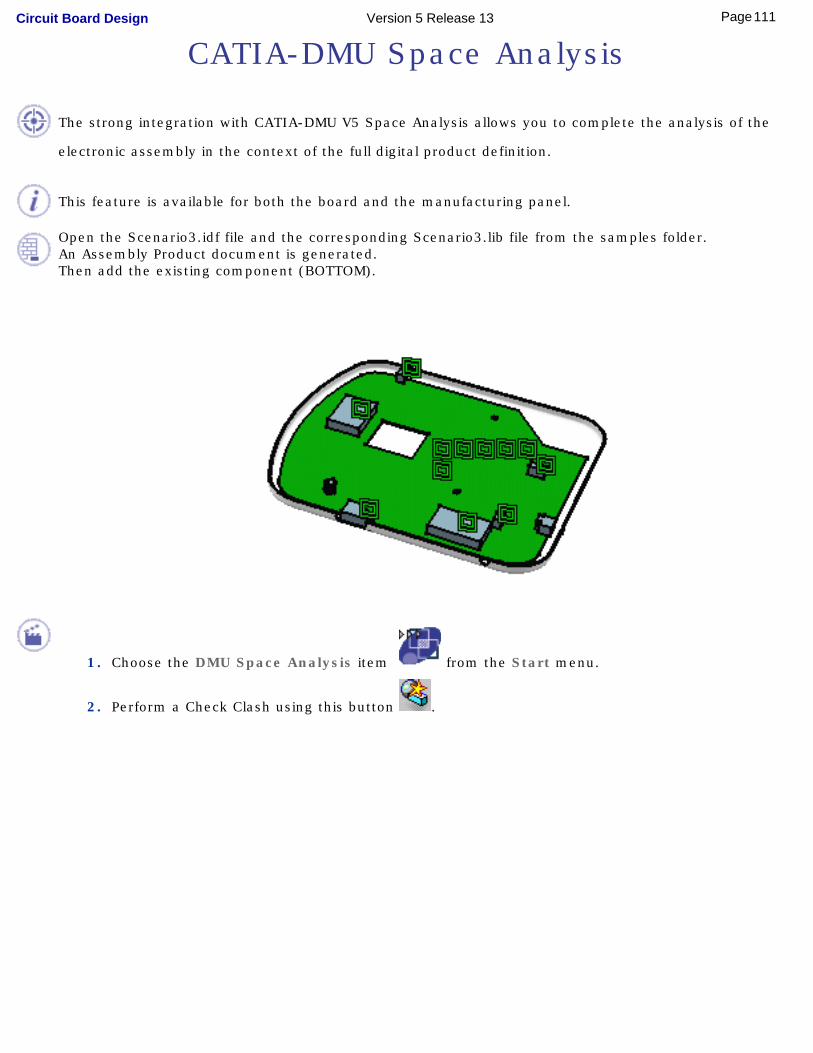
CATIA-DMU Space Analysis
The strong integration with CATIA-DMU V5 Space Analysis allows you to complete the analysis of the
electronic assembly in the context of the full digital product definition.
This feature is available for both the board and the manufacturing panel.
Open the Scenario3.idf file and the corresponding Scenario3.lib file from the samples folder.An Assembly Product document is generated.Then add the existing component (BOTTOM).
1. Choose the DMU Space Analysis item from the Start menu.
2. Perform a Check Clash using this button .
111Page Circuit Board Design Version 5 Release 13

The Preview window shows the clash:
112Page Circuit Board Design Version 5 Release 13

The analysis reveals a clash. You can:
● either change the location of the component respecting the geometrical constraints
● or create a mechanical constraint area taking the clash into account; then transmit the information to the ECAD system in order to integrate it into the placing/routing algorithm.
For more information about DMU Space Analysis capabilities, refer to CATIA-DMU Space
Analysis User's Guide.
113Page Circuit Board Design Version 5 Release 13
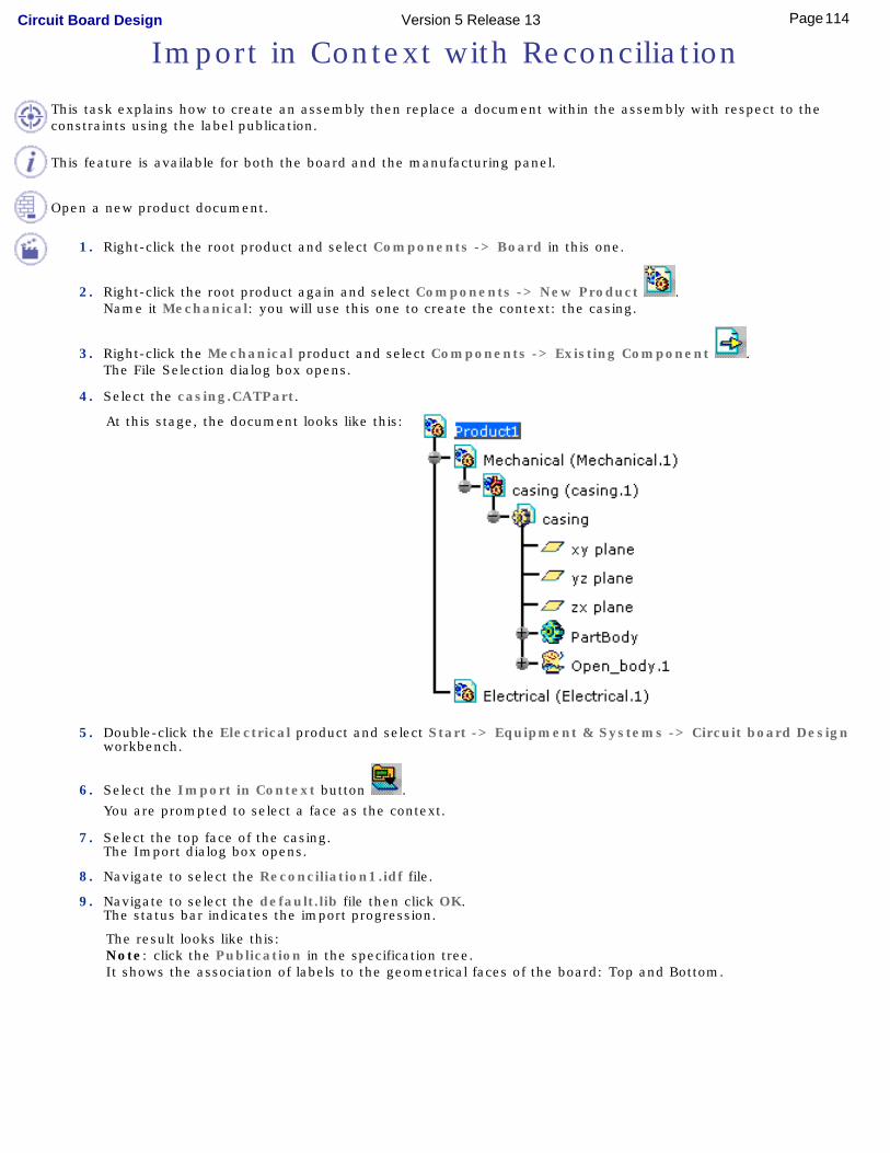
Import in Context with Reconciliation
This task explains how to create an assembly then replace a document within the assembly with respect to the constraints using the label publication.
This feature is available for both the board and the manufacturing panel.
Open a new product document.
1. Right-click the root product and select Components -> Board in this one.
2. Right-click the root product again and select Components -> New Product .Name it Mechanical: you will use this one to create the context: the casing.
3. Right-click the Mechanical product and select Components -> Existing Component .The File Selection dialog box opens.
4. Select the casing.CATPart.
At this stage, the document looks like this:
5. Double-click the Electrical product and select Start -> Equipment & Systems -> Circuit board Design workbench.
6. Select the Import in Context button .You are prompted to select a face as the context.
7. Select the top face of the casing.The Import dialog box opens.
8. Navigate to select the Reconciliation1.idf file.
9. Navigate to select the default.lib file then click OK.The status bar indicates the import progression.
The result looks like this:Note: click the Publication in the specification tree.It shows the association of labels to the geometrical faces of the board: Top and Bottom.
114Page Circuit Board Design Version 5 Release 13
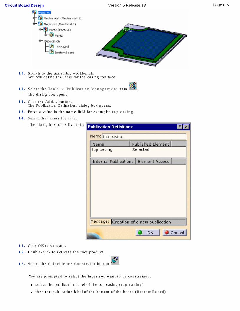
10. Switch to the Assembly workbench.You will define the label for the casing top face.
11. Select the Tools -> Publication Management item .The dialog box opens.
12. Click the Add... button.The Publication Definitions dialog box opens.
13. Enter a value in the name field for example: top casing.
14. Select the casing top face.
The dialog box looks like this:
15. Click OK to validate.
16. Double-click to activate the root product.
17. Select the Coincidence Constraint button .
You are prompted to select the faces you want to be constrained:
■ select the publication label of the top casing (top casing)
■ then the publication label of the bottom of the board (BottomBoard)
115Page Circuit Board Design Version 5 Release 13

The coincidence constraint is created and the Constraint Properties dialog box opens:
It shows the t type, components and status of the constrain.Click OK to validate.
18. Right-click the Electrical Product and select Components -> Replace Component .The File Selection dialog box opens.
19. Select the Reconciliation2.idf file.
In this file a pocket has been added to the board.The Import dialog box opens to let you choose the default.libThe status bar indicates the progression.The result looks like this:
20. Double-click the Constraint button .
You can see the Constraint Definition.The coincidence constraint has been maintained although the board has been replaced.
116Page Circuit Board Design Version 5 Release 13
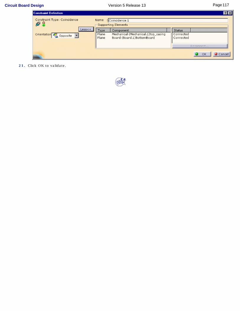
21. Click OK to validate.
117Page Circuit Board Design Version 5 Release 13

Workbench DescriptionThe CATIA - Circuit Board Design Version 5 application window looks like this:
Click the hotspots to display the related documentation.
Menu BarCircuit Board Toolbar
Specification Tree
118Page Circuit Board Design Version 5 Release 13

Menu Bar
The Menu Bar and items which are available in Circuit Board Design workbench are the standard ones. The
different commands and tools are described in Infrastructure Version 5.
For more information, refer to the standard Menu Bar section.
119Page Circuit Board Design Version 5 Release 13

Circuit Board ToolbarThis section describes the various icons available in the Circuit Board Design workbench.The toolbar is located on the right in the default set-up.
See Creating a Board
See Creating a Constraint Area
See Drill Holes After Import
See Creating a Panel
See Exporting Data in an IDF File
See Import in Context
See Sketching a Profile
See Creating a Pad
See Creating a Pocket
See Creating a Hole
See Pattern
See Creating a Component
See Export a Component
120Page Circuit Board Design Version 5 Release 13

Specification TreeWithin the Circuit Board Design workbench, you can generate a number of features that are identified in the specification tree by the following icons.
Manufacturing panel
Board
Component
Label associated to the geometrical face of the board or panel
121Page Circuit Board Design Version 5 Release 13

Customizing Circuit Board Design
This task shows you how to change the user settings. These are permanent settings.
1. Select the Tools -> Options menu.
The Options dialog box opens.
2. Click Equipment & Systems in the left-hand box.
3. Click the Circuit Board Design workbench:
The Circuit Board Design workbench displays with two tabs:
The Graphic tab lets you set the color of your choice to the different areas.If you check the Update documents in session box, your change will be applied to the current document.
122Page Circuit Board Design Version 5 Release 13
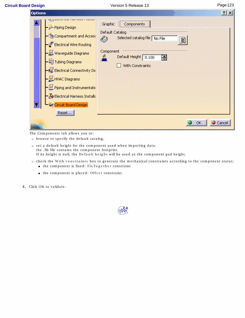
The Components tab allows you to:❍ browse to specify the default catalog,
❍ set a default height for the component used when importing data:the .lib file contains the component footprint.If its height is null, the Default height will be used as the component pad height.
❍ check the With constraints box to generate the mechanical constraints according to the component status:■ the component is fixed: FixTogether constraint
■ the component is placed: Offset constraint.
4. Click OK to validate.
123Page Circuit Board Design Version 5 Release 13

Glossary
Aannotations Allow the electrical and mechanical designers to communicate additional information
about the design. They are not intended to be used for manufacturing purpose.
Bboard A pad with technological propertiesBOTTOM The technological property of a board face which makes it the copper plated face
Ccomponent An electronic part defined in the electronic schematic and stored in the ECAD
component librarycomponent status Describes the position of a component on a board:
unplaced: there is no constraint between the component and the boardplaced: there is a surface contact between the component and the boardfixed: there is a fixity constraint between the component and the boardDedicated geometrical constraints are also associated with components and determine whether you can move them.
constraint area A space reservation used for different purposes such as allowing/forbidding the routing or placing of components etc.When importing an IDF file, each constraint area belongs to a separate body under the PartBody. The separate body is renamed with the constraint area type (ex: PLACE_KEEPOUT).This feature is available on both the board and the manufacturing panel.
cutout A hole or a pocket on a board
Ddrilled hole A hole used to mount a board in its case
E
ECAD Electrical Computer Aided Design
Ffixed See component status
IIDF Intermediate Data Format
124Page Circuit Board Design Version 5 Release 13

MMCAD Mechanical Computer Aided Designmulti-domain(constraint area)
A multi-domain constraint area is a space reservation made up of several elements in the same body. Each multi-domain constraint area belongs to a separate body under the PartBody.This feature is available on both the board and manufacturing panel.
N
NPTH Non plated: technological property of a hole which is not conductive (mounting hole)
Ooffset Represents the mounting constraint of a component onto the board. It can also be
found between the board and the panel.other outline Other area type defined by an outline, cutouts and a thickness
Ppanel Optional file added to IDF 3.0 standard to allow manufacturing information
exchange. It contains the manufacturing panel physical description as well as the boards and components location on the panel.
placed See component statusplace keepout A mechanical space reservation where the component height is limitedplace outline An area where component placing is allowedplace region An area where placing is limited to component of certain typesPTH Plated: technological property of a hole which is conductive
Rroute keepout An area where routing electrical connections is forbiddenroute outline An area where routing electrical connections is allowed
Sstatus See component status
TTOP The technological property of a board face which means it is not the copper plated
face
Uunplaced See component status
125Page Circuit Board Design Version 5 Release 13

Vvia keepout An area where placing via is forbidden
126Page Circuit Board Design Version 5 Release 13

Index
Aannotation
Bboard BOTH
constraint area BOTTOM
constraint area
Ccatalog command
Check Clash
Coincidence Constraint
Constraint Area
Create a Component
Create Board
Create Constraint Area
Edit Links
Exit Sketcher
Export
Export a Component
Hole
Import in Context
Manipulation
127Page Circuit Board Design Version 5 Release 13

Pad
Panel
Profile
Rectangular Pattern
Sketcher
Update component
properties
component status constraint area
BOTH
BOTTOM
creating interactively
defining
definition
multi-domain
properties
TOP csv file
mapping table
cutout
EECAD
Ffixed
128Page Circuit Board Design Version 5 Release 13
Hhole
automatic recognition
creating
IIDF
IDF 3.0
Mmapping table
csv file
mechanical constraint
multi-domain
constraint area multi-domain constraint area
definition
NNPTH
Ooffset
Other outline
129Page Circuit Board Design Version 5 Release 13
Ppanel
patterns of pattern
Place keepout
place keepout
Place outline
Place region
placed
pocket and holes
properties properties
component
constraint area
pocket and holes
PTH
RRoute keepout
Route outline
Ttechnological property TOP
constraint area
Uunplaced
130Page Circuit Board Design Version 5 Release 13

VVia keepout
131Page Circuit Board Design Version 5 Release 13