CHARGE-BASED COMPACT MODEL OF GATE-ALL-AROUND...
79
CHARGE-BASED COMPACT MODEL OF GATE-ALL-AROUND FLOATING GATE NANOWIRE WITH VARIABLE OXIDE THICKNESS FOR FLASH MEMORY CELL MUHAMMAD AFIQ NURUDIN BIN HAMZAH UNIVERSITI TEKNOLOGI MALAYSIA
Transcript of CHARGE-BASED COMPACT MODEL OF GATE-ALL-AROUND...
CHARGE-BASED COMPACT MODEL OF GATE-ALL-AROUND FLOATINGGATE NANOWIRE WITH VARIABLE OXIDE THICKNESS FOR FLASH
MEMORY CELL
MUHAMMAD AFIQ NURUDIN BIN HAMZAH
UNIVERSITI TEKNOLOGI MALAYSIA

CHARGE-BASED COMPACT MODEL OF GATE-ALL-AROUND FLOATINGGATE NANOWIRE WITH VARIABLE OXIDE THICKNESS FOR FLASH
MEMORY CELL
MUHAMMAD AFIQ NURUDIN BIN HAMZAH
A thesis submitted in fulfilment of therequirements for the award of the degree of
Doctor of Philosophy
Faculty of Electrical EngineeringUniversiti Teknologi Malaysia
JUNE 2018

iii
To my beloved family and friends.

iv
ACKNOWLEDGEMENT
I would like to express my deepest appreciation to whom I owe a debt incompleting this Phd work.
First, I would like to express my very great appreciation to my supervisor,Professor Dr. Razali Bin Ismail for such valuable advice and wonderful mentoring.Through his experience in man-management and enthusiasm, he paved the path for mein becoming a well-around academician and researcher. He tirelessly giving valuableadvice and encouragement to become success in academia by rapidly and continuallyto publish academic work. He always quoted “publish or perish” has been a taboo andbenchmark for me in pursuing success.
Secondly, I also thank to my co-supervisor, Dr. Nurul Ezaila Bt. Alias for allthe technical support and advice that inevitably improved the quality of my work. Herendearing supervision has made me even more motivated in delivering positive andquality output for my research work.
My companions in the Computational Nanoelectronic Research lab for all thesupport in variety of ways. Special thanks to Lim Wei Hong, Fatimah Khairiah andSakinah for sharing their ideas and giving significant contribution in improving myworks. Not to forget Mr. Zulkifli, Maryati Morsin, Adila Syaidatul, Zuriana and WeiHow for their support.
Million thanks to my family, especially to my parents, for all theirunderstandings and emotional supports for giving me the encouragement to go forth inmy career and life.
I would like to thank the Universiti Teknologi Malaysia (UTM) for the ZamalahScholarship and it has been a privilege staying here. Last but not least, to the Ministryof Science, Technology and Industry (MOSTI) for providing funds for conferencetravels and publication charges.

v
ABSTRACT
Due to high gate electrostatic control and introduction of punch and plug
process technology, the gate-all-around (GAA) transistor is very promising in, andapparently has been utilized for, flash memory applications. However, GAA FloatingGate (GAA-FG) memory cell still requires high programming voltage that may besusceptible to cell-to-cell interference. Scaling down the tunnel oxide can reducethe Program/Erase (P/E) voltage but degrades the data retention capability. Byusing Technology-Computer-Aided-Design (TCAD) tools, the concept of tunnelbarrier engineering using Variable Oxide Thickness (VARIOT) of low-k/high-kstack is utilized in compensating the trade-off between P/E operation and retentioncharacteristics. Four high-k dielectrics (Si3N4, Al2O3, HfO2 and ZrO2) that arecommonly used in semiconductor process technology are examined with SiO2 asits low-k dielectric. It is found that by using SiO2/Al2O3 as the tunnel layer, boththe P/E and retention characteristics of GAA-FG can be compensated. About 30%improvement in memory window than conventional SiO2 is obtained and only 1%of charge-loss is predicted after 10 years of applying gate stress of -3.6V. Compactmodel of GAA-FG is initiated by developing a continuous explicit core model ofGAA transistor (GAA Nanowire MOSFET (GAANWFET) and Juntionless NanowireTransitor (JNT)). The validity of the theory and compact model is identified based onsophisticated numerical TCAD simulator for under 10% maximum error of surfacepotential. It is revealed that with the inclusion of partial-depletion conduction, theaccuracy of the core model for GAANWFET is improved by more than 50% inthe subthreshold region with doping-geometry ratio can be as high as about 0.86.As for JNT, despite the model being accurate for doping-geometry ratio upto 0.6,it is also independent of fitting parameters that may vary under different terminalbiases or doping-geometry cases. The compact model of GAA-FG is completed byincorperating Charge Balance Model (CBM) into GAA transistor core model wheregood agreement is obtained with TCAD simulation and published experimental work.The CBM gives better accuracy than the conventional capacitive coupling approachunder subthreshold region with approximately 10% error of floating gate potential.Therefore, the proposed compact model can be used to assist experimental work inextracting experimental data.
vi
ABSTRAK
Oleh kerana kawalan elektrostatik get yang tinggi dan pengenalan kepadateknologi proses tebuk dan plak, transistor get-silinder-menyeluruh (GAA) sangatmeyakinkan, dan telah digunakan dalam aplikasi memori flash. Walaubagaimanapun,GAA get terapung (GAA-FG) masih memerlukan voltan program yang tinggi yangmungkin terdedah kepada gangguan cell-to-cell. Pengecilan-skala terowong oksidadapat mengurangkan voltan program/padam (P/E) tetapi menyebabkan kemerosotankepada daya-pengekalan datanya. Dengan menggunakan perisian rekabentuk-berbantukan-teknologi-komputer (TCAD), konsep Kejuruteraan Terowong Pengha-dang Oksida Boleh-ubah (VARIOT) k-rendah/k-tinggi telah digunakan dalam konteksmengimbangi kurang-lebih antara operasi program/padam dan daya-pengekalan data.Empat dielektrik k-tinggi (Si3N4, Al2O3, HfO2, ZrO2) yang kebiasaannya terdapatdalam industri semikonduktor dianalisa dengan SiO2 sebagai dielektrik k-rendah.Hasil simulasi menunjukkan gabungan SiO2/Al2O3 sebagai lapisan terowong GAA-FG dapat mengimbangi kurang-lebih antara operasi program/padam dan daya-pengekalan data. Sebanyak 30% peningkatan jendela memori berbanding SiO2
dan hanya 1% kehilangan cas dijangkakan selapas 10 tahun dikenakan voltan-getsetinggi -3.6V. Model kompak bagi GAA-FG dimulai dengan penghasilan modeleksplisit berterusan untuk transistor GAA (GAANWFET dan JNT). Kesahihanantara teori dan model kompak dipastikan berdasarkan perisian simulasi TCADbagi ralat maksimum beza-upaya permukaan sebanyak 10%. Hasil menunjukkan,dengan mengambil kira kesan konduksi separa-habis dapat meningkatkan ketepatanmodel-teras GAANWFET sebanyak lebih daripada 50% dalam kawasan sub-ambanguntuk nisbah dopan-geometri sehingga 0.86. Bagi JNT pula, disamping modelkompaknya tepat untuk nisbah dopan-geometri sehingga 0.6, ia juga tidak bergantungkepada parameter-cubaan yang mungkin berubah-ubah bagi voltan-terminal ataunisbah dopan-geometri yang berbeza. Model kompak GAA-FG disempurnakan hasilgabungan model pengimbang-cas (CBM) dan model kompak transistor GAA yangmana ketepatannya teruji baik dengan simulasi TCAD dan hasil eksperimen yangsudah diterbit. CBM memberikan ketepatan yang lebih baik berbanding kaedahkapasitif-gandingan konvensional pada bahagian sub-ambang dengan ralat beza-upaya get-terapung sebanyak 10%. Oleh itu, model kompak yang dihasilkan dapatdigunaakan untuk membantu kerja-kerja eksperimen bagi mengekstrak nilai parameter.
vii
TABLE OF CONTENTS
CHAPTER TITLE PAGE
DECLARATION iiDEDICATION iiiACKNOWLEDGEMENT ivABSTRACT vABSTRAK viTABLE OF CONTENTS viiLIST OF TABLES xiLIST OF FIGURES xiiLIST OF ABBREVIATIONS xxiiLIST OF SYMBOLS xxvLIST OF APPENDICES xxviii
1 INTRODUCTION 11.1 Research Background 11.2 Flash Memory Scaling Challenges and Motivation 31.3 Problem Statements 81.4 Research Objectives 111.5 Research Scopes 121.6 Research Contribution 121.7 Thesis Organization 13
2 LITERATURE REVIEW 152.1 Introduction 152.2 Gate-All-Around Floating Gate (GAA-FG) Structu-
res 152.2.1 Planar GAA-FG Cell 162.2.2 Vertical Channel GAA-FG cell 18

viii
2.2.2.1 Conventional-FloatingGate/Stacked-SurroundingGate Transistor (C-FG/S-SGT) 18
2.2.2.2 Dual Control Gate-SurroundingFloating Gate (DC-SF) 19
2.2.2.3 Separated-Sidewall ControlGate (S-SCG) 20
2.2.2.4 Sidewall Control Pillar (SCP) 222.3 Barrier Engineering Concept 23
2.3.1 Crested Barrier 242.3.2 VARIable Oxide Thickness (VARIOT) 272.3.3 Crested Barrier versus VARIOT 30
2.4 Device Modeling 312.4.1 Overview of GAANWFET Core Models 352.4.2 Overview of Junctionless Nanowire Tran-
sistor (JNT) Core Models 442.4.3 Explicit Solution to Core Model 512.4.4 Floating Gate Potential Models 57
2.5 Summary 63
3 RESEARCH METHODOLOGY 643.1 Introduction 643.2 Research Activities 653.3 Device Optimization and Characterization Appro-
ach 673.4 Device Compact Modeling Approach 713.5 Summary 73
4 GAA-FG WITH VARIOT TUNNEL LAYER DESIGN 754.1 Introduction 754.2 Parameter Optimization of Asymmetric VARIOT 754.3 GAA-FG Simulation 83
4.3.1 Validation Work of GAA-FG MemoryCell 83
4.3.2 Device Performances of GAA-FG CellIncorporating VARIOT Tunnel Layer 91
4.4 Summary 96

ix
5 CHARGE-BASED COMPACT MODELING OF GAA-FG 985.1 Introduction 985.2 Charge-Based Compact Model of GAANWFET 99
5.2.1 Implicit Continuous Charge-Based Model 1005.2.2 Explicit Solution of Unified Charge
Control Model (UCCM) 1045.2.3 Current-Voltage (I-V), Charge-Voltage
(Q-V) and Capacitance-Voltage (C-V)Characteristics 109
5.2.4 Partial-Depletion Conduction of GAAN-WFET 116
5.3 Charge-Based Compact Model of JunctionlessNanowire Transistor (JNT) 1245.3.1 Implicit Continuous Charge-Based Model 1255.3.2 Explicit Solution of Unified Charge
Control Model (UCCM) 1295.3.3 Current-Voltage (I-V), Charge-Voltage
(Q-V) and Capacitance-Voltage (C-V)Characteristics 133
5.4 Floating Gate Potential Model of GAA-FG MemoryCell 141
5.5 Summary 147
6 CONCLUSION AND RECOMMENDATION 1496.1 Introduction 1496.2 Summary and Conclusion 149
6.2.1 TCAD simulation on optimization ofVARIOT tunnel layer 149
6.2.2 TCAD simulation on GAA-FG perfor-mances using VARIOT tunnel layer 150
6.2.3 Charge-based compact model of GAAN-WFET 150
6.2.4 Charge-based compact model of JNT 1516.2.5 Charge-based compact model GAA-FG
memory cell 1526.3 Future Works 153

x
REFERENCES 157Appendices A – C 172 – 192

xi
LIST OF TABLES
TABLE NO. TITLE PAGE
2.1 Common MOSFET models available in circuit simulators. 322.2 GAANWFET core models. 432.3 Development of JNT core models. 503.1 Flash memory operational constraints. 694.1 Parameters for different dielectric materials used in simula-
tion. 764.2 Optimized parameters and extracted F-N coefficients for
device characterization purpose. 824.3 Parameters used in simulation work and experimental GAA-
FG cell in Lee et al., (2013). 854.4 VARIOT physical thickness and EOT used in simulation. 91A.1 Parameters and data for SiO2/Si3N4 extracted from TCAD
simulation. 172A.2 Parameters and data for SiO2/Al2O3 extracted from TCAD
simulation. 174A.3 Parameters and data for SiO2/HfO2 extracted from TCAD
simulation. 176A.4 Parameters and data for SiO2/ZrO2 extracted from TCAD
simulation. 178

xii
LIST OF FIGURES
FIGURE NO. TITLE PAGE
1.1 The memory device based on Complementary Metal-Oxide-Semiconductor (CMOS) technology divided into twocategories, which are volatile and non-volatile. 1
1.2 (a) Number of storage capacity exponentially increasethroughout the years with storage application devices isthe highest. (Source from Forward Insight). (b) Memoryrevenue on some of the companies manufacturing variousmemory devices and the top five companies consolidationin memory industry, majorly dominated by companies thatsold flash memory (source from Micron 2014 Winter AnalystConference). 3
1.3 Summarized the downscaling issues in term of performancerelated to the gate stack of the conventional wraparound FGcell in NAND flash memory. 4
1.4 Scaling limitation of 2-D NAND flash. (a) Increments incell-to-cell interference of a victim cell across BL, WL anddiagonal FGs and (b) decrements in number of electron infloating gate. 5
1.5 Roadmap from top semiconductor foundries for scaling 2-Dand 3-D NAND flash architectures (source from ICinsight,2014). 6
1.6 (a) Comparison of relative bit cost of 3-D architecture NANDflash between the stacking of conventional 2-D planar NANDand Bit-Cost Scalable (BiCS) NAND technology as thenumber of layer increases. (b) BiCS fabrication method. 7
1.7 (a) Comparison of threshold voltage shift after program withcontrol gate voltage (Vcg) and after bulk erase between C-FG,S-SCG and SCP 3-D NAND cells. (b) Trade-off between P/Escalability and retention characteristics for differents tunneloxide thickness. 9

xiii
2.1 (a) Fabrication steps for GAA-FG memory cell and (b) thecross-section of the device consists of control gate (CG),floating gate (FG), SiO2 tunnel oxide, SiO2 IPD layer andpoly-Si channel. 16
2.2 Electric field of (a) GAA-SONOS charge trapping and (b)GAA-FG during program at 10-6 and 10-3 s. 17
2.3 (a) Fabrication process steps for IMFT 3-D NAND flash C-FG memory cell and (b) the cross-section of its memory cellconsists of control gate (CG), floating gate (FG), IPD oxidelayer, tunnel oxide and poly-Si channel. 19
2.4 (a) Fabrication process steps for SK Hynix 3-D NAND flashDC-SF memory cell and (b) the cross-section of the memorycell showing the poly-Si floating gate (FG) and its two poly-Sicontrol gates (CGs) with IPD oxide layer separating betweenthem. 20
2.5 (a) Fabrication process steps for SK Hynix 3-D NAND flashwith S-SCG memory cell and (b) the cross-section of thememory cell showing the two SCGs act as electrical S/Dlayer. 21
2.6 (a) Fabrication process steps for SK Hynix 3-D NAND flashwith SCP memory cell and (b) the cross-section of thememory cell showing the poly-Si pillar and its dimension oflength, Lscp and width, Wscp. 22
2.7 Shows the conduction band diagram of (a) typical uniformheight barrier, (b) and (c) are the ideal form of symmetricand asymmetric crested barrier respectively. (d) and (e) arethe actual form of symmetric and asymmetric crested barrierrespectively. Parameter e, V , U , U ′, d and d′ are the electroncharge, applied bias, low-k energy barrier, high-k energybarrier, low-k layer thickness, and high-k layer thickness. 24
2.8 Conduction band diagram between (a) typical uniformbarrier, (b) symmetric crested barrier and (c) asymmetriccrested barrier during retention (no applied bias V ) and afterapplied bias V . U is the low-k barrier height and U ′ is thehigh-k barrier height. 25
2.9 The current density (dashed lines) and the gate rechargingtime (lines) of the crested barriers and single-layer barrierwith various physical thickness. The notations of the plot (a)-(e) are in accordance to Figure 2.7. 26

xiv
2.10 Comparison of JG against applied bias for crested and single-layer barriers with same EOT of 5nm. Y3O2, Si3N4 and ZrO2
have been used as the outer layer of crested barriers beingAl2O3 and SiO2 as the middle layer. 27
2.11 Schematic shows the stacking of (a) symmetric VARIOT and(b) asymmetric VARIOT with their respective band diagramat flat-band condition. 28
2.12 Comparison of the conduction band diagram for (a)asymmetric and (b) symmetric VARIOT structures with thesingle-layer SiO2 barrier during retention and applied bias V . 28
2.13 (a) Comparison of JG − V characteristics between VARIOTand single layer SiO2. (b) Summarizes the advantages ofVARIOT (straight line) having steeper slope than SiO2 (dottedline) for EOT=5nm. 29
2.14 Comparison of (a) JG − VFG characteristics for variouscombinations of crested barrier and VARIOT with EOT=5nm.(b) Sketch of the conduction band diagram of symmetricVARIOT showing electron injection in both elastic andineleastic limits. 31
2.15 Definition of compact modeling with its analytical approa-ches and solution. 34
2.16 Schematic cross-section of GAANWFET and its relatedvariables. 36
2.17 Comparison of drain current between model and TCADsimulation (Circles) for R = 10nm from intrinsic to highbody concentration upto 1× 1019cm-3. 40
2.18 (a) Normalized potential for intrinsic to body concentrationof 3 × 1018cm-3. (b) Comparison of drain current betweenmodel in Zhang et. al., (2009) (Red lines) and Liu et. al.,
(2008) (Black lines) with TCAD simulation (Squares) forR = 10nm. 42
2.19 Comparison of schematic structure between JNT device tothe conventional inversion-mode (IM) transistor. JNT hasidentical dopant concentration in the body to that of the S/Dregions (n+/n+/n+). 44
2.20 Transfer characteristics and its operation regimes of (a)Junctionless Nanowire Transistor and (b) conventionalinversion-mode GAANWFET. 45
xv
2.21 Comparison of CV characteristics at gate terminal betweencompact model developed by Oana et al., (2014) withTCAD Atlas simulation results for (a) various high-dopantconcentration and (b) small-radii. 49
2.22 Schematic of CCCM floatimg gate cell, where Ccg, Cox, Cd,and Cs are the capacitances between FG and CG, channel,drain and source respectively. 58
2.23 I-V curves of reference (R) and floating gate devices (F) forVd = 0.1V (R1 and F1) and Vd = 0.6V (R2 and F2). S is thesubthreshold slope of the FG cell and S0 is the subthresholdslope of the reference cell. 60
2.24 Schematic of CBM FG memory cell, consists of controlgate capacitance Ccg, MOS transistor equivalent to thememory cell, and voltage-controlled voltage source (VCVS)of floating gate, Vfg. 61
3.1 Research methodology flowchart of GAA-FG memory cellwith VARIOT tunnel layer and GAA devices compactmodeling. 66
3.2 Flowchart for device simulation work. 673.3 Parameters involved in simulation of GAA-FG cell using
asymmetric VARIOT tunnel oxide with its comparative study. 713.4 Flowchart for device modeling work. 724.1 Metal-Oxide-Semiconductor (MOS) capacitor structure with
low-k/high-k stack as its gate oxide. 764.2 JV characteristics of SiO2/Si3N4 for EOT=4nm. The
horizontal dashed-lines are the imposed constraints duringprogram, read-disturb and retention. The red dashed-lines justto show the boundaries of electron tunneling mechanism forTox=3nm depending of Vtr and Vfn. 77
4.3 Vg − Tox plot of program constraint for (a) SiO2/Si3N4 (b)SiO2/Al2O3 (c) SiO2/HfO2 and (d) SiO2/ZrO2. 79
4.4 Vg − Tox plot of read-disturb and retention constraints for (a)SiO2/Si3N4 (b) SiO2/Al2O3 (c) SiO2/HfO2 and (d) SiO2/ZrO2.The upper plot (Vg > 0) is after imposing the read-disturbconstraint at Jg = 7 × 10⁻¹¹A/cm2 and the lower plot(Vg ≤ 0) is after imposing the retention constraint at Jg =
2 × 10⁻¹⁶A/cm2. The symbols are consistent with legend inFigure 4.3. 80
xvi
4.5 Optimized gate voltage for each EOT of all asymmetricVARIOTs due to (a) retention constraint of >|-1.5V| and (b) amore restrictive read-disturb constraint of >3.6V. 81
4.6 (a) The cross-section of experimental GAA-FG withtriangular nanowire. (b) The cross-section of GAA-FGstructure showing silicon nanowire channel and source/drainregion with its electrode, and poly-Si FG being surrounded bySiO2. 84
4.7 Comparison of transfer characteristics between 3-D simula-tion with experimental data by Lee et al., (2013) for drain biasof 0.1V and 1.0V. Device simulation with (line) and without(dashed-line) definition of interface traps near the conductionare also shown. 86
4.8 Comparison of P/E characteristics between simulation andexperimental data in Lee et al., (2013) for a given P/Evoltages of 10/-8V up to 10ms. P/E characteristics of GAA-FG cell with Tox scaling limit of 6nm SiO2 to indicate fastcharging. 87
4.9 Electric field distribution along the radial direction of GAA-FG cell in (a) simulation and (b) extracted experimental resultin Lee et al., (2013). 88
4.10 Comparison of retention characteristics between GAA-FGcell of 8nm and 11nm SiO2 with experimental data (black)in Lee et al., (2013) after a P/E cycle for P/E voltages of10/-8V and P/E time of 5/2ms. The lines are the 10 yearsextrapolation results of threshold voltage using Power’s law. 90
4.11 (a) Fabrication process of C-FG cell with an additionaldeposition of high-k dielectric before low-k and poly-Sichannel were form. (b) Schematic diagram of GAA-FG cellwith asymmetric VARIOT as tunnel oxide layer. Tox and THare the thickness for low-k and high-k dielectric materials. 91
4.12 JV characteristics for various low-k/high-k tunnel layer. Allstacks have physical thickness of 11nm. The 6nm and 8nmSiO2 layer are the control device to indicate high programcurrent and retention characteristics. Steeper slope and gatecurrent density are achieved with decreasing of EOT. 92

xvii
4.13 (a) C-V curves for various low-k/high-k tunnel layer. (b)Electric field profile of GAA-FG cells across the gate stack.SiO2/Al2O3 stack yield the utmost surface field at Si/SiO2
interface. 934.14 Comparison of P/E characteristics of GAA-FG cell using
VARIOT tunnel layer with GAA-FG of 6nm SiO2. indicatesfaster P/E operation but higher voltage is required for eraseoperation. 94
4.15 Retention characteristics of GAA-FG with VARIOT tunnellayer of (a) SiO2/Si3N4 (b) SiO2/Al2O3, (c) SiO2/HfO2 and (d)SiO2/ZrO2 under gate stress of -3.6/3.6V. Data retention forGAA-FG of 8nm SiO2 is plotted to benchmark 20% charge-loss under similar gate stress. 96
4.16 Performance comparison of GAA-FG incorporating VARIOTtunnel layer with experimental results in Lee et al., (2013). 97
5.1 Schematic diagram for n-channel GAANWFETs withcylindrical coordinate system. The diagram also shows thedistribution of interface trap densities, Dit and fixed oxidecharges, Qf . 100
5.2 Comparison of mobile charge density between explicitexpression of Equation (5.16) with iterative/implicit solutionof Equation (5.13). 105
5.3 Comparison of Qm against Vg curves at Vd = 0V betweenexplicit model (5.19) and implicit model from intrinsic (NA =
1.45 × 1010cm-3) to higher doping concentration of 1 ×1019cm-3. 107
5.4 Comparison of Qm against Vg curves at Vd = 0V betweenexplicit model (5.19) and implicit UCCM for a wide range ofR in (a) intrinsic and (b) higher doping concentration (NA =
1× 1019cm-3). 1075.5 Comparison of Qm against Vg curves at Vd = 0.05V, between
explicit model (5.19) and implicit UCCM for various range ofQf in (a) intrinsic and (b) higher doping concentration (NA =
1× 1019cm-3). 1085.6 Comparison of Qm against Vg curves at Vd = 0.05V, between
explicit model (5.19) and implicit UCCM for various range ofDit in (a) intrinsic and (b) higher doping concentration (NA =
1× 1019cm-3). 108
xviii
5.7 Assuming zero trap state density (Qf = 0, and η = 1), (a)shows the Ids − Vg curves of GAANWFET from intrinsic tohigh doping concentration and (b) the Ids − Vd curves withwide range of operating gate voltage are verified with 3Ddevice simulation. 110
5.8 Given Qm from (5.19), comparison of Ids − Vg for (a)fixed oxide charges and (b) interface trap densities againstnumerical simulation are in good agreement. 110
5.9 Comparison between explicit models in Cheralathan et al.,(2011) and (5.19) with implicit UCCM solution for NA = 1 ×1017cm-3 and NA = 1 × 1019cm-3. (a) Shows the Qm against Vgcurves and (b) Ids against Vg at Vd = 1.0V. 111
5.10 Comparison between analytical model with numerical TCADsimulation of (a) normalized transconductance and (b)conductance for Vd=0.05V and 1.0V. Terminal charges ofGAANWFET (c) against Vg and (d) against Vd for NA =
3× 1018cm-3. The parameters are consistent for all figures. 1135.11 Comparison of intrinsic capacitances across (a)-(c) gate
voltage and (b) drain voltage between analytical models withnumerical TCAD simulation results for heavily doped bodyof NA=3×1018 cm-3. Analytical models fairly predict thetransition region for a given accurate explicit solution of themobile charge expression. Symbols are consistent for bothplots. 115
5.12 Surface potential due to dopant carrier in partial-depletionconduction of Equation (5.36) and full-depletion conductionof Equation (5.37) for (a) FD-GAANWFET and (b) PD-GAANWFET. The partial-depletion conduction is shown tobe affected by (c) dopant concentration and (d) radius. 118
5.13 Surface and center potentials of GAANWFET withNA=1×1019cm-3 computed using unified function of N
for (a) N=4 and (b) N=12. Optimum value of N is obtainedby comparing with TCAD simulation. 120
5.14 Optimum value of N extracted by comparison with TCADsimulation. The proposed model for N (red-line) fit wellwith extracted data (dot-symbol). Inset shows the error ofanalytical model with referenced to TCAD simulation resultsfor varying qNAR
2/4εSi ratio. 120

xix
5.15 Surface potential model with and without the inclusion ofpartial-depletion conduction compared to TCAD simulationfor (a) different dopant concentration and (b) its percentageerror; for (c) different radii and (d) its percentage error. 121
5.16 Comparison of (a) mobile charge density and (b) transfercharacteristics for various dopant concentration. 122
5.17 Transfer characteristics with various radii for dopant con-centration of (a) NA=1×1016cm-3 and (b) NA=1×1018cm-3.Output characteristics for dopant concentration of (c)NA=1×1016cm-3 and (d) NA=1×1018cm-3 respectively. 123
5.18 Schematic diagram for JNT with cylindrical coordinate system. The
diagram also shows the interface trap densities, Dit and the fixed
oxide charges, Qf are assume to be uniformly distributed along the
channel. 1255.19 Assessment of UCCM model for all operating regions of JNT
at Vd = Vs = 0V . The red vertical lines denote the thresholdand flat-band voltages to indicate the boudaries of operatingregion from full-depletion (FD), partial-depletion (PD) andaccumulation (ACC). 129
5.20 Mobile charge density for depletion (QDP ) and comple-mentary (QC) parts at Vd=0V. The total mobile charge Qm
agreed well with numerical simulation by making QC ascomplementary charge to QDP . 131
5.21 (a) Comparison of surface potential computed usinganalytical model with referenced to TCAD simulation and (b)its error. 132
5.22 Comparison of mobile charge density between proposedmodel with Duarte et al., (2012) that was solved usingiterative method for various (a) dopant concentration and (b)radius. 133
5.23 Transfer characteristics of JNT for various (a) high dopantconcentration and (b) radius compared to numerical TCADsimulation. 135
5.24 Output characteristics for R=10nm at dopant concentration of(a) ND=5×1018cm-3 and (b) ND=1×1019cm-3. 136
5.25 Comparison of (a) transconductance, (b) conductance andterminal charges against (c) gate voltage and (d) drain voltage. 139

xx
5.26 Comparison of all the capacitances (i.e.:- self-capacitancesand transcapacitances) across (a)-(c) gate voltage and (d)drain voltage between analytical models with numericalTCAD simulation results for dopant concentration ofND=1×1019 cm-3. Analytical models fairly predict the partialdepletion region. Symbol and parameter are consistent for allplots. 140
5.27 Cross-section of a symmetrical GAA-FG. R is the radius,Lg is the gate length while Tox and TIPD are the tunneloxide and IPD oxide thicknesses respectively. Ccg is the FG-CG capacitance, Cox is the tunnel oxide capacitance and theintrinsic capacitances with respect to floating gate terminalare denoted as Cgd and Cgs. The channel charge, Qch isequal to the total charge across the gate stack that sum asQfg + Ccg (Vcg − Vfg). 142
5.28 Floating gate potential for various (a) drain voltage and(b) predefined Qfg. For CCCM, fixed capacitive ratios ofαcg=0.64 and αd=0.18 are re-used from CBM to fit withTCAD simulation as well as total capacitance given asCtot=Ccg+Cox+Cd+Cs, with Cd and Cs are extracted fromTCAD simulation as 0.038fF and 0.12fF respectively. 143
5.29 Transfer characteristics of GAA-FG for various (a) drainvoltage and (b) predefined Qfg. 143
5.30 (a) Comparison of proposed model with experimental data.All parameters remain the same as in Table 4.2 except forQf and interface traps parameter η that are treated as fittingparameter. (b) Comparison of floating gate potential betweenproposed model and CCCM approach with referenced toTCAD simulation. Fixed capacitive ratio of αcg=0.73 andαd=0.14 from CBM is re-used in CCCM approach. 145
5.31 (a) Control gate coupling (αcg) and (b) drain coupling (αd)ratios of GAA-FG for Qfg=0 and varying Vcg and Vd usingVfg calculated from the charge balance model. 146
5.32 Comparison of GCR at Vd=0V for VARIOT tunnel layer withreferenced to conventional 11nm SiO2 tunnel layer of GAA-FG fabricated in Lee et al., (2013). 147

xxi
6.1 An array of 3-D FG-NAND that consists of four FG celland two select transistors. Capacitances show the couplingbetween selected FG cell with neigbouring-FG (NFG),control gate and neighbouring control gate (NCG). 154
6.2 (a) Block diagram of read path-circuit and its (b) senseamplifier. 156
A.1 Jg − Vg characteristics of SiO2/Si3N4 for EOT (a) 4nm (b)5nm (c) 6nm (d) 7nm and (e) 8nm. 173
A.2 Jg − Vg characteristics of SiO2/Al2O3 for EOT (a) 4nm (b)5nm (c) 6nm (d) 7nm and (e) 8nm. 175
A.3 Jg−Vg characteristics of SiO2/HfO2 for EOT (a) 4nm (b) 5nm(c) 6nm (d) 7nm and (e) 8nm. 177
A.4 Jg−Vg characteristics of SiO2/ZrO2 for EOT (a) 4nm (b) 5nm(c) 6nm (d) 7nm and (e) 8nm. 179
A.5 (a) JV characteristics for the optimized parameters of allasymmetric VARIOTs conducted. F-N plot of all asymmetricVARIOTs conducted for (b) programming and (c) eraseoperations. 180

xxii
LIST OF ABBREVIATIONS
ACM - Adcanced Compact MOSFET
ALCVD - Atomic Layer Chemical Vapor Deposition
AT - Above Threshold
BiCS - Bit-Cost Scalable
BIOS - Basic Input Output Storage
BT - Below Threshold
BSIM - Berkeley Short-Channel IGFET Model
CBM - Charge Balance Model
CCCM - Capacitive Coupling Coefficient Model
C-FG - Conventional-Floating Gate
CD-ROM - Compact-Disk Read-Only-Memory
CLM - Channel Length Modulation
CMOS - Complementary Metal-Oxide-Semiconductor
CT - Charge Trapping
CTCI - Cell-to-Cell Interference
DC-SF - Dual-Control Gate Surrounding-Floating Gate
DIBL - Drain Induced Barrier Lowering
DRAM - Dynamic Random Access Memory
DVD-ROM - Digital-Versatile-Disc Read-Only-Memory
DQT - Direct Quantum Tunneling
EEPROM - Electrically Erasable Programmable Read-Only-Memory
EKV - Enz-Krummenacher-Vittoz
EPROM - Erasable Programmable Read-Only-Memory
EOT - Effective Oxide Thickness
ETOX - EPROM Tunnel Oxide
FG - Floating Gate
FD - Fully-Depleted
F-N - Fowler-Nordheim
GAA - Gate-All-Around
GAANWFET - Gate-All-Around Nanowire Field-Effect-Transistor

xxiii
GCA - Gradual Channel Approximation
GCR - Gate Capacitance Ratio
HDD - Hard-Disk Drive
HiSIM - Hiroshima-University STARC IGFET Model
IGFET - Insulated Gate Field-Effect-Transistor
IPD - Inter-Poly Dielectric
ITRS - International Technology Roadmap for Semiconductor
JNT - Junctionless Nanowire Transistor
LPCVD - Low-Pressure Chemical Vapour Deposition
MLC - Multi-Level Cell
MM11 - MOS Model 11 Philips
MOS - Metal-Oxide-Semiconductor
MOSFET - Metal-Oxide-Semiconductor Field-Effect Transistor
MOS-C - Metal-Oxide-Semiconductor Capacitor
MONOS - Metal-Oxide-Nitride-Oxide-Silicon
NVM - Non-Volatile Memory
PD - Partially-Depleted
PROM - Programmable Read-Only-Memory
PSP - Philips’s MM11 and Surface Potential
RAM - Random-Access-Memory
ROM - Read-Only-Memory
SCP - Sidewall Control Pillar
SOI - Silicon-on-Insulator
SONOS - Silicon-Oxide-Nitride-Oxide-Silicon
SPICE - Simulation Program with Integrated Circuit Emphasis
SRAM - Static Random-Access-Memory
SS - Subthreshold Slope
SSD - Solid-State Drive
STARC - Semiconductor Technology Academic Research Center
TBE - Tunnel Barrier Engineering
TCAD - Technology Computer Aided Design
TCAT - Terabit Cell Array Transistor
TLC - Tri-Level Cell
UCCM - Unified Charge Control Model
USB - Universal Serial Bus
VARIOT - Variable Oxide Thickness

xxiv
VCVS - Voltage-Controlled Voltage-Source
XiP - Execute-in-Place

xxv
LIST OF SYMBOLS
AFN - F-N coefficient
AW - cross-section area
Agate - gate area
BFN - F-N coefficient
Cox - gate oxide capacitance
CIPD - inter-poly oxide capacitance
Ceff - effective gate capacitance
Cgg - gate-gate capacitance
Cgs - gate-source capacitance
Cgd - gate-drain capacitance
Cdd - drain-drain capacitance
Cdg - drain-gate capacitance
Cds - drain-source capacitance
Css - source-source capacitance
Csg - source-gate capacitance
Csd - source-drain capacitance
Dit - interface trap charge density
E - electric field
Es - surface field
EG - band gap
gm - transconductance
gd - conductance
m∗ - effective mass
m0 - electron effective mass
NA - acceptor doping
ND - donor doping
ni - intrinsic concentration
n0 - center concentration
tret - retention time
Tox - silicon dioxide thickness

xxvi
Thk - high-k dielectric thickness
Ttun - tunnel oxide thickness
TFG - floating gate thickness
Ids - drain current
IdC - complementary drain current
IdDP - depletion drain current
Jg - gate current density
Lg - gate length
Qfg - floating gate charge
Qm - mobile charge density
QC - complementary mobile charge density
QDP - depletion mobile charge density
Qeff - effective charge density
Qdep - depletion charge density
Qch - channel charge
Qbulk - bulk charge
Qg - gate charge
Qd - drain charge
Qs - source charge
Qf - fixed oxide charge
Qsc - semiconductor charge
R - radius
Vfn - F-N voltage
Vtr - transition voltage
Vg - gate voltage
Vcg - control gate voltage
Vfg - floating gate potential
VFB - flat-band voltage
Vd - drain voltage
Vs - source voltage
Vprog - program voltage
Vers - erase voltage
Vread−dist - read disturb voltage
Vret - retention voltage
VT - threshold voltage
αcg - gate capacitance ratio

xxvii
αd - drain capacitance ratio
αs - source capacitance ratio
µ - effective mobility
∆VT - threshold shift
∆ϕ - workfunction difference
φ - potential distribution
φc - correction potential
φs - surface potential
φ0 - center potential
φdep - full-depletion potential
φpert - perturbation potential
φf - fermi potential
φt - thermal voltage
φB - barrier height
φox - silicon dioxide barrier height
φhk - high-k barrier height
ε0 - vacuum permittivity
εSi - silicon permittivity
εox - silicon dioxide permittivity
εhk - high-k permittivity
εr - dielectric constant
η - interface trap parameter
χ - electron affinity
γ - body coefficient
xxviii
LIST OF APPENDICES
APPENDIX TITLE PAGE
A Parameter Optimization of Asymmetric VARIOT 172B Derivation of Charge-Based Compact Model 181C Publication List 192
CHAPTER 1
INTRODUCTION
1.1 Research Background
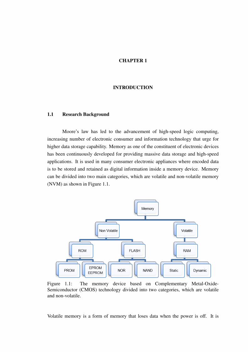
Moore’s law has led to the advancement of high-speed logic computing,increasing number of electronic consumer and information technology that urge forhigher data storage capability. Memory as one of the constituent of electronic deviceshas been continuously developed for providing massive data storage and high-speedapplications. It is used in many consumer electronic appliances where encoded datais to be stored and retained as digital information inside a memory device. Memorycan be divided into two main categories, which are volatile and non-volatile memory(NVM) as shown in Figure 1.1.
Figure 1.1: The memory device based on Complementary Metal-Oxide-Semiconductor (CMOS) technology divided into two categories, which are volatileand non-volatile.
Volatile memory is a form of memory that loses data when the power is off. It is

2
also referred as Random-Access-Memory (RAM) with very fast read and erase time.Dynamic-RAM (DRAM) and Static-RAM (SRAM) are the commonly known volatilememory. Whereas, non-volatile memory is a form of memory that preserves the dataeven when the power is off. It is also known as Read-Only-Memory (ROM). NVMcan retain massive amount of data but at lower write and read speed than the volatilememory. Mask ROM, Programmable ROM (PROM), Erasable PROM (EPROM),Electrically Erasable-Programmable ROM (EEPROM) and Flash Memory are thetypes of NVM. All of these memory devices are based on metal-oxide-semiconductor(MOS) technology. There are also other technologies that have been used to storedata. Optical devices such as compact-disk ROM (CD-ROM), digital-versatile-discRAM (DVD-RAM) and ferroelectric technology such as the well-known hard-diskdrive (HDD) are employed as dominant secondary memory, in which all of these arecommonly used to store digital information.
EEPROM provides with a practical usage of data storage device where theProgram/Erase (P/E) operation is performed by applying electric field to the transistorcell’s terminals. Furthermore, it also provides with byte-wise random access capabilitythat made EEPROM a key figure for data storage application and to perform execute-in-place (XiP) operation. However, each of EEPROM’s transistor cell or memory cellis form by two-transistor (2T), which made the device highly expensive and consumesvery large circuit layout for massive storage application [1]. Flash memory is anothertype of NVM that had been developed from EEPROM. Instead of having 2T per cell,flash memory only consists of one-transistor (1T) per cell and has been a revolution indirecting the course of memory industry into sub-20nm half-pitch scaling [2]. Becauseof its 1T per cell structure, the relative bit cost can be greatly reduced comparedto EEPROM and it has been vastly used in many today’s electronic appliances eversince. This has been proven based on a statistical study as shown in Figure 1.2(a) thatthe memory storage capacity exponentially increased within almost a decade (2007-2014). The emergence of mobile smart phone and solid state drive (SSD) have rapidlyincreased the storage capacity from 10,000 million GB to 70,000 million GB in a shortspan of four years (2010-2014). This has led to over 20% market share increment fromthe consolidation of some of the top semiconductor manufacturers such as Samsung,Micron, Hynix, Toshiba and SanDisk in which all of these companies hugely contributeto the manufacturing of mobile smart phone and SSD (refer Figure 1.2(b)).

3
(a)
(b)
Figure 1.2: (a) Number of storage capacity exponentially increase throughout the yearswith storage application devices is the highest. (Source from Forward Insight). (b)Memory revenue on some of the companies manufacturing various memory devicesand the top five companies consolidation in memory industry, majorly dominatedby companies that sold flash memory (source from Micron 2014 Winter AnalystConference).
1.2 Flash Memory Scaling Challenges and Motivation
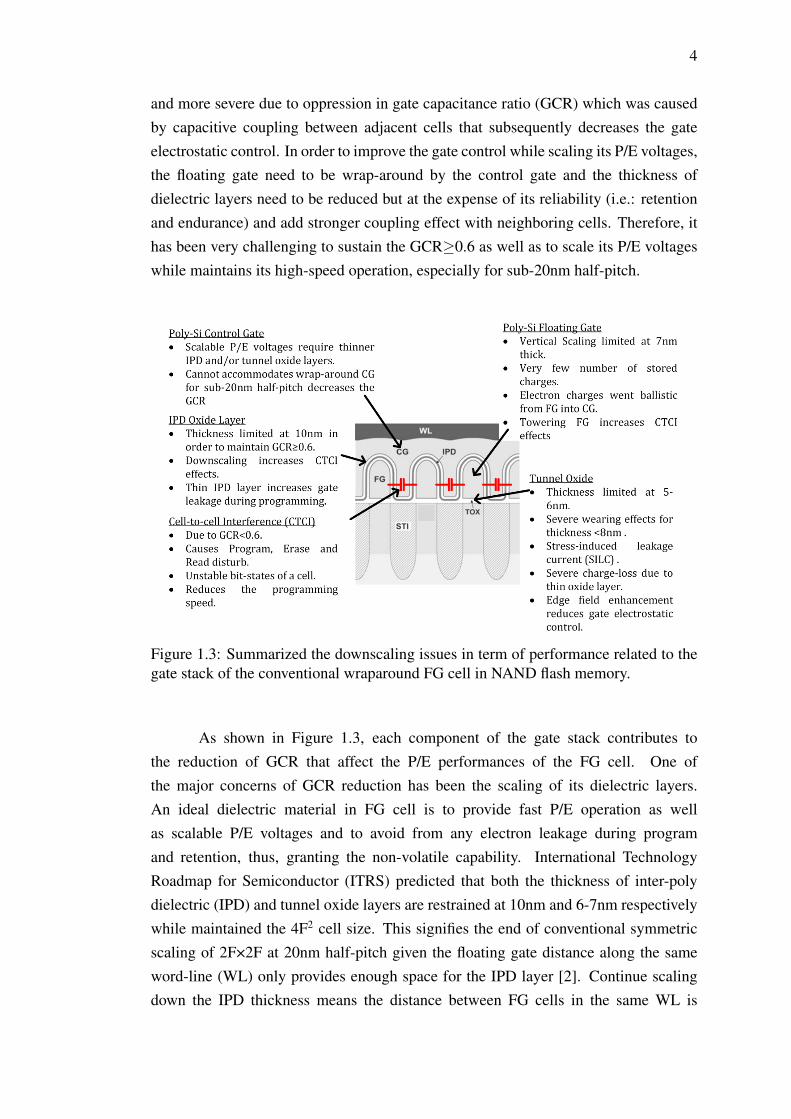
For more than two decades, floating gate (FG) memory cell has been commonlyutilized in many flash memory devices. To increase the storage capacity of flashmemory and to continue the exponential growth of the industry, scaling of FG cellis inevitable. However, downscaling of the FG cell has reached its bottleneck as thecell encounter physical limitations that degrade its memory performances. Figure 1.3summarizes the issues for each component of the gate stack of the FG cell (i.e.: poly-Si FG, poly-Si control gate, inter-poly dielectric and tunnel oxide) in understandingthe interrelation and the trade-off in their performances. These issues becoming more
4
and more severe due to oppression in gate capacitance ratio (GCR) which was causedby capacitive coupling between adjacent cells that subsequently decreases the gateelectrostatic control. In order to improve the gate control while scaling its P/E voltages,the floating gate need to be wrap-around by the control gate and the thickness ofdielectric layers need to be reduced but at the expense of its reliability (i.e.: retentionand endurance) and add stronger coupling effect with neighboring cells. Therefore, ithas been very challenging to sustain the GCR≥0.6 as well as to scale its P/E voltageswhile maintains its high-speed operation, especially for sub-20nm half-pitch.
Figure 1.3: Summarized the downscaling issues in term of performance related to thegate stack of the conventional wraparound FG cell in NAND flash memory.
As shown in Figure 1.3, each component of the gate stack contributes tothe reduction of GCR that affect the P/E performances of the FG cell. One ofthe major concerns of GCR reduction has been the scaling of its dielectric layers.An ideal dielectric material in FG cell is to provide fast P/E operation as wellas scalable P/E voltages and to avoid from any electron leakage during programand retention, thus, granting the non-volatile capability. International TechnologyRoadmap for Semiconductor (ITRS) predicted that both the thickness of inter-polydielectric (IPD) and tunnel oxide layers are restrained at 10nm and 6-7nm respectivelywhile maintained the 4F2 cell size. This signifies the end of conventional symmetricscaling of 2F×2F at 20nm half-pitch given the floating gate distance along the sameword-line (WL) only provides enough space for the IPD layer [2]. Continue scalingdown the IPD thickness means the distance between FG cells in the same WL is

5
getting cramped; as a result, the GCR will be reduced prior to stronger couplingwith neighboring floating gates. Moreover, to maintain the 4F2 cell size also impliesthat the distance between FG cells across the bit-line (BL) must be reduced creatingfringing capacitance not only across the BL but also with diagonal FG cells as well [3].This has added the variability to the threshold voltage of the selected cell and ledto abnormal cell-to-cell interference (CTCI) effects. Such effects are the unstablebit states of FG cell that caused disturb during P/E and read operations, and alsoreducing its speed [4, 5]. Therefore, with continuous downscaling the CTCI effectsare exponentially increased towards the 20nm half-pitch as shown in Figure 1.4(a).Other issue in scaling has been the floating gate itself as the electron charges continueto decrease with downscaling as shown in Figure 1.4(b). The figure also depicts theamount of critical electron charges before severe threshold voltage disturbance startto occur leading to unstable bit-state. In the case of tunnel oxide scaling, the high-field stress during P/E operation has caused severe wearing of the dielectric layerdue to the introduction of negative trapped charges [6]. With frequent P/E cycles thenegative trapped charges will steadily piled up and increases the threshold voltage,which subsequently degrades its dc (e.g.: Sub-threshold slope (SS), threshold voltagevariation) and transient performances (i.e.: retention) [7].
(a) (b)
Figure 1.4: Scaling limitation of 2-D NAND flash. (a) Increments in cell-to-cellinterference of a victim cell across BL, WL and diagonal FGs [4] and (b) decrementsin number of electron in floating gate.
Due to restraints and limitations in FG cell dielectric thickness, it is difficult toeffectively scale the 2-D NAND flash memory. Figure 1.5 shows the scaling projectionfrom some of the top flash memory manufacturers. In mid-2012, SanDisk defies thesymmetric 4F2 scaling of the FG cell and introduced the asymmetric 19nm×26nm percell to provide enough space for IPD layer and retain the wrap-around poly-Si controlgate technology. As flash memory continue to scale, it will only be a matter of time

6
before it reaches the horizon and stops at 10-12nm half-pitch due to the statistical limitsof charge stored inside the floating gate for beyond 10nm node. Therefore, an indefiniteincrease of memory storage may not be possible through device scaling. Instead, ithas been increased by stacking multiple layers of planar NAND array to form three-dimensional (3-D) NAND flash architecture [8]. However, stacking the conventionalplanar structure to form 3-D NAND flash requires additional photolithography processdepending on the number of layers, which is technically challenging and can be veryexpensive.
Figure 1.5: Roadmap from top semiconductor foundries for scaling 2-D and 3-DNAND flash architectures (source from ICinsight, 2014).
The emergence of Bit-Cost Scalable (BiCS) technology using ‘punch’ and‘plug’ process offers cheaper and higher number of vertical stack than conventionalplanar NAND flash memory [9]. Figure 1.6(a) depicts cheaper relative bit-cost forhigher number of stack compared to 3-D stacked planar NAND. The ‘punch’ and ‘plug’terms refer to the fabrication method that punch through multi-layer of electrodes andinsulators with single lithography process before plug holes with channel films to formGate-All-Around (GAA) transistor (refer Figure 1.6(b)). There are various types of3-D NAND flash being manufactured nowadays, in which all of these architecturesimplemented the GAA structure as their cell transistor and employed either floatinggate (FG) or charge-trapping (CT) as their memory element. Samsung and Toshibahave adopted the CT cell for their 3-D NAND namely the Terabit Cell Array Transistor(TCAT) and pipe-shaped Bit-Cost Scalable (p-BiCS) respectively [10, 11]. However,3-D CT NANDs are known to be susceptible to charge-spreading in the nitride-trapping layer that led to poor distribution of cell-state and degrades the retentioncharacteristics [12]. Therefore, some of the top semiconductor companies, such asHynix and Intel/Micron Flash Technologies (IMFT) preferred FG cell for their 3-D

7
NAND flash [13,14]. The reasons for maintaining floating gate as the memory elementin 3-D vertical NAND architectures are due to:
1. The 3-D stacked architecture with surrounding FG can circumvent the lateralcharge spreading that occurs in the charge trapping layer along the BL.
2. The poly-Si FG provides high energy barrier (3.15eV) from electron tunnelingduring retention.
(a) (b)
Figure 1.6: (a) Comparison of relative bit cost of 3-D architecture NAND flash betweenthe stacking of conventional 2-D planar NAND and Bit-Cost Scalable (BiCS) NANDtechnology as the number of layer increases. (b) BiCS fabrication method [9].
SK Hynix has been actively developing their 3-D FG NAND flash. Variousform of 3-D FG cells was proposed such as the Dual-Control Gate Surrounding-Floating Gate (DC-SF), the Separated-Sidewall Control Gate (S-SCG) and theSidewall Control Pillar (SCP). The most notable has been the SCP cell due toits capability of suppressing the interference effects, cell disturbances, fast P/Eoperation and accommodate downscaling to 20nm half-pitch. However, in early2016, it was IMFT that caught the attention of computer consumers by announcingtheir first generation 3-D vertical NAND [14]. The 3-D NAND cell is based onConventional-Floating Gate (C-FG) structure that uses the double poly-Si technologyand conventional P/E schemes. Due to its large physical cell size compared to the20nm NAND, better performance can be achieved. The wide memory window ofapproximately >10V is obtained indicating a greater number of electron stored inthe floating gate. This gives a good indication for Multi-Level Cell (MLC) and Tri-Level Cell (TLC) applications, where 256Gbit (MLC)/384Gbit (TLC) data per dieis expected to be stored in 32-layers vertical stack. The GAA structure also playsan important role in giving strong electrostatic gate control to improve the coupling

8
effects by aggressively reducing the total interference effects and threshold voltagedistribution in planar 20nm 2-D NAND by ~80% and ~50% respectively [14]. Largergate width/length ratio also added to its gate control capability to compensate the lowmobility of polysilicon channel and increases the string on-current. In addition, it isreported that the IMFT 3-D cell with 32-layer vertical stack has the highest bit densityof 1.52Gb/mm2 compared to Samsung CT cell of 1.01 Gb/mm2.
1.3 Problem Statements
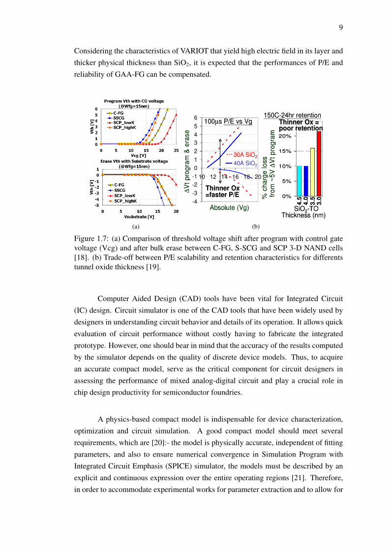
Although the 3-D FG cell possesses relevant number of reliability advantagesand high bit density compared to the 3-D CT cell, it also co-exists with cell-to-cellinterference causes by poor coupling at the floating gate and become more severe whenit comes to 3-D stacked architecture that led to higher programming voltage than its CTcounterpart [15]. As can be seen from Figure 1.7(a), C-FG cell requires higher programvoltage to yield wide threshold shift compared to SCP and S-SCG cells. Applyinghigh program voltage on a select cell can induce high-field at channel interface andspeedup the programming time, but this may eventually cause over-programming to itsneighboring cells. Thinning the tunnel oxide thickness can also boost the programmingspeed and provides scalable P/E voltages but increases the rate of electrons tunnelingback into the channel during retention. Figure1.7(b) depicts dramatic charge-loss inplanar CT cell for tunnel oxide thickness below 4nm. As for the case of FG cell, thetunnel oxide can hardly be scaled below 6-7nm to prevent from severe charge loss [2].Therefore, there has been a trade-off between scaling the tunnel oxide for scalableprogram voltage with data retention.
Nonetheless, given its conventional P/E schemes and less number of variabilityissues, the C-FG cell with GAA structure seems has been utilized as 3-D NAND flashmemory [14]. In order to provide fast program operation and 10 years data retention,the tunnel dielectric layer must be scaled. A tunnel barrier engineering concept knownas Variable Oxide Thickness (VARIOT) has been proposed through combinations oflow-k/high-k stack to deal with the trade-off of P/E characteristics performance withoutseverely jeopardizing the data retention capability [16, 17]. Govoreanu et. al., (2003)have shown that by stacking the high-k material such as ZrO2 on top of the low-kSiO2 can increase the gate tunneling current while very low current is observed at lowgate bias due to its thick physical thickness [16]. However, this method has yet to beutilized in 3-D FG cell leaving question marks to what combination of low-k/high-k that is suitable for boosting the P/E operation speed and retention characteristics.
9
Considering the characteristics of VARIOT that yield high electric field in its layer andthicker physical thickness than SiO2, it is expected that the performances of P/E andreliability of GAA-FG can be compensated.
(a) (b)
Figure 1.7: (a) Comparison of threshold voltage shift after program with control gatevoltage (Vcg) and after bulk erase between C-FG, S-SCG and SCP 3-D NAND cells[18]. (b) Trade-off between P/E scalability and retention characteristics for differentstunnel oxide thickness [19].
Computer Aided Design (CAD) tools have been vital for Integrated Circuit(IC) design. Circuit simulator is one of the CAD tools that have been widely used bydesigners in understanding circuit behavior and details of its operation. It allows quickevaluation of circuit performance without costly having to fabricate the integratedprototype. However, one should bear in mind that the accuracy of the results computedby the simulator depends on the quality of discrete device models. Thus, to acquirean accurate compact model, serve as the critical component for circuit designers inassessing the performance of mixed analog-digital circuit and play a crucial role inchip design productivity for semiconductor foundries.
A physics-based compact model is indispensable for device characterization,optimization and circuit simulation. A good compact model should meet severalrequirements, which are [20]:- the model is physically accurate, independent of fittingparameters, and also to ensure numerical convergence in Simulation Program withIntegrated Circuit Emphasis (SPICE) simulator, the models must be described by anexplicit and continuous expression over the entire operating regions [21]. Therefore,in order to accommodate experimental works for parameter extraction and to allow for
10
quick evaluation of circuitry or even discrete device performances, it is essential todevelop a compact model for GAA-FG.
To model the electrical behaviour of GAA-FG cell, the GAA nanowire-FET (GAANWFET) core models must be comprehended. There are two typesof GAANWFET which are the conventional GAANWFET and the most recent,junctionless-based GAANWFET or known as Junctionless Nanowire Transistor (JNT).Although there have been numerous works on compact modeling of GAANWFETs,especially for the conventional one, there are opportunities for further refinement. Itcan be described as follows;
For conventional GAANWFET:-
1. Several attempts are made to explicitly solve the arbitrary body-dopedGAANWFET [22–24]. But the models are limited for dopant concentrationup to 5×1018 cm-3 despite having empirical parameters being used [23] andneglected the importance of trap states along the channel for a realistic compactmodel. Furthermore, some of the models have also assumed zero flat-bandvoltage to fit the numerical TCAD simulation, which is physically unreasonable[24, 25].
2. Another important feature in GAANWFET is the partial-depletion conductionin highly-doped condition. Most of the models developed for GAANWFETinvoked the full-depletion approximation to simplify the nonlinearity ofPoisson’s equation so that it can be integrated across the channel length. Thus,the model is accurate only for fully-depleted device and limited to doping-geometry ratio up to 0.45 [23, 26–31] that can lead to misinterpretation ofits subthreshold performance. An attempt to include the partial-depletionconduction and to extend the validity of doping-geometry ratio only results inpoor accuracy to its low-doped body condition [32].
For Junctionless Nanowire Transistor (JNT):-
1. Most models reported for JNT are regional, and the current expressions arepiecewise continuous, where additional smoothing functions that rely on fittingparameters are required to unify between regions [33–38]. In addition, thereare other JNT models that are continuous but took an implicit form [39–41].The implicit form solution requires iterative numerical method, which either

11
converges very slowly or does not converge due to imaginary value [42].Therefore, a nonpiecewise continuous and explicit model is required for JNT.
2. Quasi-static terminal charges and capacitance are essential for ac and transientsimulation. As far as this work is concerned, there are very few works thatprovide with analytical solution of terminal charges and capacitnace for JNT [20,43]. The developed solution for these parameters involves additional smoothingfunctions and rely on fitting parameters to fit the graph despite suffering in termsof accuracy as much as 16% [43]. While other, requires demanding derivationprocesses using partial derivative in solving the capacitance [20].
1.4 Research Objectives
The mutual target of this research is to design and enhance the performanceof GAA-FG cell by implementing the concept of VARIOT and to develop its compactmodel using charge-based explicit expression. Based on the limitations and trade-offs in C-FG cell, also considering the performance expectation of VARIOT as thetunnel oxide layer, and the modeling issues in GAANWFET devices, the objectivesare summarized as follow:
1. To optimize and determine a suitable VARIOT combination of low-k/high-kstack for GAA-FG cell in compensating the trade-off between P/E and retentioncharacteristics.
2. Compact model of conventional GAANWFET:-
(a) To explicitly solve the mobile charge density for arbitrary body dopingincluding the trap state effects.
(b) To analytically model the partial-depletion conduction.
3. Compact model of Junctionless Nanowire Transistor:-
(a) To explicitly solve the mobile charge density that is continuous for alloperating regions.
(b) To obtain a continuous drain current, terminal charges and capacitanceexpressions.
4. To model the floating gate potential of GAA-FG.

12
1.5 Research Scopes
The scopes of this research will be confined as follows:
1. GAA-FG Design: The dimension and physical parameters of GAA-FG arebased on experimental work performed by Lee et al., (2013) [44]. Althoughthe experimental data by Lee et al., (2013) has used triangular nanowire asthe channel, but in order to comply with vertical channel fabrication processthe cylindrical channel has been used in this simulation work. In addition,the physical transport between triangular and cylindrical channels remain thesame. Barrier Engineered of VARIOT tunnel oxide is limited to asymmetriccombinations of low-k/high-k stack given the relevance for enhancing programoperation and retention performances.
2. Simulation Work: Technological-Computer-Aided-Design (TCAD) simulationwork is divided into two parts; parameters optimization and device simulation ofGAA-FG. Based on MOS capacitor (MOS-C) structure and for a given flashmemory constraint, extensive parameter optimization is conducted to obtainoptimum parameter settings. Device simulation is performed to observe andanalyze the transfer characteristics and transient memory performances of adiscrete single-cell/transistor GAA-FG. Under this condition, the effects fromneighbouring cell are omitted.
3. Analytical Modeling: Device compact modeling of GAA-FG, which involvesobtaining the explicit expression of mobile charge densities for GAA nanowire-FET, and the floating gate potential model. The compact model is limited to theessence of core model, which are long-channel and constant mobility. Therefore,the compact model does not include advanced physical effects. The accuracyof the explicit expression is discussed based on the accuracy of previouslypublished works and 3-D device simulation over practical terminal voltages.
1.6 Research Contribution
The significant contribution of this work can be highlighted as follow:-
1. Optimization of VARIOT: The optimization of VARIOT tunnel layer that consistsof low-k/high-k stack is performed for various high-k materials in order todetermine their optimum thickness and to extract its tunneling properties. The
13
extracted optimum thickness for various low-k/high-k stack can be used as atunnel oxide layer in a memory cell devices. Given the nonlinear behaviour oftunnel barrier engineering, the tunneling properties of VARIOT such as Fowler-Nordheim (F-N) coefficients can be exploited by circuit designer in analyzingthe P/E performances of a memory cell or even to analyze the effect of gateleakage in a MOSFET device that uses VARIOT as its gate oxide.
2. GAA-FG with VARIOT tunnel layer: Subsequent to the optimization of VARIOT,the optimized thickness of low-k/high-k stacks are employed as a tunnel layer inGAA-FG cell to improve its P/E characteristics as well as its data retention.
3. Explicit and continuous compact model of GAA devices: To the relevance ofGAA-FG cell that adopted nanowire structure, the compact model of nanowiredevices, which are the GAANWFET and the JNT are developed. In thisstudy, due to the importance of highly-doped body of GAANWFET, the partial-depletion conduction is considered in improving the accuracy of the compactmodel. For the sake of avoiding numerical convergence and piecewise model,an explicit nonpiecewise and continuous compact model of JNT is developed.
1.7 Thesis Organization
Chapter 1 is the foundation of this research. A brief background on memorydevices and its development throughout the years in highlighting on memory storagedemand due to rapid technology advancement that prompt to the importance of flashmemory. Then, scaling challenges and motivations of flash memory are highlightedthat deduced the problem statements. Based on the problem statements, researchobjectives are identified. The scope of work has been clarified depending on theexisting experimental and tools provided. Finally, the contributions of this work arehighlighted.
Chapter 2 covers broad overview on 3-D NAND cell structures, whereadvantages and disadvantages from each structure are being highlighted. Inconjunction with VARIOT tunnel layer, the concept of barrier engineering is discussedbased on the types of dielectric stacking as well as its physical transport. Devicemodeling is briefly described before in-depth review on modeling approach of GAAnanowire-FET and floating gate potential modeling are discussed.
Chapter 3 discusses the research method of this work starting from general flow
14
and technical works that are being conducted in achieving the objectives. The tools thatwere used in this research are also highlighted. Furthermore, details on the approachtaken in simulation work such as dielectric material, optimization method and physicalmodels, and also compact modeling work such as model-flow and approximationtechniques are presented in the form flowchart and discussed.
In Chapter 4, all the simulation results are presented, which includesoptimization of VARIOT and characterization of GAA-FG in determining whichVARIOT combination is the most prowess for its application as memory cell inproviding fast P/E operation as well as 10 years data retention. As a consequent tosimulation work of GAA-FG, Chapter 5 provides with a comprehensive explanation onanalytical modeling with regards to all the issues highlighted in the research problem,until the compact model for GAA-FG is concluded.
Finally, Chapter 6 summarizes all the findings in this research and thecontributions are highlighted. In addition, to ensure the continuation of this researchand to add more promising contributions to compact model society, future works areprovided.

REFERENCES
1. Bez, R., Camerlenghi, E., Modelli, A. and Visconti, A. Introduction to flashmemory. Proceedings of the IEEE. 2003, vol. 91. 489–502.
2. International Technology Roadmap for Semiconductors (ITRS). Process
Integration, Devices and Structure. Technical report. 2013.
3. Kim, Y. J., Kang, J. G., Lee, B., Cho, G.-S., Park, S.-K. and Choi, W. Y.Effects of abnormal cell-to-cell interference on p-type floating gate andcontrol gate NAND flash memory. Japanese Journal of Applied Physics,2014. 53(4S): 04ED12.
4. Prall, K. Scaling Non-Volatile Memory Below 30nm. Non-Volatile
Semiconductor Memory Workshop, 2007 22nd IEEE. 2007. 5–10.
5. Van Houdt, J. Flash memory: a challenged memory technology. 2006
IEEE International Conference on Integrated Circuit Design and Technology,
Proceedings. 2006. 40–43.
6. Keeney, S. N. Dielectric Scaling Challenges and Approches In Floating GateNon-Volatile Memories. Proceedings of Electrochemical Society. 2004. 151–158.
7. Ielmini, D. Overview of Modeling Approaches for Scaled Non VolatileMemories. 2009 International Conference on Simulation of Semiconductor
Processes and Devices. IEEE. 2009. 1–8.
8. Jung, S. M., Jang, J., Cho, W., Cho, H., Jeong, J., Chang, Y., Kim, J., Rah,Y., Son, Y., Park, J., Song, M. S., Kim, K. H., Lim, J. S. and Kim, K.Three dimensionally stacked NAND flash memory technology using stackingsingle crystal Si layers on ILD and TANOS structure for beyond 30nm node.Technical Digest - International Electron Devices Meeting, IEDM. 2006.30–33.
9. Tanaka, H., Kido, M., Yahashi, K., Oomura, M., Katsumata, R., Kito, M.,Fukuzumi, Y., Sato, M., Nagata, Y., Matsuoka, Y., Iwata, Y., Aochi, H. andNitayama, A. Bit Cost Scalable Technology with Punch and Plug Process forUltra High Density Flash Memory. VLSI Technology, 2007 IEEE Symposium

158
on. 2007. 14–15.
10. Jang, J., Kim, H.-S., Cho, W., Cho, H., Kim, J., Shim, S. I., Jang, Y., Jeong,J.-H., Son, B.-K., Kim, D. W., Kim, K., Shim, J.-J., Lim, J. S., Kim, K.-H., Yi, S. Y., Lim, J.-Y., Chung, D., Moon, H.-C., Hwang, S., Lee, J.-W.,Son, Y.-H., Chung, U.-I. and Lee, W.-S. Vertical Cell Array Using TCAT(Terabit Cell Array Transistor) Technology for Ultra High Density NANDFlash Memory. 2009 Symposium on VLSI Technology. 2009. 14–15.
11. Nitayama, A. and Aochi, H. Bit Cost Scalable (BiCS) flash technologyfor future ultra high density storage devices. VLSI Technology Systems and
Applications (VLSI-TSA), 2010 International Symposium on. 2010. 130–131.
12. Kang, C., Choi, J., Sim, J., Lee, C., Shin, Y., Park, J., Sel, J., Jeon, S., Park,Y. and Kim, K. Effects of Lateral Charge Spreading on the Reliability ofTANOS (TaN/AlO/SiN/Oxide/Si) NAND Flash Memory. Reliability physics
symposium, 2007. proceedings. 45th annual. ieee international. 2007. 167–170.
13. Aritome, S., Whang, S., Lee, K., Shin, D., Kim, B., Kim, M., Bin, J., Han,J., Kim, S., Lee, B., Jung, Y., Cho, S., Shin, C., Yoo, H., Choi, S., Hong,K., Park, S. and Hong, S. A novel three-dimensional dual control-gate withsurrounding floating-gate (DC-SF) NAND flash cell. Solid-State Electronics,2013. 79(January): 166–171.
14. Parat, K. and Dennison, C. A floating gate based 3D NAND technologywith CMOS under array. Technical Digest - International Electron Devices
Meeting, IEDM. 2016. 3.3.1–3.3.4.
15. Micheloni, R. 3D Flash Memories. 1st ed. Springer. 2016.
16. Govoreanu, B., Blomme, P., Van Houdt, J. and De Meyer, K. Enhancedtunneling current effect for nonvolatile memory applications. Japanese
Journal of Applied Physics, Part 1: Regular Papers and Short Notes and
Review Papers, 2003. 42(4B): 2020–2024.
17. Govoreanu, B., Blomme, P., Rosmeulen, M., Van Houdt, J. and De Meyer,K. VARIOT: a novel multilayer tunnel barrier concept for low-voltagenonvolatile memory devices. Electron Device Letters, IEEE, 2003. 24(2):99–101.
18. Seo, M. S., Choi, J. M., Park, S. K. and Endoh, T. Highly scalable 3-Dvertical FG NAND cell arrays using the Sidewall Control Pillar (SCP). 2012
4th IEEE International Memory Workshop, IMW 2012. 2012. 1–4.
19. Gilmer, D. C., Goel, N., Park, H., Park, C., Verma, S., Bersuker, G.,

159
Lysaght, P., Tseng, H.-H., Kirsch, P. D., Saraswat, K. C. and Jammy,R. Engineering the complete MANOS-type NVM stack for best in classretention performance. 2009 IEEE International Electron Devices Meeting
(IEDM). IEEE. 2009. 1–4.
20. Jiang, C., Liang, R., Xu, J. and Alam, M. A. A Compact Quasi-StaticTerminal Charge and Drain Current Model for Double-Gate JunctionlessTransistors and Its Circuit Validation. IEEE Transactions on Electron
Devices, 2017. 64(12): 4823–4830.
21. Yu, B., Lu, H., Liu, M. and Taur, Y. Explicit Continuous Models for Double-Gate and Surrounding-Gate MOSFETs. IEEE Transactions on Electron
Devices, 2007. 54(10): 2715–2722.
22. He, J., Bian, W., Zhang, J., Feng, J., Zhang, X., Wu, W. and Chan,M. An explicit carrier-based compact model for nanowire surrounding-gateMOSFET simulation. Molecular Simulation, 2008. 34(1): 81–87.
23. Cheralathan, M., Cerdeira, A. and Benjamin, I. Compact model for long-channel cylindrical surrounding-gate MOSFETs valid from low to highdoping concentrations. Solid-State Electronics, 2011. 55(1): 13–18.
24. Jin, X., Liu, X., Wu, M., Chuai, R., Lee, J.-H. and Lee, J.-H. A ContinuousCurrent Model of Ultra-Thin Cylindrical Surrounding-Gate Inversion-ModeSi Nanowire nMOSFETs Considering a Wide Range of Body DopingConcentration. Semiconductor Science and Technology, 2013. 28(1): 15002.
25. Jin, X.-S., Liu, X., Hyuck-In, K. and Jong-Ho, L. A Continuous CurrentModel of Accumulation Mode (Junctionless) Cylindrical Surrounding-GateNanowire MOSFETs. Chin. Phys. Lett., 2013. 30(3): 038502.
26. Liu, F., He, J., Zhang, L., Zhang, J., Hu, J., Ma, C. and Chan, M. A charge-based model for long-channel cylindrical surrounding-gate MOSFETs fromintrinsic channel to heavily doped body. IEEE Transactions on Electron
Devices, 2008. 55(8): 2187–2194.
27. Liu, F., He, J., Zhang, L., Zhang, J., Hu, J., Zhang, X. and Chan, M. Acomplete charge based compact model for silicon nanowire FETs includingdoping and advanced physical effects. 2008. 157–160.
28. Yu, Y. S., Cho, N., Hwang, S. W. and Ahn, D. Implicit ContinuousCurrent-Voltage Model for Surrounding-Gate Metal-Oxide-SemiconductorField-Effect Transistors Including Interface Traps. IEEE Transactions on
Electron Devices, 2011. 58(8): 2520–2524.
29. Liu, F., Zhang, J., He, F., Liu, F., Zhang, L. and Chan, M. A charge-based

160
compact model for predicting the current-voltage and capacitance-voltagecharacteristics of heavily doped cylindrical surrounding-gate MOSFETs.Solid-State Electronics, 2009. 53(1): 49–53.
30. Cheng, Q., Hong, C., Kuo, J. B. and Chen, Y. A surface-field-based modelfor nanowire MOSFETs with spatial variations of doping profiles. IEEE
Transactions on Electron Devices, 2014. 61(12): 4040–4046.
31. Hong, C., Cheng, Q., Wang, P., Meng, W., Yang, L., Kuo, J. B. andChen, Y. An Analytic Surface-Field-Based Quasi-Atomistic Model forNanowire MOSFETs with Random Dopant Fluctuations. IEEE Transactions
on Electron Devices, 2015. 62(12): 4179–4185.
32. Zhang, L., Zhang, J., Liu, F., Chen, L., Xu, Y., Zhou, W. and He, F. Ananalytic channel potential based model for dynamic depletion surrounding-gate mosfets with arbitrary doping level. 2009 1st Asia Symposium on Quality
Electronic Design. 2009. 131–135.
33. Gnani, E., Gnudi, A., Reggiani, S. and Baccarani, G. Theory of theJunctionless Nanowire FET. IEEE Transactions on Electron Devices, 2011.58(9): 2903–2910.
34. Sallese, J. M., Chevillon, N., Lallement, C., Iñiguez, B. and Prégaldiny, F.Charge-based modeling of junctionless double-gate field-effect transistors.IEEE Transactions on Electron Devices, 2011. 58(8): 2628–2637.
35. Chen, Z., Xiao, Y., Tang, M., Xiong, Y., Huang, J., Li, J., Gu, X. and Zhou,Y. Surface-potential-based drain current model for long-channel junctionlessdouble-gate MOSFETs. IEEE Transactions on Electron Devices, 2012.59(12): 3292–3298.
36. Lime, F., Santana, E. and Iñiguez, B. A simple compact model for long-channel junctionless Double Gate MOSFETs. Solid-State Electronics, 2013.80: 28–32.
37. Lime, F., Moldovan, O. and Iniguez, B. A compact explicit model for long-channel gate-all-around junctionless MOSFETs. Part I: DC characteristics.IEEE Transactions on Electron Devices, 2014. 61(9): 3036–3041.
38. Hwang, B. W., Yang, J. W. and Lee, S. H. Explicit analytical current-voltage model for double-gate junctionless transistors. IEEE Transactions
on Electron Devices, 2015. 62(1): 171–177.
39. Duarte, J. P., Choi, S. J., Moon, D. I. and Choi, Y. K. A nonpiecewise modelfor long-channel junctionless cylindrical nanowire FETs. IEEE Electron
Device Letters, 2012. 33(2): 155–157.
161
40. Hong, C., Yang, L., Cheng, Q., Han, T., Kuo, J. and Chen, Y. A ContinuousCompact Model Incorporating Higher-Order Correction for JunctionlessNanowire Transistors with Arbitrary Doping Profiles. IEEE Transactions
on Nanotechnology, 2016. PP(99): 1–8.
41. Hong, C., Yang, L., Cheng, Q., Han, T., Kuo, J. B. and Chen, Y. A NonlinearSurface-Field Compact Model for Junctionless Nanowire MOSFETs. 2016
IEEE Workshop on Microelectronics and Electron Devices (WMED). 2016.8–11.
42. Jandhyala, S. and Mahapatra, S. An Efficient Robust Algorithm forthe Surface-Potential Calculation of Independent DG MOSFET. IEEE
Transactions on Electron Devices, 2011. 58(6): 1663–1671.
43. Moldovan, O., Lime, F. and Iniguez, B. A Compact Explicit Model for Long-Channel Gate-All-Around Junctionless MOSFETs. Part II: Total Chargesand Intrinsic Capacitance Characteristics. IEEE Transactions on Electron
Devices, 2014. 61(9): 3042–3046.
44. Lee, K.-H., Lin, H.-c. and Huang, T.-y. Gate-All-Around Floating-GateMemory Device with Triangular Poly-Si Nanowire Channels. Japanese
Journal of Applied Physics, 2013. 14: 532–533.
45. Lee, K.-H., Tsai, J.-R., Chang, R.-D., Lin, H.-C. and Huang, T.-Y. Low-Voltage High-Speed Programming/Erasing Floating-Gate Memory Devicewith Gate-All-Around Polycrystalline Silicon Nanowire. Applied Physics
Letters, 2013. 103: 153102.
46. Endoh, T., Kinoshita, K., Tanigami, T., Wada, Y., Sato, K., Yamada, K.,Yokoyama, T., Takeuchi, N., Tanaka, K., Awaya, N., Sakiyama, K. andMasuoka, F. Novel Ultra High Density Flash Memory with A Stacked-Surrounding Gate Transistor (S-SGT) Structured Cell. International Electron
Devices Meeting, 2001. IEDM ’01. Technical Digest. 2001. 2.3.1–2.3.4.
47. Seo, M. S., Park, S. K. and Endoh, T. The 3-Dimensional Vertical FG NANDFlash Memory with a Novel Electrical S/D Technique Using the ExtendedSidewall Control Gate (ECSG). IEEE Transactions on Electron Devices.2011, vol. 58. 2966–2973.
48. Seo, M. S., Lee, B. H., Park, S. K. and Endoh, T. A Novel 3-DVertical FG NAND Flash Memory Cell Arrays Using the Separated SidewallControl Gate (S-SCG) for Highly Reliable MLC Operation. 2011 3rd IEEE
International Memory Workshop, IMW 2011. 2011. 1–4.
49. Whang, S., Lee, K., Shin, D., Kim, B., Kim, M., Bin, J., Han, J., Kim, S.,

162
Lee, B., Jung, Y., Cho, S., Shin, C., Yoo, H., Choi, S., Hong, K., Aritome, S.,Park, S. and Hong, S. A Novel Three-Dimensional Dual Control-Gate withSurrounding Floating-Gate (DC-SF) NAND Flash Cell for 1Tb File StorageApplication. Solid-State Electronics. 2010, vol. 79. 166–171.
50. Aritome, S., Noh, Y., Yoo, H., Choi, E. S., Joo, H. S., Ahn, Y., Han, B.,Chung, S., Shim, K., Lee, K., Kwak, S., Shin, S., Choi, I., Nam, S., Cho, G.,Sheen, D., Pyi, S., Choi, J., Park, S., Kim, J., Lee, S., Hong, S., Park, S. andKikkawa, T. Advanced DC-SF Cell Technology for 3-D NAND Flash. IEEE
Transactions on Electron Devices, 2013. 60(4): 1327–1333.
51. Seo, M. S., Lee, B. H., Park, S. K. and Endoh, T. Novel Concept of theThree-Dimensional Vertical FG Nand Flash Memory using the Separated-Sidewall Control Gate. IEEE Transactions on Electron Devices, 2012. 59(8):2078–2084.
52. Likharev, K. K. Layered tunnel barriers for nonvolatile memory devices.Applied Physics Letters, 1998. 73(15): 2137–2139.
53. Allyn, C. L., Gossard, A. C. and Wiegmann, W. New rectifyingsemiconductor structure by molecular beam epitaxy. Applied Physics Letters,1980. 36(5): 373–376.
54. Gehring, A. and Selberherr, S. Modeling of tunneling current and gatedielectric reliability for nonvolatile memory devices. IEEE Transactions on
Device and Materials Reliability, 2004. 4(3): 306–319.
55. Jain, S., Neema, V., Gupta, D. and Vishvakarma, S. K. Investigation ofBand-Gap Engineered Silicon-Oxide-Nitride-Oxide-Silicon Flash Memorywith High-k Dielectrics in Tunnel Barrier and Its Impact on Charge RetentionDynamics. Journal of Nanoelectronics and Optoelectronics, 2016. 11: 6–11.
56. Jain, S., Gupta, D., Neema, V. and Vishwakarma, S. BE-SONOS flashmemory along with metal gate and high- k dielectrics in tunnel barrier andits impact on charge retention dynamics. Journal of Semiconductors, 2016.37(3): 1–6.
57. You, H. W., Son, J. W. and Cho, W. J. Engineering of tunnel barrier for highlyintegrated nonvolatile memory applications. Applied Physics A: Materials
Science and Processing, 2011. 102(4): 921–926.
58. Padovani, A., Larcher, L., Verma, S., Pavan, P., Majhi, P., Kapur, P.,Parat, K., Bersuker, G. and Saraswat, K. Statistical Modeling of LeakageCurrents Through SiO2/High-κ Dielectrics Stacks for Non-Volatile MemoryApplications. 2008 IEEE International Reliability Physics Symposium. IEEE.
163
2008. 616–620.
59. Verma, S. Tunnel Barrier Engineering For Flash Memory Technology. Ph.D.Thesis. 2010.
60. Blomme, P., Govoreanu, B., Rosmeulen, M., Akeyar, A., Haspeslagh, L., DeVos, J., Lorenzini, M., Van Houdt, J. and De Meyer, K. High-κ MaterialsFor Tunnel Barrier Engineering in Future Memory Technologies. ECS
Transactions. 2006, vol. 1. 75–89.
61. Driussi, F., Marcuzzi, S., Palestri, P. and Selmi, L. Gate current in stackeddielectrics for advanced FLASH EEPROM cells. Proceedings of ESSDERC
2005: 35th European Solid-State Device Research Conference. 2005, vol.2005. 317–320.
62. Srikantaiah, J. G. and DasGupta, A. Quantum mechanical effects in bulkMOSFETs from a compact modeling perspective: A review. IETE Technical
Review (Institution of Electronics and Telecommunication Engineers, India),2012. 29(1): 3–28.
63. Iniguez, B. and Moreno, E. G. Development of a C-continuous small-signalmodel for a MOS transistor in normal operation. IEEE Transactions on
Computer-Aided Design of Integrated Circuits and Systems, 1995. 14(2):163–166.
64. Iniguez, B., Ferreira, L., Gentinne, B. and Flandre, D. A Physically-Based C-Continuous Fully-Depleted SOI MOSFET Model for Analog Applications.IEEE Trans. Electron Devices, 1996. 43(4): 568–575.
65. Iniguez, B. and Moreno, E. G. An Improved C ∞-Continuous Small-Geometry MOSFET Modeling for Analog Applications. Analog Integrated
Circuits and Signal Processing, 1997. 259(13): 241–259.
66. Miura-Mattausch, M., Feldmann, U., Rahm, A. and Bollu, M. UnifiedComplete Mosfet Model For Analysis Of Digital And Analog Circuits.Computer-Aided Design, 1994., IEEE/ACM International Conference on,1994. 15(1): 264–267.
67. Gildenblat, G., Member, S., Wang, H., Member, S., Chen, T.-l. and Gu, X.SP : An Advanced Surface-Potential-Based Compact MOSFET Model. IEEE
Journal of Solid-State Circuits, 2004. 39(9): 1394–1406.
68. Byun, Y. H., Lee, K. and Shur, M. Unified Charge Control Model andSubthreshold Current in Heterostructure Field-Effect Transistors. IEEE
Electron Device Letters, 1990. 11(1): 50–53.

164
69. Maher, M. A. and Mead, C. A. A physical charge-controlled model for MOStransistors. Advanced Research in VLSI. Proceedings of the 1987 Stanford
Conference. 1987. 211–229.
70. Cunha, A., Schneider, M. C. and Galup-Montoro, C. An Explicit PhysicalModel for the Long-Channel Transistor Small-Signal Parameters. Solid State
Electronics, 1995. 38(11): 1945–1952.
71. Tsividis, Y. Operation and Modeling of the Mos Transistor (The Oxford
Series in Electrical and Computer Engineering). Oxford University Press.2004.
72. Cunha, A. I. A., Schneider, M. C. and Galup-Montoro, C. Derivation of theunified charge control model and parameter extraction procedure. Solid-State
Electronics, 1999. 43(3): 481 – 485.
73. Iniguez, B., Jiminez, D., Roig, J., Hamid, H. A., Marsal, L. F. and Pallares,J. Explicit continuous model for long-channel undoped surrounding gateMOSFETs. IEEE Transactions on Electron Devices, 2005. 52(8): 1868–1873.
74. Kundert, K. The Design’s Guide to SPICE and Spectre, Springer, chap. 2(DC Analysis). 1995, 15–22.
75. Rios, R., Mudanai, S., Shih, W.-K. and Packan, P. An efficient surfacepotential solution algorithm for compact MOSFET models. IEDM Technical
Digest. IEEE International Electron Devices Meeting, 2004. 2004. 755–758.
76. Turchetti, C. and Masetti, G. A CAD-Oriented Analytical MOSFET Modelfor High-Accuracy Applications. IEEE Transactions on Computer-Aided
Design of Integrated Circuits and Systems, 1984. 3(2): 117–122.
77. Chen, T. L. and Gildenblat, G. Analytical approximation for the MOSFETsurface potential. Solid-State Electronics, 2005. 49(2): 267–270.
78. Sacchetto, D., Ben-Jamaa, M. H., DeMicheli, G. and usuf Leblebici, Y.Fabrication and characterization of vertically stacked Gate-All-Around SiNanowire FET arrays. 2009 Proceedings of the European Solid State Device
Research Conference. IEEE. 2009. 245–248.
79. Buddharaju, K. D., Singh, N., Rustagi, S. C., Teo, S. H. G., Wong, L. Y.,Tang, L. J., Tung, C. H., Lo, G. Q., Balasubramanian, N. and Kwong, D. L.Gate-all-around Si-nanowire CMOS inverter logic fabricated using top-downapproach. European Solid-State Device Research Conference. 2007. 303–306.

165
80. Oh, S.-H., Monroe, D. and Hergenrother, J. Analytic description of short-channel effects in fully-depleted double-gate and cylindrical, surrounding-gate MOSFETs. IEEE Electron Device Letters, 2000. 21(9): 3–6.
81. Auth, C. P. and Plummer, J. D. Scaling theory for cylindrical, fully-depleted,surrounding-gate MOSFET’s. IEEE Electron Device Letters, 1997. 18(2):74–76.
82. Paydavosi, N., Venugopalan, S., Chauhan, Y. S., Duarte, J. P., Jandhyala, S.,Niknejad, A. M. and Hu, C. C. BSIM-SPICE Models Enable FinFET andUTB IC Designs. IEEE Access, 2013. 1: 201–215.
83. Jiménez, D., Iníguez, B., Suné, J., Marsal, L. F., Pallarès, J., Roig, J. andFlores, D. Continuous analytic I-V model for surrounding-gate MOSFETs.IEEE Electron Device Letters, 2004. 25(8): 571–573.
84. Chen, Y. and Luo, J. A comparative study of double-gate and surrounding-gate MOSFETs in strong inversion and accumulation using an analyticalmodel. Technical Proceedings of the 2001 International Conference on
Modeling and Simulation of Microsystems. 2001, vol. 1. 546–549.
85. Yu, B., Lu, W.-Y., Lu, H. and Taur, Y. Analytic Charge Model forSurrounding-Gate MOSFETs. IEEE Transactions on Electron Devices, 2007.54(3): 492–496.
86. Jiménez, D., Sáenz, J. J., Iñíguez, B., Member, S., Suñé, J., Member, S.,Marsal, L. F. and Pallarès, J. Modeling of Nanoscale Gate-All-AroundMOSFETs. IEEE Electron Device Letters, 2004. 25(5): 314–316.
87. Sadhu, J. S., Tian, H., Spila, T., Kim, J., Azeredo, B., Ferreira, P. and Sinha,S. Controllable doping and wrap-around contacts to electrolessly etchedsilicon nanowire arrays. Nanotechnology, 2014. 25(37): 375701.
88. Balestra, F., Benachir, M., Brini, J. and Ghibaudo, G. Analytical Models ofSubthreshold Swing and Threshold Voltage for Thin- and Ultra-Thin-FilmSOI MOSFETs. IEEE Transactions on Electron Devices, 1990. 37(11):2303–2311.
89. Lee, M., Moon, T. and Kim, S. Floating Body Effect in Partially DepletedSilicon Nanowire Transistors and Potential Capacitor-Less One-TransistorDRAM Applications. IEEE Transactions on Nanotechnology, 2012. 11(2):355–359.
90. Sherony, M. J., Wei, A. and Antoniadis, D. A. Effect of body-charge on fully-and partially-depleted SOI MOSFET design. International Electron Devices
Meeting. Technical Digest. 1996. 125–128.
166
91. Wei, L., Chen, Z., Roy, K., Johnson, M. C., Ye, Y. and De, V. K.Design and optimization of dual-threshold circuits for low-voltage low-powerapplications. IEEE Transactions on Very Large Scale Integration (VLSI)
Systems, 1999. 7(1): 16–24.
92. He, J., Liu, F., Bian, W., Feng, J., Zhang, J. and Zhang, X. An approximatecarrier-based compact model for fully depleted surrounding-gate MOSFETswith a finite doping body. Semiconductor Science and Technology, 2007.22(6): 671–677.
93. Duarte, J. P., Choi, S. J., Moon, D. I., Ahn, J. H., Kim, J. Y., Kim, S. and Choi,Y. K. A Universal Core Model for Multiple-Gate Field-Effect Transistors.Part I: Charge Model. IEEE Transactions on Electron Devices, 2013. 60(2):840–847.
94. Duarte, J. P., Choi, S. J., Moon, D. I., Ahn, J. H., Kim, J. Y., Kim, S. and Choi,Y. K. A Universal Core Model for Multiple-Gate Field-Effect Transistors.Part II: Drain Current Model. IEEE Transactions on Electron Devices, 2013.60(2): 848–855.
95. Cheralathan, M., Iannaccone, G., Sangiorgi, E. and Iiguez, B. Analyticaldrain current model reproducing advanced transport models in nanoscalecylindrical surrounding-gate (SRG) MOSFETs. Journal of Applied Physics,2011. 110(3): 1–5.
96. Amakawa, S., Nakazato, K. and Mizuta, H. A surface-potential-basedcylindrical surrounding-gate MOSFET model. (2): 3–4.
97. He, J., Bian, W., Tao, Y., Yang, S. and Tang, X. Analytic carrier-basedcharge and capacitance model for long-channel undoped surrounding-gateMOSFETs. IEEE Transactions on Electron Devices, 2007. 54(6): 1478–1485.
98. Zhou, X., Zhu, G., See, G. H., Chandrasekaran, K., Chiah, S. B. and Lim,K. Y. Unification of MOS Compact Models with the Unified RegionalModeling Approach. J. Comput. Electron., 2011. 10(1-2): 121–135.
99. Dunga, M. V., Lin, C. H., Xi, X., Lu, D. D., Niknejad, A. M. and Hu,C. Modeling Advanced FET Technology in a Compact Model. IEEE
Transactions on Electron Devices, 2006. 53(9): 1971–1978.
100. Liu, F., He, J., Zhang, J., Chen, Y. and Chan, M. A Non-Charge-Sheet Analytic Model for Symmetric Double-Gate MOSFETs With SmoothTransition Between Partially and Fully Depleted Operation Modes. IEEE
Transactions on Electron Devices, 2008. 55(12): 3494–3502.

167
101. Colinge, J.-P., Lee, C.-W., Afzalian, A., Akhavan, N. D., Yan, R., Ferain, I.,Razavi, P., O’Neill, B., Blake, A., White, M., Kelleher, A.-M., McCarthy,B. and Murphy, R. Nanowire transistors without junctions. Nature
Nanotechnology, 2010. 5(3): 225–229.
102. Colinge, J. P., Kranti, A., Yan, R., Lee, C. W., Ferain, I., Yu, R., Akhavan,N. D. and Razavi, P. Junctionless Nanowire Transistor (JNT): Properties anddesign guidelines. Solid-State Electronics, 2011. 65-66(1): 33–37.
103. Winitzki, S. Uniform Approximations for Transcendental Functions, Berlin,Heidelberg: Springer Berlin Heidelberg. 2003, 780–789.
104. Duarte, J. P., Choi, S.-j., Moon, D.-i. and Choi, Y.-k. Simple AnalyticalBulk Current Model for Long-Channel Double-Gate Junctionless Transistors.IEEE Elect Dev Lett, 2011. 32(6): 704–706.
105. Gildenblat, G., Li, X., Wu, W., Wang, H., Jha, A., Langevelde, R. V., Smit,G. D. J., Scholten, A. J. and Klaassen, D. B. M. PSP: An Advanced Surface-Potential-Based MOSFET Model for Circuit Simulation. IEEE Transactions
on Electron Devices, 2006. 53(9): 1979–1993.
106. Scholten, A. J., Smit, G. D. J., Vries, B. A. D., Tiemeijer, L. F., Croon, J. A.,Klaassen, D. B. M., van Langevelde, R., Li, X., Wu, W. and Gildenblat,G. The New CMC Standard Compact MOS Model PSP: Advantages for RFApplications. IEEE Journal of Solid-State Circuits, 2009. 44(5): 1415–1424.
107. Tsividis, Y. and Suyama, K. MOSFET modeling for analog circuit CAD:Problems and prospects. Custom Integrated Circuits Conference, 1993.,
Proceedings of the IEEE 1993. 1993. 14.1.1–14.1.6.
108. Oana, M., Benjamin, I., David, J. and Jaume, R. Analytical Charge andCapacitance Models of Undoped Cylindrical Surrounding-Gate MOSFETs.IEEE Transactions on Electron Devices, 2007. 54(1): 162–165.
109. Cho, N., Yu, Y. and Hwang, S. W. A compact model of fully-depletedsurrounding-gate (SG) MOSFETs with a doped body. 2008 IEEE Silicon
Nanoelectronics Workshop. 2008, 7. 1–2.
110. Ortiz-Conde, A., J. Garcia-Sanchez, F. and Malobabic, S. Analytic Solutionof the Channel Potential in Undoped Symmetric Dual-Gate MOSFETs. IEEE
Trans Electron Devices, 2005. 52(7): 1669–1672.
111. Sallese, J. M., Bucher, M., Krummenacher, F. and Fazan, P. Inversioncharge linearization in MOSFET modeling and rigorous derivation of theEKV compact model. Solid-State Electronics, 2003. 47(4): 677–683.
168
112. Kolodny, A., Nieh, S. T. K., Eitan, B. and Shappir, J. Analysis and Modelingof Floating-Gate EEPROM Cells. IEEE Transactions on Electron Devices,1986. 33(6): 835–844.
113. Haraguchi, K., Kume, H., Ushiyama, M. and Ohkura, M. A New SimpleMethod for Extracting the Capacitance Coupling Coefficients of Sub-0.5-umFlash Memory Cells. IEICE Transaction Electron, 1999. E82-C(4): 602–606.
114. Cho, C. Y.-S. and Chen, M.-J. Improved subthreshold slope method forprecise extraction of gate capacitive coupling coefficients in stacked gateand source-side injection flash memory cells. Solid-State Electronics, 2004.48(7): 1189–1195.
115. Duane, R., Beug, M. F. and Mathewson, A. Novel capacitance couplingcoefficient measurement methodology for floating gate nonvolatile memorydevices. IEEE Electron Device Letters, 2005. 26(7): 507–509.
116. Rafhay, Q., Beug, M. F. and Duane, R. Extraction of the gate capacitancecoupling coefficient in floating gate non-volatile memories: Statistical studyof the effect of mismatching between floating gate memory and referencetransistor in dummy cell extraction methods. Solid-State Electronics, 2007.51(4): 585–592.
117. Liong, L. C. and Liu, P.-C. A Theoretical Model for the Current-VoltageCharacteristics of a Floating-Gate EEPROM Cell. Electron Devices, IEEE
Transactions on. 1993, vol. 40. 146–151.
118. Chung, S. S., Yih, C.-M., Wu, S. S., Chen, H. H. and Hong, G. A Spice-Compatible Flash EEPROM Model Feasible for Transient and Program/EraseCycling Endurance Simulation. Electron Devices Meeting, 1999. IEDM ’99.
Technical Digest. International. 1999. 179–182.
119. Keeney, S., Bez, R., Cantarelli, D., Piccinini, F., Mathewson, A., Ravazzi,L. and Lombardi, C. Complete Transient Simulation of Flash EEPROMDevices. IEEE Transactions on Electron Devices, 1992. 39(12): 2750–2757.
120. Lanzoni, M., Suiic, J., Olivo, P. and Riccb, B. Advanced Electrical-LevelModeling of EEPROM Cells. IEEE Transactions on Electron Devices, 1993.30(5): 951–957.
121. Bhattacharyya, A. Modelling of write/erase and charge retentioncharacteristics of floating gate EEPROM devices. Solid-State Electronics,1984. 27(10): 899 – 906.
122. Wong, M., Liu, D. K. Y. and Huang, S. S. W. Analysis of the SubthresholdSlope and the Linear Transconductance Techniques for the Extraction of the

169
Capacitance Coupling Coefficients of Floating-Gate Devices. IEEE Electron
Device Letters, 1992. 13(11): 566–568.
123. Duane, R., Concannon, A., O’Sullivan, P. and Mathewson, A. AdvancedNumerical Modelling of Non-Volatile Memory Cells. Solid-State Device
Research Conference, 1998. Proceeding of the 28th European. 1998. 304–307.
124. Larcher, L., Pavan, P., Pietri, S., Albani, L. and Marmiroli, A. A NewCompact DC Model of Floating Gate Memory Cells Without CapacitiveCoupling Coefficients. IEEE Transactions on Electron Devices. 2002,vol. 49. 301–307.
125. Larcher, L., Pavan, P., Albani, L. and Ghilardi, T. Bias and W/L dependenceof capacitive coupling coefficients in floating gate memory cells. IEEE
Transactions on Electron Devices, 2001. 48(9): 2081–2089.
126. Larcher, L., Padovani, A., Pavan, P., Rimmaudo, I., Calderoni, A., Molteni,G., Gattel, F. and Fantini, P. Modeling NAND Flash Memories for Circuit
Simulations, Vienna: Springer Vienna. 2007, 293–296.
127. Larcher, L., Padovani, A., Pavan, P., Fantini, P., Calderoni, A., Mauri, A. andBenvenuti, A. Modeling nand Flash Memories for IC Design. IEEE Electron
Device Letters, 2008. 29(10): 1152–1154.
128. Maure, A., Canet, P., Lalande, F., Delsuc, B. and Devin, J. Flash MemoryCell Compact Modeling Using PSP Model. 2008 IEEE International
Behavioral Modeling and Simulation Workshop. 2008. 45–49.
129. Garetto, D., Zaka, A., Quenette, V., Rideau, D., Dornel, E., Saxod, O. andClark, W. F. Embedded nonvolatile memory study with surface potentialbased model. Nanotech Conference and Expo. 2009. 1–4.
130. Garetto, D., Zaka, A., Manceau, J.-P., Rideau, D., Dornel, E., Clark, W. F.,Schmid, A., Jaouen, H. and Leblebici, Y. Characterization and PhysicalModeling of Endurance in Embedded Non-Volatile Memory Technology.Memory Workshop (IMW), 2011 3rd IEEE International. 2011. 1–4.
131. Silvaco Inc., Santa Clara, CA. ATLAS User’s Manual, 2016.
132. Oh, J. S., Yang, S. D., Lee, S. Y., Kim, Y. S., Kang, M. H., Lim, S. K., Lee,H. D. and Lee, G. W. 3D gate-all-around bandgap-engineered SONOS flashmemory in vertical silicon pillar with metal gate. Solid-State Electronics,2013. 86: 6–10.
133. Verma, S., Pop, E., Kapur, P., Majhi, P., Parat, K. and Saraswat, K. C.

170
Feasibility Study of Composite Dielectric Tunnel Barriers for Flash Memory.65th Annual Device Research Conference. 2007. 85–86.
134. Nitayama, A. and Aochi, H. Bit Cost Scalable (BiCS) technology for futureultra high density memories. VLSI Technology, Systems, and Applications
(VLSI-TSA), 2013 International Symposium on. 2013. 1–2.
135. Lime, F., Iniguez, B. and Moldovan, O. A quasi-two-dimensionalcompact drain-current model for undoped symmetric double-gate MOSFETsincluding short-channel effects. IEEE Transactions on Electron Devices,2008. 55(6): 1441–1448.
136. Roldan, J. B., Gamiz, F., Jiménez-Molinos, F., Sampedro, C., Godoy,A., García-Ruiz, F. J. and Rodriguez, N. An analytical I-V model forsurrounding-gate transistors that includes quantum and velocity overshooteffects. IEEE Transactions on Electron Devices, 2010. 57(11): 2925–2933.
137. Najam, F., Yu, Y. S., Cho, K. H., Yeo, K. H., Kim, D. W., Hwang, J. S.,Kim, S. and Hwang, S. W. Interface trap density of gate-all-around siliconnanowire field-effect transistors with TiN gate: Extraction and compactmodel. IEEE Transactions on Electron Devices, 2013. 60(8): 2457–2463.
138. Najam, F., Kim, S. and Yu, Y. S. Gate All Around Metal OxideField Transistor: Surface Potential Calculation Method including Dopingand Interface Trap Charge and the Effect of Interface Trap Charge onSubthreshold Slope. JSTS:Journal of Semiconductor Technology and
Science, 2013. 13(5): 530–537.
139. Lin, H. C., Lin, C. I., Lin, Z. M., Shie, B. S. and Huang, T. Y. Characteristicsof planar junctionless poly-Si thin-film transistors with various channelthickness. IEEE Transactions on Electron Devices, 2013. 60(3): 1142–1148.
140. El Hamid, H. A., Benjamin, I. and Roig Guitart, J. R. Analytical model ofthe threshold voltage and subthreshold swing of undoped cylindrical gate-all-around-based MOSFETs. IEEE Transactions on Electron Devices, 2007.54(3): 572–579.
141. Yu, B., Yuan, Y., Song, J. and Taur, Y. A Two-Dimensional AnalyticalSolution for Short-Channel Effects in Nanowire MOSFETs. IEEE
Transactions on Electron Devices, 2009. 56(10): 2357–2362.
142. Abd-Elhamid, H., Benjamin, I., Jiménez, D., Roig, J., Pallares, J. and Marsal,L. F. Two-dimensional analytical threshold voltage roll-off and subthresholdswing models for undoped cylindrical gate all around MOSFET. Solid-State
Electronics, 2006. 50(5): 805–812.

171
143. Zhiping, Y. and Robert W, D. Second Order Newton Iteration Method andIts Application to MOS Compact Modeling and Circuit Simulation. VLSI
Design, 1998. 6(C): 141–146.
144. He, J., Zhang, L., Zhang, J., Ma, C., Liu, F. and Chan, M. A complete analyticsurface potential-based core model for intrinsic nanowire surrounding-gateMOSFETs. Molecular Simulation, 2009. 35(6): 483–490.
145. Ward, D. E. and Dutton, R. W. A Charge-Oriented Model for MOS TransistorCapacitances. IEEE Journal of Solid-State Circuits, 1978. SC-13(5): 703–708.
146. Aurora, N. MOSFET Modeling for VLSI Simulation. World ScientificPublishing Co. Pte. Ltd. 2007.
147. Hamzah, A., Hamid, F. A. and Ismail, R. Explicit Continuous Charge-Based Compact Model for Heavily Doped Surrounding-Gate MOSFETsIncorporating Interface Traps and Fixed Oxide Charges. Journal of
Semiconductor and Science Technology, 2016. 31(12): 1–13.
148. Yu, Y. S. Full-Range Analytic Drain Current Model for Nanowire Field-Effect Transistor. Journal of Semiconductor Technology and Science, 2013.13(4): 361–366.
149. Yesayan, A., Jazaeri, F. and Sallese, J.-m. Charge-Based Modeling ofDouble-Gate and Nanowire Junctionless FETs Including Interface-TrappedCharges. IEEE Trans Electron Devices, 2016. 63(3): 1368–1374.
150. Najam, F., Tan, M. L. P., Ismail, R. and Seop Yu, Y. Two-dimensional (2D)transition metal dichalcogenide semiconductor field-effect transistors: theinterface trap density extraction and compact model. Semiconductor Science
and Technology, 2015. 30(7): 075010.
151. Najam, F., Lau, K. C., Lim, C. S., Yu, Y. S. and Tan, M. L. P. Metal oxide-graphene field-effect transistor: interface trap density extraction model.Beilstein Journal of Nanotechnology, 2016. 7: 1368–1376.
152. Bertolazzi, S., Krasnozhon, D. and Kis, A. Nonvolatile Memory Cells Basedon MoS2/Graphene Heterostructures. ACS Nano, 2013. 7(4): 3246–3252.
153. Hong, A. J., Song, E. B., Yu, H. S., Allen, M. J., Kim, J., Fowler, J. D.,Wassei, J. K., Park, Y., Wang, Y., Zou, J., Kaner, R. B., Weiller, B. H. andWang, K. L. Graphene Flash Memory. ACS Nano, 2011. 5(10): 7812–7817.
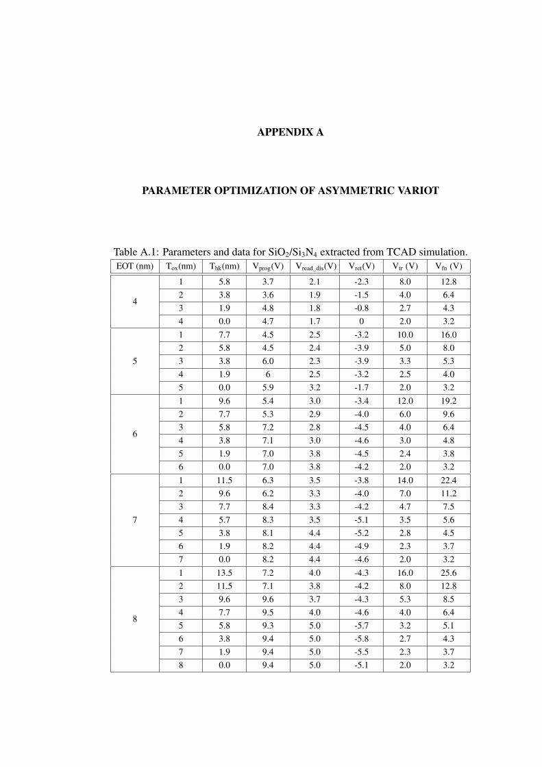
APPENDIX A
PARAMETER OPTIMIZATION OF ASYMMETRIC VARIOT
Table A.1: Parameters and data for SiO2/Si3N4 extracted from TCAD simulation.EOT (nm) Tox(nm) Thk(nm) Vprog(V) Vread_dis(V) Vret(V) Vtr (V) Vfn (V)
4
1 5.8 3.7 2.1 -2.3 8.0 12.82 3.8 3.6 1.9 -1.5 4.0 6.43 1.9 4.8 1.8 -0.8 2.7 4.34 0.0 4.7 1.7 0 2.0 3.2
5
1 7.7 4.5 2.5 -3.2 10.0 16.02 5.8 4.5 2.4 -3.9 5.0 8.03 3.8 6.0 2.3 -3.9 3.3 5.34 1.9 6 2.5 -3.2 2.5 4.05 0.0 5.9 3.2 -1.7 2.0 3.2
6
1 9.6 5.4 3.0 -3.4 12.0 19.22 7.7 5.3 2.9 -4.0 6.0 9.63 5.8 7.2 2.8 -4.5 4.0 6.44 3.8 7.1 3.0 -4.6 3.0 4.85 1.9 7.0 3.8 -4.5 2.4 3.86 0.0 7.0 3.8 -4.2 2.0 3.2
7
1 11.5 6.3 3.5 -3.8 14.0 22.42 9.6 6.2 3.3 -4.0 7.0 11.23 7.7 8.4 3.3 -4.2 4.7 7.54 5.7 8.3 3.5 -5.1 3.5 5.65 3.8 8.1 4.4 -5.2 2.8 4.56 1.9 8.2 4.4 -4.9 2.3 3.77 0.0 8.2 4.4 -4.6 2.0 3.2
8
1 13.5 7.2 4.0 -4.3 16.0 25.62 11.5 7.1 3.8 -4.2 8.0 12.83 9.6 9.6 3.7 -4.3 5.3 8.54 7.7 9.5 4.0 -4.6 4.0 6.45 5.8 9.3 5.0 -5.7 3.2 5.16 3.8 9.4 5.0 -5.8 2.7 4.37 1.9 9.4 5.0 -5.5 2.3 3.78 0.0 9.4 5.0 -5.1 2.0 3.2

173
(a) (b)
(c) (d)
(e)
Figure A.1: Jg − Vg characteristics of SiO2/Si3N4 for EOT (a) 4nm (b) 5nm (c) 6nm(d) 7nm and (e) 8nm.
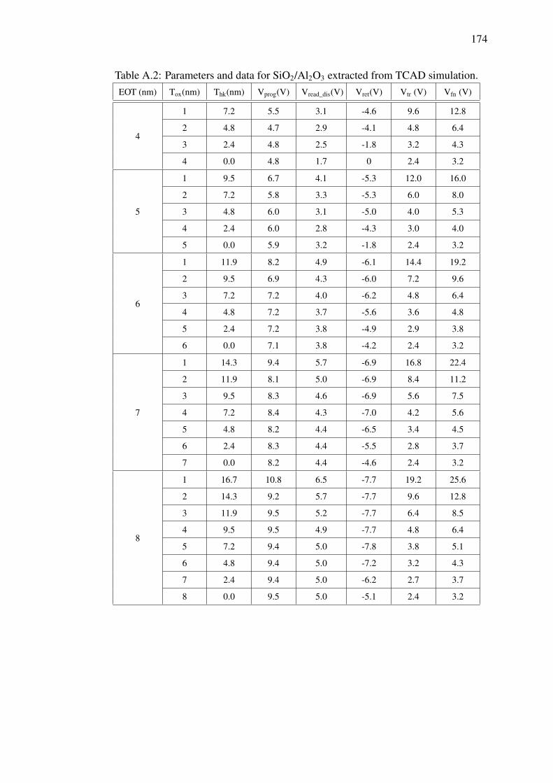
174
Table A.2: Parameters and data for SiO2/Al2O3 extracted from TCAD simulation.EOT (nm) Tox(nm) Thk(nm) Vprog(V) Vread_dis(V) Vret(V) Vtr (V) Vfn (V)
4
1 7.2 5.5 3.1 -4.6 9.6 12.8
2 4.8 4.7 2.9 -4.1 4.8 6.4
3 2.4 4.8 2.5 -1.8 3.2 4.3
4 0.0 4.8 1.7 0 2.4 3.2
5
1 9.5 6.7 4.1 -5.3 12.0 16.0
2 7.2 5.8 3.3 -5.3 6.0 8.0
3 4.8 6.0 3.1 -5.0 4.0 5.3
4 2.4 6.0 2.8 -4.3 3.0 4.0
5 0.0 5.9 3.2 -1.8 2.4 3.2
6
1 11.9 8.2 4.9 -6.1 14.4 19.2
2 9.5 6.9 4.3 -6.0 7.2 9.6
3 7.2 7.2 4.0 -6.2 4.8 6.4
4 4.8 7.2 3.7 -5.6 3.6 4.8
5 2.4 7.2 3.8 -4.9 2.9 3.8
6 0.0 7.1 3.8 -4.2 2.4 3.2
7
1 14.3 9.4 5.7 -6.9 16.8 22.4
2 11.9 8.1 5.0 -6.9 8.4 11.2
3 9.5 8.3 4.6 -6.9 5.6 7.5
4 7.2 8.4 4.3 -7.0 4.2 5.6
5 4.8 8.2 4.4 -6.5 3.4 4.5
6 2.4 8.3 4.4 -5.5 2.8 3.7
7 0.0 8.2 4.4 -4.6 2.4 3.2
8
1 16.7 10.8 6.5 -7.7 19.2 25.6
2 14.3 9.2 5.7 -7.7 9.6 12.8
3 11.9 9.5 5.2 -7.7 6.4 8.5
4 9.5 9.5 4.9 -7.7 4.8 6.4
5 7.2 9.4 5.0 -7.8 3.8 5.1
6 4.8 9.4 5.0 -7.2 3.2 4.3
7 2.4 9.4 5.0 -6.2 2.7 3.7
8 0.0 9.5 5.0 -5.1 2.4 3.2
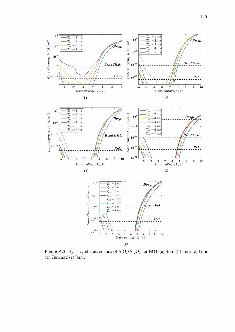
175
(a) (b)
(c) (d)
(e)
Figure A.2: Jg − Vg characteristics of SiO2/Al2O3 for EOT (a) 4nm (b) 5nm (c) 6nm(d) 7nm and (e) 8nm.

176
Table A.3: Parameters and data for SiO2/HfO2 extracted from TCAD simulation.EOT (nm) Tox(nm) Thk(nm) Vprog(V) Vread_dis(V) Vret(V) Vtr (V) Vfn (V)
4
1 14.6 3.0 1.7 -2.2 6.0 12.8
2 9.7 2.8 1.5 -3.5 3.0 6.4
3 4.9 4.9 1.5 -3.1 2.0 4.3
4 0.0 4.8 1.7 0.0 1.5 3.2
5
1 19.5 3.8 2.1 -2.7 7.5 16.0
2 14.6 3.5 1.8 -3.5 3.8 8.0
3 9.7 6.4 1.8 -4.1 2.5 5.3
4 4.9 6.3 2.2 -4.5 1.9 4.0
5 0.0 5.9 3.2 -1.7 1.5 3.2
6
1 24.4 4.5 2.5 -3.2 9.0 19.2
2 19.5 4.2 2.2 -3.5 4.5 9.6
3 14.6 7.5 2.2 -3.7 3.0 6.4
4 9.7 7.3 2.7 -4.8 2.3 4.8
5 4.9 7.0 3.9 -4.9 1.8 3.8
6 0.0 7.0 3.8 -4.1 1.5 3.2
7
1 29.2 5.2 2.9 -3.5 10.5 22.4
2 24.4 5.0 2.6 -3.6 5.3 11.2
3 19.5 8.7 2.5 -4.0 3.5 7.5
4 14.6 8.4 3.1 -4.4 2.6 5.6
5 9.7 8.0 4.5 -5.4 2.1 4.5
6 4.9 8.2 4.4 -5.6 1.8 3.7
7 0.0 8.2 4.4 -4.6 1.5 3.2
8
1 34.1 5.9 3.3 -3.9 12.0 25.6
2 29.2 5.6 2.9 -3.9 6.0 12.8
3 24.4 9.9 2.9 -3.9 4.0 8.5
4 19.5 9.6 3.5 -4.5 3.0 6.4
5 14.6 9.2 5.0 -5.1 2.4 5.1
6 9.7 9.2 5./0 -6.0 2.0 4.3
7 4.9 9.5 5.0 -6.6 1.7 3.7
8 0.0 9.4 5.0 -5.2 1.5 3.2

177
(a) (b)
(c) (d)
(e)
Figure A.3: Jg − Vg characteristics of SiO2/HfO2 for EOT (a) 4nm (b) 5nm (c) 6nm(d) 7nm and (e) 8nm.

178
Table A.4: Parameters and data for SiO2/ZrO2 extracted from TCAD simulation.EOT (nm) Tox(nm) Thk(nm) Vprog(V) Vread_dis(V) Vret(V) Vtr (V) Vfn (V)
4
1 19.2 3.0 1.7 -2.6 5.6 12.8
2 12.8 2.8 1.4 -3.5 2.8 6.4
3 6.4 4.9 1.4 -4.0 1.9 4.3
4 0.0 4.8 1.7 0.0 1.4 3.2
5
1 25.4 3.7 2.1 -3.2 7.0 16.0
2 19.2 3.4 1.8 -3.8 3.5 8.0
3 12.8 6.2 1.7 -4.4 2.3 5.3
4 6.4 6.1 2.2 -4.8 1.8 4.0
5 0.0 5.9 3.2 -1.7 1.4 3.2
6
1 32.1 4.5 2.5 -3.6 8.4 19.2
2 25.6 4.1 2.1 -3.9 4.2 9.6
3 19.2 7.2 2.1 -4.4 2.8 6.4
4 12.8 7.3 2.6 -5.0 2.1 4.8
5 6.4 7.1 3.8 -5.5 1.7 3.8
6 0.0 7.2 3.8 -4.1 1.4 3.2
7
1 38.5 5.2 2.9 -4.0 9.8 22.4
2 32.1 4.8 2.5 -4.0 4.9 11.2
3 25.6 8.5 2.4 -4.3 3.3 7.5
4 19.2 8.4 3.1 -4.9 2.5 5.6
5 12.8 8.2 4.5 -5.3 2.0 4.5
6 6.4 8.3 4.4 -6.2 1.6 3.7
7 0.0 8.2 4.4 -4.6 1.4 3.2
8
1 44.9 5.7 3.3 -4.4 11.2 25.6
2 38.5 5.4 2.8 -4.4 5.6 12.8
3 32.1 9.8 2.7 -4.4 3.7 8.5
4 25.6 9.6 3.5 -4.9 2.8 6.4
5 19.2 9.4 5.1 -5.4 2.2 5.1
6 12.8 9.4 5.0 -6.2 1.9 4.3
7 6.4 9.4 5.0 -7.0 1.6 3.7
8 0.0 9.4 5.0 -5.1 1.4 3.2

179
(a) (b)
(c) (d)
(e)
Figure A.4: Jg−Vg characteristics of SiO2/ZrO2 for EOT (a) 4nm (b) 5nm (c) 6nm (d)7nm and (e) 8nm.

180
(a)
(b) (c)
Figure A.5: (a) JV characteristics for the optimized parameters of all asymmetricVARIOTs conducted. F-N plot of all asymmetric VARIOTs conducted for (b)programming and (c) erase operations.

APPENDIX B
DERIVATION OF CHARGE-BASED COMPACT MODEL
B.1 Charge-Based Compact Model for Partially-Depleted GAANWFETs
Derivation for UCCM Expression;
Poisson’s equation in 1-D for a semiconductor system given as
∇2φ = − ρ
εsi= −
q(p− n+N+
D −N−A
)εsi
(B.1)
1
r
d
dr
(rdφ (r)
dr
)=qNA
εsi
(1 + exp
(φ (r)− 2φf − V
φt
))(B.2)
rdφ (r)
dr=qNAr
2
2εsi+
ˆ r
0
(qNA
εsiexp
(φ0 − 2φf − V
φt
))r · dr (B.3)
given the boundary condition in GAANWFET as
dφ
dr
∣∣∣r=0
= 0, φ (r = 0) = φ0, φ (r = R) = φs (B.4)
The Poisson has no analytical solution due to potential being dependence to r. Inorder to integrate the expression, Following [26], it need to be initially solved for weak

182
inversion and fully-depleted case before latter the moderate and the strong inversionare included. In weak inversion the potential at the surface and the center body is same(φ0 = φs), similar goes to its carrier concentration (n0 = ns).
1
r
d
dr
(rdφ (r)
dr
)=qNA
εsi
(1 + exp
(φ0 − 2φf − V
φt
))(B.5)
Perform the 1st integral for any value of r
rdφ (r)
dr=
ˆ r
0
qNA
εsi
(1 + exp
(φ0 − 2φf − V
φt
))r · dr (B.6)
dφ (r)
dr=qNAr
2εsi+qn0r
2εsi(B.7)
Multiply with R/R
dφ (r)
dr=
(qNAR
2Rεsi+qn0R
2Rεsi
)· r (B.8)
By replacing Qdep = qNAR/2 and Qm = qn0R/2
dφ (r) =
(Qdep +Qm
Rεsi
)r · dr (B.9)
Replace r · dr into Poisson equation without the weak inversion assumption
rdφ (r)
dr=qNAr
2
2εsi+
ˆ φ
φ0
(qNA
εsiexp
(φ (r)− 2φf − V
φt
))(Rεsi
Qdep +Qm
)· dφ (r)
(B.10)

183
Solve for RHS from φ (r = 0) = φ0 to φ (r = r) = φ and using the boundary conditionof dφ
dr
∣∣∣r=R
= −Es , the Poisson can be obtained as
dφ
dr
∣∣∣r=R
=Qdep
εsi+φtR
(2Qdep
Qdep +Qm
)(1− exp
(φ0 − φsφt
))× exp
(φs − 2φf − V
φt
)(B.11)
The second term is actually the total mobile charge, Qm at the channel interface
Qm
εsi=φtR
(2Qdep
Qdep +Qm
)(1− exp
(φ0 − φsφt
))· exp
(φs − 2φf − V
φt
)(B.12)
Using full-depletion approximation of (φ0 − φs) /φt = qNAR2/4εsi. Taking logarithm
to both side and solve for φs
φs = 2φf + V + φt ln
(R
2φtεsi
)− φt ln
(1− exp
(−RQdep
2φtεsi
))+φt ln (Qm) + φt ln
(1 +
Qm
Qdep
)(B.13)
However, Qdep in the last term will results in overestimation of the surface potential instrong inversion region due to the weak inversion approximation. Therefore, following[26], parameter Qdep is changed to Coxφt/H .
φs = 2φf + V + φt ln
(R
2φtεsi
)− φt ln
(1− exp
(−RQdep
2φtεsi
))+φt ln (Qm) + φt ln
(1 +H
Qm
Coxφt
)(B.14)

184
Replacing the surface potential expression into Gauss’s law that enclosed across thegate stack
Cox (Vg −∆ϕ− φs) = Qdep +Qm −Qf + qDitφs (B.15)
Vg − Vth −∆Vth − ηV =Qm
Cox+ ηφt ln
(Qm
Q0
)+ ηφt ln
(1 +
Qm
Q0
)(B.16)
where Q0 = Coxφt/H with
Vth = ∆ϕ+ 2ηφf +Qdep
Cox− Qf
Cox− ηφt ln
(4φtεsiQdep
RQ0
)(B.17)
and
∆Vth = −ηφt ln
(1
Q0
)(B.18)
Derivation for partial-depletion conduction;
1
r
d
dr
(rdφ2 (r)
dr
)=qNA
εsi(B.19)
In partial-depletion conduction, the boundary conditions are given as
dφ2 (r = rdep)
dr= 0, φ2 (r = rdep) = 0, φ2 (r = R) = φ2 . (B.20)
Solving for its first derivative

185
1
r
d
dr
(rdφ2 (r)
dr
)(dφ2 (r)
dr
)=qNA
εsi
(dφ2 (r)
dr
)(B.21)
1
r
d
dr
(rdφ2 (r)
dr
)(dφ2 (r)
dr
)=qNA
εsi
(dφ2 (r)
dr
)(B.22)
(dφ2 (r)
dr
)2
=
ˆ R
rdep
qNA
εsi· dφ2 (r) (B.23)
dφ2
dr
∣∣∣r=R
=
√qNA
εsi· φ2 =
√qNA
εsi· φc; (B.24)
Solution for channel charge;
Qch = −2πR
L̂
0
Qm dy = −µ(2πR)2
Ids
Vdˆ
0
Q2m dV (B.25)
Qch = µ(2πR)2
Ids
[Qm
3Cox+ηφtQ
2m
2+ (B.26)
ηφt
(Q2
0 ln (Qm +Q0) +Q2m
2−Q0Qm
)] ∣∣∣∣∣QmL
Qm0
Solution for drain charge;
Qd = −2πR
L̂
0
y
LQm
dy
dQm
dQm (B.27)
from current continuity equation

186
Ids = 2πRµQmdV
dy= 2πRµQm
dV
dQm
· dQm
dy(B.28)
replacing dy/dQm of the current continuity equation into Qd with dV/dQm isdifferentiate from UCCM expression
Qd = −(2πR)2
Ids
L̂
0
y
LQ2m
[− 1
Cox− ηφt
(1
Qm
+1
Qm +Q0
)]dQm (B.29)
the distance along channel y is again obtained from current continuity equation byrearranging it to be in a function of dy as
dy =2πRµ
IdsQm
[− 1
Cox− ηφt
(1
Qm
+1
Qm +Q0
)]· dQm (B.30)
integrating y from 0 to distance of y and Qm from Qm0 to Qm, distance y is obtained
y =2πRµ
Ids
[Q2m −Q2
m0
2Cox+ ηφt
(2 (Qm −Qm0)−Q0 · log
[Qm +Q0
Qm0 +Q0
])](B.31)
replace y into expression Qd
Qd =
QmLˆ
Qm0
−((2πR)3µ2)
I2dsL·
[Q2m
(ηφt
(2(Qm −Qm0)−Q0 log
(Qm +Q0
Q0 +Qm0
))+Q2m −Q2
m0
2Cox
)(ηφt
(1
Qm +Q0
+1
Qm
)+
1
Cox
)]dQ (B.32)
Solution to integration
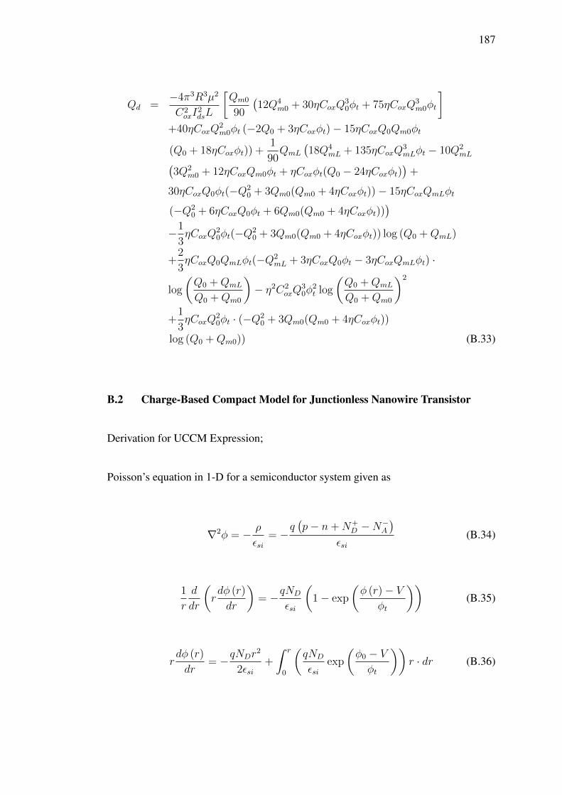
187
Qd =−4π3R3µ2
C2oxI
2dsL
[Qm0
90
(12Q4
m0 + 30ηCoxQ30φt + 75ηCoxQ
3m0φt
]+40ηCoxQ
2m0φt (−2Q0 + 3ηCoxφt)− 15ηCoxQ0Qm0φt
(Q0 + 18ηCoxφt)) +1
90QmL
(18Q4
mL + 135ηCoxQ3mLφt − 10Q2
mL(3Q2
m0 + 12ηCoxQm0φt + ηCoxφt(Q0 − 24ηCoxφt))
+
30ηCoxQ0φt(−Q20 + 3Qm0(Qm0 + 4ηCoxφt))− 15ηCoxQmLφt
(−Q20 + 6ηCoxQ0φt + 6Qm0(Qm0 + 4ηCoxφt))
)−1
3ηCoxQ
20φt(−Q2
0 + 3Qm0(Qm0 + 4ηCoxφt)) log (Q0 +QmL)
+2
3ηCoxQ0QmLφt(−Q2
mL + 3ηCoxQ0φt − 3ηCoxQmLφt) ·
log
(Q0 +QmL
Q0 +Qm0
)− η2C2
oxQ30φ
2t log
(Q0 +QmL
Q0 +Qm0
)2
+1
3ηCoxQ
20φt · (−Q2
0 + 3Qm0(Qm0 + 4ηCoxφt))
log (Q0 +Qm0)) (B.33)
B.2 Charge-Based Compact Model for Junctionless Nanowire Transistor
Derivation for UCCM Expression;
Poisson’s equation in 1-D for a semiconductor system given as
∇2φ = − ρ
εsi= −
q(p− n+N+
D −N−A
)εsi
(B.34)
1
r
d
dr
(rdφ (r)
dr
)= −qND
εsi
(1− exp
(φ (r)− V
φt
))(B.35)
rdφ (r)
dr= −qNDr
2
2εsi+
ˆ r
0
(qND
εsiexp
(φ0 − Vφt
))r · dr (B.36)

188
given the boundary condition in JNT as
dφ
dr
∣∣∣r=0
= 0, φ (r = 0) = φ0, φ (r = R) = φs (B.37)
The Poisson has no analytical solution due to potential being dependence to r. Inorder to integrate the expression, Following [26], it need to be initially solved for weakinversion and fully-depleted case. In weak inversion the potential at the surface andthe center body is same (φ0 = φs), similar goes to its carrier concentration (n0 = ns).
1
r
d
dr
(rdφ (r)
dr
)= −qND
εsi
(1− exp
(φ0 − Vφt
))(B.38)
Perform the 1st integral for any value of r
rdφ (r)
dr=
ˆ r
0
qND
εsi
(−1 + exp
(φ0 − Vφt
))r · dr (B.39)
dφ (r)
dr= −qNAr
2εsi+qn0r
2εsi(B.40)
Multiply with R/R
dφ (r)
dr=
(−qNAR
2Rεsi+qn0R
2Rεsi
)· r (B.41)
By replacing Qdep = qNDR/2 and Qm = qn0R/2
dφ (r) =
(−Qdep +Qm
Rεsi
)r · dr (B.42)

189
Replace r · dr into Poisson equation without the weak inversion assumption
rdφ (r)
dr= −qNDr
2
2εsi+
ˆ φ
φ0
(qND
εsiexp
(φ (r)− V
φt
))(Rεsi
−Qdep +Qm
)· dφ (r)
(B.43)
Solve for RHS from φ (r = 0) = φ0 to φ (r = r) = φ and using the boundary conditionof dφ
dr
∣∣∣r=R
= −Es , the Poisson can be obtained as
dφ
dr
∣∣∣r=R
= −Qdep
εsi+φtR
(2Qdep
−Qdep +Qm
)(1− exp
(φ0 − φsφt
))× exp
(φs − Vφt
)(B.44)
The second term is actually the total mobile charge, Qm at the channel interface
Qm
εsi=φtR
(2Qdep
−Qdep +Qm
)(1− exp
(φ0 − φsφt
))· exp
(φs − Vφt
)(B.45)
The potential relation is replaced by using parabolic potential profile of φ (r) =
(φs − φ0) r2/R2 + φ0, where (φs − φ0) /φt = (−Qdep +Qm) /Qsc. Taking logarithm
to both side and solve for φs
φs = φt ln
(−Qdep +Qm
QdepQsc
)+ φt ln (Qm) + V
−φt ln
(1− exp
[−(−Qdep +Qm
Qsc
)]). (B.46)
Given Gauss’s law at channel interface as

190
Cox (Vg − VFB − ηφs) = −Qdep +Qm (B.47)
where η is the interface trap parameter and by substituting the surface potential intothe Gauss’s law, the UCCM expression for JNT is finally deduced as
Vg−Vth−ηV =Qm
Cox+ηφt ln
(Qm
Qsc
)−ηφt ln
(Qdep [1− exp (−QT/Qsc)]
QT
)(B.48)
The total charge, QT is inferred as −Qdep + Qm and threshold voltage, Vth = VFB −Qdep/Cox.
Solution to drain charge Qd
Qd = QdDP +QdC (B.49)
Qd = −2πR
L̂
0
y
LQDP
dy
dQDP
dQDP − 2πR
L̂
0
y
LQC
dy
dQC
dQC (B.50)
Solution to integration of Equation (5.73)
QdDP = −(QDPL −QDP0)2 (12Q3
DPL + 24Q2DPLQDP0 + 16QDPLQ
2DP0 + 8Q3
DP0)
120Q2eff
−Qeff (QDPL −QDP0)2 (45Q2
DPL + 50QDPLQDP0 + 25Q2DP0)
120QEQ2
−(QDPL −QDP0)2 (40QDPL + 20QDP0)
120(B.51)
Solution to integration of Equation (5.75)

191
QdC = −(QCL −QC0)2 (6Q3
CL + 12Q2CLQC0 + 8QCLQ
2C0 + 4Q3
C0)
60C2Cη
2φ2t
−η (QCL −QC0)2 (45CCφtQ
2CL + 50CCφtQCLQC0 + 25CCφtQ
2C0)
60C2Cη
2φ2t
−(QCL −QC0)2 (80C2
CQCLφ2t + 40C2
CQC0φ2t )
60C2Cφ
2t
(B.52)

APPENDIX C
PUBLICATION LIST
C.1 International Journal
1. Afiq Hamzah, N. Ezaila Alias and Razali Ismail, Low-Voltage High-SpeedProgramming Gate-All-Around Floating Gate (GAA-FG) Memory Cell withTunnel Barrier Engineering, (2018). Japanese Journal of Applied Physics,57(6S3), pp. 06KC02-1–06KC02-8 [Q3, IF=1.384].
2. Afiq Hamzah, M. A. Hilman, N. Ezaila Alias and Razali Ismail, “ScalingChallenges of Floating Gate Non-Volatile Memory and Graphene as theFuture Flash Memory Device: A Review”, Journal of Nanoelectronics andOptoelectronics, (2018) [Q4, IF=0.45]. (Accepted)
3. Afiq Hamzah, Fatimah A. Hamid, and Razali Ismail. (2016). ExplicitContinuous Charge-Based Compact Model for Heavily Doped Surrounding-Gate MOSFETs Incorporating Interface Traps and Fixed Oxide Charges. Journalof Semiconductor and Science Technology, 31(12), pp. 1–13. [Q2, IF=2.13].
C.2 International Conference Proceeding
1. Afiq Hamzah, Zaharah Johari, and Razali Ismail, “A charge-basedcompact modeling of cylindrical surrounding-floating gate MOSFET (S-FGMOSFET) for memory cell application,” in IEEE International Conferenceon Semiconductor Electronics, Proceedings, ICSE, 2016, pp. 157–160.
2. Afiq Hamzah and Razali Ismail, “Performance Prediction of GrapheneNanoribbon and Carbon Nanotube Transistors,” in IEEE InternationalConference on Semiconductor Electronics, Proceedings, ICSE, 2016, pp.149–152.

193
3. Afiq Hamzah, A. Adila Syaidatul, Razali Ismail, and Z. Johari, “PerformanceBenchmarking of Graphene Nanoscroll Transistor with 22nm MOSFET Model,”in Regional Symposium on Micro and Nanoelectronics, 2015, pp. 1–4.