Charge and Exciton Dynamics in Organic Optoelectronic Devices
153
Charge and Exciton Dynamics in Organic Optoelectronic Devices by Caleb Coburn A dissertation submitted in partial fulfillment of the requirements for the degree of Doctor of Philosophy (Physics) in The University of Michigan 2019 Doctoral Committee: Professor Stephen Forrest, Chair Professor Jay Guo Professor Jennifer Ogilvie Associate Professor Kai Sun
Transcript of Charge and Exciton Dynamics in Organic Optoelectronic Devices

Charge and Exciton Dynamics in OrganicOptoelectronic Devices
by
Caleb Coburn
A dissertation submitted in partial fulfillmentof the requirements for the degree of
Doctor of Philosophy(Physics)
in The University of Michigan2019
Doctoral Committee:
Professor Stephen Forrest, ChairProfessor Jay GuoProfessor Jennifer OgilvieAssociate Professor Kai Sun

For Jessie
ii

ACKNOWLEDGEMENTS
It has been said that a dwarf may see further than a giant when standing on its
shoulder. Just as Newton famously attributed his achievements to the giants that
preceded him, so my work would not have been possible alone. In the course of
my graduate work, I’ve had the great pleasure of being introduced to a scientific
community that has both paved the way for my own contributions to the field and
supported me through the journey. Of course, foremost among them is Prof. Stephen
Forrest who mentored and advised me during my graduate school experience. The
example, opportunities, insights, and training he provided shaped my growth as a
scientist. Thank you.
I am also grateful to the senior students who mentored me as a new student:
first Yifan Zhang, who carefully trained me and introduced the rigor that would be
expected of me. I also owe thanks to Michael Slootsky, Kyusang Lee, Xin Xiao,
and especially Jaesang Lee, who worked closely with me on several projects and
mentored my early work on OLEDs. I appreciate the friendship and support of
my contemporaries, including Quinn Burlingame, Yue Qu, Anurag Panda, Xiao Liu,
Xiaozhou Che, Dejiu Fan, Jongchan Kim, and the other students and post docs who
were a part of my graduate experience.
A special mention goes to Eva Ruff. She goes above and beyond as our Admin-
istrative Assistant: she is a friend and support, and assisted with the editing of this
thesis.
iii

Most importantly, I am grateful to my wife, Jessica, who was next to my side
through each step. Her grounding influence has motivated me to work hard and try
to be my best self. Her patience with my long hours in the lab, sympathy when things
didn’t go well, and excitement when they did have made the journey much sweeter.
Also, thanks go to my family, who support me and prepared me to succeed.
iv

TABLE OF CONTENTS
DEDICATION . . . . . . . . . . . . . . . . . . . . . . . . . . . . . . . . . . ii
ACKNOWLEDGEMENTS . . . . . . . . . . . . . . . . . . . . . . . . . . iii
LIST OF FIGURES . . . . . . . . . . . . . . . . . . . . . . . . . . . . . . . viii
LIST OF TABLES . . . . . . . . . . . . . . . . . . . . . . . . . . . . . . . . x
LIST OF ABBREVIATIONS . . . . . . . . . . . . . . . . . . . . . . . . . xi
LIST OF CHEMICALS . . . . . . . . . . . . . . . . . . . . . . . . . . . . xiii
ABSTRACT . . . . . . . . . . . . . . . . . . . . . . . . . . . . . . . . . . . xv
I. Introduction . . . . . . . . . . . . . . . . . . . . . . . . . . . . . . 1
1.1 Introduction to small molecule organic semiconductors . . . . 21.1.1 Organic small molecules . . . . . . . . . . . . . . . . 21.1.2 Energy levels of organic semiconductors . . . . . . . 41.1.3 Charge transport . . . . . . . . . . . . . . . . . . . 61.1.4 Excited states of organic semiconductors . . . . . . 81.1.5 Energy transfer and exciton diffusion . . . . . . . . 101.1.6 Bimolecular annihilation reactions . . . . . . . . . . 12
1.2 Basics of organic light emitting devices . . . . . . . . . . . . . 131.2.1 OLED performance metrics . . . . . . . . . . . . . . 141.2.2 Optics of OLEDs . . . . . . . . . . . . . . . . . . . 181.2.3 OLED characterization . . . . . . . . . . . . . . . . 19
1.3 Organic heterojunctions . . . . . . . . . . . . . . . . . . . . . 201.3.1 Types of organic heterojunctions . . . . . . . . . . . 20
1.4 Charge photogeneration in organic heterojunctions . . . . . . 211.5 Organic photodetector structures . . . . . . . . . . . . . . . . 231.6 Photodetector current-voltage characteristics . . . . . . . . . 24
v
II. Determining polaron and exciton distributions in organic lightemitting devices . . . . . . . . . . . . . . . . . . . . . . . . . . . . 26
2.1 Theory of charge and exciton distributions in a PHOLED . . 272.2 Method of sensitizers . . . . . . . . . . . . . . . . . . . . . . 292.3 Fabrication of devices for measurement of charge balance and
exciton confinement . . . . . . . . . . . . . . . . . . . . . . . 302.4 Measured exciton distribution and device performance . . . . 322.5 Modeling and discussion of results . . . . . . . . . . . . . . . 352.6 Summary . . . . . . . . . . . . . . . . . . . . . . . . . . . . . 41
III. The effect of charge balance and exciton confinement on phos-phorescent organic light emitting device lifetime . . . . . . . . 43
3.1 Measuring charge balance and exciton confinement in PHOLEDs 443.1.1 Requirements for sensing molecules . . . . . . . . . 45
3.2 Fabrication of devices for measurement of charge balance andexciton confinement vs. operating time . . . . . . . . . . . . . 45
3.3 Experimental results . . . . . . . . . . . . . . . . . . . . . . . 483.4 Analysis of charge and exciton leakage . . . . . . . . . . . . . 493.5 Summary . . . . . . . . . . . . . . . . . . . . . . . . . . . . . 54
IV. Stacked white organic light emitting devices for reliable solidstate lighting sources . . . . . . . . . . . . . . . . . . . . . . . . . 57
4.1 Determining the spectrum for a white light source . . . . . . 584.2 The red-green emitting structure . . . . . . . . . . . . . . . . 59
4.2.1 Red-green emitting structure fabrication and opti-mization . . . . . . . . . . . . . . . . . . . . . . . . 60
4.3 The blue emitting structure . . . . . . . . . . . . . . . . . . . 624.4 The charge generation layer . . . . . . . . . . . . . . . . . . . 644.5 Outcoupling considerations . . . . . . . . . . . . . . . . . . . 664.6 Full SWOLED: structure and performance . . . . . . . . . . . 664.7 Analysis of stacked white organic light emitting device (SWOLED)
performance . . . . . . . . . . . . . . . . . . . . . . . . . . . 724.8 Summary . . . . . . . . . . . . . . . . . . . . . . . . . . . . . 73
V. Centimeter-scale electron diffusion in photoactive organic het-erostructures . . . . . . . . . . . . . . . . . . . . . . . . . . . . . . 74
5.1 Device fabrication . . . . . . . . . . . . . . . . . . . . . . . . 755.2 Measurement of lateral photocurrent . . . . . . . . . . . . . . 77
5.2.1 Fitting data with electron diffusion model . . . . . . 795.2.2 Electron diffusion around a cut in the film . . . . . 81
5.3 Frontier orbital energies of HJ and channel materials . . . . . 825.4 Temperature dependent transient photocurrent measurements 845.5 Electrically injected lateral diffusion device . . . . . . . . . . 85
vi
5.6 Analysis of results . . . . . . . . . . . . . . . . . . . . . . . . 875.7 Summary . . . . . . . . . . . . . . . . . . . . . . . . . . . . . 90
VI. Organic charged-coupled devices . . . . . . . . . . . . . . . . . . 92
6.1 Charge manipulation in lateral channels . . . . . . . . . . . . 936.2 Summary . . . . . . . . . . . . . . . . . . . . . . . . . . . . . 108
VII. Future work . . . . . . . . . . . . . . . . . . . . . . . . . . . . . . . 109
7.1 Future work: OLEDs . . . . . . . . . . . . . . . . . . . . . . 1097.1.1 Reliability . . . . . . . . . . . . . . . . . . . . . . . 1097.1.2 Power efficiency . . . . . . . . . . . . . . . . . . . . 1107.1.3 Charge balance and exciton confinement . . . . . . 110
7.2 Future work: OCCDs . . . . . . . . . . . . . . . . . . . . . . 1117.2.1 Controlling background charge density . . . . . . . 1127.2.2 Pixel-scaling . . . . . . . . . . . . . . . . . . . . . . 1137.2.3 Integrated readout circuitry . . . . . . . . . . . . . 1147.2.4 Drift-transport schemes . . . . . . . . . . . . . . . . 1167.2.5 Stacked semitransparent arrays . . . . . . . . . . . . 118
APPENDIX . . . . . . . . . . . . . . . . . . . . . . . . . . . . . . . . . . . . 121
BIBLIOGRAPHY . . . . . . . . . . . . . . . . . . . . . . . . . . . . . . . . 125
vii
LIST OF FIGURES
Figure
1.1 Common simple organic small molecules . . . . . . . . . . . . . . . 31.2 Example molecules used in OLED applications . . . . . . . . . . . . 31.3 Organic molecule frontier orbitals . . . . . . . . . . . . . . . . . . . 51.4 Potential surfaces for hopping transport . . . . . . . . . . . . . . . . 71.5 Exciton transfer mechanisms . . . . . . . . . . . . . . . . . . . . . . 121.6 OLED structures . . . . . . . . . . . . . . . . . . . . . . . . . . . . 141.7 CIE 1931 color matching functions . . . . . . . . . . . . . . . . . . 161.8 CIE 1931 color space . . . . . . . . . . . . . . . . . . . . . . . . . . 181.9 Optical modes . . . . . . . . . . . . . . . . . . . . . . . . . . . . . . 191.10 Types of organic heterojunctions . . . . . . . . . . . . . . . . . . . . 201.11 Charge generation steps . . . . . . . . . . . . . . . . . . . . . . . . 221.12 Built-in field . . . . . . . . . . . . . . . . . . . . . . . . . . . . . . . 231.13 Organic photodetector structure . . . . . . . . . . . . . . . . . . . . 241.14 Organic photodetector current voltage characteristic . . . . . . . . . 252.1 Structure and energy diagram of PHOLEDs for confinement sensing 312.2 Measured and calculated values for exciton distribution . . . . . . . 332.3 Performance of PHOLEDs for confinement sensing . . . . . . . . . . 352.4 Calculated polaron profiles and electron injection energy barrier re-
duction . . . . . . . . . . . . . . . . . . . . . . . . . . . . . . . . . . 393.1 Structure and performance of PHOLEDs for confinement sensing vs
operating time . . . . . . . . . . . . . . . . . . . . . . . . . . . . . . 473.2 Transport layer sensing device spectra vs. aging time . . . . . . . . 503.3 Percentage of charges and excitons lost to transport layers . . . . . 513.4 Contribution of loss of charge balance and exciton confinement to
PHOLED degradation . . . . . . . . . . . . . . . . . . . . . . . . . 554.1 Single emitter and target white spectra . . . . . . . . . . . . . . . . 594.2 Performance of red-green single element devices . . . . . . . . . . . 614.3 Lifetime of red-green single element devices . . . . . . . . . . . . . . 624.4 Performance of blue single element devices . . . . . . . . . . . . . . 634.5 Lifetime of blue single element devices . . . . . . . . . . . . . . . . 634.6 Schematic operation of a charge generation test device . . . . . . . . 65
viii
4.7 Operating voltage and lifetime of charge generation test devices . . 654.8 Outcoupling efficiency vs emission position for selected visible wave-
lengths . . . . . . . . . . . . . . . . . . . . . . . . . . . . . . . . . . 674.9 Full structure of stacked white OLED devices . . . . . . . . . . . . 674.10 SWOLED J–V and efficiency characteristics . . . . . . . . . . . . . 684.11 Spectral characteristics of the SWOLEDs . . . . . . . . . . . . . . . 704.12 Lifetime characteristics of the SWOLEDs . . . . . . . . . . . . . . . 715.1 Device structure, experimental setup, and distance dependent pho-
tocurrent . . . . . . . . . . . . . . . . . . . . . . . . . . . . . . . . . 765.2 Impact of channel disruption on channel currents . . . . . . . . . . 825.3 Energetics of materials employed in devices . . . . . . . . . . . . . . 835.4 Temperature dependence of channel currents . . . . . . . . . . . . . 865.5 Electron diffusion in an electrical injection device . . . . . . . . . . 886.1 Single pixel device dimensions . . . . . . . . . . . . . . . . . . . . . 946.2 Lateral charge confinement device structure and performance. . . . 956.3 Charge collection efficiency versus pulse length . . . . . . . . . . . . 966.4 Background charge transients . . . . . . . . . . . . . . . . . . . . . 976.5 Positive charge accumulation . . . . . . . . . . . . . . . . . . . . . . 986.6 Light and dark pixel transients . . . . . . . . . . . . . . . . . . . . . 1006.7 OCCD mask dimensions . . . . . . . . . . . . . . . . . . . . . . . . 1026.8 OCCD Structure and device photograph . . . . . . . . . . . . . . . 1036.9 OCCD readout scheme and signal . . . . . . . . . . . . . . . . . . . 1046.10 Simulated charge transfer time versus pixel dimension . . . . . . . . 1077.1 Proposed high power efficiency white OLED energy level diagram . 1117.2 Diagram of OCCD electrodes . . . . . . . . . . . . . . . . . . . . . 1137.3 Charge packet integrity vs number of transfers . . . . . . . . . . . . 1147.4 Readout amplifiers styles . . . . . . . . . . . . . . . . . . . . . . . . 1157.5 Thick insulator scheme . . . . . . . . . . . . . . . . . . . . . . . . . 1177.6 Many electrode scheme . . . . . . . . . . . . . . . . . . . . . . . . . 1187.7 Resistive-sheet electrode scheme . . . . . . . . . . . . . . . . . . . . 1197.8 Stacked semitransparent OCCD diagram . . . . . . . . . . . . . . . 120
ix

LIST OF TABLES
Table
2.1 Charge transport parameters used in model fits . . . . . . . . . . . 364.1 Performance characteristics of SWOLEDs . . . . . . . . . . . . . . . 695.1 Room temperature charge diffusion parameters extracted from distance-
dependent transient current measurements . . . . . . . . . . . . . . 80
x
LIST OF ABBREVIATIONS
ALD atomic layer deposition
CCD charge-coupled device
CCT correlated color temperature
CGL charge generation layer
CRI color rendering index
DFT density functional theory
EBL electron blocking layer
EIL electron injection layer
EL electroluminescence
EML emission layer
EQE external quantum efficiency
ETL electron transport layer
FWHM full width at half maximum
HBL hole blocking layer
HJ heterojunction
HIL hole injection layer
HOMO highest occupied molecular orbital
HTL hole transport layer
IMF index matching fluid
IPES inverse photoelectron spectroscopy
xi

IQE internal quantum efficiency
ISC intersystem crossing
J–V current density–voltage
LCD liquid crystal display
LED light emitting diode
LPE luminous power efficiency
LUMO lowest unoccupied molecular orbital
MOS metal-oxide-semiconductor
OCCD organic charge-coupled device
OLED organic light emitting diode
OPV organic photovoltaic
PHOLED phosphorescent organic light emitting device
PLQY photoluminescence quantum yield
PV photovoltaic
SSL solid-state lighting
SWOLED stacked white organic light emitting device
STA singlet-triplet annihilation
TIR total internal reflection
TPA triplet-polaron annihilation
TTA triplet-triplet annihilation
UPS ultraviolet photoelectron spectroscopy
VTE vacuum thermal evaporation
xii

LIST OF CHEMICALS
Alq3 tris-(8-hydroxyquinoline)aluminum
BAlq bis(8-hydroxy-2-methylquinoline)-(4-phenylphenoxy)aluminum
BPhen bathophenanthroline
BPyTP2 2,7-bis(2,20-bipyridine-5-yl)triphenylene
C60 fullerene carbon-60
C70 fullerene carbon-70
CBP 4,4’-bis(9-carbazolyl)-1,1’-biphenyl
CPD di(phenyl-carbazole)-N,N’-bis-phenyl-(1,1’-biphenyl)-4,4’-diamine
CZSi 9-(4-tert-butylphenyl)-3,6-bis(triphenylsilyl)-9H-carbazole
DBP tetraphenyldibenzoperiflanthene
DCM2 4-(dicyanomethylene)-2-methyl-6-julolidyl-9-enyl-4H -pyran
DTDCPB 2-[(7-(4-[N,N -bis(4-methylphenyl)amino]phenyl)-2,1,3-benzothia-diazol-4-yl)methylene]propane-dinitrile
DTDCTB 2-((7-(5-(dip-tolylamino)thiophen-2-yl)benzo[c][1,2,5]thiadiazol-4-yl)methylene)malononitrile
FIrpic bis[2-(4,6-difluorophenyl)pyridinato-C2,N](picolinato)iridium(III)
HATCN hexaazatriphenylene hexacarbonitrile
ITO indium tin oxide
Ir(5’-Ph-ppy)3 iridium (III) tris[2-(5’-phenyl)phenylpyridine]
Ir(dmp)3 iridium (III) tris[3-(2,6-dimethylphenyl)-7-methylimidazo[1,2-f] phenan-thridine]
xiii

Ir(ppy)3 tris[2-phenylpyridine]iridium(III)
Liq 8-hydroxyquinolinato lithium
mer-Ir(pmp)3 mer-tris-(N-phenyl, N-methyl-pyridoimidazol-2-yl)iridium (III)
mCBP 4,40-bis(3-methylcarbazol-9-yl)-2,20-biphenyl
NPD N,N’-Di(1-naphthyl)-N,N’-diphenyl-(1,1’-biphenyl)-4,4’-diamine
PQIr iridium (III) bis(2-phenyl quinolyl-N,C20) acetylacetonate
PtOEP Pt (II) octaethylporphine
SubPc boron subphthalocyanine chloride
TPBi 2,2’,2”-(1,3,5-benzenetriyl tris-[1-phenyl-1H-benzimidazole]
Tris-PCz 9,9’-diphenyl-6-(9-phenyl-9H-carbazol-3-yl)-9H,9’H-3,3’-bicarbazole
xiv

ABSTRACT
Organic optoelectronics use carbon-based molecules to interface between light and
electrical signals. The operation of these devices is determined by the dynamic be-
haviors of their charges and excited states. For example, organic light-emitting diodes
use injected electrical charges to form excited states that, in turn, emit light. Organic
photovoltaics and photodetectors operate by the reverse process. Understanding the
dynamics of charges and excited states is crucial to designing high performance de-
vices.
The first part of this thesis focuses on understanding charge and exciton dynamics
in organic light emitting devices. First, charge balance and exciton confinement in
blue-emitting phosphorescent organic light-emitting diodes are studied using sensi-
tizer methods and an analytical model based on drift-diffusion transport. We find
that triplet excitons leak into the hole transporting layer at high current densities
and improve device performance by incorporating a high triplet energy blocking layer
to prevent such leakage. The impact of changes in charge balance and exciton con-
finement on the lifetime of blue phosphorescent organic light emitting diodes is also
investigated. We find that that contribution of loss of charge balance is negligible,
and that increased exciton leakage is responsible for less than 4% of luminance loss.
The understanding gained in these studies is then applied to the design of a highly
reliable stacked white-emitting device for solid state lighting. These devices employ
xv

red-emitting blocking layers as well as highly stable, low voltage charge generation
layers. A five-stack device achieves 2780 K coordinated color temperature with a high
color rendering index of 89 and 80±20 krs lifetime (T70, 1000 cd/m2).
The second part focuses on charge diffusion in organic heterostructures laterally,
i.e, in plane with the thin film. Because of the low charge mobilities of organic semi-
conductors, organic devices are typically thin with negligible lateral charge transport.
We show that charge can be transported laterally across centimeters in certain organic
heterostructures. This phenomenon arises from the combination of a trap-free, high
diffusivity channel and energetic confinement of carriers that prevents rapid recombi-
nation. The confining energy barrier arises from a polarization shift of the acceptor
material when blended with a highly dipolar donor. Lateral transport heterostruc-
tures are then used to develop the first organic charge-coupled devices. We observe
clear charge-coupled transport of photogenerated charge packets in a linear four-pixel
shift register. Calculations indicate that millisecond readout times are possible us-
ing many-pixel organic charge-coupled sensors, and strategies for the improvement of
these devices are discussed.
xvi
CHAPTER I
Introduction
Organic optoelectronic devices are increasingly prevalent in modern technology.
Among them, organic light emitting diodes (OLEDs) have met with the most com-
mercial success due to their desirable properties for use in information display ap-
plications. Other notable organic optoelectronic devices still in development or in
the early stages of commercialization include organic photovoltaics (OPVs), OLEDs
for solid-state lighting (SSL), thin film transistors, photodetectors, lasers, and more.
Inorganic semiconductors are more commonly used for many of these optoelectronic
device applications, i.e, light emitting diodes (LEDs), photovoltaics (PVs), etc. The
viability of optoelectronic devices based on organic materials depends on the value of
the unique properties of organics to the application in question. For example, amor-
phous organics can achieve efficient light emission that is tunable across the visible
spectrum. This gives OLED displays a large advantage over their inorganic coun-
terparts because of the relative ease of patterning amorphous rather than crystaline
materials into active pixels. This has led to the commercial success of OLED display
technology, which is widely viewed as superior to liquid crystal display (LCD) tech-
nology. The true inorganic analogue to OLED display, dubbed microLED, is still in
development due to the high cost and difficulty of pixel transfer processes.
1

Despite the successful commercialization of OLEDs, there remain some key areas
of research for their improvement. These include efficient light outcoupling, high
power efficiency, and reliability. Outcoupling refers to extracting light from the high-
index organic materials into the air where it is viewed. Power efficiency requires
maximizing the efficiency with which electrical current is converted into light power,
and minimizing the operating voltage to near the thermodynamic limit. Finally,
improving reliability requires understanding the active degradation mechanisms in
device structures. The reliability of blue emitting OLEDs is particularly challenging
due to the high energy excitation required to reach the blue end of the spectrum.
The first half of this thesis addresses advances in OLED technology, with emphasis
on understanding the relationship between charge and exciton dynamics and the
reliability of blue OLEDs.
In addition to enabling useful optoelectronic devices, there is rich science to explore
in the field of organic electronics. Often, improving our understanding of phenomena
observed in organic semiconductor systems in turn enables new applications. The
second part of this thesis focuses on one such phenomenon, long range lateral charge
transport in organic heterostructures, and its application to organic charge-coupled
devices (CCDs).
1.1 Introduction to small molecule organic semiconductors
1.1.1 Organic small molecules
Molecules containing carbon-hydrogen bonds are classified as organic. Small
molecules have low molecular weight and are typically less than 900 atomic mass
units. Organic molecules used in optoelectronic applications are held together by
covalent bonds and often are assembled by joining several organic groups together.
Some examples of these organic groups are shown in Fig. 1.1. It is understood that
2
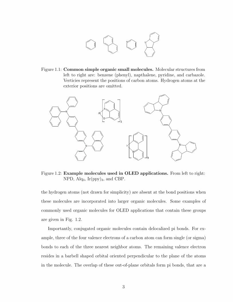
Figure 1.1: Common simple organic small molecules. Molecular structures fromleft to right are: benzene (phenyl), napthalene, pyridine, and carbazole.Verticies represent the positions of carbon atoms. Hydrogen atoms at theexterior positions are omitted.
Figure 1.2: Example molecules used in OLED applications. From left to right:NPD, Alq3, Ir(ppy)3, and CBP.
the hydrogen atoms (not drawn for simplicity) are absent at the bond positions when
these molecules are incorporated into larger organic molecules. Some examples of
commonly used organic molecules for OLED applications that contain these groups
are given in Fig. 1.2.
Importantly, conjugated organic molecules contain delocalized pi bonds. For ex-
ample, three of the four valence electrons of a carbon atom can form single (or sigma)
bonds to each of the three nearest neighbor atoms. The remaining valence electron
resides in a barbell shaped orbital oriented perpendicular to the plane of the atoms
in the molecule. The overlap of these out-of-plane orbitals form pi bonds, that are a
3
result of double bonds between carbon atoms. A classic demonstration of this bond-
ing structure is benzene (see Fig. 1.1). Due to the symmetry of the molecule, the
pi bonds are delocalized over the ring. This forms a conjugation system, or system
of connected, delocalized pi bonds. Electrons can move freely along the conjugation
system (intramolecular conduction), while the overlap of pi bonds between adjacent
molecules also allows for intermolecular conduction.
While organic molecules are held together by covalent bonds, they typically have
closed outer shells and thus do not chemically bond with each other. Rather, or-
ganic solids are made of molecules held together by van der Waals bonds that result
from dipole interactions between molecules. van der Waals bonds are much weaker
(∼meV) than covalent bonds (∼eV). Having strong intramolecular bonds but weak
intermolecular bonds gives rise to many of the properties unique to organic solids.
1.1.2 Energy levels of organic semiconductors
Weak van der Waals bonds lead to poor electronic coupling between organic
molecules. Organic semiconductors therefore only rarely exhibit band like transport,
and then only for highly purified, well-ordered crystals. It follows that amorphous
organics do not have the familiar valence and conduction bands like inorganic semi-
conductors, rather they have molecular energy levels. The energy levels of primary
interest are the highest occupied molecular orbital (HOMO) and lowest unoccupied
molecular orbital (LUMO) levels. As their names suggest, these correspond to the
highest energy level occupied by the electrons of the neutral molecule and the lowest
energy unoccupied level. These energies are typically specified in units of electron
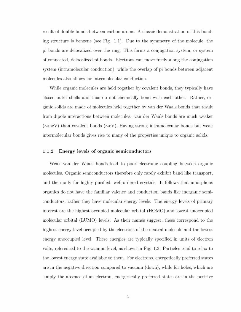
volts, referenced to the vacuum level, as shown in Fig. 1.3. Particles tend to relax to
the lowest energy state available to them. For electrons, energetically preferred states
are in the negative direction compared to vacuum (down), while for holes, which are
simply the absence of an electron, energetically preferred states are in the positive
4
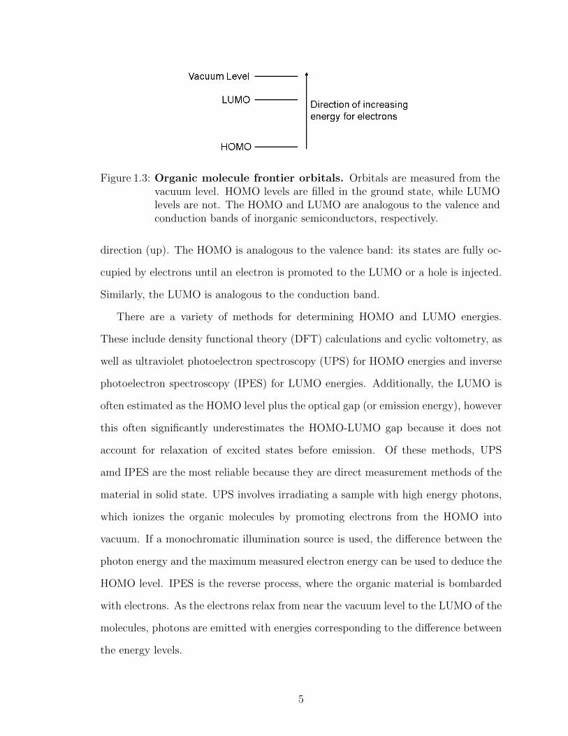
Figure 1.3: Organic molecule frontier orbitals. Orbitals are measured from thevacuum level. HOMO levels are filled in the ground state, while LUMOlevels are not. The HOMO and LUMO are analogous to the valence andconduction bands of inorganic semiconductors, respectively.
direction (up). The HOMO is analogous to the valence band: its states are fully oc-
cupied by electrons until an electron is promoted to the LUMO or a hole is injected.
Similarly, the LUMO is analogous to the conduction band.
There are a variety of methods for determining HOMO and LUMO energies.
These include density functional theory (DFT) calculations and cyclic voltometry, as
well as ultraviolet photoelectron spectroscopy (UPS) for HOMO energies and inverse
photoelectron spectroscopy (IPES) for LUMO energies. Additionally, the LUMO is
often estimated as the HOMO level plus the optical gap (or emission energy), however
this often significantly underestimates the HOMO-LUMO gap because it does not
account for relaxation of excited states before emission. Of these methods, UPS
amd IPES are the most reliable because they are direct measurement methods of the
material in solid state. UPS involves irradiating a sample with high energy photons,
which ionizes the organic molecules by promoting electrons from the HOMO into
vacuum. If a monochromatic illumination source is used, the difference between the
photon energy and the maximum measured electron energy can be used to deduce the
HOMO level. IPES is the reverse process, where the organic material is bombarded
with electrons. As the electrons relax from near the vacuum level to the LUMO of the
molecules, photons are emitted with energies corresponding to the difference between
the energy levels.
5
1.1.3 Charge transport
The electric field from electrons and holes polarizes the molecules surrounding the
charges. This screens the electric field from more distant locations and energetically
stabilizes the charges. Together, the charges and their associated relaxation are re-
ferred to as polarons. Because organic molecules have weak intermolecular bonds and
therefore electronic coupling, charges tend to be localized onto single molecules, and
the transport of polarons occurs in discrete molecule-to-molecule steps, called ‘hop-
ping’ transport. The coupling between molecules improves as the overlap between
their pi orbital systems increases. However, because the polarization of the surround-
ing medium is centered on the electron, the polaron carries with it a small potential
well. The result is that the polaron is ‘sticky,’ i.e, it takes energy to instigate a hop
over the barrier at the edge of the potential. This situation is shown schematically in
Fig. 1.4.
The two parabolas represent the potential surface for an electron on two adjacent
molecules. To hop from one to the other, the electron must overcome the rise in
potential between the two potential minima. This barrier increases as the energy of
the destination site increases relative to its origin. The hopping rate, as described by
Marcus theory, relates to the energy offset via ktransfer ∝ exp[−EB/kBT )], where the
energy barrier EB = (λ− G0)2/(4λ). Here, λ is the height of origin potential at the
position of the destination potential, and G0 is the difference in potential minima.
Because organics are disordered, there is variation in the energy of each site even for
similar molecules due to local variations in molecular orientation and position. Thus,
the microscopic details of hopping transport are complex and usually inaccessible
experimentally. To understand bulk charge transport properties, it is useful to define
bulk properties that describe the average behavior of charges in the solid.
Because applying an electric field makes it energetically favorable for charges to
hop in the direction of the field, it results in the net flow of charges. The mobility, µ,
6

Figure 1.4: Potential surfaces for hopping transport. The two parabolas repre-sent the potential of a charge as it moves between two adjacent molecules.
describes how fast the charges move in response to an applied field via the definition
v = µF , where v is the velocity of the charges and F is the magnitude of the electric
field. The drift current is Jdr = µFn, where n is the carrier density. Additionally,
charges undergo random, thermally driven hopping motion, called diffusion. Because
the diffusion is random, there is a net carrier flux from areas of high charge concen-
tration to areas with low concentration. There is no driving force pushing charges
towards areas of low concentration, rather it arises from purely statistical considera-
tions. Quantitatively, the diffusion current is Jdi = D dndx
, where D is the diffusivity.
In general, the mobility and diffusivity are different for electrons and holes. The
time evolution of a distribution of charges modeled with drift diffusion can then be
described by the partial differential equation:
d
dtn(x, t) = ∇(D(x)∇n(x, t))−∇(µ(x)n(x, t)F (x, t)) (1.1)
together with appropriate boundary conditions.
In many cases the drift-diffusion model is too ideal to adequately describe the
behavior of charges in organic semiconductors, and other effects must be considered.
7
For example, it does not consider the energy barrier between transport sites due
to disorder and lattice polarization. Because hopping transport is often thermally
activated, the transfer rate to a molecule with higher energy than the original position
is decreased. Barrier reduction can be described using Poole-Frenkel theory via the
field-dependent mobility function µ = µ0exp(−√F ).
1.1.4 Excited states of organic semiconductors
Excited states are formed when an electron is promoted to a higher lying energy
level, for example the LUMO. This is commonly done by photon absorption or by
electrical excitation via injection of carriers at conductive contacts. The electron in
the higher lying state is still Coloumbically bound to the positive counter-charge of
the net-neutral molecule. The bound excited state is called an exciton. The binding
energy and how it changes with the distance between charges as well as the dielectric
constant can be understood by the Bohr model which describes the classical energy of
electron orbits. The Bohr model energy is E = e2
8πεr, where e is the electron charge, ε is
the dielectric constant, and r is the distance between the charges. The binding energy
is reduced in high dielectric constant media. This effect is pronounced for inorganic
semiconductors (ε & 10). The binding energy is also reduced because the effective
mass of the charges is small, leading to larger orbitals and average distance between
carriers. Excitons in inorganic semiconductors therefore have smaller binding energies
that are easily overcome by thermal energy at room temperature. The excitons readily
dissociate into free carriers.
This type of exciton, i.e, delocalized and weakly bound, are called Wannier-Mott
excitons. Organic semiconductors, on the other hand, typically have a lower dielectric
constant (≈ 3). Thus the exciton binding energy is high compared to the thermal
energy. Tightly bound, localized excitons are called Frenkel excitons.
8

1.1.4.1 Single and Triplet Excitons
The Pauli exclusion principle states that no two identical Fermions can occupy
the same state on a single molecule, i.e, they must differ by at least one quantum
number. This can be shown to be equivalent to requiring that the total wave function
of electrons in a molecule or atom be antisymmetric under particle exchange. Because
most organic molecules in the ground state have full outer shells, each electron is
paired with an electron that differs only in spin, leading to zero net spin. Zero-spin
two-electron states are called singlet states because there is only one such state, i.e,
1√2(|↑↓〉− |↓↑〉), which is antisymmetric under particle exchange. To satisfy the Pauli
exclusion principle, the spatial component of the wavefunction must be symmetric
under exchange.
If two electrons differ in, for example, the principle quantum number, three spin
wavefunctions with total spin of 1 are possible in addition to the singlet state men-
tioned above. These are: 1√2(|↑↓〉+ |↓↑〉), |↑↑〉, and |↓↓〉, each of which is symmetric
under particle exchange. These are called triplet states. To satisfy the Pauli exclusion
principle, the spatial portion of a triplet state wavefunction must be antisymmetric
with respect to exchange, opposite the spatial symmetry of singlets. This has impor-
tant consequences for photon emission, because radiative transitions cannot couple
wavefunctions with opposite particle exchange symmetries in the spatial wavefunc-
tion. Thus, excited state and ground state singlets are coupled via absorption and
emission, but the ground state singlet can’t be optically excited to a triplet state, nor
a triplet state radiatively relax into the ground state.
Emission from excited singlet states is called fluorescence, and typically has a
radiative rate ∼109 s-1. Phosphorescence, which refers to emission from excited triplet
states, would not be possible without mixing singlet and triplet states. Perturbations
to the potential, such as spin-orbit coupling, cause some state mixing. This means
that triplet states acquire some singlet character, causing absorption and emission
9

to become weakly allowed. For organic molecules composed entirely of light atoms
such as pure hydrocarbons, the resulting radiative rate is slow, typically 100−103 s-1.
However, the magnitude of spin-orbit coupling scales as the atomic number to the
fourth power. Thus incorporating heavy elements, such as Ir and Pt, can dramatically
increase the radiative rate, with some phosphorescent compounds reaching ∼106 s-1.
Before they relax due to radiative or nonradiative processes, excitons may diffuse in
the organic material.
While photon absorption primarily results in singlet excitons, both singlets and
triplets can be stimulated by current injection. Because the spins of injected carriers
are uncorrelated, electrical excitation is statistically expected to yield one singlet for
every three triplets, following the multiplicity of the states [1]. Thus, the theoreti-
cal maximum internal quantum efficiency (IQE) of fluorescent devices is expected
to be ∼25% (not considering annihilation effects, which are discussed later). In a
phosphorescent device, the maximum attainable IQE reaches 100% [2].
1.1.5 Energy transfer and exciton diffusion
Exciton diffusion occurs primarily by Forster [3] or Dexter [4] energy transfer. Forster
transfer (often referred to as Forster resonance energy transfer, or FRET) is a non-
radiative process by which excitons are transferred between molecules through dipole-
dipole interactions. Because dipole field strength varies as r−3 and Forster transfer
results from the interaction of two dipoles, Forster transfer rate scales as r−6. Specif-
ically, the transfer efficiency is 11+(r/r0)6
, where r0 is the Forster radius, or 50 percent
transfer efficiency distance. The Forster radius is calculated as
r60 =
9κ2Φ
128π5n4
∫φ(λ)σ(λ)λ4dλ. (1.2)
Here, κ2 is the dipole orientation factor, Φ is the quantum yield of the donor, n
is the index of refraction, φ is the emission spectrum (normalized to area), and σ is
10

the attenuation cross section of the acceptor. For isotropic dipole orientation, κ =
2/3. Thus, Forster transfer becomes more efficient over smaller distances and with
increased overlap of the absorption and emission spectra of the molecules. Typical
Forster radii are less than 10 nm. The same selection rules that disallow triplet
absorption and emission also disallow Forster transfer, however it is accessible by
triplets on phosphorescent molecules due to singlet state mixing, and between two
excited triplet states.
Dexter transfer, in contrast, results from the coincident hopping of electrons be-
tween neighboring excited and ground state molecules. As such, it is shorter range
than Forster transfer. The Dexter transfer rate depends on the overlap of emission
and absorption spectra, the distance between sites, and the details of the wavefunc-
tions and exchange Hamiltonian [4]. The rate scales approximately with separation
as
kdexter ∝ Jexp(−2r
L), (1.3)
where J is the overlap integral of the emission spectrum of the donor with the ab-
sorption spectrum of the acceptor, r is the distance between donor and acceptor, and
L is an effective average radius of the excited and ground states involved. Dexter
transfer is not restricted by dipole transition selection rules. It only requires that
spin be conserved during transfer. Thus, triplet states are free to transfer via the
Dexter mechanism to adjacent ground state singlet molecules.
These mechanisms are represented schematically in Fig. 1.5. Triplet Forster
transfer and singlet Dexter transfer are also possible, but tend to be dominated by
triplet Dexter transfer and singlet Forster transfer, respectively.
11

Figure 1.5: Exciton transfer mechanisms. (Top) Schematic representation ofsinglet-singlet Forster transfer. (Bottom) Schematic representation oftriplet-singlet Dexter transfer. 1S is the first (lowest energy) singlet ex-cited state, 0S is the ground singlet state, and 1T is the first triplet state.
1.1.6 Bimolecular annihilation reactions
At high excitation densities, there can be annihilation reactions caused by excited
state reactions. The most common of these in phosphorescent devices involve triplets,
primarily triplet-triplet annihilation (TTA) and triplet-polaron annihilation (TPA).
In fluorescent devices, including organic lasers, singlet-triplet annihilation (STA) plays
an important role.
TTA occurs when triplet excitons interact, possibly by diffusing to the same
molecule. This results in the relaxation of one exciton and further excitation of
the other, creating a hot state. This is followed by rapid thermalization of the hot
excited state to the first excited state. An example of a TTA reaction is
T1 + T1 → Sn + S0 → S1 + S0 (1.4)
where 1T is the first (lowest energy) triplet excited state, Sn is a multiply excited
singlet state, S1 is the first singlet state, and S0 is the ground state. TPA proceeds
similarly, with a polaron and triplet reacting, resulting in a ground state molecule
12
and a hot polaron that quickly relaxes back down to the transport level. Because
they result in the net loss of an exciton, these annihilation reactions are a channel for
energy and efficiency loss. The annihilation rate increases with the excitation density
as kTTT2 and kTPnT for TTA and TPA, respectively, where kTT and kTP are rate
constants, T is the triplet density, and n is the polaron density. The rate constants
are proportional to the sum of the diffusivities of the participating particles, i.e,
annihilation is more severe for larger diffusivities. As they are quadratic in the particle
densities, these effects are most pronounced at high intensity. This causes efficiency
roll-off in phosphorescent OLEDs [5] as well as accelerating intrinsic degradation in
blue phosphorescent organic light emitting devices (PHOLEDs) [6] due to resultant
hot states causing bond rupture of the molecules.
1.2 Basics of organic light emitting devices
In its simplest form, an OLED comprises a single layer of organic material sand-
wiched between two contacts. When the contacts are biased, electrical carriers are
injected, holes from the anode and electrons from the cathode. These can recombine
in the organic layer, forming excitons which may emit light. If one or more of the
electrodes is transparent, some of the generated light will be emitted out of the de-
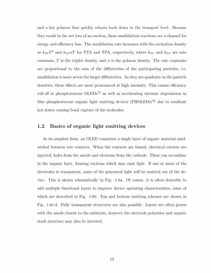
vice. This is shown schematically in Fig. 1.6a. Of course, it is often desirable to
add multiple functional layers to improve device operating characteristics, some of
which are described in Fig. 1.6b. Top and bottom emitting schemes are shown in
Fig. 1.6c-d. Fully transparent structures are also possible. Layers are often grown
with the anode closest to the substrate, however the electrode polarities and organic
stack structure may also be inverted.
13
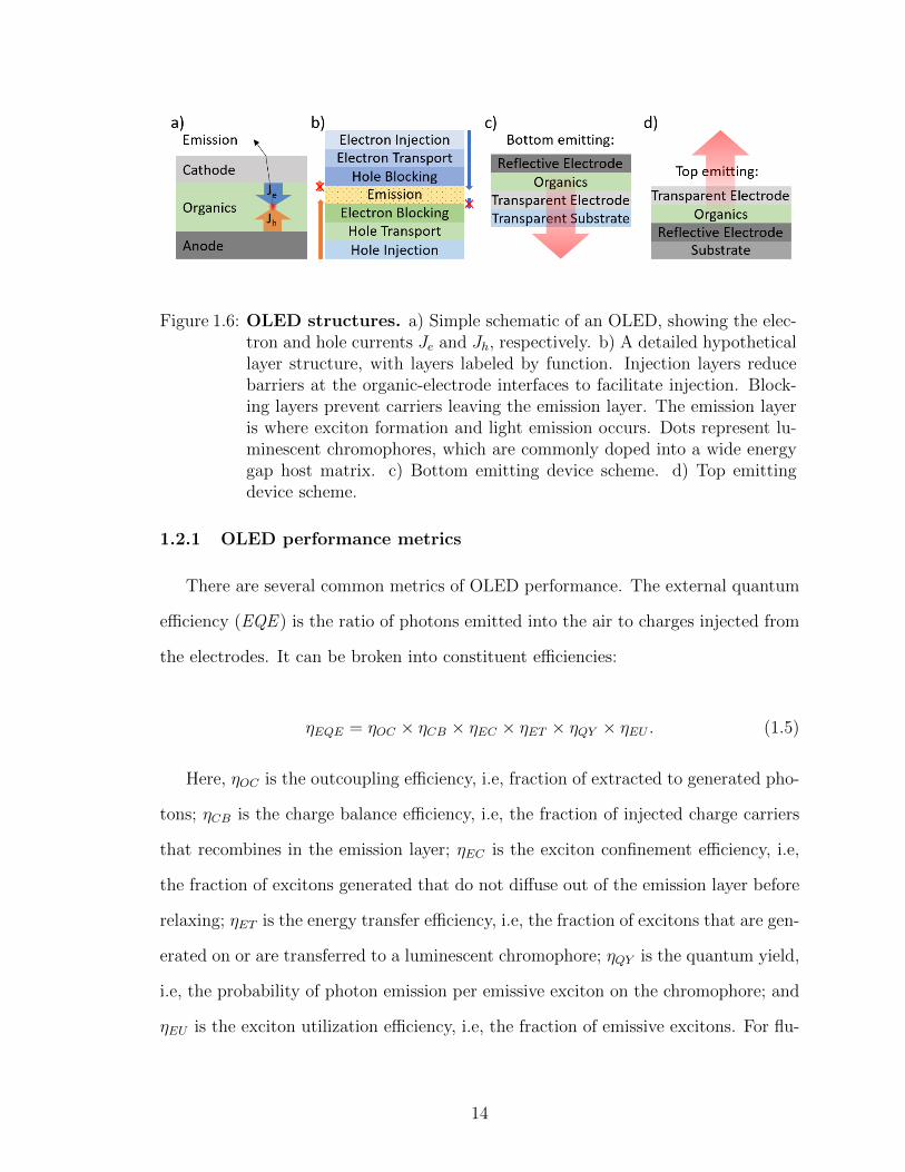
Figure 1.6: OLED structures. a) Simple schematic of an OLED, showing the elec-tron and hole currents Je and Jh, respectively. b) A detailed hypotheticallayer structure, with layers labeled by function. Injection layers reducebarriers at the organic-electrode interfaces to facilitate injection. Block-ing layers prevent carriers leaving the emission layer. The emission layeris where exciton formation and light emission occurs. Dots represent lu-minescent chromophores, which are commonly doped into a wide energygap host matrix. c) Bottom emitting device scheme. d) Top emittingdevice scheme.
1.2.1 OLED performance metrics
There are several common metrics of OLED performance. The external quantum
efficiency (EQE ) is the ratio of photons emitted into the air to charges injected from
the electrodes. It can be broken into constituent efficiencies:
ηEQE = ηOC × ηCB × ηEC × ηET × ηQY × ηEU . (1.5)
Here, ηOC is the outcoupling efficiency, i.e, fraction of extracted to generated pho-
tons; ηCB is the charge balance efficiency, i.e, the fraction of injected charge carriers
that recombines in the emission layer; ηEC is the exciton confinement efficiency, i.e,
the fraction of excitons generated that do not diffuse out of the emission layer before
relaxing; ηET is the energy transfer efficiency, i.e, the fraction of excitons that are gen-
erated on or are transferred to a luminescent chromophore; ηQY is the quantum yield,
i.e, the probability of photon emission per emissive exciton on the chromophore; and
ηEU is the exciton utilization efficiency, i.e, the fraction of emissive excitons. For flu-
14

orescent devices, ηEU is the singlet yield. Bottom emitting devices using a top metal
cathode and glass substrate (index ∼1.5) have a maximum outcoupling efficiency
of about 20% [7], which can be enhanced significantly by employing light-extraction
structures [8–11]. For well-designed devices, near unity ηCB and ηEC are achievable.
This largely depends on the energetics of the confinement layers and position of the
exciton formation zone, which is determined by the details of carrier transport. For
appropriate doping concentrations employing a host-dopant pair with efficient host-
to-guest energy transfer (by Forster or Dexter mechanisms), ηET can also approach
unity. The quantum yield is a property of the chromophore, arising from details of its
chemical structure. Finally, ηEU is often considered to be 0.25 for fluorescent devices
due to the singlet yield, however this neglects TTA and other sources of delayed emis-
sion such as back transfer from singlet to triplet states. For phosphorescent devices,
ηEU = 1. Removing ηOC from the right hand side of Eq. 1.5 yields the IQE.
Power conversion efficiency, ηPCE, is the ratio of optical output power to electrical
input power, which is 100% if the device operating voltage corresponded to the photon
energy (in eV) and EQE = 100%. In practice, this is difficult to achieve even for
devices with IQE = 100% due to losses in outcoupling as well as resistive losses and
relaxation of the exciton, causing the emission energy to be less than the HOMO-
LUMO gap. For a green bottom emitting device with no outcoupling scheme, 100%
IQE, and operating voltage of 7 V (∼3× the photon energy), ηPCE ≈ 6%.
Additional efficiency metrics that are important for evaluating devices intended for
display or illumination require an understanding of human color perception. Stan-
dards for human color and luminosity perception were defined in 1931 by the In-
ternational Commission on Illumination based on the experiments of Wright and
Guild [12,13]. The standards are based on the response functions of the three types
of cone cells that our eyes use to distinguish color, known as the color matching
functions. The three color matching functions are plotted in Fig. 1.7.
15
Figure 1.7: CIE 1931 color matching functions.
The Y color matching function, which peaks at 555 nm, is also known as the
photopic response curve, which describes how we perceive brightness. In this context
it is defined to be 683 lumens per watt (lm/W) at its maximum. Thus, emission
spectra with high intensity in the green appear brighter than spectra with equal
optical intensity but centered in the red, blue, or outside of the visible spectrum.
Quantitatively, the responsivity of the eye, Φ, to an arbitrary spectrum is
Φ = 683
∫φ(λ)Y (λ)dλ, (1.6)
where φ(λ) is the input spectrum, normalized to unit area. We can now define the
luminous power efficiency (LPE), which is simply ηLPE = ΦηPCE, and describes the
luminous flux output per unit power input.
Another quantity of interest, especially for describing a display, is the luminance,
measured in cd/m2. Luminance describes the luminous intensity per area as ob-
served from a given direction, which is a measure of the apparent brightness of the
source observed directly (as opposed to luminous flux, which is a measure of the total
illumination output of a source). Quantitatively, luminance is
16

LV =d2ΦL(θ)
dAdΩcos(θ), (1.7)
where ΦL(θ) is the luminous flux emitted from area dA into solid angle dΩ, and θ is the
angle between surface normal and the emission direction. For a lambertian emitter
radiating into a 2π sr half-space, i.e, the special case for which ΦL(θ) = ΦL,maxcos(θ),
the luminance is constant and is related to the luminous flux per area by 1 cd/m2 = π
lm/m2. Yet another performance metric, primarily used for displays, is the luminance
current efficiency, measured in cd/A.
The color matching functions in Fig. 1.7 are used to quantify the color of a
spectrum. First, the spectrum is integrated against the three color matching functions
to obtain X, Y , and Z:
X =
∫φ(λ)X(λ)dλ,
Y =
∫φ(λ)Y (λ)dλ,
Z =
∫φ(λ)Z(λ)dλ.
The CIE color coordinates are then calculated as:
x =X
X + Y + Z, y =
Y
X + Y + Z(1.8)
with the pair (x, y) indicating the color coordinate on the 1931 CIE color chart, shown
in Fig. 1.8.
For white light sources, the spectrum can be described by its correlated color
temperature (CCT) and color rendering index (CRI). The CCT is the temperature
of the black-body closest to the white light source on the CIE color space, determined
17

Figure 1.8: CIE 1931 color space. Blue numbers labeled around the colorspaceindicate the wavelength in nm for monochromatic spectra.
by the intersection of the line perpendicular to the Plankian locus that also intersects
the (x, y) coordinate of the light source. The CRI describes how similar the spectrum
is to a black-body with the same CCT. It is calculated by averaging the difference
between reflection spectra from a series of standard color samples when illuminated
by the white light source versus the black-body reference spectrum [14].
1.2.2 Optics of OLEDs
The outcoupling efficiency as well as the angular intensity and spectral dependen-
cies, are determined by the optical structure of the device. The optical power trans-
port can be modeled by calculating the emission pattern from point dipoles located
at the position of the excitons. For a conventional bottom emitting device employing
a top metal electrode, there are several available modes into which the optical power
will be coupled. These include air modes, substrate modes, waveguide modes, and
18
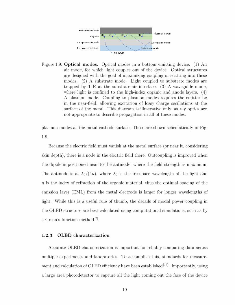
Figure 1.9: Optical modes. Optical modes in a bottom emitting device. (1) Anair mode, for which light couples out of the device. Optical structuresare designed with the goal of maximizing coupling or scatting into thesemodes. (2) A substrate mode. Light coupled to substrate modes aretrapped by TIR at the substrate-air interface. (3) A waveguide mode,where light is confined to the high-index organic and anode layers. (4)A plasmon mode. Coupling to plasmon modes requires the emitter bein the near-field, allowing excitation of lossy charge oscillations at thesurface of the metal. This diagram is illustrative only, as ray optics arenot appropriate to describe propagation in all of these modes.
plasmon modes at the metal cathode surface. These are shown schematically in Fig.
1.9.
Because the electric field must vanish at the metal surface (or near it, considering
skin depth), there is a node in the electric field there. Outcoupling is improved when
the dipole is positioned near to the antinode, where the field strength is maximum.
The antinode is at λ0/(4n), where λ0 is the freespace wavelength of the light and
n is the index of refraction of the organic material, thus the optimal spacing of the
emission layer (EML) from the metal electrode is larger for longer wavelengths of
light. While this is a useful rule of thumb, the details of modal power coupling in
the OLED structure are best calculated using computational simulations, such as by
a Green’s function method [7].
1.2.3 OLED characterization
Accurate OLED characterization is important for reliably comparing data across
multiple experiments and laboratories. To accomplish this, standards for measure-
ment and calculation of OLED efficiency have been established [15]. Importantly, using
a large area photodetector to capture all the light coming out the face of the device
19
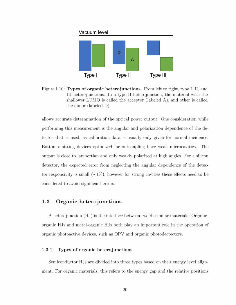
Figure 1.10: Types of organic heterojunctions. From left to right, type I, II, andIII heterojunctions. In a type II heterojunction, the material with theshallower LUMO is called the acceptor (labeled A), and other is calledthe donor (labeled D).
allows accurate determination of the optical power output. One consideration while
performing this measurement is the angular and polarization dependence of the de-
tector that is used, as calibration data is usually only given for normal incidence.
Bottom-emitting devices optimized for outcoupling have weak microcavities. The
output is close to lambertian and only weakly polarized at high angles. For a silicon
detector, the expected error from neglecting the angular dependence of the detec-
tor responsivity is small (∼1%), however for strong cavities these effects need to be
considered to avoid significant errors.
1.3 Organic heterojunctions
A heterojunction (HJ) is the interface between two dissimilar materials. Organic-
organic HJs and metal-organic HJs both play an important role in the operation of
organic photoactive devices, such as OPV and organic photodectectors.
1.3.1 Types of organic heterojunctions
Semiconductor HJs are divided into three types based on their energy level align-
ment. For organic materials, this refers to the energy gap and the relative positions
20
of the HOMO / LUMO values. The three types of HJ are shown in Fig. 1.10. For
a Type I HJs, the HOMO and LUMO of one material lie within the energy gap of
the other. This results in blocking behavior for charges and excitons on the smaller
energy gap material and exothermic transfer across the HJ for those on the wide en-
ergy gap material. Type II HJs have staggered energy gaps, such that transfer across
the interface is exothermic for holes in one direction and for electrons in the opposite
direction, and can facilitate charge separation of excitons. The materials in a type II
HJ are called donors and acceptors, according to the direction of electron transfer, i.e,
the material with the deeper LUMO is the acceptor. Type III HJs involve materials
without any overlap in the energy gaps.
The energy levels of the individual materials may shift from their bulk values
at the HJ due to the formation of interface dipoles, charge transfer, polarization,
or dielectric effects [16]. The energy shifts can be investigated using UPS and IPES
on a series of samples where the second material is added to the first in thin layers
(∼1 monolayer thick at a time). The energy of emission due to charge recombination
across the HJ can also be used to determine the donor HOMO-acceptor LUMO offset.
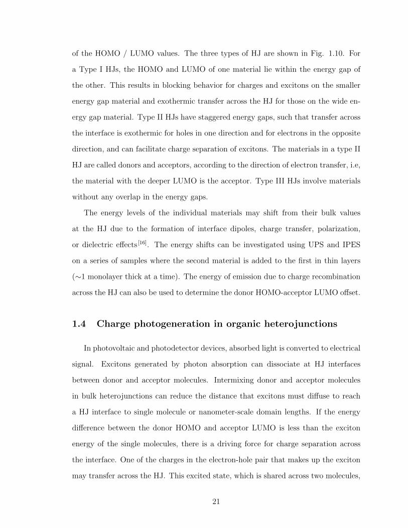
1.4 Charge photogeneration in organic heterojunctions
In photovoltaic and photodetector devices, absorbed light is converted to electrical
signal. Excitons generated by photon absorption can dissociate at HJ interfaces
between donor and acceptor molecules. Intermixing donor and acceptor molecules
in bulk heterojunctions can reduce the distance that excitons must diffuse to reach
a HJ interface to single molecule or nanometer-scale domain lengths. If the energy
difference between the donor HOMO and acceptor LUMO is less than the exciton
energy of the single molecules, there is a driving force for charge separation across
the interface. One of the charges in the electron-hole pair that makes up the exciton
may transfer across the HJ. This excited state, which is shared across two molecules,
21
Figure 1.11: Charge generation steps. 1) An incident photon is absorbed eitherin the donor (D) or acceptor (A), resulting in an exciton. 2) The excitondiffuses to a HJ interface. 3) The excition transfers to a charge-transferstate, with the electron on the acceptor. 4) The charge transfer statedissociates into free charges, which can be collected at electrodes.
is called a charge transfer state. When the charge transfer state dissociates, free
charge is generated that can then be extracted from the device at the electrodes. The
steps of the charge generation process are shown in 1.11.
The efficiency of charge photogeneration, ηCG, is simply the product of the con-
stituent step efficiencies:
ηCG = ηA × ηED × ηCT × ηCC ,
where ηA is the light absorption efficiency, ηED is the exciton diffusion efficiency, ηCT
is the charge transfer efficiency, and ηCC is the charge collection efficiency. Light
absorption is affected by light incoupling, the optical field in the thin-film structure,
layer thickness, parasitic absorption outside the HJ, and the overlap between the
absorption spectrum of the HJ and illumination source [17]. The diffusion efficiency
depends critically on the exciton diffusion length and the average distance of absorp-
tion sites from a HJ interface. Using a bulk (i.e, mixed) HJ allows the use of thicker
layers without decreasing ηED. Charge transfer efficiency is influenced by the energy
offset at the HJ and wavefunction overlap. Recent work has focused on minimizing the
22
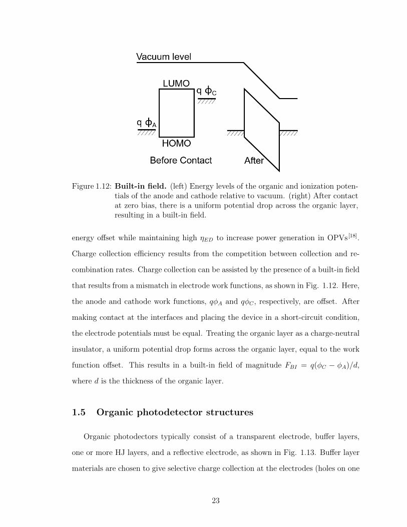
Figure 1.12: Built-in field. (left) Energy levels of the organic and ionization poten-tials of the anode and cathode relative to vacuum. (right) After contactat zero bias, there is a uniform potential drop across the organic layer,resulting in a built-in field.
energy offset while maintaining high ηED to increase power generation in OPVs [18].
Charge collection efficiency results from the competition between collection and re-
combination rates. Charge collection can be assisted by the presence of a built-in field
that results from a mismatch in electrode work functions, as shown in Fig. 1.12. Here,
the anode and cathode work functions, qφA and qφC , respectively, are offset. After
making contact at the interfaces and placing the device in a short-circuit condition,
the electrode potentials must be equal. Treating the organic layer as a charge-neutral
insulator, a uniform potential drop forms across the organic layer, equal to the work
function offset. This results in a built-in field of magnitude FBI = q(φC − φA)/d,
where d is the thickness of the organic layer.
1.5 Organic photodetector structures
Organic photodectors typically consist of a transparent electrode, buffer layers,
one or more HJ layers, and a reflective electrode, as shown in Fig. 1.13. Buffer layer
materials are chosen to give selective charge collection at the electrodes (holes on one
23

Figure 1.13: Organic photodetector structure. The heterojunction region is sep-arated from the elctrodes by buffer layers. One of the electrodes istransparent, the other reflective. A substrate-side illumination device isshown, but the device layer structure could also be inverted.
side, electrons on the other) as well as to prevent exciton quenching at the electrode
interfaces. The HJ region may comprise a planar junction between neat donor and
acceptor layers, a bulk HJ, or some combination of the two.
1.6 Photodetector current-voltage characteristics
Organic photodetector current-voltage characteristics are qualitatively similar to
inorganic PV and photodiodes. An example following the ideal diode equation, I =
IS(exp qV/kT−1)−IPh, is plotted in Fig. 1.14. Here, IS is the reverse bias saturation
current, q is the electron charge, kT is the thermal energy, and IPh is the photocurrent.
The open circuit voltage, VOC , and short circuit current, JSC , are also shown. The
red shaded region has an area of VOC × JSC . The blue shaded area intersects the
current-voltage characteristic under illumination at the maximum power point. The
ratio of the blue to red regions is defined as the fill factor (FF ). For OPVs, the power
conversion efficiency can be calculated simply as (JSC × VOC × FF )/Pincident, where
Pincident is the incident power. The ideal diode equation for organic heterojunctions
has been shown to take the same functional form as inorganic diodes, albeit with
24

Figure 1.14: Organic photodetector current voltage characteristic.
different physical underpinnings [19,20].
25
CHAPTER II
Determining polaron and exciton distributions in
organic light emitting devices
An important part of the success of PHOLEDs in the display industry has been
achieving near unity IQE through control of charge balance and exciton confine-
ment [21–25]. These are still challenging issues for long lived blue PHOLEDs due to
the energy levels required of blocking materials to confine energy to the already large
gap blue host and guest layers [21–24]. As discussed in Ch. 1, the efficiency of OLED
devices is directly proportional to ηCB and ηEC . However, it is difficult to determine
these factors in a device. A device which maximizes its theoretical EQE may be
assumed to have near unity ηCB and ηEC , but even in these cases the role of exciton
and charge confinement - and the potential loss thereof - in the roll-off of efficiency at
high brightness is uncertain. In some cases unintended emission due to fluorescence
of the transport or blocking layers indicates poor charge confinement, but the absence
of unintended emission does not guarantee that ηCB ≈ ηEC ≈ 1. In this chapter a
method for directly measuring ηCB and ηEC is introduced. The method involves dop-
ing thin sensitizing layers into the EML and its surrounding layers, and monitoring
the sensitizer emission. In addition, a model is derived that links material properties
to the blocking performance and the charge carrier and exciton distributions. The
26

technique provides a powerful tool for understanding the performance and carrier
distribution of a given device structure versus current density. The main conclusions
of this chapter were published in Advanced Optical Materials [26].
2.1 Theory of charge and exciton distributions in a PHOLED
It is important to understand charge transport and the resulting exciton density
distribution to determine an appropriate blocking layer material. Injected charges
have three possible eventualities: first, recombination in the EML; second, recombi-
nation outside of the EML; or third, they traverse the full thickness of device and
are collected at the opposing electrode. We can describe carrier transport using drift-
diffusion and thermionic emission over energy barriers [25,27,28] (for example at blocking
layer interfaces), using the equations:
Jn(x, t) = qµn(x, t)F (x, t)− kTµn(x, t)δ
δxn(x, t), (2.1)
d
dxF (x, t) =
q
ε[p(x, t)− n(x, t)] = − d2
dx2V (x, t), (2.2)
µn(x, t) = µ0n(x)exp
√F (x, t)
F0
×exp(−φp−∆φ(t)
kT) φn > ∆φ
1 φn < ∆φ
(2.3)
The hole current density, Jp(x, t), is found using an equation analogous to Eq. 2.1.
Here, F (x, t) is the electric field at position x and time t, q is the elementary charge, k
is Boltzmann’s constant, T is the temperature, and ε is the dielectric constant of the
material. Also, Jn(x, t) is the electron current density, µn(x, t) is the electron mobility,
n(x, t) is the electron density, p(x, t) is the hole density, F0 is a reference electric field,
φ is the frontier orbital energy difference across an interface, and ∆φ(t) = F (t)d is
27

the potential difference across the interface of width d. The boundary conditions are
V (0) = Va−Vbi and V (L) = 0, where Va is the applied voltage, and Vbi is the built-in
voltage. Here, x = 0 corresponds to the position at the anode side of the EML,
and x = L at the cathode. The Einstein relation is used to relate the mobility and
diffusion constants. The mobility has a Poole-Frenkel type field dependence common
to organics [29]. Charge balance is calculated from the solution to these equations,
defined quantitatively as:
ηCB =J injp − J leakp + J injn − J leakn
J injp + J injn
(2.4)
where subscripts n and p denote the polarity of the current and superscripts denote
if the current is injected into or leaking out of the EML.
Triplet excitons that are formed in the EML either relax there or diffuse into
adjacent layers. Assuming Langevin recombination [28,30], the exciton formation rate
is γ(x, t)n(x, t)p(x, t), where γ = q(µn + µp)/ε is the Langevin rate constant. We
approximate the diffusion of triplet excitons into the adjacent layers by assuming the
the diffusivity D = DN at the boundary if the triplet energy of the adjacent layer is
less than kT above the triplet energy in the EML and D = 0 otherwise. Thus, rate
equations for the polaron and exciton densities are
d
dtn(x, t) = −γ(x, t)n(x, t)p(x, t)− d
dxJn(x, t), (2.5)
d
dtp(x, t) = −γ(x, t)n(x, t)p(x, t)− d
dxJp(x, t), (2.6)
d
dtN(x, t) = γ(x, t)n(x, t)p(x, t)− d
dx
[DN(x)
d
dxN(x, t)
]. (2.7)
The spatial dependence of the mobility arises from the field dependence of the
mobility, the interface behavior mentioned above, and most importantly the spatial
dependence of the doping concentration in the EML. For triplet diffusion by the
28
Dexter transfer mechanism, the diffusivity varies with the transfer distance between
dopant sites, a, as DN ∝ a2exp(−2a
L
), where L = 1.6 nm is the exciton Bohr radius
for typical Ir based phosphors [31]. The spacing between dopant molecules is related
to the doping concentration by a = (CNM)−1/3 where C is the doping concentration
and NM ≈ 1021 is the molecular density of the film. Equations 2.1-2.3 and 2.5-2.7
are solved using a finite difference method, with initial conditions n(x, 0) = p(x, 0) =
N(x, 0) = 0. The solution is continued until the system reaches steady state.
2.2 Method of sensitizers
Exciton formation regions have previously been mapped inside a device EML
using luminescent [32,33], or quenching [25] sensitizers. The idea is to fabricate a series
of devices, each having a thin sensitizing layer embedded at a different position within
the device. The spectral intensity of the sensitizer is measured as a function of position
to determine the local density of excitons at the location of the sensor. In this work,
this concept is expanded by placing sensitizers outside the EML to monitor for leaked
excitons or charge recombination in the transport and blocking layers. We employ
ultrathin (≤2 nm) sensor layers comprising a phosphor with lower emission energy
than that of the dopant in the EML. This increases the signal due to energy transfer to
the sensitizer as well as allows sensor emission to be wavelength resolved from dopant
emission. The sensor should have a short dopant-sensor energy transfer distance, as
this limits the spatial resolution of the sensing measurement. It is also desirable to
avoid charge trapping on the sensor molecules to prevent incorporation of the sensing
layers affecting charge transport in the device [25,32]. The sensing layers trap triplet
excitons, giving red-shifted emission with intensity that is proportional to the local
density of excitons. The flux of excitons into the sensor layer at position x can be
calculated from the polaron and exciton densities as:
29
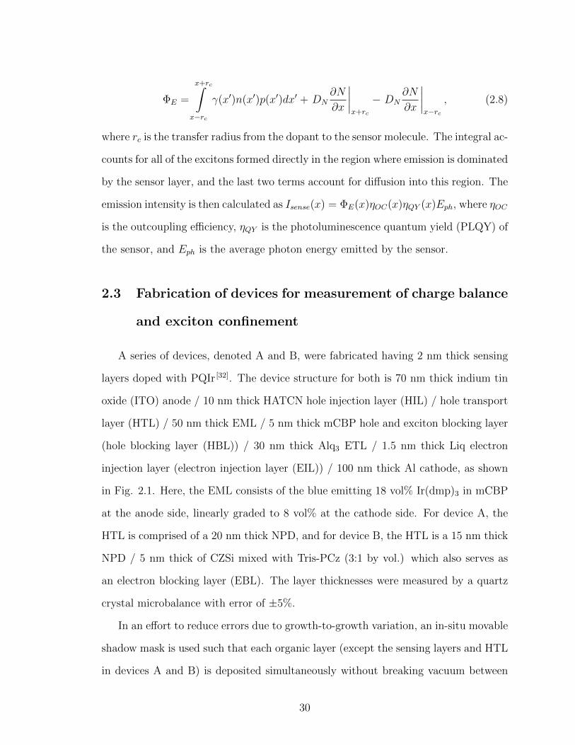
ΦE =
x+rc∫x−rc
γ(x′)n(x′)p(x′)dx′ + DN∂N
∂x
∣∣∣∣x+rc
− DN∂N
∂x
∣∣∣∣x−rc
, (2.8)
where rc is the transfer radius from the dopant to the sensor molecule. The integral ac-
counts for all of the excitons formed directly in the region where emission is dominated
by the sensor layer, and the last two terms account for diffusion into this region. The
emission intensity is then calculated as Isense(x) = ΦE(x)ηOC(x)ηQY (x)Eph, where ηOC
is the outcoupling efficiency, ηQY is the photoluminescence quantum yield (PLQY) of
the sensor, and Eph is the average photon energy emitted by the sensor.
2.3 Fabrication of devices for measurement of charge balance
and exciton confinement
A series of devices, denoted A and B, were fabricated having 2 nm thick sensing
layers doped with PQIr [32]. The device structure for both is 70 nm thick indium tin
oxide (ITO) anode / 10 nm thick HATCN hole injection layer (HIL) / hole transport
layer (HTL) / 50 nm thick EML / 5 nm thick mCBP hole and exciton blocking layer
(hole blocking layer (HBL)) / 30 nm thick Alq3 ETL / 1.5 nm thick Liq electron
injection layer (electron injection layer (EIL)) / 100 nm thick Al cathode, as shown
in Fig. 2.1. Here, the EML consists of the blue emitting 18 vol% Ir(dmp)3 in mCBP
at the anode side, linearly graded to 8 vol% at the cathode side. For device A, the
HTL is comprised of a 20 nm thick NPD, and for device B, the HTL is a 15 nm thick
NPD / 5 nm thick of CZSi mixed with Tris-PCz (3:1 by vol.) which also serves as
an electron blocking layer (EBL). The layer thicknesses were measured by a quartz
crystal microbalance with error of ±5%.
In an effort to reduce errors due to growth-to-growth variation, an in-situ movable
shadow mask is used such that each organic layer (except the sensing layers and HTL
in devices A and B) is deposited simultaneously without breaking vacuum between
30

Figure 2.1: Structure and energy diagram of PHOLEDs for confinementsensing. Energy level diagram for the materials used in devices A andB. The HOMO and LUMO energies are labeled in eV. The energies fordopants Ir(dmp)3 and PQIr are represented as dashed lines in mCBP andNPD, respectively. The 3:1 CZSi:Tris-PCz mixed layer used in device Bare indicated. For device A, x = −20 to 0 nm is replaced by neat NPD.The scale bar shows the sensing layer positions. The LUMO energies ofmCBP, Tris-PCz, and CZSi are from reduction potential measurementswith error of ±0.3 eV [34] and the remaining energies are from the liter-ature [32,34–36]. The chemical structural formulae of electron and excitonblocking materials Tris-PCz and CZSi are also shown.
31
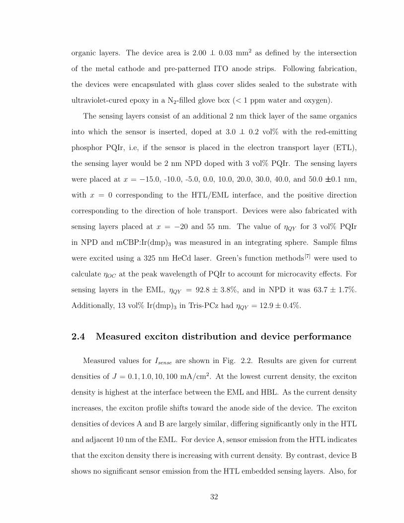
organic layers. The device area is 2.00 ± 0.03 mm2 as defined by the intersection
of the metal cathode and pre-patterned ITO anode strips. Following fabrication,
the devices were encapsulated with glass cover slides sealed to the substrate with
ultraviolet-cured epoxy in a N2-filled glove box (< 1 ppm water and oxygen).
The sensing layers consist of an additional 2 nm thick layer of the same organics
into which the sensor is inserted, doped at 3.0 ± 0.2 vol% with the red-emitting
phosphor PQIr, i.e, if the sensor is placed in the electron transport layer (ETL),
the sensing layer would be 2 nm NPD doped with 3 vol% PQIr. The sensing layers
were placed at x = −15.0, -10.0, -5.0, 0.0, 10.0, 20.0, 30.0, 40.0, and 50.0 ±0.1 nm,
with x = 0 corresponding to the HTL/EML interface, and the positive direction
corresponding to the direction of hole transport. Devices were also fabricated with
sensing layers placed at x = −20 and 55 nm. The value of ηQY for 3 vol% PQIr
in NPD and mCBP:Ir(dmp)3 was measured in an integrating sphere. Sample films
were excited using a 325 nm HeCd laser. Green’s function methods [7] were used to
calculate ηOC at the peak wavelength of PQIr to account for microcavity effects. For
sensing layers in the EML, ηQY = 92.8 ± 3.8%, and in NPD it was 63.7 ± 1.7%.
Additionally, 13 vol% Ir(dmp)3 in Tris-PCz had ηQY = 12.9± 0.4%.
2.4 Measured exciton distribution and device performance
Measured values for Isense are shown in Fig. 2.2. Results are given for current
densities of J = 0.1, 1.0, 10, 100 mA/cm2. At the lowest current density, the exciton
density is highest at the interface between the EML and HBL. As the current density
increases, the exciton profile shifts toward the anode side of the device. The exciton
densities of devices A and B are largely similar, differing significantly only in the HTL
and adjacent 10 nm of the EML. For device A, sensor emission from the HTL indicates
that the exciton density there is increasing with current density. By contrast, device B
shows no significant sensor emission from the HTL embedded sensing layers. Also, for
32

Figure 2.2: Measured and calculated values for exciton distribution. DeviceA is shown on the left and device B on the right for several currentdensities, J . All curves are normalized for comparison with the measuredprofiles. As before, the position x = 0 nm corresponds to the anode sideof the emission layer. For device A, x = −20 to 0 nm is the HTL, whilefor device B, x = −5 to 0 nm is replaced by an electron blocking layer.Error bars along the ordinate are the deviation of Isense measured fordevices from two different growths as well as error in deconvoluting PQIrand Ir(dmp)3 emission spectra. Error bars along the abscissa representuncertainty in the measured layer thicknesses.
J > 10 mA/cm2, the exciton density peaks at the EBL/EML interface. Additionally,
significant sensor emission was not observed from the HTL of device B even after the
device was degraded 50% of its initial luminance after continuous operation. This
indicates that the EBL used in device B does not degrade in a manner that allows
excitons to leak out of the EML under normal operation.
Sensing layers should not perturb charge transport and exciton density to provide
a faithful picture of charge transport in the device being studied. One indicator of
this is the deviation in the current-voltage characteristics after incorporating sensing
33
layers. In this study, the deviation in the voltage for sensing layer devices is < 10% of
the mean voltage at J = 10 mA/cm2. Additionally, the deviations are not correlated
with the sensing layer position in the device, which indicates that the incorporation
of sensing layers has not dramatically altered the charge transport properties of the
device. Additionally, we note that no sensor emission was observed from layers placed
adjacent to the HATCN HIL, which is expected because the deep energy levels of
HATCN quench excitons [32]. However, the reported diffusion length for triplets in
NPD is 87 nm [37], much greater than the thickness of the HTL, and we expect that
excitons which leak into the NPD diffuse to the HATCN interface with high efficiency,
where they are quenched.
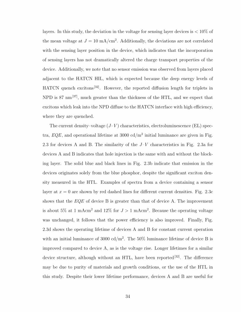
The current density–voltage (J–V ) characteristics, electroluminescence (EL) spec-
tra, EQE , and operational lifetime at 3000 cd/m2 initial luminance are given in Fig.
2.3 for devices A and B. The similarity of the J–V characteristics in Fig. 2.3a for
devices A and B indicates that hole injection is the same with and without the block-
ing layer. The solid blue and black lines in Fig. 2.3b indicate that emission in the
devices originates solely from the blue phosphor, despite the significant exciton den-
sity measured in the HTL. Examples of spectra from a device containing a sensor
layer at x = 0 are shown by red dashed lines for different current densities. Fig. 2.3c
shows that the EQE of device B is greater than that of device A. The improvement
is about 5% at 1 mAcm2 and 12% for J > 1 mAcm2. Because the operating voltage
was unchanged, it follows that the power efficiency is also improved. Finally, Fig.
2.3d shows the operating lifetime of devices A and B for constant current operation
with an initial luminance of 3000 cd/m2. The 50% luminance lifetime of device B is
improved compared to device A, as is the voltage rise. Longer lifetimes for a similar
device structure, although without an HTL, have been reported [32]. The difference
may be due to purity of materials and growth conditions, or the use of the HTL in
this study. Despite their lower lifetime performance, devices A and B are useful for
34
Figure 2.3: Performance of PHOLEDs for confinement sensing. (a) Measuredand simulated J–V characteristics of devices A and B. (b) The electrolu-minescence spectra at J = 100 mA/cm2 for both devices and example datafrom a device with embedded sensing layer at x = 0 nm (dotted lines)for J = 0.1, 1.0, 10, and 100 mA/cm2. (c) Measured external quantumefficiencies for devices A and B. Simulated efficiency of device A is alsoshown. Error bars represent the standard deviation for > 5 devices. (d)Luminance and voltage characteristics as functions of device operatingtime at constant current, with an initial luminance of 3000 cd/m2.
studying the charge balance and exciton confinement, as well as the relative lifetime
performance with and without the modifed EBL.
2.5 Modeling and discussion of results
We simulate the charge and exciton transport dynamics using the equations in
Section 2.1. Charge injection is treated identically for both devices because the J–V
characteristics are the same. The charge mobilities in the transport layers are 2-4
orders of magnitude greater than in the EML [38,39]. Because of this and to simplify
the calculation, we neglect the voltage drop over the transport layers. We determine
the parameters used for modeling current transport in the EML by fitting the electron
35
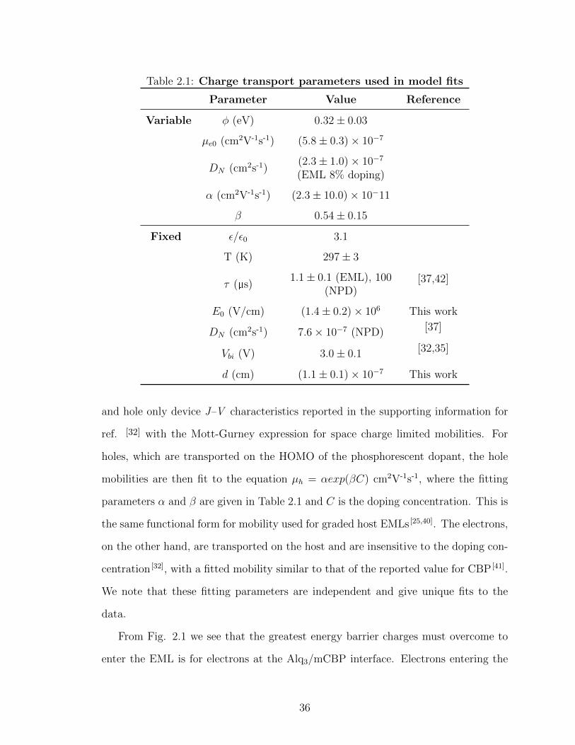
Table 2.1: Charge transport parameters used in model fits
Parameter Value Reference
Variable φ (eV) 0.32± 0.03
µe0 (cm2V-1s-1) (5.8± 0.3)× 10−7
DN (cm2s-1)(2.3± 1.0)× 10−7
(EML 8% doping)
α (cm2V-1s-1) (2.3± 10.0)× 10−11
β 0.54± 0.15
Fixed ε/ε0 3.1
T (K) 297± 3
τ (µs)1.1± 0.1 (EML), 100
(NPD)[37,42]
E0 (V/cm) (1.4± 0.2)× 106 This work
DN (cm2s-1) 7.6× 10⁻⁷ (NPD) [37]
Vbi (V) 3.0± 0.1 [32,35]
d (cm) (1.1± 0.1)× 10−7 This work
and hole only device J–V characteristics reported in the supporting information for
ref. [32] with the Mott-Gurney expression for space charge limited mobilities. For
holes, which are transported on the HOMO of the phosphorescent dopant, the hole
mobilities are then fit to the equation µh = αexp(βC) cm2V-1s-1, where the fitting
parameters α and β are given in Table 2.1 and C is the doping concentration. This is
the same functional form for mobility used for graded host EMLs [25,40]. The electrons,
on the other hand, are transported on the host and are insensitive to the doping con-
centration [32], with a fitted mobility similar to that of the reported value for CBP [41].
We note that these fitting parameters are independent and give unique fits to the
data.
From Fig. 2.1 we see that the greatest energy barrier charges must overcome to
enter the EML is for electrons at the Alq3/mCBP interface. Electrons entering the
36

mCBP HBL from Alq3 must overcome the energy offset between the LUMO energies,
φ = 0.5±0.3 eV, as calculated from the reduction potential of mCBP (-2.77 V), which
corresponds to a LUMO energy of 1.5±0.3 eV [34], and IPES measured LUMO of Alq3
is 1.96 eV. The result for the simulated current density changes significantly as the
energy offset is varied across this range, so the value of the offset is adjusted within
these bounds to achieve the best fit. The barrier width, d = 1.1 nm, approximately
corresponds to the molecular spacing. Holes injecting into the EML face no significant
energy barriers. The large HOMO offset at the interface between the EML and HBL
(∼ 1 V difference between Ir(dmp)3 and mCBP) effectively blocks holes. Finally,
ohmic contact is assumed between the electrodes and transport layers [43,44]. With
this assumption, the built-in voltage is the potential between the HOMO level of
Ir(dmp)3 and the LUMO level of Alq3.
Because NPD fluorescence between 400-450 nm [45,46] is not observed in the EL
spectra of the devices while significant sensor emission is observed from the NPD
layer of device A, we conclude that the leaking species are triplet excitons from the
EML. Thus, the improvement of device B by incorporating a blocking layer is due
to improving exciton confinement rather than charge balance. The energies of the
layers are consistent with this conclusion: NPD has a triplet energy of 2.3 eV [47], less
than that of Ir(dmp)3 (2.7 eV). This means that exciton transfer into the HTL is
exothermic for device A, whereas the NPD LUMO is high enough to provide some
barrier to electrons. The EBL of device B comprises Tris-PCz and CZSi, which
have triplet levels of 2.8 eV and 3.1 eV, respectively [36,48]. Thus, a mixture of these
materials has a sufficiently high triplet energy to block excitons from the EML, as
verified by the lack of emission from sensing layers in the HTL of device B. Thus, at
the HTL/EML interface, D = 0 for device B but D = DN for device A.
The diffusion constant of the triplets is obtained by fitting it to the ratio of red
to blue emission from the sensor layers. As shown in Eq. 2.8, the intensity of sensor
37

emission increases with the value of D. The fitted value of D yields LD =√Dτ = 5±1
nm at 8 vol% Ir(dmp)3, which is comparable to the reported value of 6.8 nm for
Ir(ppy)3 doped with the same concentration into CBP [49].
The results of the simulation are shown in Fig. 2.2. All parameter values are re-
ported in Table 2.1. The solid blue lines correspond to the calculated exciton density,
and the red points represent the emission intensity calculated using the exciton profile
and Eq. 2.8. There is good agreement between the fit and the measured results across
the full range of measured current densities. From these results, we understand that
the decrease in sensor emission intensity at x = 0 nm compared to x = 10 nm in
device A, which is not present for device B, is the result of exciton diffusion into the
HBL. The simulated J–V in Fig. 2.3 are in good agreement with experiment in the
space charge region, however the trapping that dominates the J–V characteristics at
< 5 V were not considered by the model, resulting in deviation of the fit from the
data.
The calculated polaron profiles are shown in Fig. 2.4. We find that at low bias,
holes are efficiently injected due to the lack of energy barrier. This results in hole
accumulation at the EML/HBL interface and a corresponding large density of excitons
there. Electrons are injected over the barrier formed by the LUMO offset energy,
which separates a large electron density from the holes. Thus, the field is maximum
and nearly constant across the 5 nm thick HBL. As the voltage and carrier build up
increases, the field across the HBL also increases, lowering the barrier and speeding
up electron injection into the EML exponentially. Electrons near the cathode side of
the EML have a higher mobility than holes at the same location due to the scarcity
of hole-transporting dopant sites there. Thus, with increasing bias the electrons
penetrate deeper into the EML as the electron current increases. This shifts the
recombination zone towards the HTL, and the polarity of the net space charge on the
HBL side becomes negative. This causes the voltage drop over the HBL to increase
38

Figure 2.4: Calculated polaron profiles and electron injection energy barrierreduction. (a) Simulated hole and electron densities corresponding tothe results in Fig. 2.2. Holes are blocked by HBL at x = 50 nm andelectrons are blocked at the anode side of the EML at x = 0 nm. Theelectron current at is reduced by the energy barrier at the HBL/ETL in-terface at x = 55 nm. At low voltage, holes (solid line, squares) buildup at the HBL/ETL interface, while electrons build up at the ETL/HBLinterface, with a low injected electron density in the EML. As the appliedvoltage increases, the barrier height to electron injection into the HBLdecreases and electrons penetrate deeper into the EML. (b) Electron in-jection barrier height φn −∆φ vs. voltage. As electrons are injected intothe EML, negative space charge decreases the barrier height. The slope ofthe dotted line shows the initial rate of barrier reduction for comparison.
39
more slowly with increasing voltage than it did at lower voltages. The effective barrier
height is plotted in Fig. 2.4. At low bias it decreases linearly with voltage (dotted
curve), but the decrease becomes sub-linear with increasing bias (solid curve). We
note that the asymmetric injection barriers cause holes to outnumber electrons in the
EML even when the exciton recombination zone is near the anode side of the EML.
Also, we find that an efficient blocking layer material must have energy levels that
are inaccessible by thermal excitation to charges and excitons in the EML.
Calculating the loss of EQE due to exciton leakage in device A, we find that
2.3 ± 0.1% loss is expected at J = 0.1 mA/cm2, which increases to 11.9 ± 0.1% at
100 mA/cm2. This is shown in Fig. 2.3b. The simulated efficiency is the measured
efficiency of device A plus the calculated exciton loss. The discrepancy between
the simulated efficiency and that of device B is likely due to inaccuracy in model
parameters.
The relative lack of exciton confinement in the EML of device A is not apparent
from the OLED J − V , luminance, and EL spectral characteristics and changes with
current density. In general, a device may exhibit poor charge balance only in certain
regimes, e.g. high or low current, complicating the evaluation of the blockers. In the
devices considered here, there is significant leakage of triplets into NPD which does
not appear in the PHOLED emission spectrum, and also does not occur at low current
density. The sensing layers, therefore, provide an accurate means for determining if
charge balance and exciton confinement are achieved using the blocking material of
interest. Indeed, a device such as this could achieve maximum theoretical efficiency
at low current density, and be erroneously assumed to have unity charge balance and
exciton confinement.
Intrinsic degradation in blue PHOLEDs has been attributed to bi-molecular an-
nihilation reactions, such as TPA [6,32,42,50]. The high energy of resulting hot excited
states may cause bond rupture in the organic molecules, resulting in molecular frag-
40

ments [51–53] that trap charges and quench excitons, leading to voltage rise and lu-
minance loss, respectively. Because reactions such as TPA and TTA occur more
frequently at high current density, increasing device efficiency will reduce the current
required to reach high brightness, improving reliability. Additionally, spreading the
exciton density uniformly across the EML will reduce the TPA rate at a given bright-
ness [32]. Another degradation mechanism that has been reported is due to molecular
instability of some ionic excited states [42,54]. For example, Alq3 has been reported to
have an unstable cation (i.e. the charge state when carrying holes) [54]. Both of these
mechanisms are addressed by improving ηCB and ηEC . We attribute the improved
lifetime performance of device B shown in Fig. 2.3d to the improved efficiency and
reduced exciton leakage into the HTL.
2.6 Summary
We have developed a framework for studying and measuring charge and exciton
leakage in PHOLEDs using thin luminescent sensing layers. The quantitative model
can be used to accurately describe the charge and exciton densities within the de-
vice, which is confirmed by the good agreement between the measured results using
sensing layers and the calculated values for exciton density. Inserting an appropri-
ate EBL improves exciton confinement in the EML, resulting in an increased EQE
and operational lifetime. Sensing layers are particularly useful for characterizing blue
PHOLEDs, where large carrier and exciton energies make it difficult to optimize
charge balance and exciton confinement in the EML. Further, detailed knowledge
of the exciton profile evolution with current density can lead to the engineering of
recombination zones with broad, uniform exciton distributions useful for reducing ef-
ficiency roll-off [25] and increasing PHOLED lifetime [32]. We find that suitable blockers
have LUMO and triplet energies that are inaccessible by thermal excitation from the
EML, and that their operational stability can be evaluated using sensing layers em-
41
bedded within the transport layers. Indeed, the contribution of the blocking layer to
device degradation can be evaluated by monitoring the emission from sensing layers
embedded into the blocking or transport layers. This separates the effects of blocking
layer degradation from other mechanisms, such as intrinsic degradation of dopant or
host [32,42,50]. The effects of changes in charge balance and exciton confinement on
device reliability will be discussed in greater detail in Ch. III.
42
CHAPTER III
The effect of charge balance and exciton
confinement on phosphorescent organic light
emitting device lifetime
In Ch. II, a method for determining charge balance and exciton confinement in
PHOLEDs was introduced. Some attention was given to the effect of static values
of ηCB and ηEC on the stability of devices. In this chapter, this study is expanded
to measure the effect of changes in ηCB and ηEC on the operational lifetime of the
device.
The usefulness of PHOLEDs in displays and other practical applications depends
crucially on their reliability [55,56]. However, the lifetime of blue PHOLEDs is often too
short for commercial applications, whereas green and red devices have already been
adopted for display and lighting. Thus, detailed understanding of the challenges to
be overcome for achieving highly reliable blue PHOLEDs is an important endeavor.
Research on blue device reliability has primarily focused on the intrinsic degradation
of the host guest system in the EML [6,32,50,54]. While intrinsic degradation of the
EML is well established, other mechanisms may also contribute to luminance loss.
Particularly, loss of charge balance or exciton confinement would directly affect the
43
luminance of devices. Thus, degradation of the blocking layers, increased resistance,
or changes in the layer morphology can decrease the device reliability. By monitoring
the emission of sensing layers embedded in the transport layers of a blue PHOLED,
we measure the charge balance and exciton confinement efficiency as a function of
operating time. We find that changes in exciton confinement do contribute to lumi-
nance loss, but only marginally (< 5% of total luminance loss). The main conclusions
of this chapter were published in Physical Review Applied [57].
3.1 Measuring charge balance and exciton confinement in
PHOLEDs
As in Ch. II, we employ thin red-emitting phosphorescent sensing layers embedded
at strategic locations in the device. In the present study, we employ both fluorescent
and phosphorescent red emitters in the sensing layers, which allows us to distinguish
charge and exciton leakage. If we assume that the phosphor in the sensing layer effi-
ciently collects all leaked charges and excitons, then the charge balance efficiency ηCB
and exciton confinement efficiency ηEC are related to the measured sensor emission
photon flux ΦP by:
ηCBηEC = 1− qΦP
JηOCηEUηQY. (3.1)
Here, q is the electron charge, J is the current density, ηOC is the outcoupling efficiency
of the sensor emission, ηEU = 1 is the exciton utilization efficiency of the sensor layer,
and ηQY is the quantum yield of the sensing layer emitter. Charges that recombine in
the EML either directly form triplet excitons, or form singlets which rapidly convert
to triplet excitons via intersystem crossing (ISC) [1,58]. Because triplets on fluorescent
dopants are not emissive at room temperature, fluorescent sensors only emit if singlets
are formed by charge recombination in the transport layer or due to Forster transfer
44
from the EML. Forster transfer can be prevented by spacing the sensing layer a
sufficient distance from the EML, thus the fluorescent sensor can be made sensitive
only to charge leakage (and recombination) in the transport layer. To quantify this
leakage, ηEC is set to one and ηEU is set to 0.25 in Eq. 3.1. Thus, by measuring
emission from both phosphorescent and fluorescent sensing layers in the HTL and
ETL, ηCB and ηEC can be determined individually.
3.1.1 Requirements for sensing molecules
Appropriate emissive sensing materials should have a HOMO energy that is the
same or deeper than the HTL, and a LUMO that is the same or shallower than the
ETL. These properties prevent the dopant from trapping charge and altering charge
transport in the layer. In addition, the exciton energy should be less than that of the
hosting material to allow for efficient ηET and emission. This also implies that the
sensor emission will be easily spectrally resolvable from the primary emission of the
device.
3.2 Fabrication of devices for measurement of charge balance
and exciton confinement vs. operating time
Three sensing devices: PtOEP-HTL sensing, PtOEP-ETL sensing, and DCM2-
ETL sensing, were grown by vacuum thermal evaporation (VTE) at a base pressure
< 5×10⁻⁷ torr on solvent-cleaned substrates comprising a pre-patterned, 70 nm thick
indium tin oxide (ITO, 60 ± 10 Ω/sq.) layer on glass. The substrates were exposed
to UV-ozone for 10 min immediately prior to loading into the VTE chamber. The 2
mm2 device area is defined by the intersection of the ITO anode and the 100 nm thick
Al cathode, the latter patterned by deposition through a shadow mask. The device
structure for the PtOEP-ETL sensing device is: ITO anode / 10 nm HATCN HIL /
45
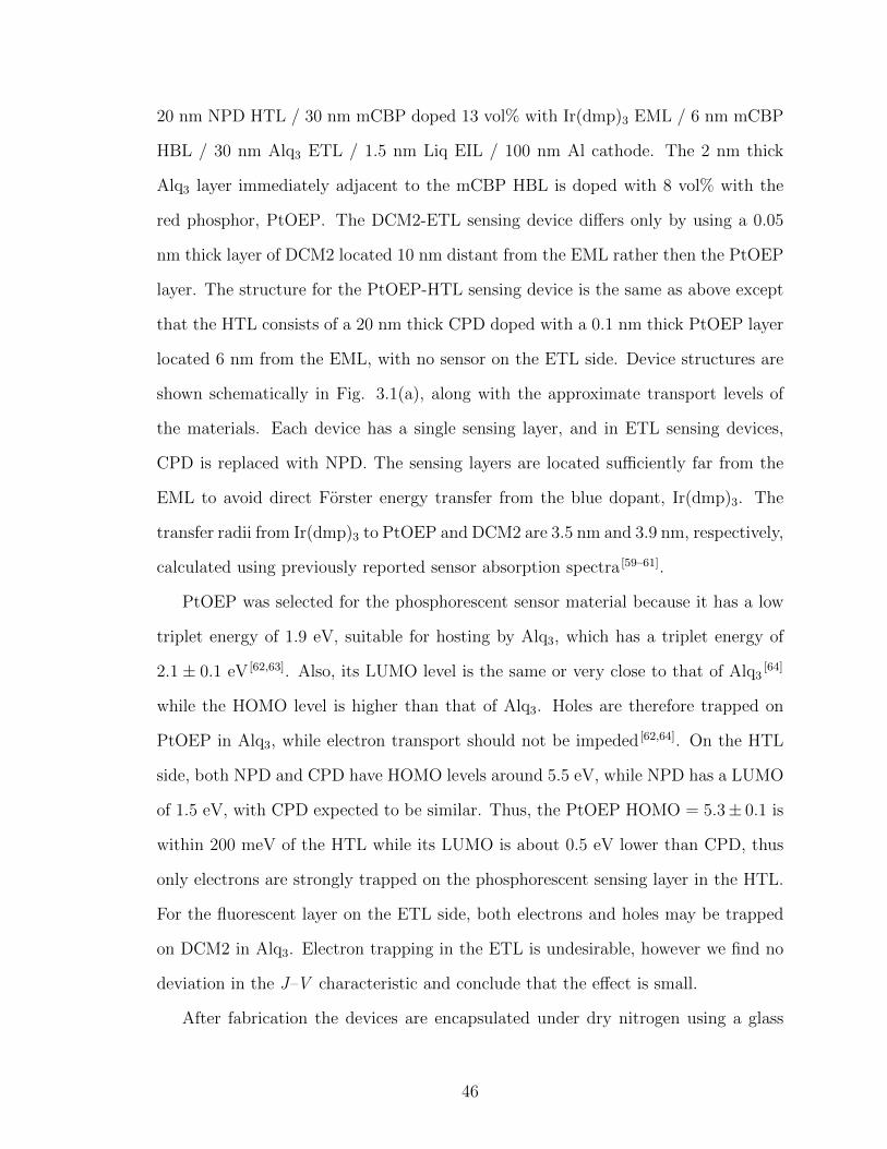
20 nm NPD HTL / 30 nm mCBP doped 13 vol% with Ir(dmp)3 EML / 6 nm mCBP
HBL / 30 nm Alq3 ETL / 1.5 nm Liq EIL / 100 nm Al cathode. The 2 nm thick
Alq3 layer immediately adjacent to the mCBP HBL is doped with 8 vol% with the
red phosphor, PtOEP. The DCM2-ETL sensing device differs only by using a 0.05
nm thick layer of DCM2 located 10 nm distant from the EML rather then the PtOEP
layer. The structure for the PtOEP-HTL sensing device is the same as above except
that the HTL consists of a 20 nm thick CPD doped with a 0.1 nm thick PtOEP layer
located 6 nm from the EML, with no sensor on the ETL side. Device structures are
shown schematically in Fig. 3.1(a), along with the approximate transport levels of
the materials. Each device has a single sensing layer, and in ETL sensing devices,
CPD is replaced with NPD. The sensing layers are located sufficiently far from the
EML to avoid direct Forster energy transfer from the blue dopant, Ir(dmp)3. The
transfer radii from Ir(dmp)3 to PtOEP and DCM2 are 3.5 nm and 3.9 nm, respectively,
calculated using previously reported sensor absorption spectra [59–61].
PtOEP was selected for the phosphorescent sensor material because it has a low
triplet energy of 1.9 eV, suitable for hosting by Alq3, which has a triplet energy of
2.1± 0.1 eV [62,63]. Also, its LUMO level is the same or very close to that of Alq3[64]
while the HOMO level is higher than that of Alq3. Holes are therefore trapped on
PtOEP in Alq3, while electron transport should not be impeded [62,64]. On the HTL
side, both NPD and CPD have HOMO levels around 5.5 eV, while NPD has a LUMO
of 1.5 eV, with CPD expected to be similar. Thus, the PtOEP HOMO = 5.3± 0.1 is
within 200 meV of the HTL while its LUMO is about 0.5 eV lower than CPD, thus
only electrons are strongly trapped on the phosphorescent sensing layer in the HTL.
For the fluorescent layer on the ETL side, both electrons and holes may be trapped
on DCM2 in Alq3. Electron trapping in the ETL is undesirable, however we find no
deviation in the J–V characteristic and conclude that the effect is small.
After fabrication the devices are encapsulated under dry nitrogen using a glass
46

Figure 3.1: Structure and performance of PHOLEDs for confinement sens-ing vs operating time. (a) Schematic representation of devices. Theenergy levels of the organic layers, including the dopants and sensors aredenoted inside the boxes, measured in eV from the vacuum level. Defi-nitions of the acronyms used for each material are defined in text. Notethat for the ETL-side sensing devices, the HTL is NPD rather than CPD.Each device contains a single sensing layer. (b) Current-density vs. volt-age characteristics of the as-grown devices. Reference devices omit sensinglayers but are otherwise unchanged. (c) Luminance (L) normalized to itsinitial value (L0), and voltage rise (∆V ) vs. operating time at 30 mA/cm2
for PtOEP-HTL and -ETL side sensing devices.
47

cover slide attached by UV curable epoxy at the edges. The current-voltage-luminance
characteristics of the device were measured immediately following fabrication. Then,
two of each device structure were operated at 30 mA/cm2, and the EL spectra were
measured at 1 and 10 mA/cm2 every time the luminance dropped by about 5% (i.e.
at T100, T95, T90, etc.).
3.3 Experimental results
To measure the quantum yield of the various sensor/host combinations, films with
the following structures were fabricated on quartz substrates for measurement of ηQY :
25 nm thick Alq3 doped with 8 vol% PtOEP, 5 nm CPD / 0.1 nm PtOEP / 5 nm CPD
/ 0.1 nm PtOEP / 5 nm CPD, and 5 nm Alq3 / 0.05 nm DCM2 / 5 nm Alq3 / 0.05 nm
DCM2 / 5 nm Alq3. The films were measured in an integrating sphere under nitrogen
flow using a 325 nm HeCd laser as an excitation source. The quantum yield of the
PtOEP:Alq3 film was measured to be 14.9 ± 1.6%; PtOEP:CPD film, 28.5 ± 1.9%;
and DCM2:Alq3 film, 50 ± 9%. Green’s function methods were used to calculate
ηOC using optical constants for the various organic films obtained by ellipsometry,
yielding ηOCηQY = 2.3 ± 0.2% for the PtOEP-ETL sensing layer; 5.1 ± 0.2% for the
PtOEP-HTL sensing layer, and 7.5± 1.4% for the DCM2-ETL sensing layer.
The J–V characteristics of the PtOEP-ETL and PtOEP-HTL sensing devices,
together with those for reference devices that do not have sensing layers are shown
in Fig. 3.1b. The characteristics are similar for all devices, with slight variations
due to different HTL materials and growth-to-growth variations. The DCM2-ETL
sensing device, which is not plotted, also shows a similar characteristic to its reference
device. The peak EQE of the devices was 8.8%. Luminance loss and voltage rise vs
operating time at J = 30 mA/cm2 are plotted in Fig. 3.1c for the PtOEP-HTL and
-ETL sensing devices. All devices show the same luminance loss and voltage rise,
independent of the sensing layers.
48
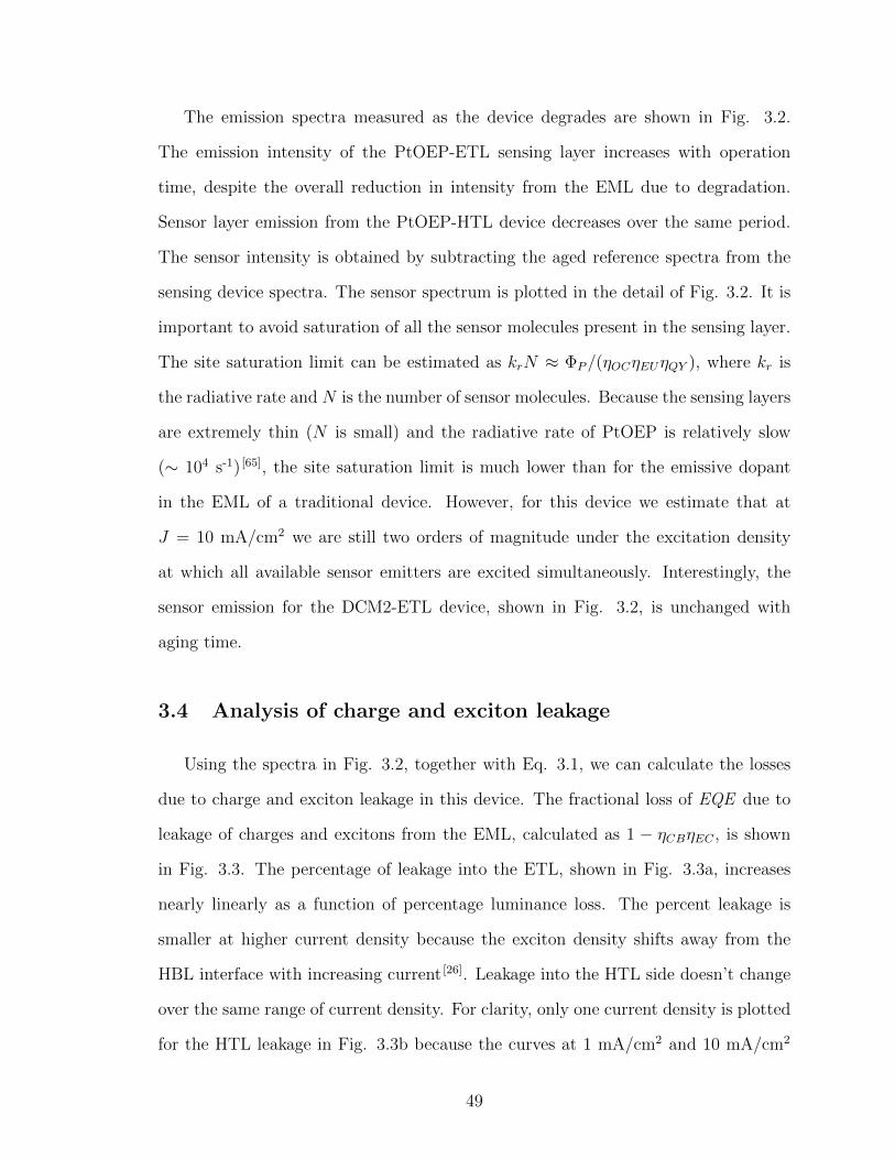
The emission spectra measured as the device degrades are shown in Fig. 3.2.
The emission intensity of the PtOEP-ETL sensing layer increases with operation
time, despite the overall reduction in intensity from the EML due to degradation.
Sensor layer emission from the PtOEP-HTL device decreases over the same period.
The sensor intensity is obtained by subtracting the aged reference spectra from the
sensing device spectra. The sensor spectrum is plotted in the detail of Fig. 3.2. It is
important to avoid saturation of all the sensor molecules present in the sensing layer.
The site saturation limit can be estimated as krN ≈ ΦP/(ηOCηEUηQY ), where kr is
the radiative rate and N is the number of sensor molecules. Because the sensing layers
are extremely thin (N is small) and the radiative rate of PtOEP is relatively slow
(∼ 104 s-1) [65], the site saturation limit is much lower than for the emissive dopant
in the EML of a traditional device. However, for this device we estimate that at
J = 10 mA/cm2 we are still two orders of magnitude under the excitation density
at which all available sensor emitters are excited simultaneously. Interestingly, the
sensor emission for the DCM2-ETL device, shown in Fig. 3.2, is unchanged with
aging time.
3.4 Analysis of charge and exciton leakage
Using the spectra in Fig. 3.2, together with Eq. 3.1, we can calculate the losses
due to charge and exciton leakage in this device. The fractional loss of EQE due to
leakage of charges and excitons from the EML, calculated as 1 − ηCBηEC , is shown
in Fig. 3.3. The percentage of leakage into the ETL, shown in Fig. 3.3a, increases
nearly linearly as a function of percentage luminance loss. The percent leakage is
smaller at higher current density because the exciton density shifts away from the
HBL interface with increasing current [26]. Leakage into the HTL side doesn’t change
over the same range of current density. For clarity, only one current density is plotted
for the HTL leakage in Fig. 3.3b because the curves at 1 mA/cm2 and 10 mA/cm2
49
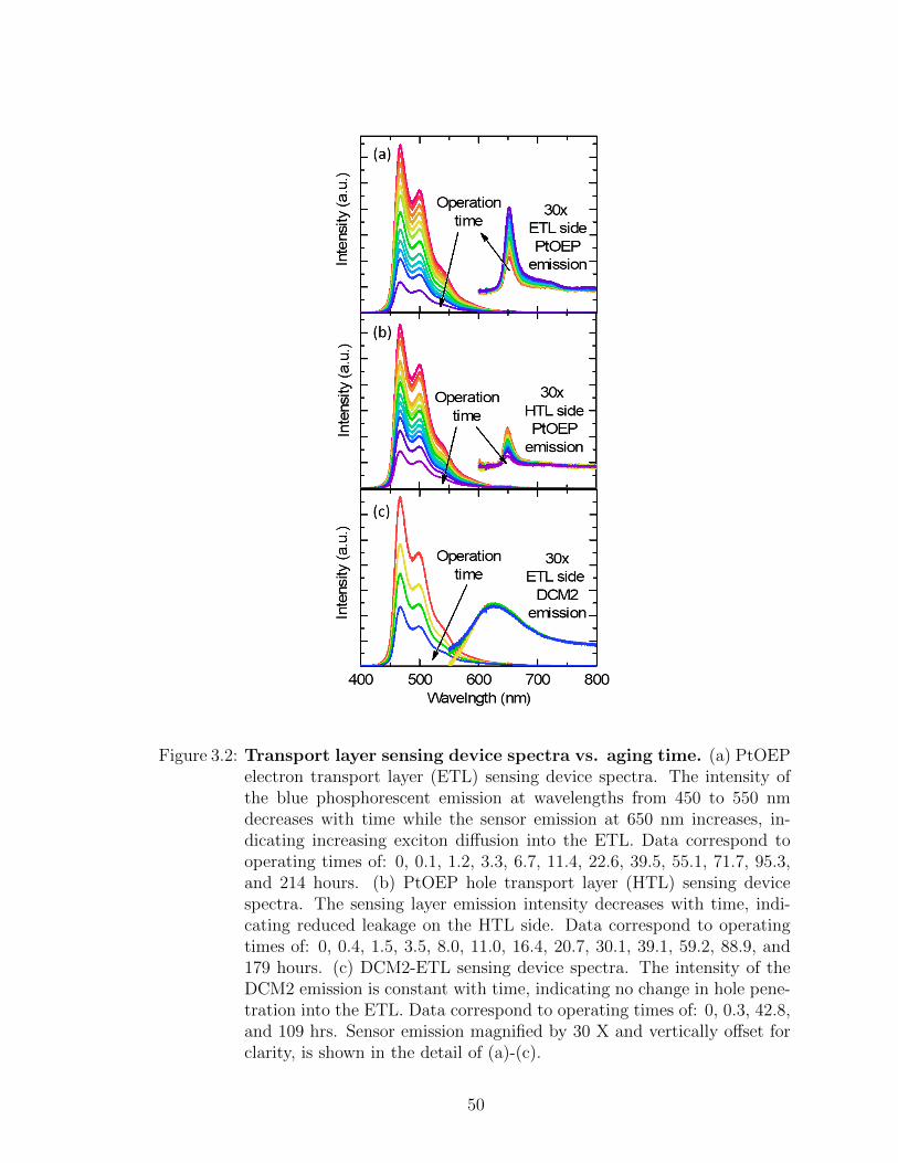
Figure 3.2: Transport layer sensing device spectra vs. aging time. (a) PtOEPelectron transport layer (ETL) sensing device spectra. The intensity ofthe blue phosphorescent emission at wavelengths from 450 to 550 nmdecreases with time while the sensor emission at 650 nm increases, in-dicating increasing exciton diffusion into the ETL. Data correspond tooperating times of: 0, 0.1, 1.2, 3.3, 6.7, 11.4, 22.6, 39.5, 55.1, 71.7, 95.3,and 214 hours. (b) PtOEP hole transport layer (HTL) sensing devicespectra. The sensing layer emission intensity decreases with time, indi-cating reduced leakage on the HTL side. Data correspond to operatingtimes of: 0, 0.4, 1.5, 3.5, 8.0, 11.0, 16.4, 20.7, 30.1, 39.1, 59.2, 88.9, and179 hours. (c) DCM2-ETL sensing device spectra. The intensity of theDCM2 emission is constant with time, indicating no change in hole pene-tration into the ETL. Data correspond to operating times of: 0, 0.3, 42.8,and 109 hrs. Sensor emission magnified by 30 X and vertically offset forclarity, is shown in the detail of (a)-(c).
50
Figure 3.3: Percentage of charges and excitons lost to transport layers. Per-cent leakage, 100%(1−ηCBηEC), on (a) the ETL and (b) the HTL side ofthe blue phosphorescent organic light emitting device at J = 1 mA/cm2
and 10 mA/cm2, vs. the percent luminance loss, L/L0. The dashed lineis a fit to the HTL side leakage. The HTL leakage decreases with timeand is the same at both J=1 and 10 mA/cm2 (not shown). Error barsrepresent the differences between two samples of each device type.
are overlapping. Error bars represent the variation between similar devices.
Because DCM2-ETL sensor emission is constant, we conclude that ηCB is not
changing with device degradation. This is expected, as Alq3 emission (as well as
NPD emission) are absent from the aged spectra of all the devices. This implies that
the increased emission from the PtOEP-ETL sensing layer is due to increasing triplet
exciton leakage into the ETL.
Triplet exciton blocking at the EML/mCBP interface relies on the high triplet
level of mCBP (2.95 eV [36]) relative to that of the phosphor Ir(dmp)3 (2.7±0.1 eV).
51
One possible explanation for increasing exciton leakage into the EML is the generation
of low triplet energy degradation products in the HBL. Several such fragments have
been identified in studies of mCBP degradation routes in OLEDs [66,67]. An alternative
explanation is morphological changes in the EML, which affects reliability of OLEDs
and could play a role here [68]. For example, crystalite formation in the HBL could
cause intermixing of the adjacent layers or local uneven film thickness and incomplete
coverage.
HTL leakage in analogous devices has been attributed to exciton diffusion [26,69].
This is possible because of the low triplet energy of NPD compared to the EML.
We note again that HTL material fluorescence is not observed, indicating electron
recombination is not occuring in the HTL.
To understand the decrease in sensor emission from the PtOEP-HTL device, we
need to separate two possible effects: First, as the device ages, excitons in the EML
are expected to recombine more quickly due to quenching on defect sites, and thus the
flux of excitons diffusing into the HTL should decrease. Second, changes in charge
conduction with device aging could shift the recombination zone further from the
HTL. We investigate these effects by solving the diffusion equation together with a
TPA degradation model that considers defect generation, non-radiative recombination
on defects, and exciton quenching [6]. Specifically, we solve the set of equations:
d
dtp(t, t′) =
J
qd− γn(t, t′)p(t, t′)− ktrapQ(t′)p(t, t′) (3.2)
d
dtn(t, t′) =
J
qd− γn(t, t′)p(t, t′)− krecQ(t′)n(t, t′) (3.3)
d
dtT (x, t, t′) =
d
dx
[D(x)
d
dxT (x, t, t′)
]+ γn(t, t′)p(t, t′)
−[
1
τ0
+ kquenchQ(x, t′)
]T (x, t, t′)
(3.4)
52
d
dt′Q(x, t′) = kxn(t′)T (x, t′), (3.5)
Here the independent variables are t, the time on the timescale of generation and
transport (on the order of microseconds); t′, the time on the timescale of degradation
and defect generation (timescale of hours); and x, the position. The independent
variables n(t, t′), p(t, t′), T (x, t, t′), and Q(x, t′) are the electron, hole, free triplet, and
defect densities, respectively. Additionally, D(x) is the diffusivity, J is the current
density, q is the electron charge, d = 30 nm is the EML width, γ = 1.7 × 10⁻¹³
cm3s-1 is the Langevin recombination rate, n(t, t′) and p(t, t′) are the electron and
hole densities, respectively, ktrap = 1.4 × 10⁻¹³ cm3s-1 is the charge trapping rate
constant, Q(x, t′) is the defect density, krec = 4.8×10⁻¹⁴ cm3s-1 is the trapped charge
recombination rate constant, τ0 = 1.1 µs is the exciton lifetime in the fresh device,
kquench = 5 × 10⁻¹² cm3s-1 is the rate constant for quenching of excitons by traps,
and kx = 7 × 10⁻²⁴ cm3s-1 is the defect generation rate constant. The values of the
rate constants used here were reported previously for this host/dopant system [6]. The
free triplet density is zero at the sensing layer, corresponding to complete trapping
on the sensing molecules, and excitons are assumed to be blocked at the HBL. In the
HTL, D = 2.3× 10⁻⁷ cm2s-1 and τ = 100 µs [26]. In the EML D = 7.6× 10⁻⁷ cm2s-1,
while τ ranges from 1.1 µs in the pristine device to 0.5 µs at L/L0 = 0.16 [6], with
intermediate values obtained by linear interpolation. The exciton flux at the sensing
layer is D(x)dT (x,∞,t′)dx
, evaluated at the position of the sensing layer.
To solve this equation set, we first solve Eq. 3.3-3.4 in steady state ( ddt→ 0) for
the charge and exciton densities as functions of Q. We then solve Eq. 3.5 for the
time evolution of Q(x, t′). Finally, the diffusive flux of excitons into the HTL is taken
from the solution to Eq. 3.4. This predicts a trend for the rate of exciton leakage
vs luminence loss, which is then fit to the data in Fig. 3.3b. The good agreement
between the intrinsic degradation model and measured reduction in sensor emission
53
indicates that the measured effect is fully accounted for by the reduction in exciton
density and the exciton diffusion length due to the generation of defects as the device
ages.
The contribution of loss of charge balance and exciton confinement to luminance
loss is:
∆LCB(t′) =1− [ηCB(t′)ηEC(t′)− ηCB(0)ηEC(0)])
1− L/L0
. (3.6)
The result for ∆LCB(t′), calculated using PtOEP-HTL and PtOEP-ETL data, is
shown in Fig. 3.4. Error bars are the difference in ∆LCB(t′) calculated for similar
devices. Thus, we find that loss of exciton confinement accounts for approximately
3% of luminance loss at J = 1 mA/cm2, and 1-2% at J = 10 mA/cm2. This implies
that intrinsic degradation of the EML is responsible for ∼97% of luminance loss,
validating the assumption of dominant intrinsic degradation in previous work on the
lifetime of blue PHOLEDs [6,32,42].
3.5 Summary
In conclusion, we have developed a technique for quantifying charge and exciton
leakage into transport layers of OLEDs, which is particularly useful for evaluating
phosphorescent devices to the nonradiative nature of leaked triplet excitons. We
find that for a test blue PHOLED structure the charge balance is unchanged with
lifetime, while exciton confinement efficiency degrades so slowly as to be almost neg-
ligible compared to intrinsic degradation. These results may vary greatly based on
the device structure being evaluated, and the effect of charge balance and exciton
confinement should be evaluated on a case by case basis. However, it is likely that
significant improvement in the reliability of blue PHOLEDs will require more robust
host and dopant molecules. This may be accomplished by judicious molecular de-
54
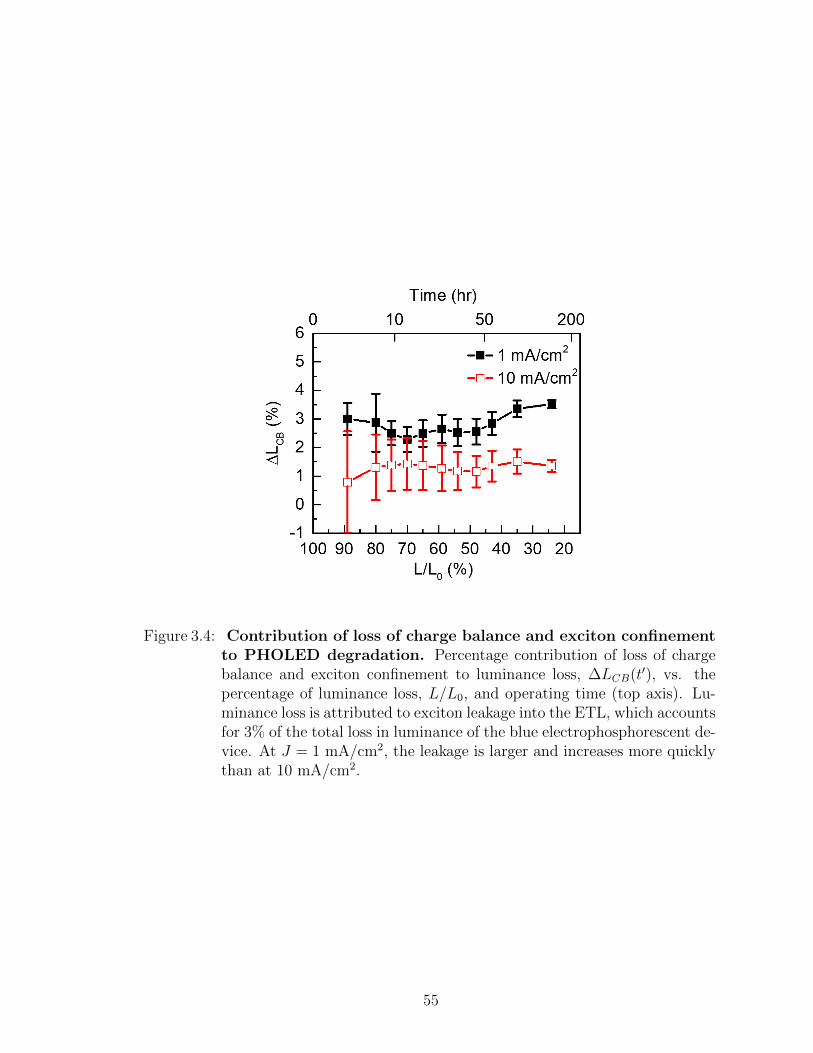
Figure 3.4: Contribution of loss of charge balance and exciton confinementto PHOLED degradation. Percentage contribution of loss of chargebalance and exciton confinement to luminance loss, ∆LCB(t′), vs. thepercentage of luminance loss, L/L0, and operating time (top axis). Lu-minance loss is attributed to exciton leakage into the ETL, which accountsfor 3% of the total loss in luminance of the blue electrophosphorescent de-vice. At J = 1 mA/cm2, the leakage is larger and increases more quicklythan at 10 mA/cm2.
55

sign to reduce coupling to the degradation pathways of the molecules or structural
strategies [25,32,70,71].
56
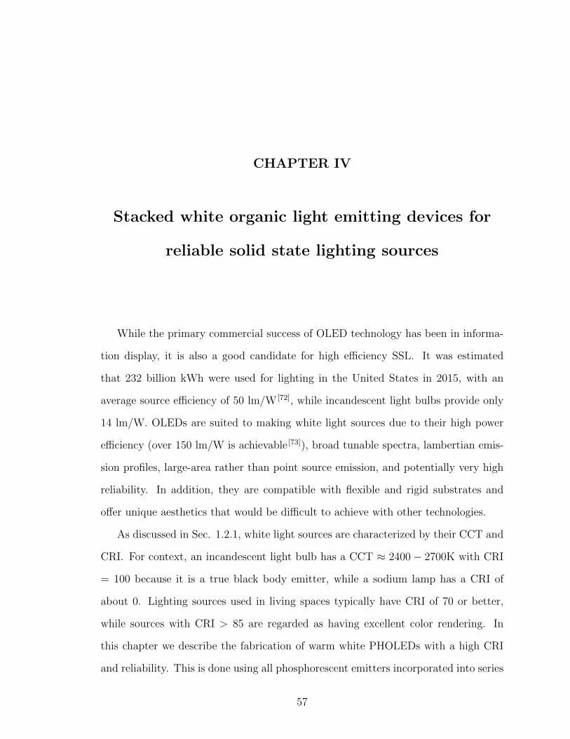
CHAPTER IV
Stacked white organic light emitting devices for
reliable solid state lighting sources
While the primary commercial success of OLED technology has been in informa-
tion display, it is also a good candidate for high efficiency SSL. It was estimated
that 232 billion kWh were used for lighting in the United States in 2015, with an
average source efficiency of 50 lm/W [72], while incandescent light bulbs provide only
14 lm/W. OLEDs are suited to making white light sources due to their high power
efficiency (over 150 lm/W is achievable [73]), broad tunable spectra, lambertian emis-
sion profiles, large-area rather than point source emission, and potentially very high
reliability. In addition, they are compatible with flexible and rigid substrates and
offer unique aesthetics that would be difficult to achieve with other technologies.
As discussed in Sec. 1.2.1, white light sources are characterized by their CCT and
CRI. For context, an incandescent light bulb has a CCT ≈ 2400− 2700K with CRI
= 100 because it is a true black body emitter, while a sodium lamp has a CRI of
about 0. Lighting sources used in living spaces typically have CRI of 70 or better,
while sources with CRI > 85 are regarded as having excellent color rendering. In
this chapter we describe the fabrication of warm white PHOLEDs with a high CRI
and reliability. This is done using all phosphorescent emitters incorporated into series
57

stacked devices to achieve high operational stability. The main conclusions of this
chapter were published in ACS Photonics [74].
4.1 Determining the spectrum for a white light source
As discussed in Ch. I, the human eye is only sensitive to light in the wavelength
range 400-700 nm. Therefore, to maximize power efficiency while maintaining good
color rendering, it is desirable to achieve a spectrum similar to that of a black body
source of the same CCT in the visible, but with no intensity outside visible wave-
lengths. Typical Ir based phosphors, such as FIrpic and Ir(ppy)3 have full width at
half maximum (FWHM) of about 60-100 nm. Thus, good coverage of the full visi-
ble spectrum can be achieved with three emitters, typically a blue, green, and red.
Two-emitter [75–77] and even single-emitter [78] schemes are also possible, however the
CRI suffers as a result of poor spectral adaptability. Here, we choose Ir(dmp)3 as the
blue emitter, Ir(5’-Ph-ppy)3 as the green emitter, and PQIr as the red emitter. The
individual emitter EL spectra are shown in Fig. 4.1. By evaluating the CCT and
CRI of a linear combination of the individual spectra, we find a target spectrum with
CCT = 2815 and CRI = 88. The positions of the emitters on the 1931 CIE colorspace
are also shown in Fig. 4.1. The coordinate of the calculated white spectrum is within
one seven-step MacAdam’s ellipse of the Plankian locus [79].
We choose to use a stacked OLED structure [80,81] for achieving the desired emission
spectrum. This has two major benefits. First, the current required to achieve high
brightness is reduced because multiple EML layers are series connected in an organic
stack. This results in longer lifetime compared to a single stack device at the same
brightness [32]. Second, it provides a natural way to incorporate the different emitters
into the device, i.e, by incorporating a blue EML stacked with multiple green and red
ones.
From the linear combination, we calculate the target spectrum is achieved for
58

Figure 4.1: Single emitter and target white spectra. (left) Individual emitterEL spectra. Also shown is a black body spectrum with CCT = 2815K and a linear combination of the emitter spectra approximating theblack body spectrum. (right) The 1931 CIE colorspace coordinates of theemitters, target white spectrum, and the molecular structures of the blue(Ir(dmp)3), green (Ir(5’-Ph-ppy)3, and red (PQIr) emitters.
emission rates from the various color emitters of 4.2 red photons and 1.5 green photons
per blue photon. Considering that the blue phosphor Ir(dmp)3 has ηQY ≈ 0.5 while
for Ir(5’-Ph-ppy)3 and PQIr ηQY > 0.9, we expect that this requires at least three
red-green stacks blue stack if the outcoupling efficiency of each is the same. The
task of constructing a SWOLED can therefore be broken down into the design of
its constituent parts, i.e. the red and green emitting stack, the blue emitting stack,
an organic series connector, called a charge generation layer (CGL), then combining
the elements in a way that considers the optical cavity of the device to maximize
outcoupling and minimize resistive losses in connecting layers.
4.2 The red-green emitting structure
Efficient, long lived red and green OLEDs have been successfully developed and
are used commercially in displays. However, much of the technology involved (ma-
terials and structures) have not been disclosed. Red and green structures with high
efficiency are routinely fabricated, but simultaneously achieving long lifetime can still
59
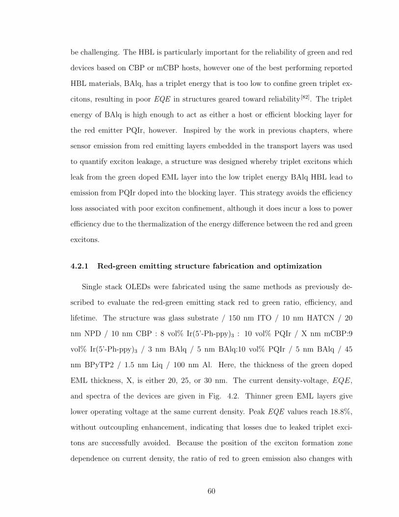
be challenging. The HBL is particularly important for the reliability of green and red
devices based on CBP or mCBP hosts, however one of the best performing reported
HBL materials, BAlq, has a triplet energy that is too low to confine green triplet ex-
citons, resulting in poor EQE in structures geared toward reliability [82]. The triplet
energy of BAlq is high enough to act as either a host or efficient blocking layer for
the red emitter PQIr, however. Inspired by the work in previous chapters, where
sensor emission from red emitting layers embedded in the transport layers was used
to quantify exciton leakage, a structure was designed whereby triplet excitons which
leak from the green doped EML layer into the low triplet energy BAlq HBL lead to
emission from PQIr doped into the blocking layer. This strategy avoids the efficiency
loss associated with poor exciton confinement, although it does incur a loss to power
efficiency due to the thermalization of the energy difference between the red and green
excitons.
4.2.1 Red-green emitting structure fabrication and optimization
Single stack OLEDs were fabricated using the same methods as previously de-
scribed to evaluate the red-green emitting stack red to green ratio, efficiency, and
lifetime. The structure was glass substrate / 150 nm ITO / 10 nm HATCN / 20
nm NPD / 10 nm CBP : 8 vol% Ir(5’-Ph-ppy)3 : 10 vol% PQIr / X nm mCBP:9
vol% Ir(5’-Ph-ppy)3 / 3 nm BAlq / 5 nm BAlq:10 vol% PQIr / 5 nm BAlq / 45
nm BPyTP2 / 1.5 nm Liq / 100 nm Al. Here, the thickness of the green doped
EML thickness, X, is either 20, 25, or 30 nm. The current density-voltage, EQE,
and spectra of the devices are given in Fig. 4.2. Thinner green EML layers give
lower operating voltage at the same current density. Peak EQE values reach 18.8%,
without outcoupling enhancement, indicating that losses due to leaked triplet exci-
tons are successfully avoided. Because the position of the exciton formation zone
dependence on current density, the ratio of red to green emission also changes with
60
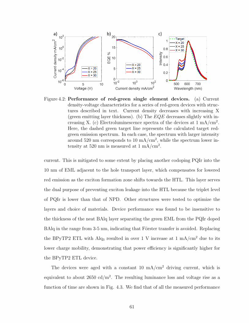
Figure 4.2: Performance of red-green single element devices. (a) Currentdensity-voltage characteristics for a series of red-green devices with struc-tures described in text. Current density decreases with increasing X(green emitting layer thickness). (b) The EQE decreases slightly with in-creasing X. (c) Electroluminescence spectra of the devices at 1 mA/cm2.Here, the dashed green target line represents the calculated target red-green emission spectrum. In each case, the spectrum with larger intensityaround 520 nm corresponds to 10 mA/cm2, while the spectrum lower in-tensity at 520 nm is measured at 1 mA/cm2.
current. This is mitigated to some extent by placing another codoping PQIr into the
10 nm of EML adjacent to the hole transport layer, which compensates for lowered
red emission as the exciton formation zone shifts towards the HTL. This layer serves
the dual purpose of preventing exciton leakage into the HTL because the triplet level
of PQIr is lower than that of NPD. Other structures were tested to optimize the
layers and choice of materials. Device performance was found to be insensitive to
the thickness of the neat BAlq layer separating the green EML from the PQIr doped
BAlq in the range from 3-5 nm, indicating that Forster transfer is avoided. Replacing
the BPyTP2 ETL with Alq3 resulted in over 1 V increase at 1 mA/cm2 due to its
lower charge mobility, demonstrating that power efficiency is significantly higher for
the BPyTP2 ETL device.
The devices were aged with a constant 10 mA/cm2 driving current, which is
equivalent to about 2650 cd/m2. The resulting luminance loss and voltage rise as a
function of time are shown in Fig. 4.3. We find that of all the measured performance
61
Figure 4.3: Lifetime of red-green single element devices. (left) Luminance overtime, normalized to the initial luminance. Extrapolated lifetime using thestretched exponential decay model, (i.e. L/L0 = exp[−(t/τ)β]) are shownas thin lines. (right) Voltage rise over time. Voltage rises faster for largerX.
characteristics, the red-to-green emission ratio was the strongest function of X. We
therefore set X = 25 nm in the red-green element for the SWOLED to most closely
match the target emission spectrum.
4.3 The blue emitting structure
The lifetime of the blue element is important to prevent color shift and a rapid
decrease in luminance with aging. We maximize blue device lifetime by using a graded
dopant profile and hot excited state management [32,83]. Dopant grading balances hole
and electron transport in the EML, resulting in a broadened exciton recombination
profile and reduced bi-molecular annihilation rates, compared to a similar device
with constant doping at the same brightness. Also, it was found that including the
deep blue phosphor mer-Ir(pmp)3 can ‘manage’ hot excited states, that is, reduce
the probability of a hot excited state degrading the host or emitter molecules [83].
The blue element only accounts for 15% of the initial luminance, so its degradation
impacts color shift more strongly than luminance loss. Increasing the lifetime of the
red-green element without increasing the blue element lifetime would accelerate color
shift with aging. The maximum allowable color shift depends on the application [84],
62

Figure 4.4: Performance of blue single element devices. (a) Current density-voltage characteristics. The blue device operating voltage is several voltshigher than for the red-green device. (b) The EQE characteristic for theblue PHOLEDs. Due to its low ηQY , Ir(dmp)3 based devices are limitedto ∼ 10% EQE . (c) Electroluminescence spectra of the devices.
Figure 4.5: Lifetime of blue single element devices. (left) Luminance over time,normalized to the initial luminance of 1000 cd/m2. The extrapolated T70lifetime is about 600 hrs. (b) Voltage rise over the same period.
and can also limit the useful device lifetime.
The optimized structure for a blue device incorporating graded doping and excited
state managers was reported in Nature Materials [83]. The single element blue device
structure was 70 nm ITO / 5 nm HATCN / 10 nm CPD / 20 nm mCBP:1814
vol% Ir(dmp)3 / 10 nm mCBP:1119 vol% Ir(dmp)3:3 vol% mer-Ir(pmp)3 / 20 nm
mCBP:128 vol% Ir(dmp)3 / 5 nm mCBP:8 vol% Ir(dmp)3 / 5 nm mCBP / 25 nm
Alq3 / 1.5 nm Liq / 100 nm Al. The performance of this structure is shown in Figs.
4.4 and 4.5.
63
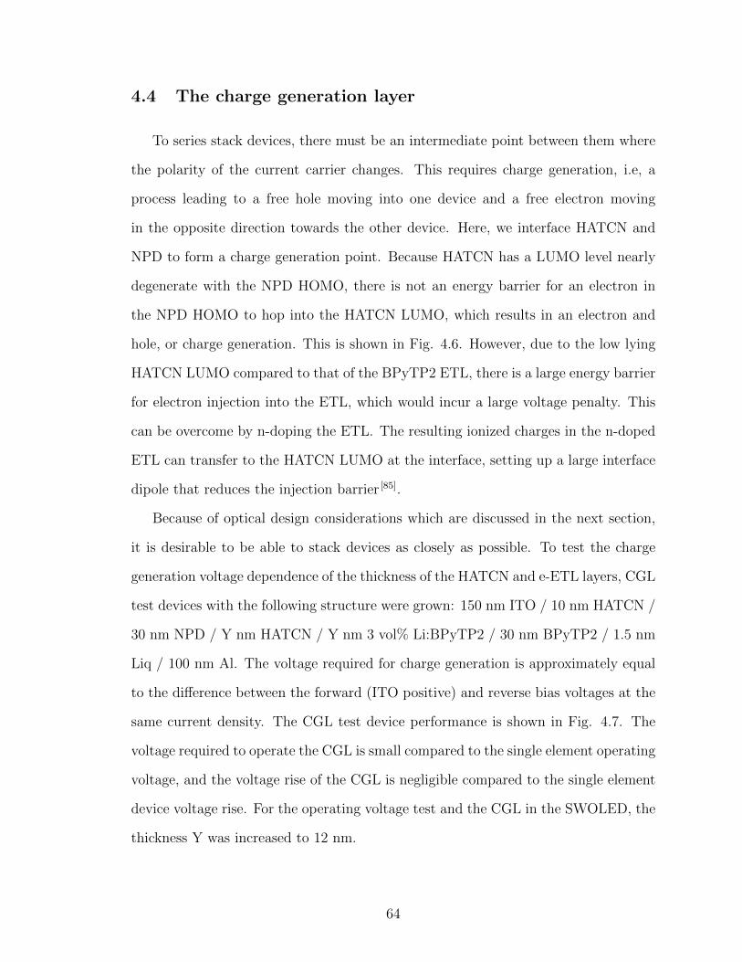
4.4 The charge generation layer
To series stack devices, there must be an intermediate point between them where
the polarity of the current carrier changes. This requires charge generation, i.e, a
process leading to a free hole moving into one device and a free electron moving
in the opposite direction towards the other device. Here, we interface HATCN and
NPD to form a charge generation point. Because HATCN has a LUMO level nearly
degenerate with the NPD HOMO, there is not an energy barrier for an electron in
the NPD HOMO to hop into the HATCN LUMO, which results in an electron and
hole, or charge generation. This is shown in Fig. 4.6. However, due to the low lying
HATCN LUMO compared to that of the BPyTP2 ETL, there is a large energy barrier
for electron injection into the ETL, which would incur a large voltage penalty. This
can be overcome by n-doping the ETL. The resulting ionized charges in the n-doped
ETL can transfer to the HATCN LUMO at the interface, setting up a large interface
dipole that reduces the injection barrier [85].
Because of optical design considerations which are discussed in the next section,
it is desirable to be able to stack devices as closely as possible. To test the charge
generation voltage dependence of the thickness of the HATCN and e-ETL layers, CGL
test devices with the following structure were grown: 150 nm ITO / 10 nm HATCN /
30 nm NPD / Y nm HATCN / Y nm 3 vol% Li:BPyTP2 / 30 nm BPyTP2 / 1.5 nm
Liq / 100 nm Al. The voltage required for charge generation is approximately equal
to the difference between the forward (ITO positive) and reverse bias voltages at the
same current density. The CGL test device performance is shown in Fig. 4.7. The
voltage required to operate the CGL is small compared to the single element operating
voltage, and the voltage rise of the CGL is negligible compared to the single element
device voltage rise. For the operating voltage test and the CGL in the SWOLED, the
thickness Y was increased to 12 nm.
64

Figure 4.6: Schematic operation of a charge generation test device. (Top)Forward bias operation (Vanode > Vcathode) injects charges from the con-tacts and results in charge recombination at the interior interface betweenNPD and HATCN. (bottom) Reverse bias operation (Vanode < Vcathode)results in charge generation at the interior interface between NPD andHATCN. The voltage difference to reach the same current density be-tween forward and reverse bias is approximately the voltage required togenerate the current. Energy levels are drawn assuming a flat vacuumlevel.
Figure 4.7: Operating voltage and lifetime of charge generation test devices.(a) Forward and reverse current density-voltage characteristics for differ-ent values of Y. Forward and reverse characteristics are shown in the samecolor, with reverse having lower current density at the same voltage. (b)Reverse minus forward voltage as a function of current. For Y = 10 nm,the CGL operating voltage at 1 mA/cm2 is less than 0.2 V. (c) Operat-ing voltage rise of the CGL devices under constant current load (reversebias).
65

4.5 Outcoupling considerations
As discussed in Sec. 1.2.2, the position of light generation in the organic material
impacts the coupling of light to the various modes. Using a Green’s function method,
we calculate the outcoupling efficiency vs position at wavelengths of 460, 520, 560, and
600 nm, see Fig. 4.8. Because substrate modes are relatively easy to outcouple using
microlens arrays or similar strategies, we also calculate the sum of power coupled
to air and substrate modes. At the first antinode, around 50 nm from the cathode,
the outcoupling maxima at different visible wavelengths are largely overlapping due
to the shared node at the cathode. However, at the second antinode, maxima for
the 460 nm and 600 nm wavelengths are spatially separated by about 70 nm. Thus,
by placing a red-green element at the first antinode, then the single blue element at
its second antinode, there is room to position a second red-green element near its
second antinode. Beyond this, wavelength dispersion causes the broad spectrum of
the red-green emitting element to no longer have a well defined antinode, especially
when considering both air and substrate modes.
4.6 Full SWOLED: structure and performance
The full structure of the SWOLED devices incorporating the red-green emitting,
blue emitting, and charge generation elements, is shown in Fig. 4.9. Devices having
three, four, or five total emissive elements are denoted D3-D5. Each device has a
single blue element combined with a varying number of red-green elements.
The J-V -luminance characterization used a semiconductor parameter analyzer
and a calibrated large area photodiode that collected all light exiting the bottom of
the glass substrate. For substrate-mode outcoupling measurements, IMF was placed
between the photodiode and substrate. The device output spectra were measured
using an integrating sphere coupled to a spectrometer. The J–V characteristics are
66
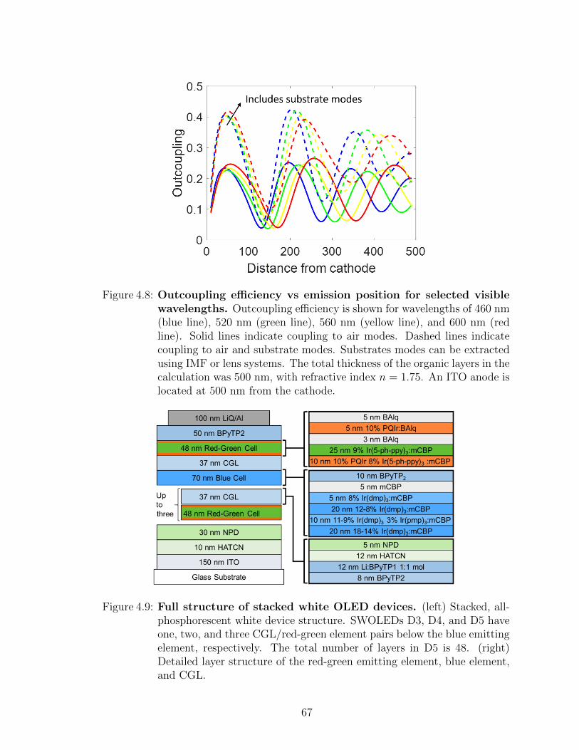
Figure 4.8: Outcoupling efficiency vs emission position for selected visiblewavelengths. Outcoupling efficiency is shown for wavelengths of 460 nm(blue line), 520 nm (green line), 560 nm (yellow line), and 600 nm (redline). Solid lines indicate coupling to air modes. Dashed lines indicatecoupling to air and substrate modes. Substrates modes can be extractedusing IMF or lens systems. The total thickness of the organic layers in thecalculation was 500 nm, with refractive index n = 1.75. An ITO anode islocated at 500 nm from the cathode.
Figure 4.9: Full structure of stacked white OLED devices. (left) Stacked, all-phosphorescent white device structure. SWOLEDs D3, D4, and D5 haveone, two, and three CGL/red-green element pairs below the blue emittingelement, respectively. The total number of layers in D5 is 48. (right)Detailed layer structure of the red-green emitting element, blue element,and CGL.
67

Figure 4.10: SWOLED J–V and efficiency characteristics. (left) The spectrumand current-density voltage characteristics of D3-D5. The voltage in-creases in regular steps with the number of red-green emitting elements.(right) EQE and luminance as functions of current density. Dashedlines represent quantities measured using IMF to outcouple all substratemodes.
given in Fig. 4.10(left). In the range J = 1-50 mA/cm2, the voltage increase when
adding additional red-green elements is 0.1-0.5 V less than the voltage of the red-green
test device (Fig. 4.2) at the same current-density. We conclude that the voltage drop
across the CGL is less than over the transport layers and contacts of the single EML
test devices. The EL spectrum of each device is also shown in Fig. 4.10. Devices D4
and D5 exhibit balanced red, green, and blue emission. The peak near 520 nm in the
D3 spectrum is blue-shifted by 10±1 nm compared to D4 and D5. There is also some
position and width variation in the peak near 610 nm. These differences are due to
changes in the cavity and the different outcoupling vs wavelength characteristics for
the different red-green element positions. The CCT, CRI, and 1931 CIE coordinates
of the spectra of fresh devices, as well as after aging to T70 are summarized in Table
4.1.
The EQE and luminance for D3-D5 are shown vs. J in Fig. 4.10(right). Here,
dashed lines were obtained by outcoupling substrate modes using IMF between the
device substrate and photodetector during the EQE measurement [86], leading to an
outcoupling improvement of 2.2±0.2 times over substrate emission without any out-
68

Table 4.1: Performance characteristics of SWOLEDs
CCT(a) CRI(a) CIE(a) J (b) V (b) EQE(b) LPE(b) T70(b)
(K) ( mAcm2 ) (V) (%) (lm/W) (103 h)
D3 2978 78.7 (0.44,0.40) 1.1 15.3 50.8 18.5 9± 2
/2518 /81.2 /(0.47,0.41) /0.5 /14.2 /107 /40.6 26± 7
D4 3300 85.1 (0.43,0.44) 0.9 19.3 57.7 19.1 15± 4
/2890 /85.2 /(0.46,0.43) /0.4 /17.8 /141 /47.2 50± 15
D5 2780 88.6 (0.46,0.43) 0.7 23.0 74.3 19.5 24± 5
/2420 /89.4 /(0.49,0.43) /0.3 /21.5 /170 /44.7 80± 20
(a) Measured at T100 / T70 and J = 10 mA/cm2
(b) Measured with no outcoupling / outcoupling at L0 = 1,000 cd/m2
coupling scheme. While simple outcoupling schemes such as microlens arrays give
smaller improvement factors (∼1.5) [87], similar improvements to that measured here
using IMF are achievable with other, deployable, wavelength independent outcoupling
schemes [86,88–91]. The EQE increases with the number of stacks, and assuming EQE
= 10% for the blue element without outcoupling [6,32], the average red-green element
EQE in D5 is 16.4±0.1%, which is slightly lower than for the single element red-green
test structure (18.0± 0.3%). Using IMF for substrate optical mode outcoupling, D5
reaches a maximum EQE = 171 ± 1% (averaging 34.2% EQE per stacked element)
and a luminance > 200, 000 cd/m2. The luminous power efficiency rolls off from
LPE = 50 ± 3 to 30 ± 2 lm/W (24 ± 2 lm/W to 13 ± 1 lm/W without IMF) as
the current-density increases from 0.1 to 10 mA/cm2, with an increasing number of
stacks tending to slightly increase the power efficiency.
Example spectra for D4, both fresh and aged to T70, are shown in Fig. 4.11.
The spectrum red shifts with aging due to the more rapid decrease in blue and green
emission relative to red. The angular emission intensity is shown in Fig. 4.11(left),
69
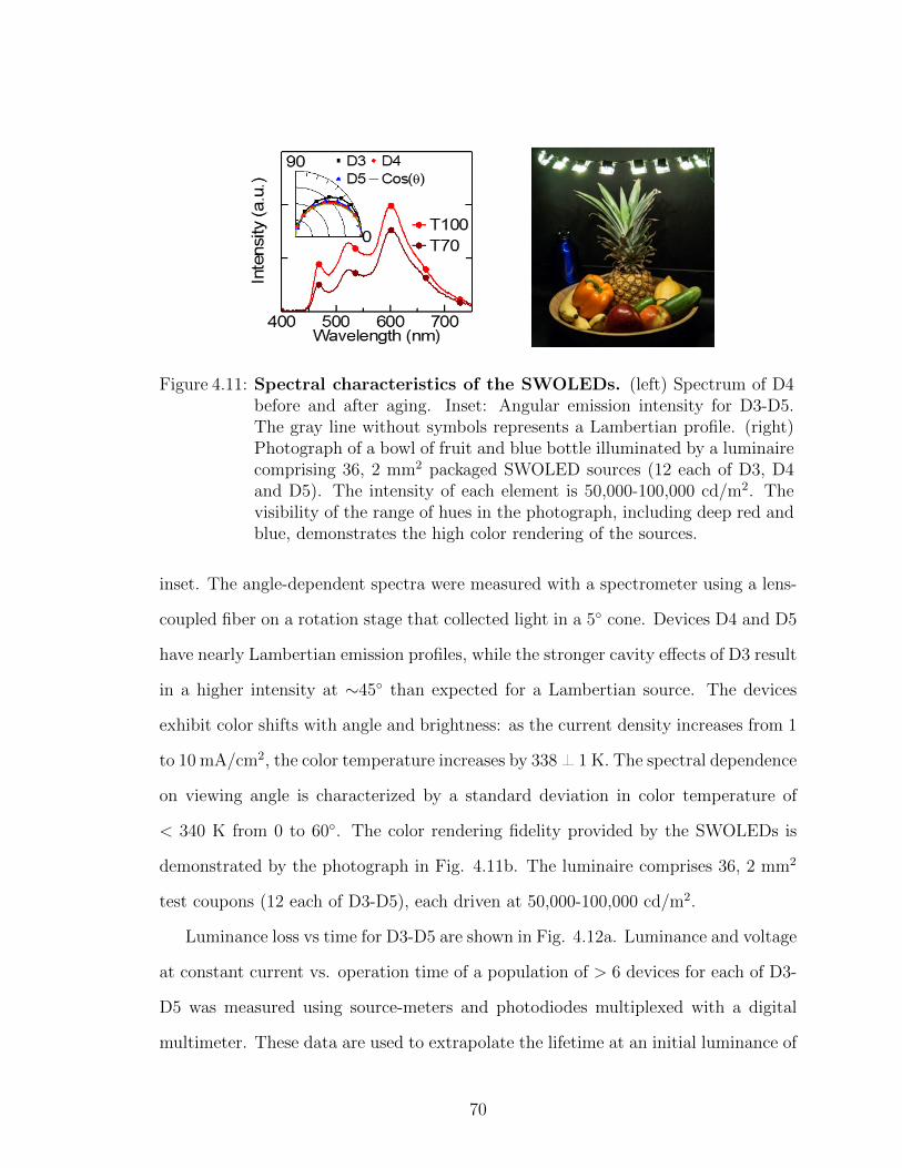
Figure 4.11: Spectral characteristics of the SWOLEDs. (left) Spectrum of D4before and after aging. Inset: Angular emission intensity for D3-D5.The gray line without symbols represents a Lambertian profile. (right)Photograph of a bowl of fruit and blue bottle illuminated by a luminairecomprising 36, 2 mm2 packaged SWOLED sources (12 each of D3, D4and D5). The intensity of each element is 50,000-100,000 cd/m2. Thevisibility of the range of hues in the photograph, including deep red andblue, demonstrates the high color rendering of the sources.
inset. The angle-dependent spectra were measured with a spectrometer using a lens-
coupled fiber on a rotation stage that collected light in a 5 cone. Devices D4 and D5
have nearly Lambertian emission profiles, while the stronger cavity effects of D3 result
in a higher intensity at ∼45 than expected for a Lambertian source. The devices
exhibit color shifts with angle and brightness: as the current density increases from 1
to 10 mA/cm2, the color temperature increases by 338± 1 K. The spectral dependence
on viewing angle is characterized by a standard deviation in color temperature of
< 340 K from 0 to 60. The color rendering fidelity provided by the SWOLEDs is
demonstrated by the photograph in Fig. 4.11b. The luminaire comprises 36, 2 mm2
test coupons (12 each of D3-D5), each driven at 50,000-100,000 cd/m2.
Luminance loss vs time for D3-D5 are shown in Fig. 4.12a. Luminance and voltage
at constant current vs. operation time of a population of > 6 devices for each of D3-
D5 was measured using source-meters and photodiodes multiplexed with a digital
multimeter. These data are used to extrapolate the lifetime at an initial luminance of
70

Figure 4.12: Lifetime characteristics of the SWOLEDs. (a) Normalized lumi-nance loss vs. time at current densities of J = 5, 10, 20, and 40 mA/cm2.At the same currents, luminance losses are reduced for devices with in-creasing numbers of stacked elements, which also have higher initial lu-minances. (b) Extrapolation of T70 vs. initial brightness. Error barsrepresent one standard deviation from a fit to the data using the relation:T70 × Ln0 = const, with n = 1.50 − 1.54. The dashed line correspondsto the initial luminance obtained using substrate mode outcoupling. (c)Operating voltage rise versus time at J = 5, 10, 20, and 40 mA/cm2.The voltage rises by 10-15% between T100 and T70.
1000 cd/m2 using the relationship T70×Ln0 = const, shown in Fig. 4.12b. The fitted
value of the exponent n is 1.50-1.54, and L0 is the initial brightness [92,93]. Because
outcoupling schemes result in higher luminance at the same current density, they also
result in longer lifetime at the same luminance, as shown by the dotted line for D5
in Fig. 4.12b. At L0 = 1000 cd/m2, T70 = 26 ± 7 khr, 50 ± 15 khr, and 80 ± 20
khr, for D3, D4, and D5, respectively. Error bars represent one standard deviation
in the extrapolated lifetime determined from the least squares fit. At the increased
luminance of L0 = 3000 cd/m2, T70 = 5± 1 khr, 10± 2 khr, and 14± 3 khr, for D3,
D4, and D5. Voltage rise data are shown in Fig. 4.12c. The 2.5 V to 4.5 V increase
in T70 for the devices represents 10-15% of the initial driving voltages. The constant
current testing of the CGL-only device (see Fig. 4.7), which shows that the voltage
rise contribution from the CGL is < 30 mV after > 250 hr at 30 mA/cm2, which is
longer than T70 of the device at the same drive current. This indicates that over 95%
of the voltage rise is due to aging of the layers comprising the SWOLEDs other than
the CGL. Device performance is summarized in Table 4.1.
71
4.7 Analysis of SWOLED performance
Stacking multiple elements lowers the current density required to reach a given
luminance, increasing the SWOLED lifetime and maximum brightness. Combining
red and green emitters into a single element improves the spectral control compared
to stacking separate red and green EMLs. Stacking also simplifies the design by
allowing for separate optimization of each emitting element. Large numbers of stacked
elements result in high voltage, low operating current devices. This is beneficial to
lifetime, which improves dramatically as current density is reduced (Fig. 4.12a). The
maximum number of stacks is determined by the allowable driving voltage or efficiency
considerations for a particular application. Indeed, we find that the maximum LPE
increases slightly with the number of stacks. Additionally, the lower current required
to achieve a given brightness reduces the efficiency roll-off, increasing power efficiency
at high luminance. The slight increase in power efficiency from D3 to D5 indicates
it is possible to further increase the number of stacks before resistive and absorption
losses significantly reduce the LPE.
The primary performance metrics for solid state lighting devices are the color
quality (CCT and CRI), power efficiency, and lifetime. The CRI is > 85 for both D4
and D5, with warm white CCTs. The power efficiency is 30-50 lm/W, which may
be improved by reducing operating voltage or better outcoupling. Ideally, this could
also be improved by using a high ηQY blue emitter, however we are limited by the
relatively poor reliability of most such molecules. Methods for decreasing operating
voltage include higher mobility hosts/dopants with smaller energy gap differences,
electron and hole conducting cohosts, and reducing the EML thickness. Also, separate
red and green EMLs can improve outcoupling, however more reliable structures are
required to realize these improvements without sacrificing lifetime.
To our knowledge, device lifetime of T70 = 80± 20 khr with L0 = 1000 cd/m2 is
the longest for white PHOLEDs with reported materials and structures. Lifetimes of
72
white PHOLEDs have been limited by rapid degradation of the blue EML, with T70 <
1 khr [83]. Blue fluorophores are therefore often used for their reliability in hybrid
fluorescent/phosphorescent white OLEDs [33]. However, the longest fully reported
hybrid fluorescent/phosphorescent device lifetime under the same test conditions of
which we are aware is 31 khr [94], which is less than half that of the PHOLEDs reported
here. This indicates that blue PHOLED lifetime, when increased by excited state
management, is sufficient for many lighting applications. Additionally, using CGLs
to stack EMLs and red-emissive blocking layers are crucial to achieving the long
SWOLED lifetimes reported here.
The small color shift of these devices with aging, shown in Fig. 4.11(left) and
Table 4.1, is achieved by the balanced degradation rates of the emitting elements.
The spectrum red-shifts slightly with time, due to the lower operational stability of
the blue element: when D5 reaches T70 the blue emission is decreased by 50%. At the
SWOLED T70, the blue cell loses about 5% more luminance without the hot excited
state manager, and 40% more luminance without either grading or hot excited state
manager.
4.8 Summary
In conclusion, we have demonstrated all-phosphorescent warm white, stacked
PHOLEDs with lifetime of T70 = 80 khr and a high CRI of 89. This is achieved
using three phosphors in five stacked EMLs comprising a device with a total of 48
layers. The device features red emissive blocking layers in the red-green element,
graded doping and hot excited state management in the blue element, and stable,
low voltage CGLs. These devices demonstrate the potential of white PHOLEDs for
solid state light sources. The design principles and strategies employed will undoubt-
edly lead to the further improvement of long lived SWOLEDs.
73
CHAPTER V
Centimeter-scale electron diffusion in photoactive
organic heterostructures
The unique properties of organic semiconductors are of fundamental interest while
being increasingly important to information displays, lighting, and energy generation.
However, organics suffer from both static and dynamic disorder that can lead to charge
conduction via variable-range carrier hopping [95,96]. This results in notoriously poor
electrical properties with electron and hole mobilities typically µ < 1 cm2/V-s and
correspondingly short charge diffusion lengths (LD =√Dτ < 1 µm), where D and τ
are the diffusivity and lifetime, respectively) [97,98]. These properties often constrain
organic optoelectronic devices which must be thin (∼ 100 nm), with continuous top
and bottom electrodes to avoid charge recombination and high resistance to lateral
transport within the organic layers. Here, we demonstrate an organic heterostructure
comprising a thin fullerene channel with significant photocurrent response to light
absorbed > 1 cm beyond its collecting contact. The channel is sandwiched between
an electron blocking layer and a blended donor:C70 HJ that generates charges by
dissociating excitons. The energy barrier between the channel and HJ confines elec-
trons to the fullerene layer, spatially separating them from photogenerated holes in
the HJ. As a result of this energetic confinement and exceptionally low trap densi-
74
ties within the channel and along its interfaces, centimeter-scale diffusion of electrons
is observed in the fullerene channel that can be fit with a simple electron diffusion
model. Our experiments enable the direct measurement of charge diffusivity in or-
ganic semiconductors, which is as high as D = 0.83 ± 0.07 cm2/s in a C60 channel
at room temperature. The high diffusivity of the fullerene combined with the ex-
traordinarily long charge recombination time yield LD > 3.5 cm, which is orders of
magnitude larger than expected for an organic system. The main conclusions of this
chapter were published in Nature [99].
5.1 Device fabrication
A series of devices was fabricated on 5 cm × 5 cm glass substrates containing four
pre-patterned indium tin oxide (ITO) strips (150 nm × 1 cm × 2.3 cm) as bottom
electrodes. Substrates were cleaned by sequential sonications in tergitol, deionized
water, acetone, and isopropanol followed by snow-cleaning [100] on a 100C hot plate
with a stream of gaseous CO2 and a 10 min UV-ozone exposure. The photoactive
device structure was 150 nm ITO / 10 nm MoOx / 80 nm donor:C70 1:1 / fullerene /
electron blocking layer / 100 nm Ag. The donor in the HJ was DTDCPB, DTDCTB,
SubPc, or DBP. The fullerene is either C60 or C70, and the electron blocker is either
an 8 nm thick layer of BPhen or a 10 nm thick layer of 1:1 BPhen:C60 with a 5 nm
thick BPhen cap. Mixed blocking layers are commonly used in OPVs to improve
stability and electron extraction efficiency [101,102].
Organic materials, metals, and MoOx were deposited at rates of 0.5-1 A/s through
shadow masks in a vacuum thermal evaporator at 10−7 Torr. Organics and MoOx
were deposited through a large square mask, leaving 1 mm of the substrate uncoated
around the periphery for electrical contacts to the ITO. Using a separate shadow
mask, 1 mm wide strips of 100 nm thick Ag films, were deposited across the organics
to form the cathode, with 0.1 cm2 of intersection perpendicular to the ITO bottom
75
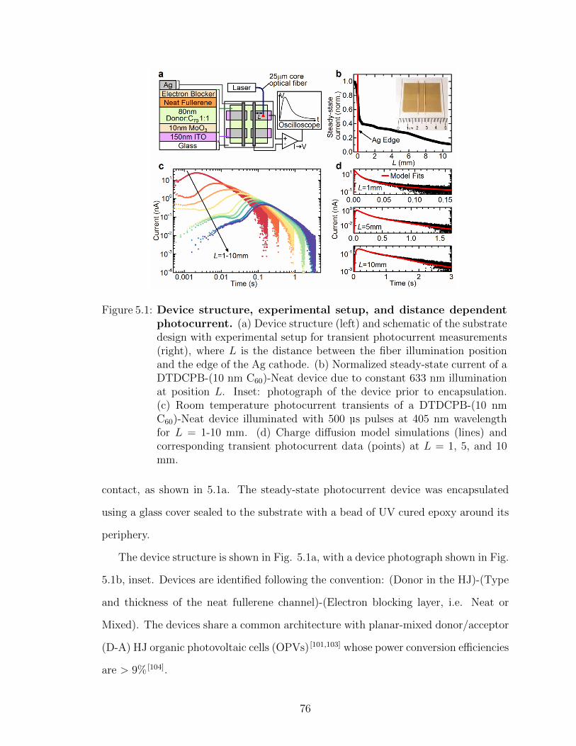
Figure 5.1: Device structure, experimental setup, and distance dependentphotocurrent. (a) Device structure (left) and schematic of the substratedesign with experimental setup for transient photocurrent measurements(right), where L is the distance between the fiber illumination positionand the edge of the Ag cathode. (b) Normalized steady-state current of aDTDCPB-(10 nm C60)-Neat device due to constant 633 nm illuminationat position L. Inset: photograph of the device prior to encapsulation.(c) Room temperature photocurrent transients of a DTDCPB-(10 nmC60)-Neat device illuminated with 500 µs pulses at 405 nm wavelengthfor L = 1-10 mm. (d) Charge diffusion model simulations (lines) andcorresponding transient photocurrent data (points) at L = 1, 5, and 10mm.
contact, as shown in 5.1a. The steady-state photocurrent device was encapsulated
using a glass cover sealed to the substrate with a bead of UV cured epoxy around its
periphery.
The device structure is shown in Fig. 5.1a, with a device photograph shown in Fig.
5.1b, inset. Devices are identified following the convention: (Donor in the HJ)-(Type
and thickness of the neat fullerene channel)-(Electron blocking layer, i.e. Neat or
Mixed). The devices share a common architecture with planar-mixed donor/acceptor
(D-A) HJ organic photovoltaic cells (OPVs) [101,103] whose power conversion efficiencies
are > 9% [104].
76

5.2 Measurement of lateral photocurrent
Using the experimental setup and device illustrated in Fig. 5.1a, the steady-state
photocurrent response of an OPV comprising the d-a-a’ DTDCTB blended with C60
was measured as a function of the excitation position under ∼ 0.15 mW/cm2 contin-
uous illumination at 633 nm through the substrate from a fiber-coupled He-Ne laser,
with results in Fig. 5.1b. In contrast to typical OPVs that exhibit no photoresponse
to light incident outside the area of overlap of their anode and cathode, the DTDCTB-
(10 nm C60)-Neat device generated a significant photoresponse to such illumination.
The magnitude of the steady-state photocurrent just outside the cathode was 40% of
the peak within the device, decreasing approximately linearly to 12% at L = 10 mm
away from the cathode edge, likely due to recombination or trapping at the film edge
where it contacted the encapsulation epoxy. The large drop in signal intensity at the
edge of the cathode originates from a decrease in light absorption due to the lack
of cathode reflection as well as a decrease in charge generation/collection efficiency
due to the lack of a built-in field outside of the contact area. The photocurrent gen-
erated outside the contact overlap, henceforth called “channel current,” can cause a
significant overestimation of the short-circuit current in an OPV when it is overfilled
by the illumination source [105]. Devices with DTDCPB as the donor also exhibited
channel currents, while those with SubPc or DBP as the donor had no response to
light outside the cathode edge.
Transient photocurrent measurements were performed under vacuum in an open-
loop liquid N2 cryostat with four vacuum feedthroughs for electrical contacts, optical
fiber, and micrometer fiber positioning arm. The 25 µm diameter core fiber with a
numerical aperture of 0.1, and a measured Gaussian output width of < 40 µm was
positioned normal to the device surface. Pulses (duration of 0.5 ms to 2 ms and delays
of 1 s to 100 s between pulses) from diode lasers (wavelengths 405 nm and 637 nm)
were focused into the fiber for temporal measurements. The position of the fiber was
77

controlled with an x-y-z micrometer positioning stage. A 99% optically absorptive
black foil was placed beneath the device to minimize light scattering. The current
response was amplified with a low-noise current amplifier at 108 V/A, and recorded
with a digital oscilloscope. Rise time filters between 10 µs and 10 ms were used on
the current amplifier to minimize noise, and all spectra were averaged over at least
10 pulses. The steady-state dark current was subtracted, leaving only the transient
response to the light pulses.
The transient behavior of channel currents in all device architectures was inves-
tigated, with 500 µs pulses of 405 nm wavelength light as the illumination source.
Figure 5.1c shows the transient channel current from the DTDCPB-(10 nm C60)-
Neat device illuminated at L = 1−10 mm. As L increased, the amplitude and arrival
time of the channel current varied by nearly two orders of magnitude, though the
standard deviation of the integrated charge collected for each transient was < 10% of
the mean for all transients. That is, we observe no measurable loss in the total number
of charges collected, independent of the position of excitation, indicating the charge
LD in the structure is considerably greater than the 1 cm device length. In devices
with C70 channels, the integrated signal decreased by 50% over 5 mm, suggesting
that LD is small compared with C60. The EQE (in this context, EQE = electrons
collected per incident photon) decreased as a function of pump pulse energy and du-
ration, presumably due to increased recombination at higher polaron concentrations.
In the DTDCTB-(10 nm C60)-Neat device at L = 2 mm, the EQE decreased from
30% to 15% as the pump pulse energy increased from 0.11 to 1.7 nJ at a wavelength
of 637 nm, and EQE decreased by 72% as the pulse length was increased from 0.1 to
100 ms. The collection efficiency of channel currents was wavelength independent, i.e.
it tracked the absorption spectrum of the blended HJ. Channel currents were only
observed when illuminating the organic area above the ITO anode, which was needed
to collect the photogenerated holes, thus preventing sample charging and reducing
78

recombination.
5.2.1 Fitting data with electron diffusion model
Charge dynamics were simulated from a solution to the diffusion equation,
d
dtN(x, y, t) = D∇2N(x, , y, t)− kN(x, y, t) +G(x, y, t), (5.1)
subject to blocking boundary conditions along the edges of the organic film and a
quenching boundary condition at the edge of the Ag cathode. Here, N is the electron
density, x is the distance from the cathode, y is the lateral position, t is the time, D
is the diffusivity, k is the sum of the trapping and recombination rates, and G is the
generation rate. Initially, N(x, y, 0) = 0. The generation term is given by
G(x, y, t) =Q
qtpulse
1
2πσ2
[(x− x0)2 + (y − y0)2
2σ2
], (5.2)
where Q is the charge injected into the fullerene transport layer, σ = 40 µm is the
laser beam diameter, (x0, y0) and tpulse are the position and length of the excitation,
respectively. The intrinsic carrier density in the fullerene layer is typically < 108 cm-3,
depending on the purity [106], which is many orders of magnitude below the optically
excited and electrically injected charge densities.
The current transient is given by the diffusion current into the cathode as a func-
tion of t:
I(t) = q
∫D
d
dxN(x, y, t)
∣∣∣∣x→0
dy. (5.3)
Equations 5.1-5.3 are solved numerically, and Eq. 5.3 is fit to the data with
parameters D, k, and Q. The diffusivity primarily determines the arrival time of the
current pulse and the slope of the falling edge, k determines the slope at long times,
and Q scales linearly with amplitude.
Due to the device symmetry and the blocking conditions on the perimeter of the
79

Table 5.1: Room temperature charge diffusion parameters extracted fromdistance-dependent transient current measurements
Device D k µ* Q
(cm2/s) (s-1) cm2/V-s (nC)
DTDCPB-(10 nm C60)-Neat 0.83± 0.07 0.9± 0.6 32± 3 2.2± 0.8
DTDCTB-(10 nm C60)-Neat 0.67± 0.06 1± 1 26± 2 0.32± 0.02
DTDCPB-(5 nm C60)-Neat 0.53± 0.03 0.4± 0.4 20± 1 0.35± 0.02
DTDCPB-(2 nm C60)-Neat 0.16± 0.02 0.7± 0.7 6± 1 0.29± 0.03
DTDCPB-(10 nm C60)-Mixed 0.37± 0.08 0.3± 0.2 14± 3 3.2± 0.8
DTDCPB-(10 nm C70)-Neat 0.16± 0.01 2.4± 0.8 6± 1 0.21± 0.02
*Estimated using the Einstein relation
organic films, diffusion parallel to the cathode interface does not affect the arrival
time of electrons at the cathode except in the case of diffusion around a cut in the
organic film. The simulated geometry is therefore one-dimensional in most cases,
simplifying computation.
This model was used to fit all transient currents as a function of L. Detailed
transients (points) from Fig. 5.1c plotted on a log-linear scale are shown for the
DTDCTB-(10 nm C60)-Neat device in Fig. 5.1d at L = 1, 5, and 10 mm. The
parameters extracted from the fits (lines) are given in Table 1. Among devices grown
in the same batch, DTDCTB and DTDCPB devices with 10 nm thick C60 channel
and neat electron blocking layers had comparable diffusivities, which were reduced
by replacing the C60 with C70, and by replacing the neat electron blocking layer
with a mixed layer. This reduction is presumably due to electron diffusion into the
mixed layer where D is relatively low. Decreasing the C60 channel thickness in the
DTDCTB-C60-Neat devices from 10 nm to 2 nm also decreased D and the amount
of total charge injected into the fullerene layer, Q. The peak-to-peak roughness
of the films grown on ITO is typically several nanometers as measured by atomic
force microscopy [107], thus the thin fullerene channels likely have discontinuities and
80

thickness variations that disrupt electron diffusion in thinner channels. The upper
bound for the rate of charge trapping and recombination, k, was about five times
larger in C70 compared with C60 channels. There were batch-to-batch variations in
D, k, and Q, but the relative performance between architectures was consistent, i.e.
devices with neat blockers or neat C60 always had considerably higher D than devices
with mixed blockers or C70 grown in the same batch.
5.2.2 Electron diffusion around a cut in the film
Room temperature transient currents were measured on a DTDCTB-(10 nm C60)-
Mixed device at L = 3 mm before and after a series of razor blade cuts was made to
the organic layers, as shown in the inset of Fig. 5.2. The peak height of the current
pulse was significantly reduced and the peak arrival time was delayed for devices
with a “partial cut” that was transverse to, and spanned the width of the ITO anode
between the illumination position and the Ag cathode, compared with the pristine,
uncut device. These results are shown in Fig. 5.2. Charge diffusion simulations were
performed for both geometries, where the only difference was a blocking boundary
condition at the position of the partial cut. We find that charge diffusion around
the cut accounts for the differences between the cut and uncut device transients, as
demonstrated by the remarkable agreement between fits (lines) and the data. The
partial cut was also extended such that there was no continuous organic path between
the illumination position and the cathode, called a ‘full cut’ device. This eliminated
the response except for a residual current at time, t < 200 ms arising from scattered
light absorbed in the organic layers between the cathode and cut. This effect was
observed in all devices exhibiting channel currents.
81

Figure 5.2: Impact of channel disruption on channel currents. Current tran-sients at L = 3 mm with a series of cuts, as shown in the inset. Diffusionmodel fits are shown for the uncut and partial cut geometries.
5.3 Frontier orbital energies of HJ and channel materials
UPS data were measured for donor:C70 blends both with and without a 5 nm C60
cap. The HOMO energies were measured under high vacuum (10−8 Torr) with a 21.2
eV photon source. Organic thin films were grown on conductive ITO substrates as
described above. The LUMO energies were estimated using the low energy optical
absorption edge of the material. The energy barrier between C70 in the donor:C70
blend and the neat C60 layer on top was estimated by measuring the binding energy
of the C70 HOMO in a 10 nm thick donor:C70 blend with a 5 nm thick C60 cap,
measuring the binding energy of the C60 HOMO and taking the difference between
these energies.
With the DTDCPB donor, we observe a 0.42 ± 0.1 eV difference between the
highest occupied molecular orbital (HOMO) energy (EHOMO) of the blended C70 and
neat C60 cap, whereas the difference in EHOMO between neat C60 and C70 is ∼ 0.1
eV. The difference in EHOMO between DBP:C70 blends with and without a 5 nm C60
82

Figure 5.3: Energetics of materials employed in devices. (a) Energy level di-agram extracted from ultraviolet photoelectron spectroscopy measure-ments on a 10 nm thick C70 and a 10 nm thick DTDCPB:C70 blendedfilm with and without a 5 nm thick C60 film grown on its surface. (b)Monte Carlo simulations of the hopping diffusion length as a function ofthe energy barrier height for electrons between the neat channel layer andthe donor-acceptor heterojunction. The dotted line indicates the lowerbound of the energy barrier measured via UPS.
cap was < 100 meV, indicating that DBP does not significantly shift EHOMO of C70
when the two constituents are blended. The energy levels are shown in Fig. 5.3.
To quantify the impact of the energy barrier between the fullerene channel and
HJ, we performed Monte Carlo simulations of the carrier transport within the device
structure to calculate LD, with results shown in Fig. 5.3b. Monte Carlo simulations of
charge diffusion were performed on a simple cubic lattice that contained 200×7×100
sites in the x, y, and z dimensions, respectively, with lattice constant a = 1 nm. Here,
x and y are the directions parallel to the substrate, while z extends vertically from the
substrate. Sites with z < 90a were designated as the donor:C70 blend, while the top
10 sites represented the neat fullerene channel. The blend was randomly generated,
with 50% of the sites occupied by fullerenes, corresponding to a 1:1 blend. Periodic
boundary conditions in y were used, with blocking interfaces at x = 0 (the periphery
of the organic films) and z = 100a (the interface between the fullerene channel and the
electron blocking layer). Quenching boundary conditions were assumed at z = 0 (the
MoOx/HJ interface) and x = 200a to collect electrons. Charges originating at (1, 1, 1)
83
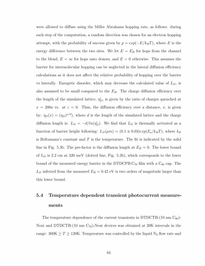
were allowed to diffuse using the Miller Abrahams hopping rate, as follows: during
each step of the computation, a random direction was chosen for an electron hopping
attempt, with the probability of success given by p = exp(−E/kBT ), where E is the
energy difference between the two sites. We let E = EB for hops from the channel
to the blend, E = ∞ for hops onto donors, and E = 0 otherwise. This assumes the
barrier for intermolecular hopping can be neglected in the lateral diffusion efficiency
calculations as it does not affect the relative probability of hopping over the barrier
vs laterally. Energetic disorder, which may decrease the calculated value of LD, is
also assumed to be small compared to the EB. The charge diffusion efficiency over
the length of the simulated lattice, η′D, is given by the ratio of charges quenched at
x = 200a vs. at z = 0. Thus, the diffusion efficiency over a distance, x, is given
by: ηD(x) = (ηD)x/d), where d is the length of the simulated lattice and the charge
diffusion length is: LD = −d/ln(η′D). We find that LD is thermally activated as a
function of barrier height following: LD(µm) = (0.1 ± 0.03)exp(Ea/kBT ), where kB
is Boltzmann’s constant and T is the temperature. The fit is indicated by the solid
line in Fig. 5.3b. The pre-factor is the diffusion length at EB = 0. The lower bound
of LD is 2.2 cm at 320 meV (dotted line, Fig. 5.3b), which corresponds to the lower
bound of the measured energy barrier in the DTDCPB:C70 film with a C60 cap. The
LD inferred from the measured EB = 0.42 eV is two orders of magnitude larger than
this lower bound.
5.4 Temperature dependent transient photocurrent measure-
ments
The temperature dependence of the current transients in DTDCTB-(10 nm C60)-
Neat and DTDCTB-(10 nm C70)-Neat devices was obtained at 20K intervals in the
range: 300K ≥ T ≥ 120K. Temperature was controlled by the liquid N2 flow rate and
84
a resistive heater, and monitored with a thermocouple. The results are shown in Figs.
5.4a and 5.4b at L = 2 mm and L = 1 mm, respectively. Each current transient was
fit using the charge diffusion model as shown by solid lines in Figs. 5.4c and 5.4d,
with the extracted values of D and k plotted vs. 1000/T in Figs. 5.4e and 5.4f.
Diffusion simulations successfully fit the data in Fig. 5.1 and 5.4 except at the
leading edge of the current transient. During measurement, some scattered light is
absorbed along the channel between the Ag edge and the intended point of photoexci-
tation, generating a prompt current response that is not accounted for by the model.
This response is delayed with increasing L, as can be seen in Fig. 5.1b, since the
scattered light is absorbed farther from the cathode, and bandwidth filters were used
to reduce noise on the low-amplitude spectra at larger L. Scattered light effects were
significantly suppressed by placing a highly absorptive foil beneath the device dur-
ing all measurements. The resistance-capacitance time constant of the measurement
circuit was < 100 ns and the amplifier rise-time was < 2 µs; both many orders of
magnitude shorter than the current response from the samples.
5.5 Electrically injected lateral diffusion device
As a check on the current measurements performed optically, electrically injected
lateral current devices were fabricated. The electrical injection device had the struc-
ture: p-type Si (20 Ω/) / 500 nm SiO2 / 10 nm BPhen / 50 nm C60 / 50 nm Ag
/ 20 nm DTDCPB:C70 1:1 / 8 nm BPhen / 100 nm Ag. The 50 nm thick Ag layer
(collecting contact), and the 100 nm thick Ag layer (injecting contact) were patterned
into 1 mm × 18 mm parallel strips using a shadow mask, separated by 1 cm. The
substrate oxide was etched in a small area away from the device to allow contact
with the Si using buffered HF. For alignment purposes, two electrically inactive Ag
strips positioned above the collecting contact were deposited simultaneously with the
injecting contact. We used the same HJ / channel / electron blocking layer structure
85
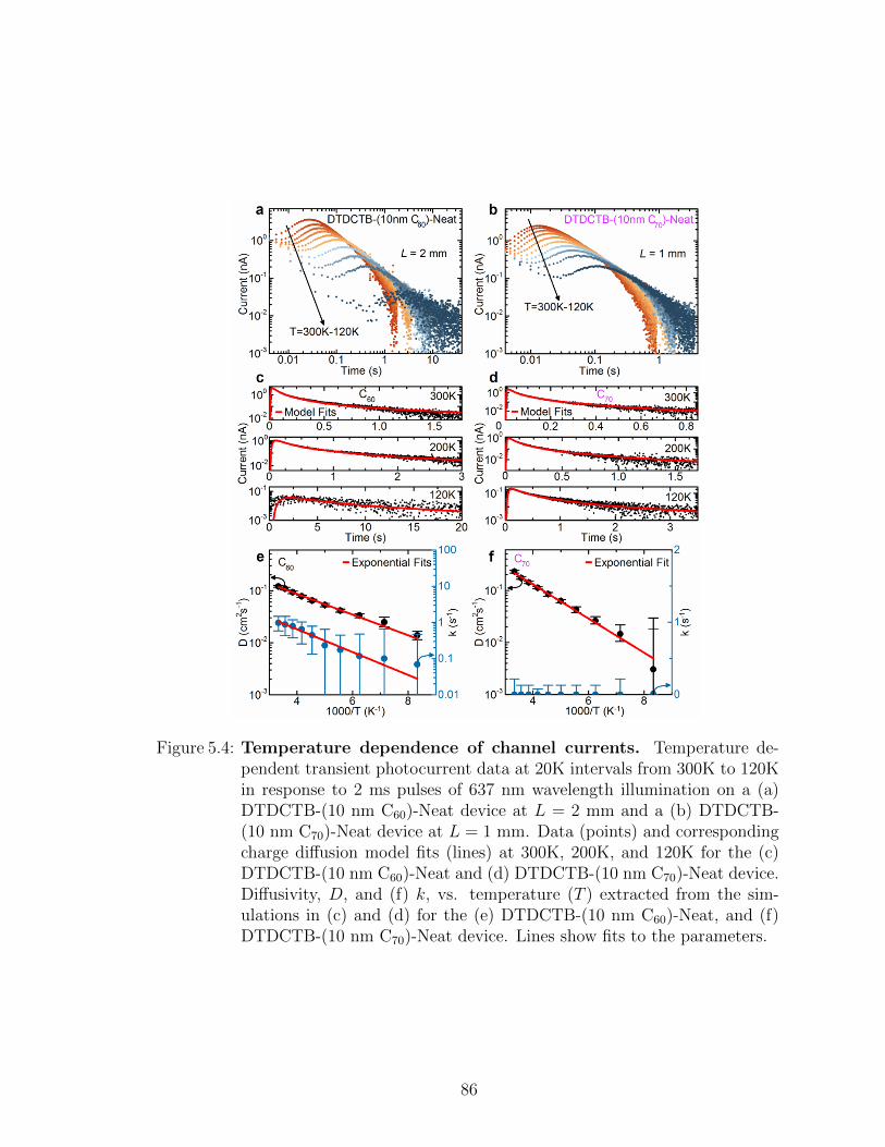
Figure 5.4: Temperature dependence of channel currents. Temperature de-pendent transient photocurrent data at 20K intervals from 300K to 120Kin response to 2 ms pulses of 637 nm wavelength illumination on a (a)DTDCTB-(10 nm C60)-Neat device at L = 2 mm and a (b) DTDCTB-(10 nm C70)-Neat device at L = 1 mm. Data (points) and correspondingcharge diffusion model fits (lines) at 300K, 200K, and 120K for the (c)DTDCTB-(10 nm C60)-Neat and (d) DTDCTB-(10 nm C70)-Neat device.Diffusivity, D, and (f) k, vs. temperature (T ) extracted from the sim-ulations in (c) and (d) for the (e) DTDCTB-(10 nm C60)-Neat, and (f)DTDCTB-(10 nm C70)-Neat device. Lines show fits to the parameters.
86
to enable a direct comparison between the electrical and optical devices, although
long-range diffusion is expected with any trap-free blocking interface. This structure
is shown schematically in Fig. 5.5a, with a photograph of the device in Fig. 5.5b,
inset.
Transient current measurements of the electrical injection device were performed
in the dark, under vacuum, and at room temperature. The Si substrate was grounded,
the injecting contact was connected to a pulse generator, and the current transient
at the collecting contact was measured with a current amplifier (107 V/A, 10 ms
rise-time filter) and digital oscilloscope. The results are shown in Fig. 5.5b. The
falling edge of the electrical injection device transient was also simulated using the
same diffusion model as above, where electrons were generated at a constant rate
beneath the injecting contact until a steady-state current was reached at the collecting
electrode. The collecting contact was placed at x = 0, with the edge of the injecting
contact at x = 1 cm. The parameters D and k measured for DTDCPB-(10 nm
C60)-Neat device in Table 5.1 were used in the calculation.
5.6 Analysis of results
The rates of trapping/recombination at defects and thermal emission into the HJ
where recombination can occur determine the lifetime of electrons in the channel.
A sufficiently high HJ energy barrier and low defect densities are therefore required
to enable transport over macroscopic distances. In devices with d-a-a’ donors, the
energy levels of C70 undergo a polarization shift due to the high dipole moments of
DTDCTB and DTDCPB (14.5 and 12.0 Debye, respectively) [104,108]. This shift forms
the required energy barrier at the C60 channel/HJ interface (0.42± 0.1 eV for DTD-
CPB, as shown in Fig. 5.3a) that confines electrons within the channel. Monte Carlo
simulations confirm that this barrier supports centimeter-scale diffusion, whereas in
DBP or SubPc donor devices with barrier heights < 100 meV have a much smaller
87
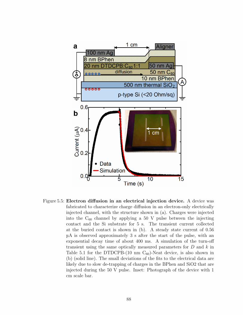
Figure 5.5: Electron diffusion in an electrical injection device. A device wasfabricated to characterize charge diffusion in an electron-only electricallyinjected channel, with the structure shown in (a). Charges were injectedinto the C60 channel by applying a 50 V pulse between the injectingcontact and the Si substrate for 5 s. The transient current collectedat the buried contact is shown in (b). A steady state current of 0.56µA is observed approximately 3 s after the start of the pulse, with anexponential decay time of about 400 ms. A simulation of the turn-offtransient using the same optically measured parameters for D and k inTable 5.1 for the DTDCPB-(10 nm C60)-Neat device, is also shown in(b) (solid line). The small deviations of the fits to the electrical data arelikely due to slow de-trapping of charges in the BPhen and SiO2 that areinjected during the 50 V pulse. Inset: Photograph of the device with 1cm scale bar.
88
LD < 5 µm. The centimeter-scale LD observed in devices with d-a-a’ donors suggests
that in addition to the large EB, the channel and its interfaces have a remarkably
low density of deep electron traps and recombination centers. This is surprising for
fullerenes, which, despite their unusually high mobility and diffusivity among molec-
ular solids [109–111], form disordered and phase-separated amorphous and crystalline
domains [112]. Long-range electron diffusion was also observed to circumvent barriers
introduced by physical cuts to the channel (Fig. 5.2), as well as in an electron-only
charge injecting sample (Fig. 5.5). Indeed, measurements of D and k in these exper-
iments are completely consistent with values obtained via photogeneration in Figs.
5.1 and 5.4. We note that drift-dominated charge lateral spreading drift of charges
over long time periods has been observed in single-carrier devices at organic/insulator
interfaces due to the lack of recombination [113]. Our results are inherently different
since the electron transport in our case is entirely diffusive. Here the surprising phe-
nomena is associated with the bulk, and is observed despite the presence of optically
generated minority carrier holes.
Replacing the 10 nm C60 layer with C70 reduces D from 0.67 ± 0.06 cm2/s to
0.16± 0.01 cm2/s at room temperature. The Einstein relation, D = µkBT/q, where
q is the electron charge, suggests that the larger D observed in the C60 devices is
consistent with its higher mobility [114,115]. This relation can also be used to estimate
the electron mobility of each device, as listed in Table 5.1, although we note that
D/µ in some organic systems has been shown to be larger than that predicted by the
Einstein relation due to disorder in the conduction site energies [116]. We find that the
room temperature mobilities, µ = 26± 3 cm2/V-s for C60 and 6± 1 cm2/V-s for C70,
are 2-5 times higher than those previously reported for fullerenes in transistors [109,110].
In general, mobilities in bulk semiconductors are larger than those at interfaces due to
interfacial traps [117,118], while mobilities and diffusivities in disordered semiconductors
typically increase with charge density due to filling of shallow traps and low-energy
89
states in the conduction band tail [119]. The devices measured here are therefore nearly
ideal for achieving high mobility, as charge transport occurs in the bulk of the channel
with electron densities > 1017 cm-3.
The diffusivities of DTDCTB-(10 nm C60)-Neat and DTDCTB-(10 nm C70)-Neat
devices are thermally activated with EA = 70 ± 8 meV and EA = 36 ± 3 meV
respectively (see Fig. 5.4e and 5.4f). The exponential decrease in D with temperature
is confirmation that conduction is limited by intermolecular hopping [120] even though
mobilities as high as those measured here are often attributed to band-like transport.
In the C70 device, k decreases as a function of temperature (EA = 50 ± 11 meV)
with nearly the same EA as D, suggesting that its Ld is approximately the mean free
path between collisions with sparsely distributed defects. In the C60 devices, best fits
give k < 0.1 s-1, which suggests that the electron lifetime is longer than the timescale
of the transient measurements. The values of D and k for C60 devices, therefore,
cannot be used to accurately predict LD. This is consistent with the fact that the
total charge collected in the transient measurements does not decrease systematically
with distance. However, we estimate an error of ∼ 25% in the amount of total
charge collected, thus a lower bound on diffusion length can be calculated using
exp(−1/LD) = 0.75, which yields LD > 3.5 cm.
5.7 Summary
Centimeter-scale electron diffusion is demonstrated in a photoactive, fullerene-
based heterostructure, with room temperature diffusivities of D = 0.67± 0.06 cm2/s
for C60 and D = 0.16 ± 0.01 cm2/s for C70, with thermal activation energies of
EA = 70 ± 8 meV and EA = 36 ± 3 meV, respectively. Among the structures ex-
plored, long-range diffusion was only observed when using d-a-a’ dipolar donors in the
photoactive D-A HJ adjacent to the electron conducting channel. The highly dipolar
donors destabilize the HOMO energy of C70 by 0.42± 0.1 eV in the blends, thereby
90
providing energetic confinement of electrons in the channel. Monte Carlo simulations
aided in understanding these results by confirming that even the lower bound of this
measured energy barrier (0.32 eV) is sufficient to support centimeter-scale diffusion in
the channel. The surprisingly long diffusion lengths suggest the nearly total absence
of recombination centers at interfaces or within the conducting fullerene channels,
even though the materials form disordered films. These results may prove useful
when applied in devices where long range charge transport is required. For exam-
ple, channel currents may open the possibility for organic optoelectronic devices with
unique properties, such as semi-transparent photovoltaics with large-period metal grid
cathodes, organic field effect transistors [121], and lateral photovoltaics [122]. Addition-
ally, energetically confined channels suggest that Hall-effect and lateral time-of-flight
experiments are possible for the accurate characterization of organic materials. How-
ever, the presence of such channels can also result in anomalously high short-circuit
currents during photovoltaic operation. In this circumstance, care must be taken to
prevent the overestimation of solar cell efficiency, particularly for small area devices
if the active area is overfilled by the illumination source.
91
CHAPTER VI
Organic charged-coupled devices
The demonstration of centimeter-scale lateral transport makes new types of or-
ganic devices possible. Perhaps the most common thin film lateral transport inor-
ganic semiconductor device is the CCD, which manipulates charge packets near a
semiconductor-insulator interface, allowing the charge packets to be passed between
closely spaced metal-oxide-semiconductor (MOS) capacitors. Since their conception
in 1970 [123,124], CCDs have been successfully applied to high sensitivity optical imag-
ing, and are valued for their excellent signal-to-noise ratio, high quantum efficiency,
linearity, and speed [125,126]. Because practical sensors require charges to transport lat-
erally across millimeter-to-centimeter distances for imaging, CCDs based on organic
semiconductors have not been practical due to their typically low charge diffusivi-
ties and short carrier lifetimes. However, the recent demonstration of efficient charge
transport across distances of several centimeters in organic thin film heterostruc-
tures using energetic barriers to physically separate electron and hole polarons [99],
as described in Ch. V, opens the possibility for realizing organic charge-coupled
devices (OCCDs).
Here, we demonstrate an OCCD that transfers photogenerated electron packets
across a 1.78 cm long, linear, three-phase shift register. Reaching the end of the reg-
92
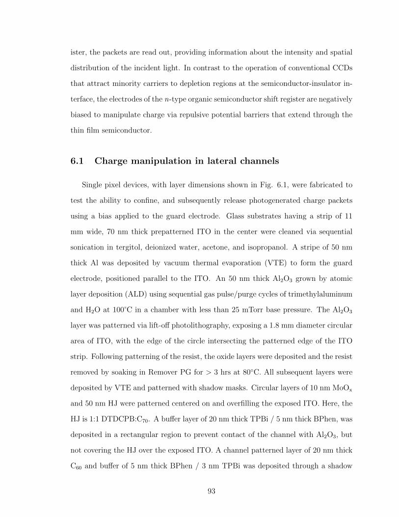
ister, the packets are read out, providing information about the intensity and spatial
distribution of the incident light. In contrast to the operation of conventional CCDs
that attract minority carriers to depletion regions at the semiconductor-insulator in-
terface, the electrodes of the n-type organic semiconductor shift register are negatively
biased to manipulate charge via repulsive potential barriers that extend through the
thin film semiconductor.
6.1 Charge manipulation in lateral channels
Single pixel devices, with layer dimensions shown in Fig. 6.1, were fabricated to
test the ability to confine, and subsequently release photogenerated charge packets
using a bias applied to the guard electrode. Glass substrates having a strip of 11
mm wide, 70 nm thick prepatterned ITO in the center were cleaned via sequential
sonication in tergitol, deionized water, acetone, and isopropanol. A stripe of 50 nm
thick Al was deposited by vacuum thermal evaporation (VTE) to form the guard
electrode, positioned parallel to the ITO. An 50 nm thick Al2O3 grown by atomic
layer deposition (ALD) using sequential gas pulse/purge cycles of trimethylaluminum
and H2O at 100°C in a chamber with less than 25 mTorr base pressure. The Al2O3
layer was patterned via lift-off photolithography, exposing a 1.8 mm diameter circular
area of ITO, with the edge of the circle intersecting the patterned edge of the ITO
strip. Following patterning of the resist, the oxide layers were deposited and the resist
removed by soaking in Remover PG for > 3 hrs at 80C. All subsequent layers were
deposited by VTE and patterned with shadow masks. Circular layers of 10 nm MoOx
and 50 nm HJ were patterned centered on and overfilling the exposed ITO. Here, the
HJ is 1:1 DTDCPB:C70. A buffer layer of 20 nm thick TPBi / 5 nm thick BPhen, was
deposited in a rectangular region to prevent contact of the channel with Al2O3, but
not covering the HJ over the exposed ITO. A channel patterned layer of 20 nm thick
C60 and buffer of 5 nm thick BPhen / 3 nm TPBi was deposited through a shadow
93

Figure 6.1: Single pixel device dimensions. The ITO is prepatterned (extent ofthe ITO is not shown to scale). Subsequent layer deposition order is Alguard, Al2O3 (not shown, it covers everywhere except the circular area ofthe bottom buffer), MoOx and HJ, bottom buffer, channel and top buffer,then cathode. All units are in mm.
mask. Finally, a 50 nm thick, 0.5 mm wide stripe Ag cathode was deposited parallel
to and spaced 0.3 mm from the insulated guard electrode, on the side opposite the
ITO. Devices were encapsulated using a glass cover slide sealed to the substrate with
a bead of UV cured epoxy around its periphery in a N2 environment with < 1 ppm
water and O2. A desiccant (CaO) was included inside device packages.
These devices are shown schematically in Fig. 6.2a. As with the devices in Ch.
V, which have a similar organic layer structure, charges are generated at the HJ when
illuminated, with holes collected at the anode. The generated electrons are energet-
ically confined to the C60 channel, where they laterally diffuse to the Ag cathode,
which is connected to a transimpedance amplifier and are subsequently detected by
94
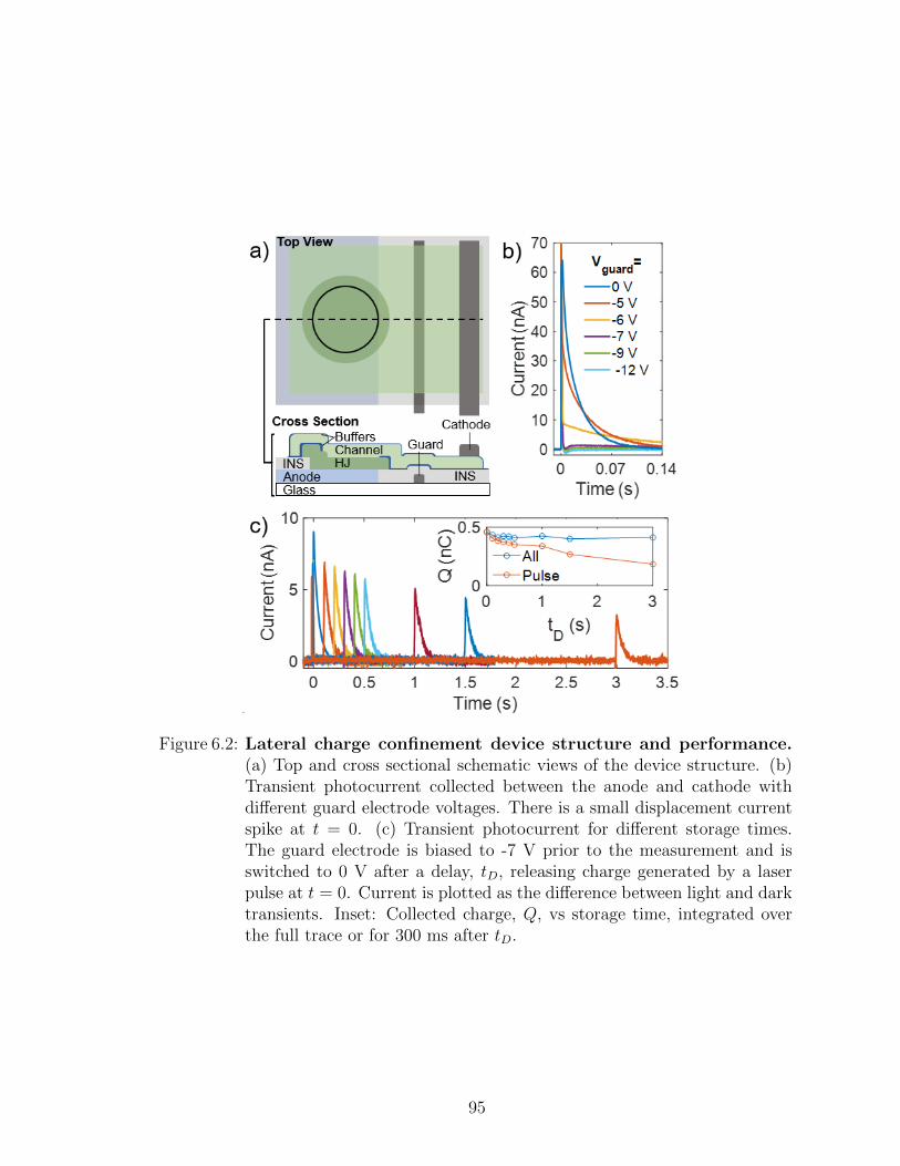
Figure 6.2: Lateral charge confinement device structure and performance.(a) Top and cross sectional schematic views of the device structure. (b)Transient photocurrent collected between the anode and cathode withdifferent guard electrode voltages. There is a small displacement currentspike at t = 0. (c) Transient photocurrent for different storage times.The guard electrode is biased to -7 V prior to the measurement and isswitched to 0 V after a delay, tD, releasing charge generated by a laserpulse at t = 0. Current is plotted as the difference between light and darktransients. Inset: Collected charge, Q, vs storage time, integrated overthe full trace or for 300 ms after tD.
95
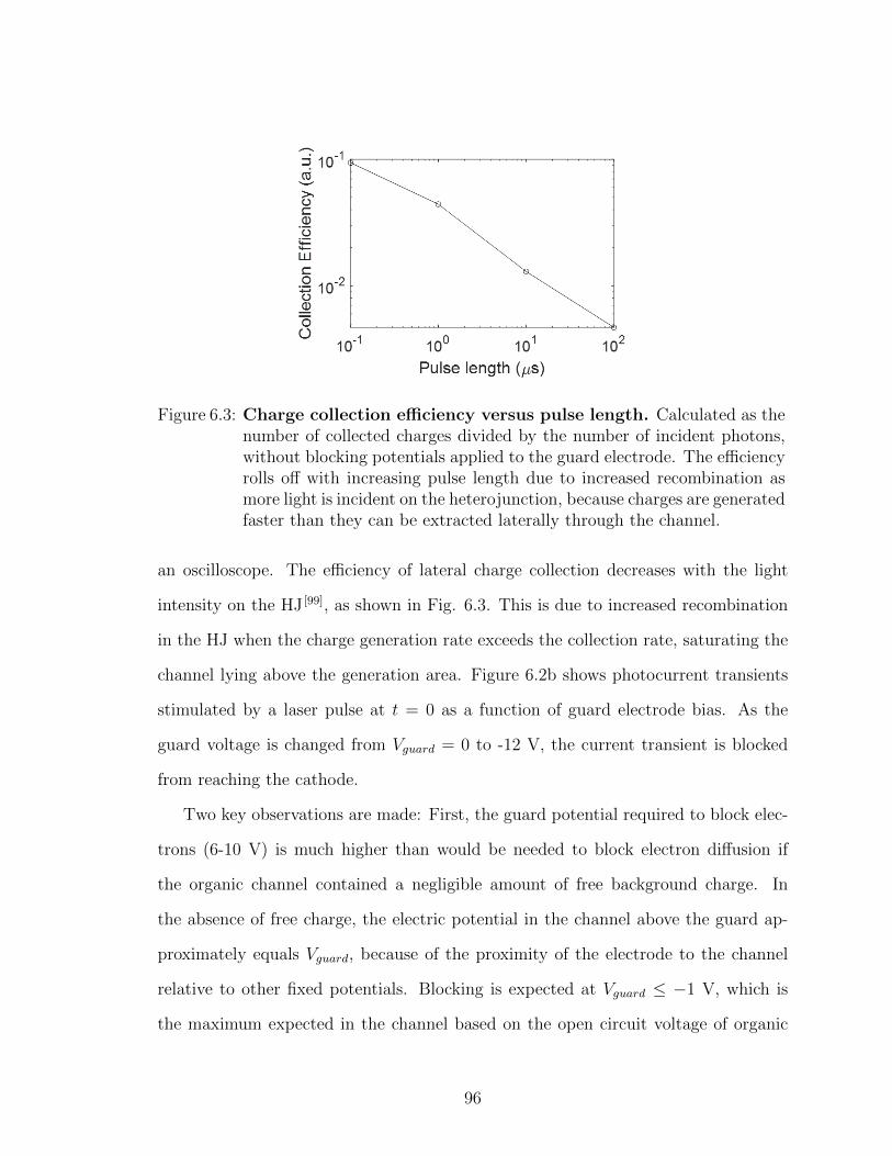
Figure 6.3: Charge collection efficiency versus pulse length. Calculated as thenumber of collected charges divided by the number of incident photons,without blocking potentials applied to the guard electrode. The efficiencyrolls off with increasing pulse length due to increased recombination asmore light is incident on the heterojunction, because charges are generatedfaster than they can be extracted laterally through the channel.
an oscilloscope. The efficiency of lateral charge collection decreases with the light
intensity on the HJ [99], as shown in Fig. 6.3. This is due to increased recombination
in the HJ when the charge generation rate exceeds the collection rate, saturating the
channel lying above the generation area. Figure 6.2b shows photocurrent transients
stimulated by a laser pulse at t = 0 as a function of guard electrode bias. As the
guard voltage is changed from Vguard = 0 to -12 V, the current transient is blocked
from reaching the cathode.
Two key observations are made: First, the guard potential required to block elec-
trons (6-10 V) is much higher than would be needed to block electron diffusion if
the organic channel contained a negligible amount of free background charge. In
the absence of free charge, the electric potential in the channel above the guard ap-
proximately equals Vguard, because of the proximity of the electrode to the channel
relative to other fixed potentials. Blocking is expected at Vguard ≤ −1 V, which is
the maximum expected in the channel based on the open circuit voltage of organic
96

Figure 6.4: Background charge transients. (Left) Device schematic and detectioncircuit. (Top right) Displaced background charge signal. (Bottom right)Total displaced charge versus Vguard. The amount of charge displacedrolls off with the onset of photocurrent blocking, which for this sampleoccurred between 12-14 V.
photovoltaic devices using the same HJ materials [127]. Large displacement current
transients due to the capacitance between the channel and guard electrode are mea-
sured when switching Vguard, shown in Fig. 6.4 together with the measurement circuit
and displaced channel. These transients saturate with the onset of charge blocking.
They are due to background mobile charge in the channel. Integrating the displaced
charge when switching Vguard from 0 to -7 V gives 2± 1 nC, corresponding to a back-
ground charge density of 1.2± 0.6× 1012 cm-2 if the area above the electrode is fully
depleted under bias.
Second, the measurement should be taken promptly after switching to Vguard <
0 V. This bias condition attracts positive charge that accumulates at the organic-
insulator interface, shielding the C60 channel from the guard potential, see Fig. 6.5.
97

Figure 6.5: Positive charge accumulation. (a) Photograph and cross sectionalschematic of a modified single pixel device. (B) Transient guard voltage.The potential on the guard ring relaxes to roughly half its initial value on atimescale determined by the light level and exposure area. (C) Equivalentcircuit model.
The data in Fig. 6.5 is taken using a modified single pixel device, pictured in Fig.
6.5a. Here, the guard electrode forms a ring surrounding the exposed ITO area, and
is insulated on the top and bottom by 50 nm ALD Al2O3 layers. The MoOx / HJ
layers were deposited through the same mask as the channel, and the top Ag cathode
forms a partial ring enclosing the guard electrode. The HJ, buffer, and channel layer
compositions are unchanged from those described above. The guard electrode was
left floating, with its voltage measured using a high impedance buffer amplifier (> 1
TΩ). At t = 0 the guard voltage was briefly (< 20 ms contact time) set to -6 V. This
was carried out in the dark, at two different ambient light levels, and in the light with
a mask that confined exposure to the center of the guard ring.
The measurement result can be explained using the equivalent circuit shown in
Fig. 6.5c. The guard electrode capacitance is composed of two parts, the capacitance
98
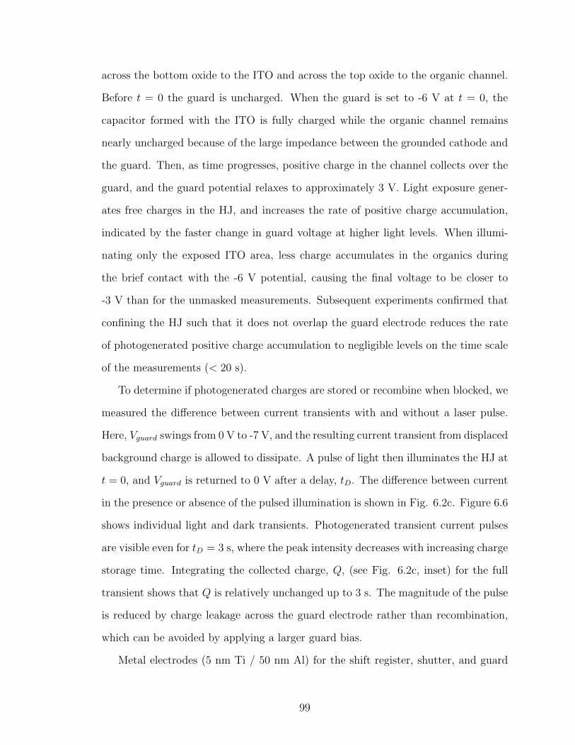
across the bottom oxide to the ITO and across the top oxide to the organic channel.
Before t = 0 the guard is uncharged. When the guard is set to -6 V at t = 0, the
capacitor formed with the ITO is fully charged while the organic channel remains
nearly uncharged because of the large impedance between the grounded cathode and
the guard. Then, as time progresses, positive charge in the channel collects over the
guard, and the guard potential relaxes to approximately 3 V. Light exposure gener-
ates free charges in the HJ, and increases the rate of positive charge accumulation,
indicated by the faster change in guard voltage at higher light levels. When illumi-
nating only the exposed ITO area, less charge accumulates in the organics during
the brief contact with the -6 V potential, causing the final voltage to be closer to
-3 V than for the unmasked measurements. Subsequent experiments confirmed that
confining the HJ such that it does not overlap the guard electrode reduces the rate
of photogenerated positive charge accumulation to negligible levels on the time scale
of the measurements (< 20 s).
To determine if photogenerated charges are stored or recombine when blocked, we
measured the difference between current transients with and without a laser pulse.
Here, Vguard swings from 0 V to -7 V, and the resulting current transient from displaced
background charge is allowed to dissipate. A pulse of light then illuminates the HJ at
t = 0, and Vguard is returned to 0 V after a delay, tD. The difference between current
in the presence or absence of the pulsed illumination is shown in Fig. 6.2c. Figure 6.6
shows individual light and dark transients. Photogenerated transient current pulses
are visible even for tD = 3 s, where the peak intensity decreases with increasing charge
storage time. Integrating the collected charge, Q, (see Fig. 6.2c, inset) for the full
transient shows that Q is relatively unchanged up to 3 s. The magnitude of the pulse
is reduced by charge leakage across the guard electrode rather than recombination,
which can be avoided by applying a larger guard bias.
Metal electrodes (5 nm Ti / 50 nm Al) for the shift register, shutter, and guard
99
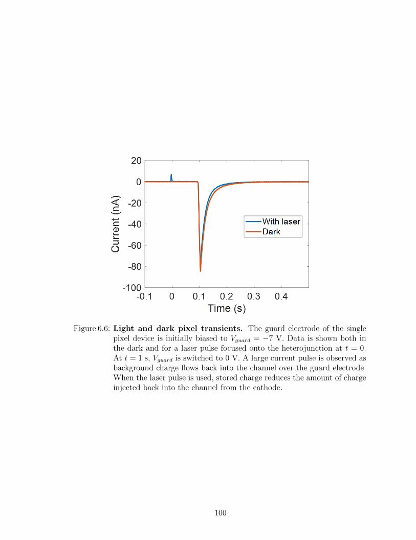
Figure 6.6: Light and dark pixel transients. The guard electrode of the singlepixel device is initially biased to Vguard = −7 V. Data is shown both inthe dark and for a laser pulse focused onto the heterojunction at t = 0.At t = 1 s, Vguard is switched to 0 V. A large current pulse is observed asbackground charge flows back into the channel over the guard electrode.When the laser pulse is used, stored charge reduces the amount of chargeinjected back into the channel from the cathode.
100
were patterned on a glass substrate by photolithography and covered with 50 nm
ALD Al2O3 (masking contact pad areas using a gel strip). Next, the Ag anode (as
with all subsequent layers) was patterned with a shadow mask and deposited by VTE.
Then MoOx and HJ layers were patterned into four squares over the anode, aligned
with every third shift register electrode. Next, a bottom buffer of 20 nm TPBi / 5
nm BPhen was deposited covering the periphery of the heterojunction and the full
shift register. Then, a 20 nm C60 channel and 5 nm BPhen / 3 nm TPBi top buffer
layers were deposited, slightly underfilling the shift register and covering the HJs,
with 1 mm wide interconnects between each HJ and the shift register area. The Ag
cathode was deposited over the channel and top buffer layers where they extend past
the guard electrode. Mask dimensions are given in Fig. 6.7.
The four-pixel OCCD is shown schematically in Fig. 6.8a. Of the 13 insulated
electrodes, 11 define the shift register and one each forms the guard and shutter
electrodes. A Ag anode runs parallel to the shutter electrode on the side opposite
the shift register. The three shift register phases are denoted Φ1−Φ3. The electrode
nearest the guard electrode is Φ1, followed by Φ2, Φ3, Φ1, etc. (see Fig. 6.8a). A
photograph of the device is shown in Fig 6.8b.
Photocurrent is collected between the anode and cathode in response to illumi-
nation of the HJ without biasing the electrodes. This current can be cut off by
biasing any one of the shutter, guard, or Φ1 electrodes (at < −8 V), since they
completely bisect the channel connecting the HJs to the cathode. We demonstrate
charge coupled transport by first biasing Φ2, Φ3, and shutter electrodes to -10 V, and
Vguard = −8.75 V. This expels charge from the channel above the biased electrodes,
leaving background charge packets confined above Φ1. The shift register is clocked
using a three-phase scheme shown in Fig. 6.9a-b, advancing the charge packets to-
ward the cathode. The first few steps of this process are shown schematically in Fig.
6.9a. Because Vguard > −10 V, charges diffuse towards the cathode when expelled
101
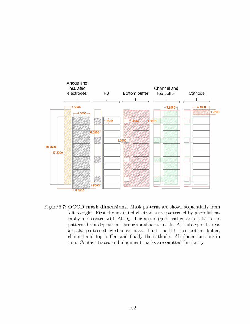
Figure 6.7: OCCD mask dimensions. Mask patterns are shown sequentially fromleft to right: First the insulated electrodes are patterned by photolithog-raphy and coated with Al2O3. The anode (gold hashed area, left) is thepatterned via deposition through a shadow mask. All subsequent areasare also patterned by shadow mask. First, the HJ, then bottom buffer,channel and top buffer, and finally the cathode. All dimensions are inmm. Contact traces and alignment marks are omitted for clarity.
102
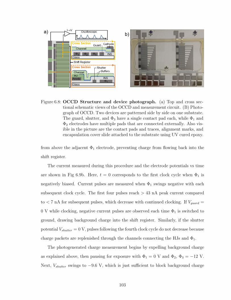
Figure 6.8: OCCD Structure and device photograph. (a) Top and cross sec-tional schematic views of the OCCD and measurement circuit. (B) Photo-graph of OCCD. Two devices are patterned side by side on one substrate.The guard, shutter, and Φ3 have a single contact pad each, while Φ1 andΦ2 electrodes have multiple pads that are connected externally. Also vis-ible in the picture are the contact pads and traces, alignment marks, andencapsulation cover slide attached to the substrate using UV cured epoxy.
from above the adjacent Φ1 electrode, preventing charge from flowing back into the
shift register.
The current measured during this procedure and the electrode potentials vs time
are shown in Fig 6.9b. Here, t = 0 corresponds to the first clock cycle when Φ1 is
negatively biased. Current pulses are measured when Φ1 swings negative with each
subsequent clock cycle. The first four pulses reach > 43 nA peak current compared
to < 7 nA for subsequent pulses, which decrease with continued clocking. If Vguard =
0 V while clocking, negative current pulses are observed each time Φ1 is switched to
ground, drawing background charge into the shift register. Similarly, if the shutter
potential Vshutter = 0 V, pulses following the fourth clock cycle do not decrease because
charge packets are replenished through the channels connecting the HJs and Φ1.
The photogenerated charge measurement begins by expelling background charge
as explained above, then pausing for exposure with Φ1 = 0 V and Φ2, Φ3 = −12 V.
Next, Vshutter swings to −9.6 V, which is just sufficient to block background charge
103

Figure 6.9: OCCD readout scheme and signal. (a) Schematic diagram of poten-tial sequence for electrodes at the end of the shift register. Here, sequentialsnapshots of the electrode potentials are shown at times t1− t3. High po-tentials repel the electron charge packets, indicated as shaded areas. (b)Top: Measured signal from expulsion of background charge, as describedin the text. Bottom: voltage vs time for Φ1-Φ3 during the measurement.Current pulses are measured each time Φ1 swings negative. (b) Mea-sured signal for dark and single pixel illumination exposures. Here, t = 0corresponds to the first time Φ1 swings negative following exposure.
104
from leaking into the shift register during a single clock cycle in the dark. Then, one
HJ is illuminated with a λ = 637 nm wavelength laser, generating charges and raising
the potential of electrons in the channel. This increases the rate of electrons leaking
from the illuminated HJ over the shutter. Following exposure, Vshutter is switched
back to -12 V and the shift register is emptied by a series of eight clock cycles. Figure
6.9c shows the measured current in the dark, and with illumination focused onto one
pixel per measurement, resulting in a distinct current pulse observed at a time delay
corresponding to the illuminated pixel.
Using majority carrier electrons to store information represents a significant dif-
ference from conventional CCD architectures that transfer minority carriers. Using
majority carriers precludes using attractive potentials (positive electrode bias, in the
case of electrons) to confine charge packets because no depletion region would form.
Additionally, the shift register and photoactive regions are spatially separated, since
extracting photogenerated holes from the HJ requires circuit connectivity that pre-
vents depletion. This scheme is general and is also applicable to inorganic devices.
Conventional CCD architectures are also suitable for OCCDs provided they use long-
range lateral diffusion structures for minority carriers or charge depleted channels.
Vacuum deposited films of pre-purified C60 have been reported to be weakly n-
type, with background charge densities ranging from 107− 1011 cm-3 [128–130] and esti-
mated donor densities of 1014 cm-3 [128]. The charge density measured here corresponds
to 4±2×1017 cm-3 if the background charge is confined within the channel, and likely
includes effects from unintentional bulk [128–130] or interface doping [131,132]. Blocking
via repulsive potentials is achieved once the channel above the electrode is depleted of
background charge. Reducing the background charge density, for example by further
purification of the materials, is therefore expected to reduce the voltage required to
block the lateral current. The minimum blocking voltage may be limited by energetic
disorder leading to tail states in the distribution of transport sites, which likely plays
105
a role in the charge leakage over the blocking potentials, as shown in Fig. 6.2c.
The four large current pulses in Fig. 6.9b correspond to the four charge packets
over the Φ1 electrodes. The small subsequent pulses are due to residual background
charges in the regions between electrodes as well as imperfect transfer of the photo-
generated charge. These parasitic signal pulses can be reduced by overlapping the
electrodes to eliminate the intervening spaces, and optimization of phase potential
waveforms. Variations in the magnitude of the first four pulses is likely a result of
nonuniformities in fabrication, the transfer process at the first and last pixel, and the
phase waveforms. The reduction in pulse magnitude after the fourth pulse confirms
charge coupled transport.
The transfer rate between adjacent electrodes is approximated from the solution to
the drift-diffusion equation, n(x, t) = D∇2n(x, t)−µFx∇n(x, t), subject to boundary
conditions δxn(L, t) = µFxn(L, t) and n(0, t) = 0, which correspond to perfect charge
blocking and extraction, respectively. Here, n is the charge density, D = 0.8 cm2s-1 is
the electron diffusivity and µ = 30.8 cm2/v-s the mobility (obtained from the Einstein
relation at room temperature) [99], and L is the pixel width. Also, Fx is the lateral
electric field in the channel that we assume is constant for simplicity, i.e. we neglect
self-repulsion and the spatial dependence of fringe fields [133]. The time required for
99.99% charge transfer between adjacent electrodes, tCT , is shown in Fig. 6.10 as a
function of electric field. The readout time for an N × N matrix of pixels (N 1)
using a three-phase clock scheme is tRO ≈ tCT (3 × N)2/Namp, where Namp is the
number of readout amplifiers. In the diffusion limit, a 500 × 500 pixel sensor with
Namp = 4 requires 6-7 micron pixels to achieve tRO < 1 s, while 10 micron pixels
and Namp = 500 (1 per column) yields tRO < 20ms. Introducing drift transport
significantly decreases tRO, for example by fringing fields as shown in Fig. 6.10, inset.
This analysis neglects charges trapped at defects or in the tail of the transport density
of states, which may reduce the charge transfer speed and collection efficiency.
106

Figure 6.10: Simulated charge transfer time versus pixel dimension. Thetransfer time, tCT , is calculated from the solution to the drift-diffusionequation using D = 0.8 cm-1 and µ = 30.8 cm-1s-1 as the time at which99.99% of the initial uniform charge distribution has transferred to theadjacent electrode. Blocking and zero density boundary conditions, aswell as a uniform electric field, are assumed. The inset shows the conceptof drift-inducing fringing fields and direction of the lateral field.
Despite the inherently lower charge mobility in organic compared to inorganic
semiconductors, OCCDs have the advantage of being potentially less difficult to man-
ufacture in flexible, ultralight, and large area form factors, which could potentially
be of use in simplifying complex optical systems. Organic CCDs may be especially
compelling for space applications, where their low weight [134,135], low sensitivity to cos-
mic radiation [136,137], and reduced requirements for encapsulation are advantageous.
They can function as an element in ultralight optical imaging systems when used
with thin film Fresnel lenses [138], or as lightweight memory devices. Additionally,
stacked, semi-transparent OCCDs with spectrally resolved absorption characteristics
could have near 100% pixel fill factor in each color and generate color images without
color filters.
107

6.2 Summary
We have demonstrated a charge coupled device comprising an organic semicon-
ductor thin film deposited on a series of closely spaced, insulated electrodes. Charge
coupled transport is demonstrated for both thermally and photogenerated charge
packets. The packets are confined using repulsive potentials, which contrasts with
conventional inorganic semiconductor CCDs that transport minority carriers using a
staircase of attractive potentials. This work demonstrates the versatility of organic
semiconductors and paves the way for further development of high performance OC-
CDs. These may find use is imaging applications where their flexible, ultralight form
factors and other attributes of organic semiconductors (e.g. radiation hardness) are
required.
108

CHAPTER VII
Future work
7.1 Future work: OLEDs
7.1.1 Reliability
Important areas for the further development of OLED technology include increas-
ing their power efficiency and reliability. Of these, reliability was the primary focus
of the work presented in this thesis. The reliability of blue PHOLEDs is one of the
most important remaining challenges. Based on studies of blue phosphorescent de-
vice degradation [6,42,67], and including Ch III of this work, intrinsic degradation of the
emissive layer materials in blue emitting devices limits their useful lifetime. Strate-
gies involving device structure [32] and reducing the intrinsic degradation due to hot
states [83] have proven effective for improving blue lifetime. However, substantial fur-
ther progress will likely require new chemicals for both host and dopant, incorporating
strong intra-molecular bonds and appropriate energy levels to reduce molecular disso-
ciation. Growth methods for reducing morphological changes during operation, such
as aggregate formation and crystallization, may also yield reliability improvements.
109

7.1.2 Power efficiency
One promising route for reaching the thermodynamic limit for power efficiency is
the use of exciplex-forming cohost systems [139–141]. This strategy avoids energy loss
due to difference between the transport level offset and the exciton energy. Energy
transfer from exciplexes directly to phosphors additionally avoids exchange energy
losses, or the difference in the singlet and triplet exciton energies. One example
device using this scheme is shown in Fig. 7.1. In this device, a single electron
transporting, exciplex forming cohost material and three sequentially layered hole
transporting, exciplex forming cohost materials form the host structure for the EML.
The HOMO-LUMO offset of each pairing of the electron transporting host with the
hole-transporting hosts is matched to the triplet energy of a red, green, or blue phos-
phor. Thus, injected carriers which recombine in red, green, or blue emitting regions
have transport gaps nearly equal to the emission energy of the dopants in those re-
gions. Cohosts are ordered such that no carrier has an exothermic hopping step
when transporting through the device to avoid thermalization losses. Because it
avoids energy loss from exciton relaxation, this structure has a theoretical power ef-
ficiency higher than hybrid fluorescent/phosphorescent white devices and traditional
all-phosphorescent devices, such as those presented in Ch. IV. Devices employing a
single hole transporting host with multiple electron transporting hosts, other permu-
tations of host combinations, and stacked single-color exciplex-cohost devices are also
possible. Additionally, conductivity-doped transport layers and injection or blocking
layers may be used with this scheme to realize an OLED near the thermodynamic
limit for power efficiency.
7.1.3 Charge balance and exciton confinement
There are additional areas to be explored using the methods for understanding
charge balance presented in Ch. II-III. New chemicals and architectures will likely
110
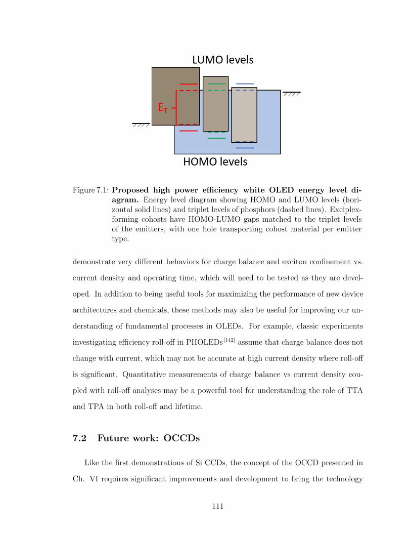
Figure 7.1: Proposed high power efficiency white OLED energy level di-agram. Energy level diagram showing HOMO and LUMO levels (hori-zontal solid lines) and triplet levels of phosphors (dashed lines). Exciplex-forming cohosts have HOMO-LUMO gaps matched to the triplet levelsof the emitters, with one hole transporting cohost material per emittertype.
demonstrate very different behaviors for charge balance and exciton confinement vs.
current density and operating time, which will need to be tested as they are devel-
oped. In addition to being useful tools for maximizing the performance of new device
architectures and chemicals, these methods may also be useful for improving our un-
derstanding of fundamental processes in OLEDs. For example, classic experiments
investigating efficiency roll-off in PHOLEDs [142] assume that charge balance does not
change with current, which may not be accurate at high current density where roll-off
is significant. Quantitative measurements of charge balance vs current density cou-
pled with roll-off analyses may be a powerful tool for understanding the role of TTA
and TPA in both roll-off and lifetime.
7.2 Future work: OCCDs
Like the first demonstrations of Si CCDs, the concept of the OCCD presented in
Ch. VI requires significant improvements and development to bring the technology
111
to a mature stage. Developing OCCDs has the advantage of using the development of
conventional CCDs as a road map, however new and unique challenges specific to the
organic devices will require innovation. Important areas for the further development
of OCCDs, listed in a suggested order of priority, include: control over background
charge density through doping and material purification, pixel-scaling, integrated
readout circuitry, drift-transport schemes, and stacked semitransparent arrays. Each
of these is addressed briefly below.
7.2.1 Controlling background charge density
Control over doping density for both electrons and holes in silicon CCDs has
been essential to their success. For example, the doping density is directly related
to the charge capacity-per-area of the pixels, and both n and p-type dopants are
needed for buried-channel devices [125]. The electrode voltages and device structure in
the OCCD demonstrated in Ch. VI were in large part dictated by the background
charge density. Understanding the origin of and controlling the background charge
density will be important to making higher performance devices. Experiments of
interest include measuring the background charge density vs. material purity (or
number of thermal gradient sublimation steps), intentional channel doping using n
and p-dopants (for example lithium and MoOx), as well as material surveys to test
alternative buffer layers that may contribute to the the background charge density
via interfacial doping. Additionally, hole conducting channels should be possible,
and might be of use in OCCDs if the mobilities are comparable or higher than for
electrons. Materials combinations for p-type channels should have similar energetics
to n-type channels, i.e, the channel HOMO should be shallow compared to the HOMO
levels in the HJ and buffer layers. Channel mobility might be best determined using
electrical injection structures such as in Fig. 5.5.
112

Figure 7.2: Diagram of OCCD electrodes. Electrodes are separated from theorganic channel by an insulator layer of uniform thickness. Insulatorlayers of a similar thickness prevent shorting between adjacent electrodes,which are overlapping. Note that the drawing is not to scale: electrodewidths are micron-scale while organic and insulator layer thicknesses arenanometer-scale.
7.2.2 Pixel-scaling
There are a number of considerations when scaling OCCD pixel size and number.
First, micron-scale gaps between adjacent shift register electrodes are not acceptable
in high performance devices, especially with pixel dimensions < 100 microns. Indeed,
practical devices require electrode spacings on the order of the insulator thickness, as
shown in Fig. 7.2. This scheme of overlaping adjacent electrodes significantly reduces
potential wells and barriers between electrodes, and should improve charge transfer
efficiency.
Additionally, high charge transfer efficiency becomes increasingly important as
the number of pixels (and therefore transfer steps) increases. The amount of charge
remaining in a charge packet after n transfers scales as (ηCTE)n. The fractional
amount of charge remaining in a charge packet after n transfer steps is shown in Fig.
7.3 for various values of ηCTE. Extremely high charge transfer efficiency is required
to maintain signal intensity over the millions of transfers required for a megapixel
sensor. Energetic disorder of transport sites and interface or bulk traps pose a serious
concern– no electron may be left behind when transferring charge packets. This may
place an upper limit on both readout speed and the number of pixels OCCDs can
113

Figure 7.3: Charge packet integrity vs number of transfers. The amount ofcharge remaining in the original charge packet decreases with each transferwhen ηCTE < 1. Lost charge is smeared out behind the original packet,degrading the signal integrity of subsequent charge packets.
achieve. It is therefore necessary that ηCTE be well characterized for practical OCCDs.
7.2.3 Integrated readout circuitry
In Ch VI, charge packets were measured using a current amplifier. While this
is adequate for the large (mm) pixel sizes and slow (ms) transfer times, high per-
formance devices require special purpose, integrated readout circuitry. Indeed, a
significant portion of the research and development of Si CCDs has been devoted to
low noise, low capacitance readout structures. Two styles of readout sensors used
for conventional inorganic CCDs, floating diffusion and floating gate amplifiers, are
pictured in Fig. 7.4. Both styles amplify a voltage shift at the gate of the transistor
connected in series with a gain resistor Rgain, producing a signal at Vout. A constant
VDD is applied to the drain of the readout transistor to power the amplifier. In the
case of the floating gate (Fig. 7.4a), charge diffusing out of the shift register is directly
collected onto the (temporarily floating) electrode, causing a voltage shift. After mea-
surement, the electrode bias is reset to V− by pulsing Vreset to briefly turn on the reset
114

Figure 7.4: Readout amplifiers styles. (a) A floating diffusion amplifier. Here,the electrode is biased at V− to attract signal charge. The reset transistoris then turned off and a charge packet is released from the shift register,which diffuses to the electrode. The amount of charge and the capacitanceof the electrode determine the voltage shift after collecting the chargepacket. The voltage shift is measured by a second transistor in serieswith a gain resistor. Finally, Vreset is pulsed to turn the reset transistor onbriefly to reset the electrode potential in preparation for reading the nextcharge packet. (b) A floating gate amplifier. Biasing the set electrodeto Vset capacitively biases the sense electrode. The sense electrode ispatterned in the out-of-page direction and connected to the insulatedgate of the transistor. Charge packets passing under the sense electrodecause its potential to decrease, producing an amplified signal at Vout.
transistor, preparing the amplifier for the next charge packet. Rather than coming at
the end of the shift register, the floating gate amplifier [143] (Fig. 7.4b) replaces one
of the shift register electrodes. The set electrode is biased to Vset, which capacitively
couples to the sense electrode. Charge packets passing through the channel near the
sense electrode change its potential, generating a signal. Because the transistor gate
is insulated, the sense electrode is always floating, and its potential is modified ca-
pacitively, without a change in net charge. Unlike the destructive measurement by
the floating diffusion method, the floating gate amplifier preserves the charge packet
after measurement, allowing a single charge packet to be measured multiple times.
The capacitance of the amplifier input is inversely related to the voltage change
per signal electron, requiring fF scale amplifier capacitance for high gain (∼µV/e).
Organic thin film transistors are process compatible with OCCD fabrication steps
and may find use in these readout circuits.
115
7.2.4 Drift-transport schemes
Charge transfer speed can be increased compared to a purely diffusive system
by introducing a lateral field and drift transport. Shift register electrode structures
for applying lateral fields in OCCDs include thick insulator, many electrode, and
resistive-sheet electrode structures. Each is described below.
7.2.4.1 Thick insulator scheme
Increasing the insulator thickness relative to the electrode dimension causes the
potential of a charge-neutral channel to deviate from the underlying electrode po-
tentials. This introduces lateral field across the channel over an electrode when the
adjacent electrodes have different potentials. An example of this is shown in Fig.
7.5. To calculate the channel potential, Laplace’s equation ∇2V = 0 is solved in two
dimensions on a rectangular area. The potential on the side of interest, which cor-
responds to the electrodes of the shift register, is a stepwise function determined by
the electrode biases along the length of the shift register, while the remaining three
boundaries are set to 0 V and placed L = 5 µm away from the region of interest,
where L is the length of an electrode. For this example, a single 5 µm electrode is
placed symmetrically about x = 0, with very wide ( 5 µm) electrodes on either
side. The leftmost electrode is biased at 1 V, the central electrode is biased at 0.5
V, and the right electrode is set to 0 V. The channel potential in the absence of free
charge is taken as the potential along a line parallel to electrode boundary, offset by
a variable insulator thickness. For insulators 5 µm, the channel potential approx-
imates the electrode potential at the same lateral position. As the oxide thickness
increases, the channel potential blurs and the potential slope (lateral field) over the
center of the 5 µm pixel increases. This scheme has the disadvantage of reduced
charge capacity-per-area due to the thick insulator layer.
116
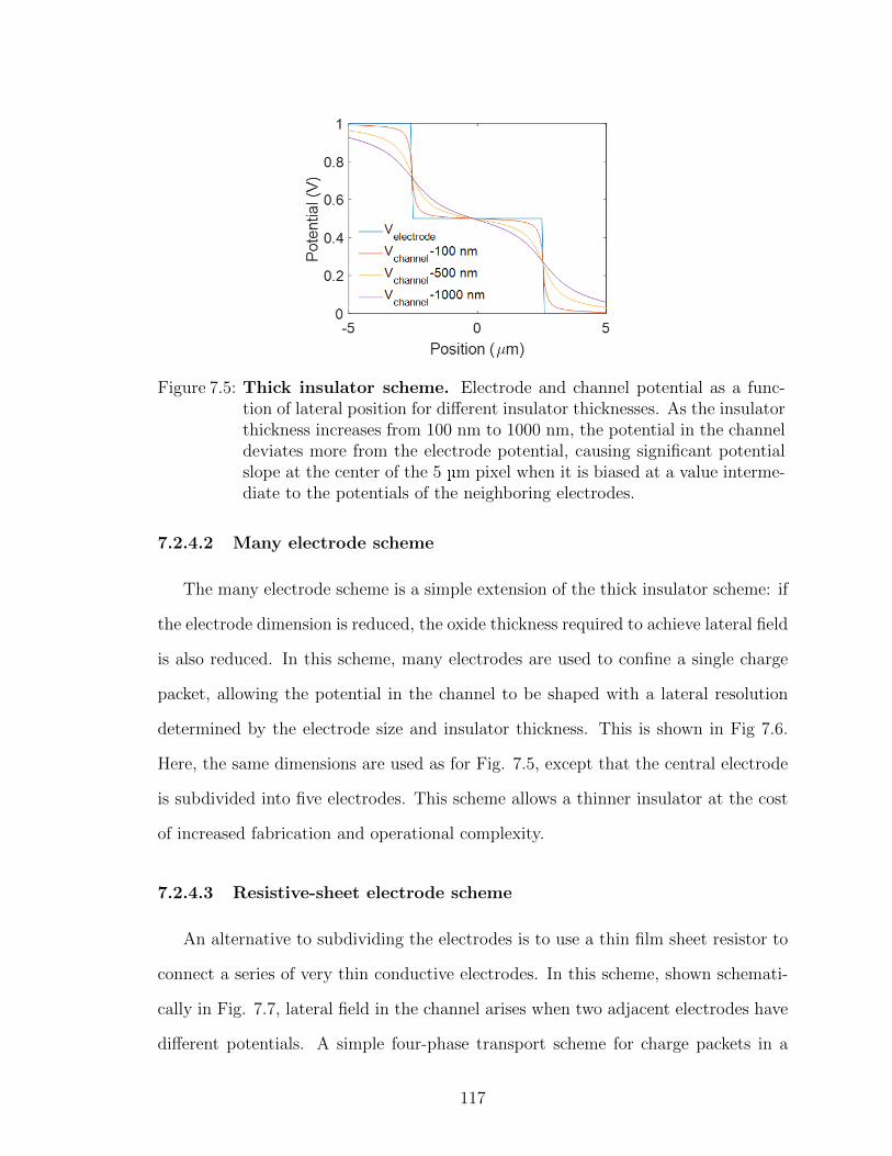
Figure 7.5: Thick insulator scheme. Electrode and channel potential as a func-tion of lateral position for different insulator thicknesses. As the insulatorthickness increases from 100 nm to 1000 nm, the potential in the channeldeviates more from the electrode potential, causing significant potentialslope at the center of the 5 µm pixel when it is biased at a value interme-diate to the potentials of the neighboring electrodes.
7.2.4.2 Many electrode scheme
The many electrode scheme is a simple extension of the thick insulator scheme: if
the electrode dimension is reduced, the oxide thickness required to achieve lateral field
is also reduced. In this scheme, many electrodes are used to confine a single charge
packet, allowing the potential in the channel to be shaped with a lateral resolution
determined by the electrode size and insulator thickness. This is shown in Fig 7.6.
Here, the same dimensions are used as for Fig. 7.5, except that the central electrode
is subdivided into five electrodes. This scheme allows a thinner insulator at the cost
of increased fabrication and operational complexity.
7.2.4.3 Resistive-sheet electrode scheme
An alternative to subdividing the electrodes is to use a thin film sheet resistor to
connect a series of very thin conductive electrodes. In this scheme, shown schemati-
cally in Fig. 7.7, lateral field in the channel arises when two adjacent electrodes have
different potentials. A simple four-phase transport scheme for charge packets in a
117

Figure 7.6: Many electrode scheme. Electrode and channel potential as a func-tion of lateral position for different insulator thicknesses. Reducing theelectrode width and increasing the number of electrodes per pixel allowsuniform potential slope in the channel to be realized with a much thinnerinsulator.
resistive-sheet electrode shift register is also shown in Fig. 7.7, which is analogous
to a three-phase conventional shift register scheme. Adding more phases will im-
prove the charge capacity per area of the pixels. The resistive-sheet electrode scheme
has the advantage of simplifying processing, since the shift register electrodes can
be patterned in a single step without having gaps between pixels. It also improves
charge capacity-per-area compared to the previous drift-transport schemes because
the insulator thickness can be minimized without negatively affecting the lateral field
strength. However, it will dissipate power in the resistive-sheets even without switch-
ing, resulting in a trade-off between power draw, switching speed, and charge capacity.
7.2.5 Stacked semitransparent arrays
Organic photoactive structures are well suited to semitransparent or flexible de-
vices. One possibility for a high performance OCCD is a stacked structure having
multiple semitransparent OCCDs layered on top of each other on a single substrate.
The absorption spectra of the photoactive regions of the devices could be chosen
individually, for example one each having absorption in the red, green, and blue por-
118

Figure 7.7: Resistive-sheet electrode scheme. (Top) Schematic of a resistive-sheet electrode shift register. Thin patterned electrodes are deposited ona strip of thin film sheet resistor. (Bottom) Diagram of a charge packetbeing transported along the shift register using a four phase scheme.
119

Figure 7.8: Stacked semitransparent OCCD diagram. Concept diagram for astacked OCCD. Semitransparent OCCDs having separate wavelength re-sponse are stacked on a single substrate, separated by transparent spacers.
tions of the visible spectrum. Such a device could produce a high resolution color
image without the need for color filters. High resolution is possible because differ-
ent color-absorbing pixels could be stacked vertically rather than patterned laterally.
Transparent spacer regions, possibly incorporating transparent ground planes could
be employed to prevent electrical interference between OCCDs. The substrate could
be flexible or rigid, transparent or opaque. All electrodes would be transparent.
120

APPENDIX
121

APPENDIX A
List of published work
122
JOURNAL PUBLICATIONS
[1] Coburn, C., Fan, D., Forrest, S.R., An organic charge-coupled device. Manuscriptin preparation (2019).
[2] Coburn, C., Burlingame, Q., Che, X., Panda, A., Qu, Y., Forrest, S.R., Centime-tre-scale electron diffusion in photoactive organic heterostructures. Nature 554,77–80 (2018).
[3] Coburn, C., Jeong, C., Forrest, S.R., Reliable, all-phosphorescent stackled whiteorganic light emitting devices with a high color rendering index. ACS Photonics5, 630–635 (2017).
[4] Coburn, C., Forrest, S.R., Effects of charge balance and exciton confinement onthe operational lifetime of blue phosphorescent organic light-emitting diodes.ACS Photonics 7, 041002 (2017).
[5] Coburn, C., Lee, J., Forrest, S.R., Charge balance and exciton confinement inphosphorescent organic light emitting diodes. Advanced Optical Materials 4,889-895 (2016).
[6] Shi, S., Jung, M.C., Coburn, C., Tadle, L., Sylvinson, M.R., Djurovich, P.,Forrest, S.R., Thompson, M.E., Highly efficient photo-and electroluminescencefrom two-Coordinate Cu (I) complexes featuring nonconventional N-heterocycliccarbenes. Journal of the American Chemistry Society 141, 3576–3588 (2019).
[7] Idris, M., Coburn, C., Fleetham, T., Milam-Guerrero, J., Djurovich, P., Forrest,S.R., Thompson, M.E., Phenanthro [9, 10-d] triazole and imidazole derivatives:High triplet energy host materials for blue phosphorescent organic light emittingdevices. Material Horizons, DOI: 10.1039/C9MH00195F (2019).
[8] Fan, D., Lee, B., Coburn, C., Forrest, S.R., From 2D to 3D: Strain-and elongation-free topological transformations of optoelectronic circuits. Proceedings of theNational Academy of Sciences 116, 3968–3973 (2019).
[9] Jeong, C., Coburn, C., Idris, M., Li, Y., Djurovich, P., Thompson, M.E., For-rest, S.R., Understanding molecular fragmentation in blue phosphorescent or-ganic light-emitting devices. Organic Electronics 64, 15–21 (2019).
[10] Kim, J., Qu, Y., Coburn, C., Forrest, S.R., Efficient outcoupling of organiclight-emitting devices using a light-scattering dielectric layer. ACS Photonics5, 3315–3321 (2018).
[11] Qu, Y., Kim, J., Coburn, C., Forrest, S.R., Efficient, nonintrusive outcoupling inorganic light emitting devices using embedded microlens arrays. ACS Photonics5, 2453–2458 (2018).
123
[12] Lee, J., Jeong, C., Batagoda, T., Coburn, C., Thompson, M.E., Forrest, S.R.,Hot excited state management for long-lived blue phosphorescent organic light-emitting diodes. Nature Communications 8, 15566 (2017).
[13] Qu, Y., Coburn, C., Fan, D., Forrest, S.R., Elimination of plasmon losses andenhanced light extraction of top-emitting organic light-emitting devices using areflective subelectrode grid. ACS Photonics 4, 363–368 (2017).
[14] Lee, J., Chen, H.F., Coburn, C., Djurovich, P., Thompson, M.E., Forrest, S.R.,Deep blue phosphorescent organic light-emitting diodes with very high bright-ness and efficiency. Nature Materials 15, 92 (2016).
[15] Kwon, M.S., Yu, Y., Coburn, C., Phillips, A., Chung, K., Shanker, A., Jung, J.,Kim, G., Pipe, K., Forrest, S.R., Youk, Y., Gierschner, J., Kim, J., Suppressingmolecular motions for enhanced room-temperature phosphorescence of metal-free organic materials. Nature Communications 6, 8947 (2015).
CONFERENCE PRESENTATIONS
[1] Coburn, C., Jeong, C., Forrest, S.R., Reliable, all-phosphorescent stacked whiteorganic light emitting devices with a high color rendering index. Spring MRS,Pheonix, AZ (2018)
[2] Coburn, C., Jeong, C., Forrest, S.R., Reliable, all-phosphorescent stacked whiteorganic light emitting devices with a high color rendering index. EngineeringGraduate Symposium, Ann Arbor, MI (2017)
[3] Coburn, C., Jeong, C., Forrest, S.R., Stable, high efficiency white electrophos-phorescent organic light emitting diodes by reduced molecular dissociation. De-partment of Energy Workshop, San Diego, CA (2017)
[4] Coburn, C., Lee, J., Forrest, S.R., Measurement of charge balance and its effecton blue electrophosphorescent organic light emitting diode lifetime SPIE Opticsand Photonics, San Diego, CA (2015)
PATENTS & DISCLOSURES
[1] Charge coupled device using repulsive electrodes, Caleb Coburn, Dejiu Fan,Stephen Forrest (UM 2019-242), filed 2019
[2] Organic PV device having a lateral transport channel, Caleb Coburn, QuinnBurlingame, Stephen Forrest, disclosed 2017
[3] Stacked white organic light emitting device (UM7829), Caleb Coburn, ChangyeongJeong, Stephen Forrest, filed 2017
[4] ITO/MoO3 cathode for top-emitting or transparent OLEDs (UM6962), Yue Qu,Caleb Coburn, Stephen Forrest, filed 2016
[5] Organic light emitting diode having a mixed blocking layer, (UM6808), CalebCoburn, Jaesang Lee, Stephen Forrest, filed 2016
124

BIBLIOGRAPHY
125
[1] Baldo, M. A., Lamansky, S., Burrows, P. E., Thompson, M. E. & Forrest, S. R.Very high-efficiency green organic light-emitting devices based on electrophos-phorescence. Applied Physics Letters 75, 4–6 (1999).
[2] Adachi, C., Baldo, M. A., Thompson, M. E. & Forrest, S. R. Nearly 100%internal phosphorescence efficiency in an organic light-emitting device. Journalof Applied Physics 90, 5048 (2001).
[3] Forster, T. Zwischenmolekulare energiewanderung und fluoreszenz. Annalender Physik 437, 55–75 (1948).
[4] Dexter, D. L. A theory of sensitized luminescence in solids. The Journal ofChemical Physics 21, 836–850 (1953).
[5] Baldo, M. A., Adachi, C. & Forrest, S. R. Transient analysis of organic elec-trophosphorescence. II. Transient analysis of triplet-triplet annihilation. Phys-ical Review B - Condensed Matter and Materials Physics 62, 10967–10977(2000).
[6] Giebink, N. C. et al. Intrinsic luminance loss in phosphorescent small-moleculeorganic light emitting devices due to bimolecular annihilation reactions. Journalof Applied Physics 103, 044509 (2008).
[7] Celebi, K., Heidel, T. D. & Baldo, M. A. Simplified calculation of dipole energytransport in a multilayer stack using dyadic Green’s functions. Optics Express15, 1762 (2007).
[8] Moller, S. & Forrest, S. R. Improved light out-coupling in organic light emittingdiodes employing ordered microlens arrays. Journal of Applied Physics 91,3324–3327 (2002).
[9] Qu, Y., Coburn, C., Fan, D. & Forrest, S. R. Elimination of plasmon losses andenhanced light extraction of top-emitting organic light-emitting devices using areflective subelectrode grid. ACS Photonics 4, 363–368 (2017).
[10] Qu, Y., Kim, J., Coburn, C. & Forrest, S. R. Efficient, nonintrusive outcou-pling in organic light emitting devices using embedded microlens arrays. ACSPhotonics 5, 2453–2458 (2018).
[11] Kim, J., Qu, Y., Coburn, C. & Forrest, S. R. Efficient outcoupling of organiclight-emitting devices using a light-scattering dielectric layer. ACS Photonics5, 3315–3321 (2018).
[12] Wright, W. D. A re-determination of the trichromatic coefficients of the spectralcolours. Transactions of the Optical Society 30, 141–164 (1929).
[13] Guild, J.; Petavel, J. E. The colorimetric properties of the spectrum. Philo-sophical Transactions of the Royal Society A: Mathematical, Physical and En-gineering Sciences 230, 149–187 (1932).
126
[14] CIE (Commission Internationale de l’Eclairage). Method of measuring and spec-ifying colour rendering properties of light sources, vol. 20 (Commission interna-tionale de l’eclairage, CIE Central Bureau, 1995).
[15] Forrest, S. R., Bradley, D. D. C. & Thompson, M. E. Measuring the efficiencyof organic light-emitting devices. Advanced Materials 15, 1043–1048 (2003).
[16] Rajagopal, A., Wu, C. I. & Kahn, A. Energy level offset at organic semicon-ductor heterojunctions. Journal of Applied Physics 83, 2649–2655 (1998).
[17] Peumans, P., Yakimov, A. & Forrest, S. R. Small molecular weight organic thin-film photodetectors and solar cells. Journal of Applied Physics 93, 3693–3723(2003).
[18] Liu, X., Li, Y., Ding, K. & Forrest, S. Energy loss in organic photovoltaics:Nonfullerene versus fullerene acceptors. Physical Review Applied 11, 024060(2019).
[19] Giebink, N. C., Wiederrecht, G. P., Wasielewski, M. R. & Forrest, S. R. Idealdiode equation for organic heterojunctions. I. Derivation and application. Phys-ical Review B 82, 155305 (2010).
[20] Giebink, N. C., Lassiter, B. E., Wiederrecht, G. P., Wasielewski, M. R. &Forrest, S. R. Ideal diode equation for organic heterojunctions. II. The role ofpolaron pair recombination. Physical Review B 82, 155306 (2010).
[21] Chopra, N. et al. Effect of the charge balance on high-efficiency blue-phosphorescent organic light-emitting diodes. ACS Applied Materials & In-terfaces 1, 1169–72 (2009).
[22] Ikai, M., Tokito, S., Sakamoto, Y., Suzuki, T. & Taga, Y. Highly efficient phos-phorescence from organic light-emitting devices with an exciton-block layer.Applied Physics Letters 79, 156 (2001).
[23] O’Brien, D. F., Baldo, M. A., Thompson, M. E. & Forrest, S. R. Improvedenergy transfer in electrophosphorescent devices. Applied Physics Letters 74,442 (1999).
[24] Meerheim, R. et al. Influence of charge balance and exciton distribution onefficiency and lifetime of phosphorescent organic light-emitting devices. Journalof Applied Physics 104, 014510 (2008).
[25] Erickson, N. C. & Holmes, R. J. Investigating the role of emissive layer ar-chitecture on the exciton recombination zone in organic light-emitting devices.Advanced Functional Materials 23, 5190–5198 (2013).
[26] Coburn, C., Lee, J. & Forrest, S. R. Charge balance and exciton confinementin phosphorescent organic light emitting diodes. Advanced Optical Materials 4,889–895 (2016).
127
[27] Park, I.-S. et al. Modeling and simulation of electronic and excitonic emis-sion properties in organic host–guest systems. Organic Electronics 11, 218–226(2010).
[28] Staudigel, J., Stobel, M., Steuber, F. & Simmerer, J. A quantitative numericalmodel of multilayer vapor-deposited organic light emitting diodes. Journal ofApplied Physics 86, 3895 (1999).
[29] Horowitz, G. Organic field-effect transistors. Advanced Materials 10, 365–377(1998).
[30] Malliaras, G. G. & Scott, J. C. Numerical simulations of the electrical charac-teristics and the efficiencies of single-layer organic light emitting diodes. Journalof Applied Physics 85, 7426 (1999).
[31] Zhang, Y. & Forrest, S. R. Triplet diffusion leads to triplet–triplet annihilationin organic phosphorescent emitters. Chemical Physics Letters 590, 106–110(2013).
[32] Zhang, Y., Lee, J. & Forrest, S. R. Tenfold increase in the lifetime of bluephosphorescent organic light-emitting diodes. Nature Communications 5, 5008(2014).
[33] Sun, Y. et al. Management of singlet and triplet excitons for efficient whiteorganic light-emitting devices. Nature 440, 908–912 (2006).
[34] Djurovich, P. I., Mayo, E. I., Forrest, S. R. & Thompson, M. E. Measure-ment of the lowest unoccupied molecular orbital energies of molecular organicsemiconductors. Organic Electronics 10, 515–520 (2009).
[35] Hill, I. G., Kahn, A., Cornil, J., dos Santos, D. A. & Bredas, J. L. Occupiedand unoccupied electronic levels in organic pi-conjugated molecules: comparisonbetween experiment and theory. Chemical Physics Letters 317, 444–450 (2000).
[36] Nakanotani, H., Masui, K., Nishide, J., Shibata, T. & Adachi, C. Promisingoperational stability of high-efficiency organic light-emitting diodes based onthermally activated delayed fluorescence. Scientific Reports 3, 2127 (2013).
[37] Mikhnenko, O. V., Ruiter, R., Blom, P. W. M. & Loi, M. A. Direct Measurementof the Triplet Exciton Diffusion Length in Organic Semiconductors. PhysicalReview Letters 108, 137401 (2012).
[38] Nguyen, N. D., Schmeits, M. & Loebl, H. P. Determination of charge-carriertransport in organic devices by admittance spectroscopy: Application to holemobility in α -NPD. Physical Review B 75, 075307 (2007).
[39] Hosokawa, C., Tokailin, H., Higashi, H. & Kusumoto, T. Transient behavior oforganic thin film electroluminescence. Applied Physics Letters 60, 1220 (1992).
128

[40] Matsusue, N., Ikame, S., Suzuki, Y. & Naito, H. Charge carrier transport in anemissive layer of green electrophosphorescent devices. Applied Physics Letters85, 4046 (2004).
[41] Lee, S.-B., Yasuda, T., Yang, M.-J., Fujita, K. & Tsutsui, T. Charge carriermobility in vacuum-sublimed dye films for light-emitting diodes studied by thetime-of-flight technique. Molecular Crystals and Liquid Crystals 405, 67–73(2003).
[42] Giebink, N. C., D’Andrade, B. W., Weaver, M. S., Brown, J. J. & Forrest,S. R. Direct evidence for degradation of polaron excited states in organic lightemitting diodes. Journal of Applied Physics 105, 4 (2009).
[43] Lin, H. W., Lin, W. C., Chang, J. H. & Wu, C. I. Solution-processed hex-aazatriphenylene hexacarbonitrile as a universal hole-injection layer for organiclight-emitting diodes. Organic Electronics 14, 1204–1210 (2013).
[44] Staudigel, J., Stossel, M., Steuber, F., Blassing, J. & Simmerer, J. Activationenergies in organic light emitting diodes comprising ohmic contacts both forelectron and hole injection. Synthetic Metals 111, 69–73 (2000).
[45] Yang, Y. X. et al. Ultraviolet-violet electroluminescence from highly fluorescentpurines. Journal of Materials Chemistry C 1, 2867–2874 (2013).
[46] Kijima, Y., Asai, N. & Tamura, S. A blue organic light emitting diode. JapaneseJournal of Applied Physics 38, 5274–5277 (1999).
[47] Schwartz, G., Reineke, S., Rosenow, T. C., Walzer, K. & Leo, K. Tripletharvesting in hybrid white organic light-emitting diodes. Advanced FunctionalMaterials 19, 1319–1333 (2009).
[48] Tsai, M.-H. et al. Triphenylsilyl- and Trityl-Substituted Carbazole-Based HostMaterials for Blue Electrophosphorescence. ACS Applied Materials & Interfaces1, 567–574 (2009).
[49] Zhou, Y. C., Ma, L. L., Zhou, J., Ding, X. M. & Hou, X. Y. Effect of a sensinglayer on triplet exciton diffusion in organic films. Physical Review B 75, 132202(2007).
[50] Wang, Q. & Aziz, H. Degradation of organic/organic interfaces in organic light-emitting devices due to polaron-exciton interactions. ACS Applied Materials &Interfaces 5, 8733–8739 (2013).
[51] Kondakov, D. Y. Role of chemical reactions of arylamine hole transport ma-terials in operational degradation of organic light-emitting diodes. Journal ofApplied Physics 104, 84520–84524 (2008).
129
[52] Kondakov, D. Y., Lenhart, W. C. & Nichols, W. F. Operational degradation oforganic light-emitting diodes: Mechanism and identification of chemical prod-ucts. Journal of Applied Physics 101, 24512–24516 (2007).
[53] Schmidbauer, S., Hohenleutner, A. & Konig, B. Chemical degradation in or-ganic light-emitting devices: Mechanisms and implications for the design of newmaterials. Advanced Materials 25, 2114–2129 (2013).
[54] Aziz, H., Popovic, Z. D., Hu, N. X., Hor, A. M. & Xu, G. Degradation mech-anism of small molecule-based organic light-emitting devices. Science 283,1900–1902 (1999).
[55] Geffroy, B., Le Roy, P. & Prat, C. Organic light-emitting diode (OLED) tech-nology: materials, devices and display technologies. Polymer International 55,572–582 (2006).
[56] Sasabe, H. & Kido, J. Development of high performance OLEDs for generallighting. Journal of Materials Chemistry C 1, 1699–1707 (2013).
[57] Coburn, C. & Forrest, S. R. Effects of charge balance and exciton confinementon the operational lifetime of blue phosphorescent organic light-emitting diodes.Physical Review Applied 7, 041002 (2017).
[58] Hochstrasser, R. M. Photoproccesses in the organic solid state. Photochemistryand Photobiology 3, 299–306 (1964).
[59] Bansal, A. K., Holzer, W., Penzkofer, A. & Tsuboi, T. Absorption and emis-sion spectroscopic characterization of platinum-octaethyl-porphyrin (PtOEP).Chemical Physics 330, 118–129 (2006).
[60] Kozlov, V. G., Burrows, P. E., Parthasarathy, G. & Forrest, S. R. Opticalproperties of molecular organic semiconductor thin films under intense electricalexcitation. Applied Physics Letters 74, 1057–1059 (1999).
[61] Kozlov, V. G. et al. Structures for organic diode lasers and optical properties oforganic semiconductors under intense optical and electrical excitations. IEEEJournal of Quantum Electronics 36, 18–26 (2000).
[62] Baldo, M. A. et al. Highly efficient phosphorescent emission from organic elec-troluminescent devices. Nature 395, 151–154 (1998).
[63] Burrows, H. D., Fernandes, M., de Melo, J. S., Monkman, A. P.& Navaratnam, S. Characterization of the triplet state of tris(8-hydroxyquinoline)aluminium(III) in benzene solution. Journal of the AmericanChemical Society 125, 15310–15311 (2003).
[64] Makinen, A. J., Hill, I. G. & Kafafi, Z. H. Vacuum level alignment in organicguest-host systems. Journal of Applied Physics 92, 1598–1603 (2002).
130

[65] Baldo, M. A. & Forrest, S. R. Transient analysis of organic electrophosphores-cence: I. Transient analysis of triplet energy transfer. Physical Review B 62,10958–10966 (2000).
[66] Sandanayaka, A. S. D., Matsushima, T. & Adachi, C. Degradation mechanismsof organic light-emitting diodes based on thermally activated delayed fluores-cence molecules. Journal of Physical Chemistry C 119, 23845–23851 (2015).
[67] Jeong, C. et al. Understanding molecular fragmentation in blue phosphorescentorganic light-emitting devices. Organic Electronics 64, 15–21 (2019).
[68] Song, B., Burlingame, Q. C., Lee, K. & Forrest, S. R. Reliability of mixed-heterojunction organic photovoltaics grown via organic vapor phase deposition.Advanced Energy Materials 5, 1401952 (2015).
[69] Goushi, K., Kwong, R., Brown, J. J., Sasabe, H. & Adachi, C. Triplet excitonconfinement and unconfinement by adjacent hole-transport layers. Journal ofApplied Physics 95, 7798–7802 (2004).
[70] Tsang, D. P. K. & Adachi, C. Operational stability enhancement in organiclight-emitting diodes with ultrathin Liq interlayers. Scientific Reports 6 (2016).
[71] Fleetham, T. B., Huang, L., Klimes, K., Brooks, J. & Li, J. TetradentatePt(II) complexes with 6-membered chelate rings: A new route for stable andefficient blue organic light emitting diodes. Chemistry of Materials 28, 3276–3282 (2016).
[72] US Department of Energy. 2015 U.S. Lighting Market Characterization —Department of Energy (2015). URL https://www.energy.gov/eere/ssl/
2015-us-lighting-market-characterization.
[73] Song, J. et al. Lensfree OLEDs with over 50% external quantum efficiency viaexternal scattering and horizontally oriented emitters. Nature Communications9, 3207 (2018).
[74] Coburn, C., Jeong, C. & Forrest, S. R. Reliable, all-phosphorescent stackedwhite organic light emitting devices with a high color rendering index. ACSPhotonics 5, 630–635 (2018).
[75] Cho, Y. J., Yook, K. S. & Lee, J. Y. Cool and warm hybrid white organiclight-emitting diode with blue delayed fluorescent emitter both as blue emitterand triplet host. Scientific Reports 5, 7859 (2015).
[76] Hung, W.-Y. et al. A new benzimidazole/carbazole hybrid bipolar material forhighly efficient deep-blue electrofluorescence, yellow–green electrophosphores-cence, and two-color-based white OLEDs. Journal of Materials Chemistry 20,10113 (2010).
131

[77] Tao, Y. et al. Multifunctional bipolar triphenylamine/oxadiazole derivatives:highly efficient blue fluorescence, red phosphorescence host and two-color basedwhite OLEDs. Chem. Commun. 1, 77–79 (2009).
[78] Li, G., Fleetham, T. & Li, J. Efficient and stable white organic light-emittingdiodes employing a single emitter. Advanced Materials 26, 2931–2936 (2014).
[79] MacAdam, D. L. Visual sensitivities to color differences in daylight. Journal ofthe Optical Society of America 32, 247–274 (1942).
[80] Liao, L. S., Klubek, K. P. & Tang, C. W. High-efficiency tandem organiclight-emitting diodes. Applied Physics Letters 84, 167–169 (2004).
[81] Shen, Z., Burrows, P. E., Bulovic, V., Forrest, S. R. & Thompson, M. E. Three-color, tunable, organic light-emitting devices. Science 276, 2009–2011 (1997).
[82] Xia, S. C., Kwong, R. C., Adamovich, V. I., Weaver, M. S. & Brown, J. J. OLEDdevice operational lifetime: insights and challenges. In 2007 IEEE InternationalReliability Physics Symposium Proceedings. 45th Annual, 253–257 (2007).
[83] Lee, J. et al. Hot excited state management for long-lived blue phosphorescentorganic light-emitting diodes. Nature Communications 8, 15566 (2017).
[84] US Department of Energy. US Department of Energy fact sheet: LED ColorStability (2014).
[85] Lee, S., Lee, J. H., Lee, J. H. & Kim, J. J. The mechanism of chargegeneration in charge-generation units composed of p-doped hole-transportinglayer/HATCN/n-doped electron-transporting layers. Advanced Functional Ma-terials 22, 855–860 (2012).
[86] Sun, Y. & Forrest, S. R. Enhanced light out-coupling of organic light-emittingdevices using embedded low-index grids. Nature Photonics 2, 483–487 (2008).
[87] Moller, S. & Forrest, S. R. Improved light out-coupling in organic light emittingdiodes employing ordered microlens arrays. Journal of Applied Physics 91,3324–3327 (2002).
[88] Kato, K., Iwasaki, T. & Tsujimura, T. Over 130 lm/W all-phosphorescentwhite OLEDs for next-generation lighting. Journal of Photopolymer Scienceand Technology 28, 335–340 (2015).
[89] Reineke, S. et al. White organic light-emitting diodes with fluorescent tubeefficiency. Nature 459, 234–238 (2009).
[90] Qu, Y., Slootsky, M. & Forrest, S. R. Enhanced light extraction from organiclight-emitting devices using a sub-anode grid. Nature Photonics 9, 758–763(2015).
132

[91] Wang, Z. B. et al. Unlocking the full potential of organic light-emitting diodeson flexible plastic. Nature Photonics 5, 753–757 (2011).
[92] Fery, C., Racine, B., Vaufrey, D., Doyeux, H. & Cina, S. Physical mechanismresponsible for the stretched exponential decay behavior of aging organic light-emitting diodes. Applied Physics Letters 87, 213502 (2005).
[93] Meerheim, R., Walzer, K., Pfeiffer, M. & Leo, K. Ultrastable and efficientred organic light emitting diodes with doped transport layers. Applied PhysicsLetters 89, 61111–61115 (2006).
[94] Liu, B. et al. Efficient hybrid white organic light-emitting diodes with extremelylong lifetime: the effect of n-type interlayer. Scientific Reports 4, 7198 (2014).
[95] Coropceanu, V. et al. Charge transport in organic semiconductors. ChemicalReviews 107, 926–952 (2007).
[96] Bassler, H. Charge transport in disordered organic photoconductors: a MonteCarlo simulation study. Physica Status Solidi (b) 175, 15–56 (1993).
[97] Sarkar, D. & Halas, N. Dember effect in C60 thin films. Solid State Communi-cations 90, 261–265 (1994).
[98] Tripathi, A. K., Tripathi, D. C. & Mohapatra, Y. N. Simultaneous and directmeasurement of carrier diffusion constant and mobility in organic semiconduc-tors and deviation from standard Einstein relation. Physical Review B 84,041201 (2011).
[99] Burlingame, Q. et al. Centimetre-scale electron diffusion in photoactive organicheterostructures. Nature 554, 77–80 (2018).
[100] Snow cleaning of substrates increases yield of large-area organic photovoltaics.Applied Physics Letters 101, 133901 (2012).
[101] Xiao, X. et al. Small-molecule planar-mixed heterojunction photovoltaic cellswith fullerene-based electron filtering buffers. Adv. Energy Mater 4, 1301557(2014).
[102] Burlingame, Q. et al. Reliability of small molecule organic photovoltaicswith electron-filtering compound buffer layers. Advanced Energy Materials 6,1601094 (2016).
[103] Xue, J., Rand, B. P., Uchida, S. & Forrest, S. R. A hybrid planar-mixed molec-ular heterojunction photovoltaic cell. Advanced Materials 17, 66–71 (2005).
[104] Griffith, O. L. et al. Charge transport and exciton dissociation in organic solarcells consisting of dipolar donors mixed with C70. Physical Review B 92, 085404(2015).
133
[105] Cheyns, D., Kim, M., Verreet, B. & Rand, B. P. Accurate spectral responsemeasurements of a complementary absorbing organic tandem cell with fill factorexceeding the subcells. Applied Physics Letters 104, 093302 (2014).
[106] Olthof, S. et al. Ultralow doping in organic semiconductors: Evidence of trapfilling. Physical Review Letters 109, 176601 (2012).
[107] Nunomura, S., Che, X. & Forrest, S. R. Charge trapping in mixed organicdonor-acceptor semiconductor thin films. Advanced Materials 26, 7555–7560(2014).
[108] Ting, H.-C. et al. Benzochalcogenodiazole-based donor-acceptor-acceptormolecular donors for organic solar cells. ChemSusChem 7, 457–465 (2014).
[109] Itaka, K. et al. High-mobility C60 field-effect transistors fabricated on molecular-wetting controlled substrates. Advanced Materials 18, 1713–1716 (2006).
[110] Anthopoulos, T. D. et al. High performance n-channel organic field-effect tran-sistors and ring oscillators based on C60 fullerene films. Applied Physics Letters89, 213504 (2006).
[111] Kwiatkowski, J. J., Frost, J. M. & Nelson, J. The effect of morphology onelectron field-effect mobility in disordered C60 thin films. Nano Letters 9, 1085–1090 (2009).
[112] Liu, X., Ding, K., Panda, A. & Forrest, S. R. Charge transfer states in di-lute donor–acceptor blend organic heterojunctions. ACS Nano 10, 7619–7626(2016).
[113] Burgi, L., Friend, R. H. & Sirringhaus, H. Formation of the accumulationlayer in polymer field-effect transistors. Applied Physics Letters 82, 1482–1484(2003).
[114] Jarrett, C., Pichler, K., Newbould, R. & Friend, R. Transport studies in C60 andC60/C70 thin films using metal-insulator-semiconductor field-effect transistors.Synthetic Metals 77, 35–38 (1996).
[115] Haddon, R. C. C70 thin film transistors. Journal of the American ChemicalSociety 118, 3041–3042 (1996).
[116] Roichman, Y. & Tessler, N. Generalized Einstein relation for disordered semi-conductors—implications for device performance. Applied Physics Letters 80,1948–1950 (2002).
[117] Sakanoue, T. & Sirringhaus, H. Band-like temperature dependence of mobilityin a solution-processed organic semiconductor. Nature Materials 9, 736–740(2010).
134
[118] Jurchesu, O. D., Popiniuc, M., van Wees, B. J. & Palstra, T. T. M. Interface-controlled, high-mobility organic transistors. Advanced Materials 19, 688–692(2007).
[119] Leijtens, T., Lim, J., Teuscher, J., Park, T. & Snaith, H. J. Charge densitydependent mobility of organic hole-transporters and mesoporous TiO2 deter-mined by transient mobility spectroscopy: Implications to dye-sensitized andorganic solar cells. Advanced Materials 25, 3227–3233 (2013).
[120] Tummala, N. R., Zheng, Z., Aziz, S. G., Coropceanu, V. & Bredas, J.-L.Static and dynamic energetic disorders in the C60, PC61BM, C70, and PC71BMfullerenes. The Journal of Physical Chemistry Letters 6, 3657–3662 (2015).
[121] Torricelli, F., Colalongo, L., Raiteri, D., Kovacs-Vajna, Z. M. & Cantatore, E.Ultra-high gain diffusion-driven organic transistor. Nature Communications 7,10550 (2016).
[122] Kim, M. et al. Lateral organic solar cells with self-assembled semiconductornanowires. Advanced Energy Materials 5, 1401317 (2015).
[123] Boyle, W. S. & Smith, G. E. Charge coupled semiconductor devices. BellSystem Technical Journal 49, 587–593 (1970).
[124] Amelio, G. F., Tompsett, M. F. & Smith, G. E. Experimental verification ofcharge coupled device concept. Bell System Technical Journal 49, 593–600(1970).
[125] Janesick, J. R., Elliott, T., Collins, S., Blouke, M. M. & Freeman, J. Scientificcharge-coupled-devices, vol. 26 (1987).
[126] Tiffenberg, J. et al. Single-electron and single-photon sensitivity with a siliconskipper CCD. Physical Review Letters 119, 131802 (2017).
[127] Chen, Y. H. et al. Vacuum-deposited small-molecule organic solar cells withhigh power conversion efficiencies by judicious molecular design and device opti-mization. Journal of the American Chemical Society 134, 13616–13623 (2012).
[128] Ishii, H. et al. Kelvin probe study of band bending at organic semiconduc-tor/metal interfaces: Examination of Fermi level alignment. Physics of OrganicSemiconductors 69–94 (2006).
[129] Kang, S. J. et al. Energy level diagrams of C60/pentacene/Au andpentacene/C60/Au. Synthetic Metals 156, 32–37 (2006).
[130] Tanaka, Y., Kanai, K., Ouchi, Y. & Seki, K. Oxygen effect on the interfa-cial electronic structure of C60 film studied by ultraviolet photoelectron spec-troscopy. Chemical Physics Letters 441, 63–67 (2007).
135

[131] Irfan, Zhang, M. L., Ding, H. J., Tang, C. W. & Gao, Y. L. Strong interface p-doping and band bending in C60 on MoOx. Organic Electronics 12, 1588–1593(2011).
[132] Veenstra, S. C., Heeres, A., Hadziioannou, G., Sawatzky, G. A. & Jonkman,H. T. On interface dipole layers between C60 and Ag or Au. Applied Physicsa-Materials Science & Processing 75, 661–666 (2002).
[133] Carnes, J. E., Kosonocky, W. F. & Ramberg, E. G. Drift-aiding fringing fieldsin charge-coupled devices. IEEE Journal of Solid-State Circuits Sc 6, 322–326(1971).
[134] Cardinaletti, I. et al. Organic and perovskite solar cells for space applications.Solar Energy Materials and Solar Cells 182, 121–127 (2018).
[135] Schreurs, D. et al. Methodology of the first combined in-flight and ex situstability assessment of organic-based solar cells for space applications. Journalof Materials Research 33, 1841–1852 (2018).
[136] Kumar, A. et al. Origin of radiation-induced degradation in polymer solar cells.Advanced Functional Materials 20, 2729–2736 (2010).
[137] Paterno, G. M. et al. Neutron radiation tolerance of two benchmark thiophene-based conjugated polymers: the importance of crystallinity for organic avionics.Scientific Reports 7, 41013 (2017).
[138] O’Neill, M. J. et al. Ultra-light stretched Fresnel lens solar concentrator forspace power applications. Proc. SPIE 5179, Optical Materials and StructuresTechnologies 5179, 116–126 (2003).
[139] Lee, S. et al. The role of charge balance and excited state levels on deviceperformance of exciplex-based phosphorescent organic light emitting diodes.Scientific Reports 7, 11995 (2017).
[140] Wang, S. et al. Solution-processed phosphorescent organic light-emitting diodeswith ultralow driving voltage and very high power efficiency. Scientific Reports5, 12487 (2015).
[141] Park, Y.-S., Jeong, W.-I. & Kim, J.-J. Energy transfer from exciplexes todopants and its effect on efficiency of organic light-emitting diodes. J. Appl.Phys 110, 124519 (2011).
[142] Transient analysis of organic electrophosphorescence. II. Transient analysis oftriplet-triplet annihilation. Physical Review B 62, 10967–10977 (2000).
[143] Wen, D. Design and operation of a floating gate amplifier. IEEE Journal ofSolid-State Circuits 9, 410–414 (1974).
136