Chapter 3 - duTec Remote Input/Output Systems for ... of Instruction: A greater than sign ( > ) is...
203
Transcript of Chapter 3 - duTec Remote Input/Output Systems for ... of Instruction: A greater than sign ( > ) is...


Chapter 3Instructions 3-1Overview 3-1Setup 3-16Delay 3-20Station Type 3-22Module Position Configuration 3-24Communication Protocol 3-28Watchdog 3-32Timer Resolution 3-44Response Tags 3-46Error Message Control 3-50Battery Backed 3-52Variable Addressing 3-54Digital inputs 3-59Introduction 3-60Status 3-62Pulse Duration 3-64Pulse Counting 3-72Edge Detection 3-76Digital Outputs 3-81Introduction 3-82Status 3-84Modifiers 3-88Pulses 3-98Analog Inputs 3-103Introduction 3-104Input Value 3-108Offsets 3-110Gains (Slopes) 3-114Range Limits 3-118Minimum/ Maximum Values 3-122Averages 3-124Temperature 3-130Analog Outputs 3-135Introduction 3-136Status 3-138Waveform Introduction 3-144Waveform 3-148Waveforms (Improved) 3-152Serial I/O 3-157Introduction 3-157Baud Rate 3-158Host to Slave 3-160Message for Host 3-162

Appendices:A Position FieldB ChecksumsC Analog input conversionsD Analog output conversionsE Hex/ Decimal conversionsF Third party software listG The basic driverH Hex/ Decimal/ ASCII tableI Hex/ Decimal tableJ MAGIC

INSTRUCTIONS 3
3 - 1
INTRODUCTION
I/O Plexers are remote I/O devices controlled by instructions sent from a Hostcomputer over a serial communications line. The control communication protocol isthat of speak-only-when-spoken-to. Only the host can initiate a response from aremotely located I/O plexer. In order to confirm communication link operation, allinstructions return either an acknowledgment or an acknowledgment with data. Allmessages sent by the host must be made up of printable ASCII characters; they arethe only characters recognized by the I/O plexer. Each I/O Plexer has a uniqueMaster Control, Master Digital, Master Analog and Digital expander 1 address.Only the addressed I/O Plexer responds to an instruction.
ADDRESS DECODING POSSIBLE ADDRESSES OF I/O PLEXER FUNCTIONS
>>>> MC-Master Control address
Incoming >>>> MD-Master Digital address
Instruction >>>> MA-Master Analog address
>>>> DE-Digital Expander 1 address
>>>> MF-Master Future address
This addressing scheme is used to allow the I/O Plexer to access both digital andanalog modules as well as serial I/O on the same physical chassis.
When dealing with a system equipped with a digital expander 1 simply treat it as ifit were a normal Master Digital address.
Refer to section 2 of this manual for communication details when making the I/OPlexer to host computer connections.

INSTRUCTIONS 3
3 - 2
This instruction/ response interchange is handled by the host computer in a varietyof ways.
Instructions could be sent using a terminal emulation package such asPROCOMM™ or HyperACCESS™. With these programs, the operator wouldhand-build and enter the actual instruction string directly to the I/O Plexer. Thiswould be impractical for normal operation but is good for debugging andexperimentation.
The next higher level of interaction between the Host and I/O Plexer would be theMAGIC disk included with each copy of this manual. This menu driven programguides the user through building any instruction, sends that instruction to the I/OPlexer, and then displays the corresponding response. Magic disk is an excellenttool for experimentation and debugging hardware as well as software. However thisprogram is not designed for continuous, hands-off, operation. For details concerningthe MAGIC disk, see appendix J.
The above methods provide system design/ troubleshooting help but do not offerautomated operation. Since acquiring data and/ or implementing control decisions isthe real purpose of the I/O Plexer, the host computer needs an algorithm to follow.
This algorithm directs the Host to poll the I/O Plexer for the required information.Once acquired, this data is manipulated inside the host. Control decisions, if any,are then made. Based upon these decisions, instructions are sent to the I/O Plexer tomanipulate the correct outputs. Acquired data may be stored or dealt withgraphically and control decisions may be changed based on external stimuli such asoperator input or time of day.

INSTRUCTIONS 3
3 - 3
There are two main types of programs a Host can run; third party software or userwritten programs.
Third party software comes pre-written to accomplish a specific set of goals. Of thedozens of different packages, each has its strong and weak points. The user needonly choose the package which best suits his application needs. Many of thesepackages have the ability to communicate with several different types of externalhardware at the same time, using specific drivers designed for each device. Oncechosen, the package is installed and configured with application specific detailssuch as: I/O Plexer addresses and parameters associated with each module. Oncethese packages are set up and activated, little effort is needed to operate the system.Technical support is usually available directly from the manufacturer. For a list ofsoftware that has been tested with our product please refer to appendix F. Pleasenote: This list is always changing. Please call if the third party software the userwants to use is not listed. (1-800-248-1632)
User written software is the most versatile of application specific Host programs.Generally developed by in-house programmers, user programs may be written inany language which supports serial communication. Typically these programs arewritten in BASIC, PASCAL, C or assembly language. In the case of user developedprograms, support and documentation is the sole responsibility of the user.Appendix G is a simple BASIC program that demonstrates Host-I/O Plexercommunications.

INSTRUCTIONS 3
3 - 4
Local control functions (LCF) allow the I/O Plexer to control its process without Hostintervention. This is an exception to the normal operation which is only under host control.
Local Control Functions (LCF)
Occasionally it is convenient to have an I/O Plexer make control decisions based onits I/O without Host intervention. This control is useful for a variety of purposes,such as; Host backup, communication load reduction, and Input/ Output reactiontime. LCF’s provide a means to implement these capabilities.
Local control functions allow the I/O Plexer to make decisions based upon its owninputs. These decisions can be implemented by changing outputs without action bythe Host. LCF’s provide several building blocks for describing the decision making.The use of this feature enhances the power of the I/O Plexer.
Having an I/O Plexer with the /L option installed (See unit part number) is a pre-requisite for using local control functions. If the I/O Plexer is to remember thesefunctions from power cycle to power cycle without being reconfigured each time,the /M option (battery backed-up memory) is also required.

INSTRUCTIONS 3
3 - 5
INTRODUCTION
Hosts can transmit four types of instructions:
SETUP- Initialization used only once following a power recycle.
INPUT- Process input module data from sensors to provide the Host withinformation for control decisions. These can be analog ordigital.
OUTPUT- Provide output module actuating information for carrying outcontrol decisions. These can be analog or digital.
SERIAL I/O- Provides the use of an additional RS-232 port for the exchangeof messages or data between the Host computer and an externalRS-232 device.

INSTRUCTIONS 3
3 - 6
As instructions are introduced in this manual, the function names, which are “setup”, “analoginput”, “Digital input”, “Analog output”, Digital output”, or “serial I/O” appear before theinstruction.
I/O Plexer NUMBER SYSTEM:I/O Plexer uses hexadecimal (Abbr. HEX) numbering subscript H, for example 8H,is used to designate a hexadecimal number and subscript D is used to designate adecimal number, for example 3D. Assume it is a decimal if not specified. For moredetails refer to appendices E and I.
As part of its power -up tests, the I/O Plexer determines which modules are analogand which are digital (empty positions are declared digital). All modules areinitially set up as inputs. Outputs must be configured before sending any otherinstructions to the output modules. It is suggested that input modules be configuredbefore using them to avoid errors.
INSTRUCTIONS:
Host initiated instructions have up to six elements. Five of which are alwaysincluded. the format of all instructions is shown below.
> ( )CR
Address Function Code Instruction Content
Start of CarriageInstruction ReturnCharacter Checksum

INSTRUCTIONS 3
3 - 7
Start of Instruction: A greater than sign ( > ) is always required to start an instruction.
Address: Each I/O Plexer contains 5 units, each with its own address. A two letter code isshown for each address. The addresses are always accessible by looking at thetow characters on the red flashing sequential display. Addresses can range from00H to FFH.
ADDRESS TABLEAddress IOP Display 2 Letter abbreviation in
documentation
Master Control U0= ?? MC
Master Digital U1= ?? MD
Master Analog U2= ?? MA
Digital Expander 1 U3= ?? E1
Master Future U4= ?? MF
Some Addresses have counterparts in more than one unit.
Digital U1 or U3 DD
Actual I/O address U1, U2, or U3 IO
Any Address U0, U1, U2, U3 AU(Effects only the address it is sent to)Applies to all addressesAttached to IOPsimultaneously U0, U1, U2, U3 LU
* Master Future is reserved for future use. It defaults to the master Control address. All address features not present in a given I/O Plexer such as Master Analog or Digitalexpander 1 default to the Master control address.

INSTRUCTIONS 3
3 - 8
Function Code(s): Function codes are unique to each instruction. Instructions areexplained in detail later in this section and are summarized on theQuick Reference Guide.
Instruction Content: Instruction contents follow the function code. They usually containa position field that specifies which module is to be acted upon.They may also contain additional modifiers and data that tells themodule what specifically should take place.
POSITION FIELD
Most I/O Plexer instructions have a position field following the function code. The contents ofthis field determine which modules are affected by the instruction. Some instructions affect allmodules. In these, the position field determines what the effect is for each module. In eithercase, the construction of the position field follows the same rules.
The position field is a 4 digit hex representation of a 16 digit number. Written this way, eachdigit of the 16 digit number (one digit for each possible module) can only be a 1 or a 0. (These1 or 0 are called bits)
To fill the position field, perform the following steps:
1. Make a list of the modules that the instruction is to affect, for example:0,3,8,12,14, and 15.

INSTRUCTIONS 3
3 - 9
2. Make a 16 digit number with a 1 in each position listed in step 1and a 0 in all theother positions. The left most digit of the number is module 15, the right most ismodule 0. The number for our example is:
1101000100001001
Module 15______________ __________ Module 0
Module 14_______________ _____________ Module 3
Module 12__________________ __________________ Module 8
3. Divide the number built in step 2 into 4 digit numbers. Our example appears as:1101 0001 0000 1001.
4. Using the table below, look up each of the 4 digit numbers in step 3 and replace itwith the corresponding hex number or letter. Our example becomes D109H. Thisis the value that should be put in the position field of the instruction. This table ison the Quick Reference Guide for easy access.
Module#: 15 14 13 12 11 10 9 8 7 6 5 4 3 2 1 0-1st Char- -2nd Char- -3rd Char- -4thChar-
Bit pattern 0000 0001 0010 0011 0100 0101 0110 0111Hex Digit: 0 1 2 3 4 5 6 7Bit Pattern: 1000 1001 1010 1011 1100 1101 1110 1111Hex Digit: 8 9 10 11 12 13 14 15

INSTRUCTIONS 3
3 - 10
5. It is always acceptable to use a 4-digit value in an instruction which requires aposition field. Some instructions also accept an abbreviated version which hashad the leading hex zeroes omitted. Some instructions consider the position fieldto be optional and assume a position field of FFFFH (All modules affected) if it isomitted.
Modifier/ Data Field
The Modifier/ Data field contains any additional information for the instruction. The size ofthis field is dependent on the instruction. The information in this field may be a lettercorresponding to information presented in a table such as the h to select 1200 buad rate in theSerial N instruction or it may be actual variable data such as OFE for k in many of the analoginstructions. These fields are explained in detail on each individual instruction page.
Checksum: All I/O Plexer instructions, and responses with data, require achecksum. The checksum provides a means of confirming that thecommunications link has not distorted or garbled the instructionmessage. The checksum is computed by adding the decimal values(Appendix H) of all the ASCII characters in the message excluding thestart instruction character, “>” for instructions, and the “A” forresponses. Subtract 256 until the number is less than 256. Convert thisremaining number to two hex digits. This is the checksum. Fordebugging purposes a wildcard checksum can be used. “??” acts asany correct checksum. For more information, refer to appendix B.
Carriage Return: All instructions and responses end with a carriage return, CR.

INSTRUCTIONS 3
3 - 11
Responses: The response depends on the instruction purpose, the communicationsprotocol, and the correctness of their assembly. The general form of aresponse is listed below. For a detailed form, refer to each individualinstruction. For 4 pass information, refer to section 2 of this manual.
A Response Content (if needed) ( )CR
AcknowledgmentChecksum ifResponse Content
Carriage Return
Acknowledgment : A response that is an “A” or that starts with an “A” with dataappended to it means the I/O Plexer received the instruction andexecuted it.
Response Content: These fields are similar to the ones described earlier in the instructionsection. It can consist of a position field, data, modifier field, or otherinformation.
Checksum: Checksums appear only with responses that contain data. For moreinformation on checksums, refer to appendix B.
Carriage Return: This is the end of response character, CR, and is always present.

INSTRUCTIONS 3
3 - 12
Special Response Messages: Special response messages are returned if unusualconditions are present. The condition can be the resultof improper instruction assembly or noise in thecommunication link.
Message Meaning
N00 Power has been off. An instruction other than the setup Ainstruction was attempted after a power cycle. This is awarning that the system needs to be reconfigured. Theonly exception occurs if the I/O Plexer has the /M optionand setup eF is used. See N09for more information.
N01 Invalid instruction. This is returned if an invalid functioncode is used such as v for V
N02 Checksum error. Checksum received is not equal to thecalculated checksum.
N02 *( )* Checksum error after Setup eC instruction was sent. Thecorrect checksum for the message received is between theasterisks.
N03 The received checksum exceeded 80 characters.
N04 Non-Printable character. Only ASCII Characters from 21Hto 7FH are permitted within instructions. For an ASCIIconversion table see appendix H.

INSTRUCTIONS 3
3 - 13
N05 Invalid instruction length. Too many or too few characterswere received. For example, this response is returned if aposition field requires 6 data fields and only 5 areincluded.
N06 Communication watchdog timed out. This only occurs ifSetup D and or setup M instructions are used and awatchdog failure occurs. The next instruction sent after thetimeout occurs , responds with N06 and is not executed.
N07 Invalid Data. This is returned when the I/O Plexer receivesdata not allowed in that field.
N08 Invalid Module
N09 Battery backed restart OK. This is similar to N00 messageexcept this unit has a battery backed memory and came uprunning with the configuration saved using setup eF.
N10 &N11 Reserved for local control function errors.
N12 Local RS-232 Buffer full. This occurs when the length ofthe serial O message would overflow the local portcharacter buffer. The complete message is rejected.
N13 - N18 Reserved for local control function errors.

Setup INSTRUCTIONS 3Page
3 - 14
Setup 3-15
A power up Clear
B Reset
Delay 3-20
C turn around delay
Station Type 3-22
F identity station type
Module position Configuration 3-24
G configure all modules
H Configure Inputs
I Configure Outputs
J Read Module Configuration 3-26
Communication Protocol 3-28
E Protocol
Watchdog 3-32
D watchdog delay- Digital
m Watchdog Delay-Digital
D watchdog Delay- Analog
m Watchdog Delay- Analog
eD Delay multiplier, WDM- enable 3-42
dD Delay multiplier, WDM- disable
Timer Resolution
n Timer Resolution Multiplier, TRM 3-44

Setup INSTRUCTIONS 3
3 - 15
Response Tags 3-46
eA Enable Address Tag
dA Disable Address Tag
eC Enable Checksum Tag
dC Disable Checksum Tag
Error Message Control 3-50
eE enable Error Messages
dE Disable Error Messages
Battery Backed 3-52
eF Save Setup
dF Disable Setup
Variable Addressing 3-54
a Set Variable Address
b Read Variable Address

Setup INSTRUCTIONS 3
3 - 16
Setup A
Instruction Response
A Power-Up Clear >AUA ( ) CR ACR
Purpose: Prevents the N00 or N09 Response message for the first instructionreceived after power-up. This instruction does not affect operation orsetup.
Prerequisite: None
Default: None
Battery Backed: If the Unit has the /M option installed, this instruction cancels the N09response.
Address: Any master control, Master analog, Master Digital, or Digitalexpander 1 address.
Caution: This instruction only prevents the N00 or N09 response message. Ithas no effect on operation or setup or any other function of this I/OPlexer.
Remarks Any other instruction returns an N00 or N09 response message. TheN00 Response tells the host that the power has been off and the I/OPlexer is now set to its default configuration. The N09 response tellsthe host that the power has been off and the I/O Plexer has came up inits battery backed configuration (same as before power cycle)

Setup INSTRUCTIONS 3
3 - 17
Example: This instruction prevents the N00or N09 response message fromappearing after power is off when a message is sent to address 40.
Instruction Response
>40AA5CR ACR
Instruction Content:
> =Start of Instruction
AU = 40 =Address
A =Function Code
( ) = A5 =Checksum
Response Content:
A = Acknowledgment

Setup INSTRUCTIONS 3
3 - 18
Setup B
Instruction Response
B Reset >AUB ( )CR ACR
Purpose: Initializes analog or digital I/O configuration parameters for that I/OPlexer address to power up defaults.
Prerequisites: None
Default: None
Battery Backed This instruction DESTROYS information saved by battery backedinstruction Setup eF.
Address: Any Master control, master digital, master analog, or digital expander1 address.
Caution: The I/O Plexer only resets the address it is sent to. For example, if it issent to the digital expander 1 address, it does not reset the masterdigital addressThis instruction has no effect on turn around delays configured by setup C
Remarks: It affects various things depending on the address it is sent to.
Master Control Address:• It does nothing except return an A

Setup INSTRUCTIONS 3
3 - 19
Master Digital or Digital expander 1 address:• Clears Latches, pulse counters, pulse duration, and pulse complete bits.• Stops Squarewaves• Clears output types• Deactivates digital watchdogs• Resets timer resolution multiplier (TRM) to 1• All digital modules are seen as inputs• Turns all outputs to Off
Master Analog Address:• Stops all analog activity (waves etc...)• Sets all analog outputs to zero scale• Deactivates analog Watchdogs• Stops averaging• Clears averaging complete bit• Clears temperature sensor types• Offset set to zero and Gains set to 1• All analog modules are seen as inputs
Example: Performs the reset instruction to the I/O Plexer address 40
Instruction Response> 40BA6CR ACR
Instruction Content:
> = Start of instruction character
AU = 40 = Address
B =Function code
( ) = A6 = Checksum
Response Content:
A = Acknowledgment

Setup INSTRUCTIONS 3
3 - 20
Setup C
Instruction Response
C Turn around Delay >LUCf ( )CR ACR
Purpose: Provides the means for delaying the transmission of an I/O Plexerresponse to an instruction.
Prerequisite: None
Default: No Delay (f=0)
Battery backed: The underlined instruction data is saved in memory if:
1) The I/O Plexer has the /M Memory OptionAND
2) Setup eF instruction is issued after the system is configured as desired.
Address: This can be sent to any valid address, but it is a global instruction. Itaffects all addresses associated with the master control address such asthe master digital, master analog, and the digital expander 1.
Remarks: The turn-around delays are handy for modem applications.

Setup INSTRUCTIONS 3
3 - 21
Example: This instruction sets up a 100mSec turn around delay for all addressesassociated with this chassis, including digital expander1.
Instruction Response
>00C2D5CR ACR
Instruction content:
> = Start of instruction character
LU = 00 = Address
C = Function code
f = 2 = Turn around delay time selected from the f table below
f Table
Turn AroundDelay
=No Delay 10mSec 100mSec 500mSec
Set f =0 1 2 3
( ) = D5 =Checksum
Response Content:
A= Acknowledgment

STATION TYPE SETUP INSTRUCTIONS 3
3 - 22
Setup F
Instruction Response
F Identify station type >AUF ( )CR A0z ( )CR
Purpose: Identifies the function of the given address
Prerequisite: None
Default: None
Battery Backed: Not applicable
Address: Any Address

STATION TYPE SETUP INSTRUCTIONS 3
3 - 23
Example: This instruction is asking what station type is at address 00. Theresponse indicates that it is a Master control address.
Instruction Response
>00FA6CR A0262CR
Instruction content:
> = Start of instruction character
AU = 00 = Address
F = Function code
( ) = A6 = Checksum
Response: All possible responses are shown below:
A0060CR = Digital AddressA0161CR =Master Analog AddressA0262CR =Master Control Address
The digital response means it is either a master digital address or a digital expander1 address.

CONFIGURATION SETUP INSTRUCTIONS 3
3 - 24
Setup G,H, I
Instruction Response
G Configure All modules >I0Ge( )CR ACRH Configure Inputs >I0He( )CR ACRI Configure outputs >I0Ie( )CR ACR
Purpose: Designate which module positions are to be inputs or outputs.
Prerequisite: None
Defaults: All module positions are designated as inputs
Battery Backed: The underlined instruction data is saved in memory if:
1) The I/O Plexer has the /M memory optionAND
2) Setup eF instruction is issued after the system is configured asdesired
Address: Any Master analog, master digital, or digital expander 1 address. Itonly configures one address at a time.
Caution: These instructions should always be issued first. If they are issuedafter other instructions have been sent everything in progress isstopped (Pulses, waveforms. delays etc...). It even clears all digital Zinstructions from every module. We recommend the use of setup Band then reconfiguring if changes are needed.

CONFIGURATION SETUP INSTRUCTIONS 3
3 - 25
Example: This instruction configures modules 15 and 7 as outputs. All otherpositions are inputs.
Instruction Response
>40G80807BCR ACR
Instruction content:
> = Start of instruction character
I0 = 40 = Address
G = Function code
e = 8080 =Position field
For setup G: 1's specify output modules0's specify input modules
For setup H: 1's specify input modules0's are disregarded
For setup I: 1's specify input modules0's are disregarded
If this field is omitted, FFFFH is assumed by the I/O Plexer. Leading hex zeroes may be dropped, for more informationrefer to appendix A
( ) = 7B = Checksum
Response Content:
A = Acknowledgment

CONFIGURATION SETUP INSTRUCTIONS 3
3 - 26
Setup j
Instruction Responsej read module configuration >I0j( )CR Ac( )CR
Purpose: Returns current input/ output configuration. This is a good way toverify your configuration done with setup G, H, and I
Prerequisite: None
Default: None
Battery Backed: Not applicable
Address: Any Master digital, master analog. or digital expander 1 address.

CONFIGURATION SETUP INSTRUCTIONS 3
3 - 27
Example: This instruction requests the configuration for all module positions,located at the I/O Plexer analog address 80. The response from I/OPlexer indicates that modules in positions 3, 4, and 5 are analogoutputs.
Instruction Response>80jD2CR A0038CBCR
Instruction content:
> = Start of instruction character
I0 = 80 = Address
j = Function code
( ) = D2 =checksum
Response Content:
A = Acknowledgment c=0038 = Position field. 4 hex digits are returned for each modulespecified in the instruction’s position field. 1's indicate outputmodules, and 0's indicate analog input modules or digital modules.Values are returned from highest module (15) to lowest module (0).
( ) = CB = Checksum

PROTOCOL SETUP INSTRUCTIONS 3
3 - 28
Setup E
Instruction Response
E Protocol -2 Pass >LUE0( )CR ACRE Protocol -4 Pass >LUE1( )CR ACR
Purpose: Selects communication protocol to be followed. 4 pass is intended fornoisy communication environments and system debugging whereaccidental output changes could be dangerous.
Prerequisite: None
Default: Protocol type is permanently saved in the I/O Plexer. On power up theprotocol is shown on the display. It is shipped in 2 pass.
Battery Backed: No affect, always saved
Address: Any address. This is a global instruction which affects all addressesassociated with the master control address including the master digital,master analog, and the digital expander 1 address.

PROTOCOL SETUP INSTRUCTIONS 3
3 - 29
2 Pass:Instruction is acknowledged and executed; response message is returned if incorrect. Thepossible responses are shown below.
Host I/O PlexerValid non-data instruction ACRValid data instruction A (DATA) ( )CRFaulty instruction N (Response Code)CR
4 Pass:
Host transmits the instruction; I/O Plexer echoes it but does not execute it; host returns ECR ifthe echo is correct.; the I/O Plexer then performs the instruction. If any character other than anE is returned to the I/O Plexer the instruction is cancelled.
Host: I/O Plexer:Instruction A (Echo instruction)CRECR ACR
ORA(data)( )CRORA(Response Code)CR
A list of response codes can be found on page 3-12

PROTOCOL SETUP INSTRUCTIONS 3
3 - 30
Example 1: Instructs the I/O Plexer units associated with master control address(Master digital, master analog, and digital expander 1) 00 to use 4pass. This instruction is executed in 2 pass.
Instruction Response>00E1D6CR ACR
Instruction content:
> = Start of instruction character
00 = Address
E1 = Function code for 4 pass
( ) = D6 =checksum
Response content:
A = Acknowledgment

PROTOCOL SETUP INSTRUCTIONS 3
3 - 31
Example2: Instructs the I/O Plexer at address 00 and all associated addresses to use 2 pass.This instruction is executed in 4 pass.
Instruction Response
>00E0D5CR A00E0D5CRInstruction content:
> = Start of instruction character
LU = 00 = Address
E0 = Function code for 4 pass
( ) = D5 =checksum
Response content:
A = Acknowledgment
LU = 00 = Address
E0 = Function code for 4 pass
( ) = D5 =checksum
Instruction Content:
E = Echo OK character
Response Content: A = Acknowledgment

COMM. WATCHDOG SETUP INSTRUCTIONS 3
3 - 32
Communication Watchdog
Instruction Response
D Watchdog Position delay - Digital >DDDcg( )CR ACRm Watchdog Position/ delay-Digital >DDmcn( )CR ACRD Watchdog Position/ delay -Analog >MADcg( )CR ACRm Watchdog Position/ delay -Analog >MAmc...l( )CR ACReD Watchdog multiplier - Enable >MCeD( )CR ACRdD Watchdog multiplier -Disable >MCdD( )CR ACR
Purpose: The watchdog delay instructions cause the I/O Plexer to go to aspecified state if no instructions are received from the host for aspecified period of time. This instruction is good for switching toemergency or standby status at the I/O Plexer in the event that thehost can no longer control it.
Prerequisite: For any watchdog instruction to affect an output, it must be configuredas an output using setup G or I.
Defaults: Watchdog is inactive
Battery backed: The underline instruction data is saved in memory if:
1) The I/O Plexer has the /M memory optionOR
2) Setup eF instruction is issued afer the system is configured asdesired.

COMM. WATCHDOG SETUP INSTRUCTIONS 3
3 - 33
Remarks: The I/O Plexer responds to the first instruction after a serial watchdogtime out with a N06 response message and the instruction notexecuted.
There is a separate watchdog for each digital and analog address.Digital expander 1 is separate from the master digital address. When afailure occurs, all modules at that address are set. Module positionsnot explicitly given other values are set to zero.
Setup eD allows the delay to be multiplied by 256 to provide longerdelays
The programmable communication watchdog delay instructionsshould not be confused with I/P Plexer’s hardware watchdog. Thehardware watchdog acts automatically in the event of a hardware orfirmware failure and responds within 1 second. The hardwarewatchdog turns all outputs off, and locks the I/O Plexer. The hardwarecan only be reset by recycling power. The middle horizontal bar of thedisplay is on continuously when a hardware watchdog time out occurs.

COMM. WATCHDOG SETUP INSTRUCTIONS 3
3 - 34
Setup D (Digital Watchdog)
Instruction Response
D Watchdog Position/ Delay -Digital >MADg( )CR ACR
Purpose: This instruction turns on/ off specific modules after a set time delayoccurs. Setup m is a more convenient instruction.
Addressing: Any Master digital or digital expander 1 address
Remarks: When activated, watchdogs control ALL outputs including waveforms,delays and pulse. Analog systems are not affected by this instruction.Setting g=5,6, or 7 is useful for activating alarms or auto-shutdownoutputs attached to module position 0.
Caution: This instruction affects all digital modules at the given address.
Watchdogs set up for master digital address, do not affect a digitalexpander 1 address connected to it.
Reference: For general information on communication watchdogs, refer to thewatchdog introduction section.

COMM. WATCHDOG SETUP INSTRUCTIONS 3
3 - 35
Example: If ther is no serial communication for 1minute, this instructionactivates output module 0 and deactivates all other digital outputs ataddress 43.
Instruction Response
>43D6E1 ACRInstruction content:
> = Start of instruction character
DD = 43 = Address
D = Function code
g = 6 = Time/ Action field from table below
Values for g can range from 0-7, all others return N08 response.
g Time Action
0 Watchdog Disable
1 10 Seconds Turn all digital output modules off
2 1 Minute Turn all digital output modules off
3 10 Minutes Turn all digital output modules off
4 Watchdog Disable
5 10 Seconds Turn module 0 on, all others off
6 1 Minute Turn module 0 on, all others off
7 10 Minutes Turn module 0 on, all others offIf this field is omitted, g = 0 is assumed and the watchdog is disabled.
( ) = E1 = Checksum
Response Content:A = Acknowledgment

COMM. WATCHDOG SETUP INSTRUCTIONS 3
3 - 36
Setup m (Digital Watchdog)
Instruction Response
m Watchdog Position/ Delay -Digital >DDmcn( )CR ACR
Purpose: Allows the user to specify individual states for the digital moduleswhen the serial communication watchdog times out.
Addressing: Any Master digital or digital expander 1 address
Remarks: Analog modules are not affected by this instruction. When active,watchdogs control all outputs. They will not be modified by delays,pulses, or waveforms.
Caution: If delay time is set to zero or no delay time is entered, the watchdog isdisabled.
Watchdogs set up for master digital address, do not affect a digitalexpander 1 address connected to it.
Reference: For general information on communication watchdogs, refer to thewatchdog introduction section.
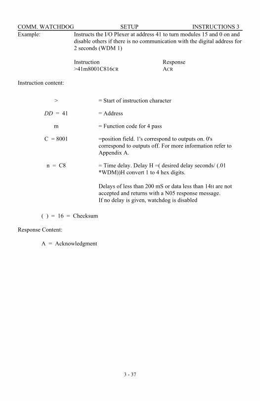
COMM. WATCHDOG SETUP INSTRUCTIONS 3
3 - 37
Example: Instructs the I/O Plexer at address 41 to turn modules 15 and 0 on anddisable others if there is no communication with the digital address for2 seconds (WDM 1)
Instruction Response>41m8001C816CR ACR
Instruction content:
> = Start of instruction character
DD = 41 = Address
m = Function code for 4 pass
C = 8001 =position field. 1's correspond to outputs on. 0'scorrespond to outputs off. For more information refer toAppendix A.
n = C8 = Time delay. Delay H =( desired delay seconds/ (.01*WDM))H convert 1 to 4 hex digits.
Delays of less than 200 mS or data less than 14H are notaccepted and returns with a N05 response message. If no delay is given, watchdog is disabled
( ) = 16 = Checksum
Response Content:
A = Acknowledgment

COMM. WATCHDOG SETUP INSTRUCTIONS 3
3 - 38
Setup D (Analog Watchdog)
Instruction ResponseD watchdog position/ Delay -Analog >MADcg( )CR ACR
Purpose: Setup D (Analog ) sets up the time delay and can set modules to zeroor full scale when a serial watchdog failure occurs. If used inconjunction with Setup m (analog), it can set up levels other than zeroand full scale when a serial watchdog occurs.
Address: Any master analog address
Caution: For g = 0-7 the table presented overrides any values previously setby setup m (analog).
Reference: For general information on communication watchdogs, refer to thewatchdog introduction section.
Example: Instructs the analog address 83 to output full scale to module 0 and 7if there is no activity on the analog address line for 10 seconds.
Instruction Response>83D00815ADCR ACR
Instruction content:
> = Start of instruction character
83 = Master Analog Address
D = Function Code
c = 0081 = Position field. 1's specify which modules are to beaffected. 0's are disregarded. For more information refer toappendix A

COMM. WATCHDOG SETUP INSTRUCTIONS 3
3 - 39
g = 5 Time / Action from the table below or inactive communication time.
Values for g can range from 0-7 or 14H-FFFFH
g Time Action
0 Disable
1 10 Seconds Write Zero scale
2 1 Minute Write Zero scale
3 10 Minutes Write Zero scale
4 Disable
5 10 Seconds Write full scale
6 1 Minute Write full scale
7 10 Minutes Write full scale
If setup m is used, setup D configures the time delay and setup m specifies the output levels.
Delay = (0.01 seconds * WDM)H Convert 1 to 4 hex digits.
Delays of less than 200 mSec 14H are not accepted and return a N07 responsemessage.
If no delay is given, the watchdog is disabled
If WDM is in effect, all of the above times are multiplied by 256.( ) = AD = Checksum
Response Content:
A = Acknowledgment

COMM. WATCHDOG SETUP INSTRUCTIONS 3
3 - 40
Setup m (Analog Watchdog)
Instruction Response
m Watchdog Position/ levels >MAmc. . . l( )CR ACR(Analog)
Purpose: Setup m must be used in conjunction with setup D (Analog). Setup D determines thedelay period and setup m determines the output levels the analog outputs go to whena serial communication watchdog failure occurs.
Address: Any master analog address.
Caution: All analog modules that are not given a specific level are set to zero scale.
If in setup D (analog) g = 0 - 7, then any previous levels set by setupm are ignored.
Reference: For general information on communication watchdogs, refer to thewatchdog introduction section.

COMM. WATCHDOG SETUP INSTRUCTIONS 3
3 - 41
Example: Instructs the I/O Plexer at address 81 to output the value 800H (1/2scale) to analog output module 12 and the value FFFH (Full scale) tomodule 7, if a serial watchdog timeout occurs.
Instruction Response
>81m1080800FFF09CR ACR
Instruction content:
> = Start of instruction character
MA = 81 = Address
m = Function code
c = 1080 = Position field. 1's specify which modules are to beaffected. 0's are disregarded. For more information referto appendix A.
l = 800FFF = Output value. 3 hex digits represent the level sent toeach module chosen in the position field. The values aresent out ordered from the highest (15) to lowest (0)
( ) = 09 = Checksum
Response Content:
A = Acknowledgment

COMM. WATCHDOG SETUP INSTRUCTIONS 3
3 - 42
Setup eD, dD (Watchdog)
Instruction ResponseeD Watchdog multiplier - Enable >MCeD( )CR ACRdD Watchdog multiplier - Disable >MCdD( )CR ACR
Purpose: This instruction allows the watchdog delay time to be multiplied by256. This extends the maximum watchdog delay time from 10.9minutes to 46.6 hours.
Prerequisite: None
Defaults: Watchdog multiplier = 1
Battery backed: The underlined instruction data is saved in memory if:
1) The I/O Plexer has the /M memory optionAND
2)Setup eF instruction is issued after the system is configured asdesired.
Address: Any master control address
Remarks: This affects all communication watchdogs both analog and digital.
When this instruction is enabled, WDM = 256

COMM. WATCHDOG SETUP INSTRUCTIONS 3
3 - 43
Example: This instruction enables the watchdog multiplier at all addressesconnected to this master control address. This means that any time a 1second delay is sent using setup D or m it is multiplied by 256 for anactual delay of 256 seconds.
Instruction Response
>00eD09CR ACR
Instruction content:
> = Start of instruction character
MC = 00 = Master Control Address
eD = Function code
( ) = 09 =checksum
Response Content:
A = Acknowledgment

TRM SETUP INSTRUCTIONS 3
3 - 44
Setup n
Instruction Response
n Set Timer Resolution Multiplier >DDny( )CR ACR
Purpose: Sets the resolution multiplier of the internal 10mSec clock whichaffects the timing of all of the digital instructions listed below.
Prerequisite: None
Default: TRM = 1. Timer resolution = 0.001 seconds.
Battery Backed: The underlined instruction data is saved in memory if:
1) The I/O Plexer has the /M memory option AND
2) Setup eF instruction is issued after the system is configured asdesired.
Address: Any master or digital expander 1 address.
Caution: There are separate multipliers for the master digital and the digitalexpander 1 address. Sending this instruction to one has no effect onthe other.
Do not confuse this with watchdog multiplier, WDM
Remarks: This instruction alters the period of the digital squarewave and otherinstructions listed below if changed during operation.

TRM SETUP INSTRUCTIONS 3
3 - 45
Instructions Affected by Setup nDigital h Retrigger time delayDigital K Start ON pulseDigital R Start Off pulseDigital d Read pulse complete bitsDigital e Read duration countersDigital f Read and clear Duration countersDigital Z. . H One Shot onDigital Z . .J One shot offDigital Z. . I Delayed onDigital Z. . K Delayed offDigital Z . .L Square WaveDigital Z . .M Fast square Wave
Example: This instruction sets the timer resolution to 150 mSec per count.
Instruction Response
>40n0F48 ACR
Instruction content:
> = Start of instruction character
DD = 40 = Digital Address
n = Function code
y = 0F =Timer Resolution. Resolution = Desired multiplierconverted to 2 hex digits. It can range from 0 to 255 (FFH)
( ) = 48 = Checksum
Response Content:
A = Acknowledgment

RESPONSE TAGS SETUP INSTRUCTIONS 3
3 - 46
Setup eA, dA
Instruction Response
eA Enable Address Tag >MCeA( )CR ACRdA Disable Address Tag >MCdA( )CR ACR
Purpose: Provides the means for appending an address to the I/O Plexerresponses.
Prerequisite: None
Defaults: Address tags disabled
Battery backed: The underlined instruction data is saved in memory if:
1) The I/O Plexer has the /M memory optionAND
2) Setup eF instruction is issued after the system is configured asdesired.
Address: Master control address only, but this is a global instruction. It affectsall addresses associated with this master control address such as themaster digital, master analog, and digital expander 1.

RESPONSE TAGS SETUP INSTRUCTIONS 3
3 - 47
Remarks: Setup eA instruction causes the responses to add the two characteraddress of the instruction to the end of the response. The addresscharacters are preceded and followed by *.
Example Enables the address tag.
Instruction Response
>00eA06CR ACR
Instruction content:
> = Start of instruction character
MC = 00 = Master Control Address
eA = Function code
( ) = 06 =checksum
Response Content:
A = Acknowledgment
Example: Disables address tag
Instruction Response
>00dA05CR A *00* CR

RESPONSE TAGS SETUP INSTRUCTIONS 3
3 - 48
Setup eC, dC
Instruction Response
eC Enable Checksum tag >MCeC( )CR ACRdC Disable Checksum tag >MCdC( )CR ACR
Purpose: Provides the means for appending correct checksum to the I/O Plexerresponses.
Prerequisite: None
Defaults: Checksum tag disabled
Battery Backed: The underlined instruction data is saved in memory if:
1) The I/O Plexer has the /M memory option AND
2) Setup eF instruction is issued after the system is configured asdesired.
Address: Master control address only, but this is a global instruction. It affectsall addresses associated with this master control address such as themaster digital, master analog, and the digital expander 1.

RESPONSE TAGS SETUP INSTRUCTIONS 3
3 - 49
Remarks: Setup eC instruction allows the user to specify any 2 character Hexvalue in the checksum position. The I/O Plexer returns an N02response message with the correct checksum framed in “ * “. WhenN02 is returned, the instruction is not executed. If no N02 checksumresponse is returned, then the checksum used was correct. “??” isprocessed as ignore checksum which defeats the purpose of usingchecksums.
Example: Enables the checksum tag
Instruction Response
>00eC08CR ACR
Instruction content:
> = Start of instruction character
MC = 00 = Master Control Address
eC = Function code
( ) = 08 =checksum
Response Content:
A = Acknowledgment
Example: Disables Checksum tag
Instruction Response
>00dC07CR A * ( ) *CR

ERROR MESSAGES SETUP INSTRUCTIONS 3
3 - 50
Setup eE, dE
Instruction Response
eE Enable Error messages >MCeE( )CR ACRdE Disable Error messages >MCdE( )CR ACR
Purpose: Provide the means for disabling the return of error messages that thehost software may not be able to handle.
Prerequisites: None
Default: Error message enabled
Battery Backed: The underlined instruction data is saved in memory if:
1) The I/O Plexer has the /M memory option AND
2) Setup eF instruction is issued after the system is configured asdesired.
Address: Master Control address only. but this is a global instruction. It affectsall addresses associated with this master control address such asmaster digital, master analog, and the digital expander 1.

ERROR MESSAGES SETUP INSTRUCTIONS 3
3 - 51
Caution: There is NO response when an error occurs. This condition may causethe host to wait indefinitely for a response that will never be issued.
Example: Disables error messages
Instruction Response
>00dE009CR ACR
Instruction content:
> = Start of instruction character
MC = 00 = Master Control Address
dE = Function code
( ) = 09 =checksum
Response Content:
A = Acknowledgment

BATTERY BACKED SETUP INSTRUCTIONS 3
3 - 52
Setup eF, dF
Instruction Response
eF Save Setup >MCeF( )CR ACRdF Disable Setup >MCdF( )CR ACR
Purpose: Allows the configuration information to be saved in battery backedRAM, while power is off. Must have /M option.
Prerequisite: None
Default: Disable
Battery Backed: The underlined instruction data is saved in memory if:
1) The I/O Plexer has the /M memory optionAND
2) The eF instruction is issued after the system is configured asdesired.
Address: Master Control address only, but this is a global instruction. It affectsall addresses associated with this master control address such as themaster digital, master analog, and the digital expander 1.
Remarks: When setup eF instruction is sent, the I/O Plexer calculates and storesa checksum of the configuration data. During power up a newchecksum is computed. If it agrees with the stored one, the system isconfigured as it was before the power cycle. If they do not agree, thesystem is initialized to the default state as if there was no batterybackup.

BATTERY BACKED SETUP INSTRUCTIONS 3
3 - 53
Caution: Changing the configuration after issuing setup eF changes thechecksum. After all changes, setup eF must be re-issued to save theconfiguration.
Example This instruction saves the system configuration as it is at the time it was sent.
Instruction Response
>00eF0BCR ACR
Instruction content:
> = Start of instruction character
MC = 00 = Master Control Address
eF = Function code
( ) = 0B =checksum
Response Content:
A = Acknowledgment

ADDRESSING SETUP INSTRUCTIONS 3
3 - 54
Setup a, b
a set Variable Address
Instruction Response
>MCaMCMDMAEIMF( )CR AMCMDMAEIMF( )CR
b Read Variable Address
>MCb( )CR AMCMDMAEIMF( )CR
Purpose: Provides a way to set up variable addressing in an I/O Plexer orprovides a way to check the addressing of a particular I/O Plexer.
Prerequisite: None
Remarks: MC =Master addressMD =Master Digital addressMA =Master Analog addressE1 =digital Expander 1 addressMF =Master Future address

ADDRESSING SETUP INSTRUCTIONS 3
3 - 55
Default: Offset addressing automatically sets the addresses based on the MasterControl address. It is shown below.
Master digital address =40H+ Master Control address
Master analog address =80H+ Master Control Address (defaults to MC if notpresent)
Digital Expander 1 address =C0H + Master Control address (defaults to MC if notpresent)
Master Future = Master Control address
Offset addressing allows setting the master control address to any value from 00H to3FH. Using setup a allows any address to be set to any value from 00H to FFH.

ADDRESSING SETUP INSTRUCTIONS 3
3 - 56
Caution: This instruction can also reset the Master control address. Oncechanged, the new Master control address is required to change it back.Powering down will not bring it back in its previous state.
Battery Backed: No effect, always saved
Address: Any master control address
Example: This requests the addresses associated with master control. 00H
Instruction Response>00bC2CR A004080C000FFCR
Instruction content:
> = Start of instruction character
MC = 00 = Master Control Address
a = Function code
( ) = C1 =checksum
Response Content:
A = AcknowledgmentMC = 00 New master control addressMD = 40 New Master Digital addressMA = 80 New master analog addressE1 = C0 New digital expander 1 addressMF = 00 Master Future address( ) = FF Checksum

ADDRESSING SETUP INSTRUCTIONS 3
3 - 57
Example 2: This instruction changes the addresses associated with master control address 00H
Instruction Response>00a0506070805C0CR A0506070805FFCR
Instruction Content:
> - start of instruction character
MC = 00 - Master control address
a - function code
MC = 05 - Master control address
MD = 06 - Master digital address
MA = 07 - Master analog address
E1 = 08 - Digital expander 1 address
MF = 05 - Master future address
( ) = CO - Checksum
Response Content:
A - Acknowledgment
MC = 05 - Master control address
MD = 06 - Master digital address
MA = 07 - Master analog address
E1 = 08 - Digital expander 1 address
MF = 05 - Master future address
( ) = FF - Checksum

NOTES INSTRUCTIONS 3
3 - 58

DIGITAL INPUTS INSTRUCTIONS 3
3 - 59
Page
Introduction 3-60
Status 3-62
M read all modules
Pulse Duration 3-64
a Set all trigger edges
b Set positive trigger edges
c Set negative trigger edges
d Measurements Complete
e Read duration complete
g Clear duration counters
f Read and Clear counters
y Pulse accumulator -enable
z Pulse accumulator -disable
Pulse Counting 3-72
W read Counters
X Read and Clear counters
Y Clear Counters
U Start Counters
V Stop Counters
T Start/ Stop Counters
Edge Detection 3-76
N set all latch edges
O Set latches Off to On
P Set latches On to Off
Q Read latches
S Clear Latches
R Read and Clear Latches

INTRODUCTION DIGITAL INPUTS INSTRUCTIONS 3
3 - 60
DIGITAL INPUT INTRODUCTION
PICTORIAL GLOSSARY
Digital a, b, c
Digital e,f
Time n is collected. Only the first pulse is measured. It must be reset to measure anotherpulse.

INTRODUCTION DIGITAL INPUTS INSTRUCTIONS 3
3 - 61
Digital y
Pulse duration measurement with Accumulator option and positive edgetriggering produces the followingresults:
nT = n1 + n2 + n3
nT = Total On time accumulated over all pulses
Digital W, X, Y, U, V, T
Pulse counter counts the number of pulses
Digital N, O, P, Q, R, S

STATUS DIGITAL INPUTS INSTRUCTIONS 3
3 - 62
Digital M
Instruction ResponseM Read all modules >DDM( )CR AcCR
Purpose: Determines the on/ off state of all digital I/O positions, both input andoutput.
Prerequisite: Configure as inputs using step G or H
Default: None
Battery Backed: Not applicable
Address: Any master digital or digital expander 1 address.
Caution: The instruction does NOT read the physical output at the terminalstrip, but the actual value last sent by the I/O Plexer.

STATUS DIGITAL INPUTS INSTRUCTIONS 3
3 - 63
Example: This instruction reads the status of all digital modules. The responseindicates that the module 4 and 5 are on.
Instruction Response>40MB1CR A0030C3CR
Instruction Content:
> - start of instruction character
DD = 40 - Digital address
M - function code
( ) = B1 - Checksum
Response Content:
A - Acknowledgment
c = 0030 - Position Field, 1's mean the module is on, 0'smean they are off. The modules can be inputs oroutputs. For more information refer to appendixA
( ) = C3 - Checksum

PULSE DURATION DIGITAL INPUTS INSTRUCTIONS 3
3 - 64
Digital a, b, c
Instruction Response
a Set All triggers edges >DDae( )CR ACRb Set Positive trigger edges >DDbe( )CR ACRc Set Negative trigger edges >DDce( )CR ACR
Purpose: Set triggers edges for pulse duration measurements. Digital a can beused if all inputs are to have a duration measurement, otherwiseDigital b and c should be used.
Prerequisites: These instructions should be used before duration counter instructions,digital d, e, and f
Default: Negative trigger edges
Battery Backed: The underlined instruction data is saved in memory if:
1) The I/O Plexer has the /M memory optionAND
2) Setup eF instruction has been issued after the system is configuredas desired.
Address: Any master digital or digital expander 1 address
Remarks: Positive trigger edge is for off on off pulse. Negative trigger edge isfor on off on pulses.

PULSE DURATION DIGITAL INPUTS INSTRUCTIONS 3
3 - 65
Example: Modules 4 and 5 are set to measure positive trigger edges.
Instruction Response>40b003089CR ACR
Instruction content:
> = Start of instruction character
DD = 40 = Digital Address
b = Function code
e = 0030 = Position field
Digital a 1's set positive trigger edges
0's set negative trigger edges
Digital b 1's set positive trigger edges
0's are disregarded
Digital c 1's are negative trigger edges
0's are disregarded
If this field is omitted, FFFFH is assumed by the I/O Plexer. Leadinghex zeroes may be omitted. For more information , refer to appendixA.
( ) = 89 = Checksum
Response content:
A = Acknowledgment

PULSE DURATION DIGITAL INPUTS INSTRUCTIONS 3
3 - 66
Digital d
Instruction Response
d Measurement complete >DDd( )CR Ac( )CR
Purpose: Determines which positions have completed full pulse durationmeasurement.
Prerequisites: Set the duration trigger edges using the digital a, b, or c instruction.Initialize duration counters to zero with the digital f or g instruction.
Default: Configure as inputs using setup G or H
Battery backed: Not applicable
Address: Any master digital or digital expander 1 address.
Remarks: A measurement complete bit is set to indicate entire pulse has beengathered. The host can read this bit to see if measurements arecomplete and then read the duration counters. No other durations willbe measured until complete bit is cleared.
If the pulse duration is read (Digital e and f) before the pulse hadfinished, the partial duration is returned.
The measurement complete bit is cleared whenever digital f or g isissued, to clear pulse duration.

PULSE DURATION DIGITAL INPUTS INSTRUCTIONS 3
3 - 67
Caution: These instructions are affected by the setup n instruction, which canadjust the timer resolution multiplier, TRM.
If pulse accumulator, digital y, is used the measurement complete setbit is never set.
Example: This instruction asks which modules have completed a pulse durationmeasurement. The response indicates that module 4 has completed it.
Instruction Response
>40dC8CR A0010C1CR
Instruction content:
> = Start of instruction character
DD = 40 = Digital Address
d = Function code
( ) = C8 = checksum
Response Content:
A = Acknowledgment
C = 0010 = Position field. The 1's bits have completed theirspecified off on off, or on off on sequence. 0's have notcompleted transition or are not digital inputs
( ) = C1 =checksum
PULSE DURATION DIGITAL INPUTS INSTRUCTIONS 3
3 - 68
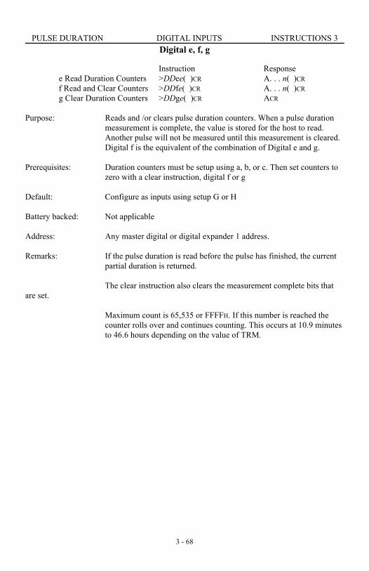
Digital e, f, g
Instruction Responsee Read Duration Counters >DDee( )CR A. . . n( )CRf Read and Clear Counters >DDfe( )CR A. . . n( )CRg Clear Duration Counters >DDge( )CR ACR
Purpose: Reads and /or clears pulse duration counters. When a pulse durationmeasurement is complete, the value is stored for the host to read.Another pulse will not be measured until this measurement is cleared.Digital f is the equivalent of the combination of Digital e and g.
Prerequisites: Duration counters must be setup using a, b, or c. Then set counters tozero with a clear instruction, digital f or g
Default: Configure as inputs using setup G or H
Battery backed: Not applicable
Address: Any master digital or digital expander 1 address.
Remarks: If the pulse duration is read before the pulse has finished, the currentpartial duration is returned.
The clear instruction also clears the measurement complete bits thatare set.
Maximum count is 65,535 or FFFFH. If this number is reached thecounter rolls over and continues counting. This occurs at 10.9 minutesto 46.6 hours depending on the value of TRM.

PULSE DURATION DIGITAL INPUTS INSTRUCTIONS 3
3 - 69
Caution: If pulse accumulation is being used (digital y) accumulated durationsare read. Otherwise only the first pulse is measured. These instructionsare affected by the setup n instruction which can adjust the timerresolution multiplier (TRM)
Example: This instruction requests the duration for modules 4 and 5. Module 5has a duration of 3.23 seconds and module 4 has a duration of 2.4seconds assuming TRM =1.
Instruction Response >40f00308DCR A014300f09ECR
Instruction content:
> = Start of instruction character
DD = 40 =Digital Address
f = Function code
e = 0030 =Position field. 1's select which modules duration to readand/ or clear. 0's are disregarded. If this field is omitted,FFFFH is assumed by the I/O Plexer. Leading hex zeroesmay be omitted. For more information refer to appendixA.
( ) = 8D = Checksum
Response Content:
A = Acknowledgment
n = 014300F0 = Pulse duration. 4 hex are returned for each moduleselected in the instruction’s position field. Values arereturned from the highest module (15) to lowest module(0). ???? are returned if the module is not a digital input.
Duration(Seconds)
Decimal value of n * TRM * 0.01 Seconds
Module 4 00F0H * TRM * 0.01 sec = 2.4 Sec * TRM
Module 5 0143H * TRM* 0.01sec = 3.23 * TRM
( ) = 9E Checksum

PULSE DURATION DIGITAL INPUTS INSTRUCTIONS 3
3 - 70
Digital y, z
Instruction Response
y Pulse Accumulator -enable >DDye( )CR ACRz Pulse Accumulator - Disable >DDze( )CR ACR
Purpose: This instruction is related to the instruction set of Digital a throughDigital g. It allows the duration counter to accumulate the total pulsewidth of a train of pulses rather than just one pulse.
Prerequisite: Digital a, b, or c must be used to set up the trigger edges. Digital e, f,and/ or g may be used to read and or clear the duration.
Default: Disabled
Battery Backed: The underlined instruction data is saved in memory if:
1) The I/O Plexer has the /M memory optionAND
2) Setup eF instruction is issued after the system is configured asdesired.
Address: Any master digital or digital expander 1 address.
Caution: Pulse complete bits (Read with digital d) are never set for positionsmodified by Digital y.

PULSE DURATION DIGITAL INPUTS INSTRUCTIONS 3
3 - 71
Example: This instruction enables pulse accumulation at module 8 and 5.
Instruction Response
>40y0120A0CR ACR
Instruction content:
> = Start of instruction character
DD = 40 = Digital Address
y = Function code
e = 0120 = Position field. 1's select which modules are effected, 0'sare disregarded. If this field is omitted FFFFH is assumedby the I/O Plexer. Leading hex zeroes may be omitted. Formore information see appendix A
( ) = A0 = Checksum
Response Content:
A = Acknowledgment

PULSE COUNTING DIGITAL INPUTS INSTRUCTIONS 3
3 - 72
Digital U, V, T
Instruction Response
U Start Counters DDUe( )CR ACRV Stop counters DDVe( )CR ACRT Start/ stop computers DDTe( )CR ACR
Purpose: To stop and or start digital counters
Prerequisites: Digital Y or X should be used to clear the counters before usingDigital U or T to start counting.
Default: Active
Battery Backed: Not applicable
Address: Any master digital or digital expander 1 address
Remarks: Pulse rates up to 400 counts / sec with minimum on and off pulsewidth of 1.0millisecond can be counted. Counts off to on transitions.
Caution: Digital T instruction stops all counters that are specified as zeroes inthe position field.

PULSE COUNTING DIGITAL INPUTS INSTRUCTIONS 3
3 - 73
Example: This instruction starts counters for modules 4 and 5 and stops all othercounters.
Installation Response
>40T00307BCR ACR
Instruction content:
> = Start of instruction character
DD = 40 = Digital Address
T = Function code
e = 0030 = Position field.
Digital U : 1's start counters 0's are disregarded
Digital V : 1's stop the counters0's are disregarded
Digital T : 1's start the counters0's stop the counters
( ) = 7B = Checksum
Response Content:
A = Acknowledgment

PULSE COUNTING DIGITAL INPUTS INSTRUCTIONS 3
3 - 74
Digital W, Y, X
Instruction Response
W Read Counters >DDWe( )CR A. . . n( )CRY Clear Counters >DDYe( )CR ACRX Read & Clear Counters >DDXe( )CR A. . . n( )CR
Purpose: Reads and/ or resets the counters to zero. Digital X is equivalent tosending the digital W followed by Digital Y.
Prerequisite: Before the counters are read using digital W or X they should bestarted using Digital U or T and set to zero using digital Y and X.
Default: Not applicable
Battery Backed: Not applicable
Address: Any master digital or digital expander 1 address
Remarks: Only clear instructions, Digital Y and X, reset counters.
Pulse rates of up to 400 counts/ second with a minimum on and offpulse width of 1.0 millisecond can be counted.
If the count exceeds the maximum count of 65,535 = FFFFH it rollsover to zero and continues counting.

PULSE COUNTING DIGITAL INPUTS INSTRUCTIONS 3
3 - 75
Example: This instruction returns the counts for module positions 4 and 5, thenclears the counters. The response indicates that module 5 had 4 pulsesand module 4 had 10 pulses since the last start / clear instruction.
Instruction Response>40X00307FCR A0004000A95CR
Instruction content:
> = Start of instruction character
DD = 40 = Digital Address
X = Function code
e = 0030 = Position field. 1's select which modules are read, 0's aredisregarded. If this field is omitted, FFFFH is assumed bythe I/O Plexer. Leading Hex zeroes may be omitted. Formore information see appendix A
( ) = 7F = Checksum
Response content:
A = Acknowledgment
n = 0004000A = Pulse counts. Each module specified in the instructionreturns a 4 digit hex count. Convert this to decimal foractual count. Counter values are returned in sequencefrom highest to lowest (15 -0). ???? is returned if theselected module was not a digital input.
Module 4 = 004H = 4 countsModule 5 = 000AH = 10 counts
( ) = 95 = Checksum

EDGE DETECTION DIGITAL INPUTS INSTRUCTIONS 3
3 - 76
Digital N, O, P
Instruction Response
N Set All Latch Edges >DDNe( )CR ACRO Set Latches Off to On >DDOe( )CR ACRP Set Latches On to Off >DDPe( )CR ACR
Purpose: Sets up latch edges for On to Off or Off to On transitions. The DigitalN instruction affects all input positions.
Prerequisites: Configure as inputs using Setup G or H.
Default: Latch Off to On transitions.
Battery Backed: The underlined instruction data is saved in memory if:
1) The I/O Plexer has the /M memory optionAND
2) Setup eF instruction is issued after the system is configured asdesired.
Address: Any master digital or digital expander 1 address.
Remarks: Latches are set only when the specified transition occurs. Once a latchis set it will not change until a clear instruction Digital S or R resetsthe transition detecting latch.

EDGE DETECTION DIGITAL INPUTS INSTRUCTIONS 3
3 - 77
Example: This instruction sets modules 4 and 5 to latch On to Off. The rest ofthe modules latch Off to On.
Instruction Response
>40N003075CR ACR
Instruction content:
> = Start of instruction character
DD = 40 = Digital Address
N = Function code
e = 0030 = Position field.Digital N : 1's latch on to off
0's latch off to onDigital O : 1's latch off to on
0's are disregardedDigital P : 1's latch on to off
0's are disregarded If this field is omitted FFFFH is assumed bythe I/O Plexer. Leading hex zeroes may beomitted. For more information see appendixA
( ) = 75 = Checksum
Response content:
A = Acknowledgment

EDGE DETECTION DIGITAL INPUTS INSTRUCTIONS 3
3 - 78
Digital Q, R, S
Instruction Response
Q Read Latches >DDQ( )CR AcCRR Read and Clear Latches >DDRe( )CR AcCRS Clear Latches >DDSe( )CR ACR
Purpose: Reads and / or Clears latches that have been set. Digital Q and R readsALL latches, regardless of the position field. Only the latches in thespecified positions are cleared.
Prerequisites: Latch direction must be set using Digital N, O, P and cleared usingDigital S or R, before they can be read.
Default: Not applicable
Battery Backed: Not applicable
Address: Any master digital or digital expander 1 address
Remarks: Latches are set only when the specified transition occurs. Only cleartype instructions Digital R or S Reset transition detecting latches.
Latches can detect pulses that are 1 mSec (0.001 seconds) or longer.

EDGE DETECTION DIGITAL INPUTS INSTRUCTIONS 3
3 - 79
Example: Instruction reads all the latches on the I/O Plexer at address 40 andclears latches if they are set for modules 4 and 5. The responseindicates module 4 and 12 have latched and that module 4 wascleared.
Instruction Response
>40R003079CR A1010C2CR
Instruction content:
> = Start of instruction character
DD = 40 = Digital Address
R = Function code
c = 0030 = Position field. 1's select which modules latches clear, 0'sare disregarded. If this field is omitted FFFFH is assumedby the I/O Plexer. Leading hex zeroes may be omitted. Formore information see appendix A
( ) = 79 = Checksum
Response content:
A = Acknowledgment
c = 1010 = Position field. 1's mean the latch has been set. 0's meanthe latch hasn’t been set. For more information refer toappendix A
y = Function code
( ) = C2 = Checksum

NOTES INSTRUCTIONS 3
3 - 80

DIGITAL OUTPUTS INSTRUCTIONS 3
3 - 81
Page
Introduction 3-82
Status 3-84
M Read all Modules
J Set all Modules Off 3-86
K Set On
L Set Off
Modifiers 3-88
Z..G Disable waveform
Z..H One Shot On
Z..J One Shot Off
Z..I Delay On
Z..K Delay Off
Z..L Squarewave
Z..M Fast Squarewave
h Retrigger time delay
Pulses 3-98
i Generate n pulses
k start On pulse
l start Off pulse

INTRODUCTION DIGITAL OUTPUTS INSTRUCTIONS 3
3 - 82
DIGITAL OUTPUT INTRODUCTION
PICTORIAL GLOSSARY
Digital Z. . .H and Z. . .JOne Shot ON/ OFF instructions
Digital Z. . I and Z. . KDelayed ON/ OFF instructions

INTRODUCTION DIGITAL OUTPUTS INSTRUCTIONS 3
3 - 83
Digital Z . . L and Z . . MSquarewave and Fast squarewave
Digital iGenerate n Pulses
1 2 3

STATUS DIGITAL OUTPUTS INSTRUCTIONS 3
3 - 84
Digital M
Instruction Response
M Read all Modules >DDM ( )CR AcCR
Purpose: Reads the On/ Off state of all digital I/O positions, inputs and outputs.
Prerequisite: None
Default: None
Battery Backed: Not applicable
Address: Any master digital or digital expander 1 address
Caution: This instruction does not read the physical output at the terminal strip,but actually the last value sent from the I/O Plexer.

STATUS DIGITAL OUTPUTS INSTRUCTIONS 3
3 - 85
Example: This instruction reads the current value of all digital modules. Theresponse indicates that module 4 and 5 are On and the rest of themodules are Off OR not digital
Instruction Response
>40MB1CR A0030C3CR
Instruction content:
> = Start of instruction character
DD = 40 = Digital Address
M = Function code
( ) = B1 = Checksum
Response content:
A = Acknowledgment
c = 0030 = Position Field. 1's mean the module is on, 0's mean themodule is off. The module can be input or output. Formore information refer to appendix A
( ) = C3 = Checksum

STATUS DIGITAL OUTPUTS INSTRUCTIONS 3
3 - 86
Digital J, K, L
Instruction Response
J Outputs On/ Off >DDJe( )CR ACRK Outputs On >DDKe( )CR ACRL Outputs Off >DDLe ( )CR ACR
Purpose: Turns specified outputs On or Off. Digital J should be used only if alldigital modules at this address are to be set, otherwise use Digital Kand L.
Prerequisite: Configure module positions as either inputs or outputs using Setup Gor I
Default: Output modules Off
Battery Backed: Not applicable
Address: Any master digital or digital expander 1 address
Caution: If modifiers (digital Z instructions) are set up, outputs are affectedaccordingly when Digital J, K or L is sent.

STATUS DIGITAL OUTPUTS INSTRUCTIONS 3
3 - 87
Example: Turn On modules 0-7, and turn Off module8-15. Digital inputandanalog modules are not affected.
Instruction Response
>40J00FF9ACR ACR
Instruction content:
> = Start of instruction character
DD = 40 = Digital Address
J = Function code
c = 00FF = Position field.Digital J : 1's turn the module On0's turn the module OffDigital K : 1's turn the module On0's are disregardedDigital L : 1's turn the module Off0's are disregarded If this field is omitted FFFFH is assumed by the I/OPlexer. Leading hex zeroes may be omitted. For moreinformation see appendix A
( ) = 9A = Checksum
Response Content:
A = Acknowledgment

MODIFIERS DIGITAL OUTPUTS INSTRUCTIONS 3
3 - 88
Digital Z
Instruction ResponseDigital Z ModifiersOne Shot On >DDZeHn( )CR ACROne Shot Off >DDZeJn( )CR ACRTerminate >DDZeG( )CR ACR
Purpose: Produces an output that when turned On/Off stays in that state for thespecified time period and then returns to its initial state.When the one shot is no longer wanted it can be terminated usingdigital Z. . G
Prerequisite: Configure module positions as output using Setup G or I instruction.
Defaults: Modifiers disabled
Battery Backed: The underlined instruction data is saved in memory if :
1) The I/O Plexer has the /M memory protect optionAND
2) Setup eF is issued after the system is configured as desired.
Address: Any master digital or digital expander 1 address.
Caution: These instructions are affected by setup n, which adjusts the timerresolution multiplier, TRM. If a module is set for a one shot on, it hasno affect turning it off.

MODIFIERS DIGITAL OUTPUTS INSTRUCTIONS 3
3 - 89
The time delay is restarted when Digital J, K, or L resend the datawhich started the delay. Digital h does the same thing. Theseinstructions are ONLY modifiers and do not turn any modules On orOff. It performs its function only after Digital J, K, or L is sent.Terminating the instruction (Digital Z . .G) returns the output tonormal behavior and turns the module Off.
Example: This instruction directs the I/O Plexer at address40 to set module 2 forone shot On (off ON off). transition. The period for the On time is00C8H or 2 seconds if TRM = 1.
Instruction Response>40Z0004H00C8A5CR ACR
Instruction content:
> = Start of instruction character
DD = 40 = Digital Address
Z = Function code
e = 0004 = Position field. 1's select which modules are effected, 0'sare disregarded. This field must consist of at least onedigit . Leading hex zeroes may be omitted. For moreinformation see appendix A
H =Function Code for specifying modifier type
n = 00C8 Time the signal is On/ Off
Time H (Desired time in seconds/ (.01 seconds *TRM))Convert 1-4 Hex digits,Special Case:n = 0H is equivalent to 65,536 (approximately 10.9Minutes assuming TRM = 1)
( ) = 5 = Checksum
Response Content:
A = Acknowledgment

MODIFIERS DIGITAL OUTPUTS INSTRUCTIONS 3
3 - 90
Digital Z (Continued)
Instruction Response
Digital Z ModifiersDelayed On >DDZeln( )CR ACRDelayed Off >DDZeKn( )CR ACRTerminate >DDZeG( )CR ACR
Purpose: Puts in a time delay before the module is turned Off or On. If thedelay is no longer desired it can be terminated by Digital Z. . . G
Prerequisite: Configure as output using setup G or I instruction.
Defaults: Modifiers Disabled
Battery Backed: The underlined instruction data is saved in memory if :
1) The I/O Plexer has the /M memory protect optionAND
2) Setup eF is issued after the system is configured as desired.
Address: Any master digital or digital expander 1 address.
Caution: These instructions car affected by setup n, which adjusts the timerresolution multiplier, TRM. The time delay starts over wheneverdigital h is sent or Digital J, K, or L. If a module is setup for delay On,there is no delay in turning it Off.

MODIFIERS DIGITAL OUTPUTS INSTRUCTIONS 3
3 - 91
These instructions are ONLY modifiers and do not turn any moduleson/ off.It performs its function only after digital J, K, or L is sent.Terminating the instruction (Digital Z. . .G) return the output tonormal behavior and turns the module off.
Example This instruction sets up module 0 to have a delayed On of 2 secondsassuming TRM=1
Instruction Response
>40Z0001I00C8A3CR ACR
Instruction content:
> = Start of instruction character
DD = 40 = Digital Address
Z = Function code
e = 0001 = Position field. 1's select which modules are effected, 0'sare disregarded. This field must consist of at least onedigit . Leading hex zeroes may be omitted. For moreinformation see appendix A
I =Function Code for specifying modifier type
n = 00C8 Time the signal is On/ Off
Time H (Desired time in seconds/ (.01 seconds *TRM))Convert To 4 Hex digits,Special Case:n = 0H is equivalent to 65,536 (approximately 10.9Minutes assuming TRM = 1)
( ) = 5 = Checksum
Response Content:
A = Acknowledgment

MODIFIERS DIGITAL OUTPUTS INSTRUCTIONS 3
3 - 92
Digital Z (Continued)
Instruction Response
Digital Z ModifiersSquarewave >DDZeLtu( )CR ACRTerminate >DDZeG( )CR ACR
Purpose: Digital Z . .L generates waves with periods from 0.02 t21.8 minutes.Digital Z. . M Generates waves with periods from 5.12 to 92.8 hours.
Prerequisite: Configure module position as output using Setup G or I instruction.
Defaults: Modifiers disabled
Battery Backed: Not applicable
Address: Any master digital or digital expander 1
Remarks: Analog squarewave can be generated using analog R or V instruction.
Caution When the squarewave is terminated it goes to the off state.
Unlike other digital Z modifiers, squarewaves start immediately.

MODIFIERS DIGITAL OUTPUTS INSTRUCTIONS 3
3 - 93
Example: This instruction outputs a squarewave to module 2. The output is Offfor 4.26 minutes and on for 8.19 minutes.
Instruction Response
>40Z0004LC064ABCR ACR
Instruction content:
> = Start of instruction character
DD = 40 = Digital Address
Z = Function code
e = 0004 = Position field. 1's select which modules are effected, 0'sare disregarded. This field must consist of at least onedigit . Leading hex zeroes may be omitted. For moreinformation see appendix A
L =Function Code for specifying modifier type
t = C0 =Time the signal is On
u = 64 = off time Time H =(Desired time in seconds/ 2.56 Convert 2 Hexdigits,Special Case:t or u = 0H is equivalent to 65,536 (approximately 10.9Minutes assuming TRM = 1)
( ) = 5 = Checksum
Response Content:
A = Acknowledgment

MODIFIERS DIGITAL OUTPUTS INSTRUCTIONS 3
3 - 94
Digital Z (Continued)
Instruction Response
Digital Z ModifiersFast Squarewave >DDZeMtu( )CR ACRTerminate >DDZeG( )CR ACR
Purpose: Digital Z. . L generates waves with periods from 0.02 seconds to 21.8minutes. Digital Z. . M generates waves with periods from 5.12seconds to 92.8hours.
Prerequisite: Configure module position as output using G or I instruction.
Defaults: Modifiers disabled
Battery Backed: Not applicable
Address: Any master digital or digital expander 1 address
Remarks: Analog squarewaves can be generated by using Analog R or Vinstructions.
Unlike other digital Z modifiers, squarewaves start immediately.
Caution: When the squarewave is terminated it goes to the off state

MODIFIERS DIGITAL OUTPUTS INSTRUCTIONS 3
3 - 95
Example: This instruction inputs a squarewave to module 2. The output is turnedoff for 1.32 seconds and on for 1.0 second assuming TRM = 1
Instruction Response
>40Z004M6484A5CR ACR
Instruction content:
> = Start of instruction character
DD = 40 = Digital Address
Z = Function code
e = 0004 = Position field. 1's select which modules are effected, 0'sare disregarded. This field must consist of at least onedigit . Leading hex zeroes may be omitted. For moreinformation see appendix A
M =Function Code for specifying modifier type
t = 64 =Time the signal is On
u = 84 = off time Time H =(Desired time in seconds/ 2.56 Convert 2 Hexdigits,Special Case:t or u = 0H is equivalent to 65,536 (approximately 10.9Minutes assuming TRM = 1)
( ) = A3 = Checksum
Response Content:A = Acknowledgment

MODIFIERS DIGITAL OUTPUTS INSTRUCTIONS 3
3 - 96
Digital h
Instruction Response
h Re-trigger Time Delay >DDhe( )CR ACR
Purpose: This instruction restarts the time delay On Digital Z instructions. Thiscan also be accomplished by sending the module the same on/ off dataas that which started the delay.
Prerequisite: Configure module positions as output using G or I instruction
Defaults: None
Battery Backed: Not applicable
Address: Master digital or digital expander 1 address
Caution: This instruction affects delays set up by:
Z. . H One shot On Digital modifier instructionZ. . J One shot Off Digital modifier instructionZ. . I Delay On digital modifier instructionZ. . K Delay off digital modifier instruction
Note: this instruction does not affect squarewave generation.

MODIFIERS DIGITAL OUTPUTS INSTRUCTIONS 3
3 - 97
Example: Instruction re-triggers the time delay on module 3 and 6.
Instruction Response>40h004898CR ACR
Instruction content:
> = Start of instruction character
DD = 40 = Digital Address
H = Function code
e = 0048 = Position field. 1's select which modules are effected, 0'sare disregarded .If this field is omitted the I/O Plexerassumes the value FFFFH . Leading hex zeroes may beomitted. For more information see appendix A
( ) = 98 = Checksum
Response Content:
A = Acknowledgment

PULSES DIGITAL OUTPUTS INSTRUCTIONS 3
3 - 98
Digital i
Instruction Response
i Pulse 50% duty cycle >DDictn( )CR ACR
Purpose: Output a pulse train consisting of a specified number of pulses whichare on and off for equal amounts of time.
Prerequisite: Configure module position as digital outputs using the setup G or Iinstruction.
Default: None
Battery Backed: Not Applicable
Address: Any master digital or digital expander 1 address
Caution: These instructions are effected by the setup n instruction, whichadjusts the timer resolution multiplier, TRM.

PULSES DIGITAL OUTPUTS INSTRUCTIONS 3
3 - 99
Example: This instruction outputs a pulse train of 4 pulses whose On/ Off time is.5 seconds to module 13 and 0 assuming a TRM = 1
Instruction Response
>40i2001320004B9CR ACR
Instruction content:
> = Start of instruction character
DD = 40 = Digital Address
i = Function code
c = 2001 = Position field. 1's select which modules are effected, 0'sare disregarded. For more information see appendix A
t = 32 =Half period, The time shown is 50% duty cycle time orthe on time or the off time. On time = off time = halfperiod.tH=((Period in seconds)/(.01 Seconds * TRM))Convert to two hex digits
n = 004 =Number of pulses to be sent, 0-65535 or FFFFH are legalvalues.Special cases:n = FFFFH is treated as infiniten = 0H is treated as FFFFH
( ) = B9 = Checksum
Response Content:
A = Acknowledgment

PULSES DIGITAL OUTPUTS INSTRUCTIONS 3
3 - 100
Digital k, l
Instruction Response
k Start pulse On >DDkcn( )CR ACRR Start pulse Off >DD Rcn( )CR ACR
Purpose: Turns specified modules On or Off for a specified period of time.
Prerequisite: Configure as digital outputs using Setup G or I instruction.
Default: None
Battery Backed: Not applicable
Address: Any master digital or digital expander address
Caution These instructions are affected by the setup n, which adjusts the timerresolution TRM.
Remark: These instructions care similar to one shot waveforms Digital Z. . Hand Z. . J, except this actually performs the instruction when it is sent.Furthermore, they do not modify the behavior of the normal digital J,K, and L. Digital Z is a modifier which performs its task only whenthe module is turned On/ Off.
Once started, a pulse may be terminated early by issuing a digitaloutput instruction (Digital J, K, L, i, k, l) Do not use retrigger timedelay, Digital h with Digital k ir l.

PULSES DIGITAL OUTPUTS INSTRUCTIONS 3
3 - 101
Example: This instruction turns module 13 and 5 On a for period equivalent to01F4H or 5 seconds assuming TRM = M.
Instruction Response
>40k202001F46ECR ACR
Instruction content:
> = Start of instruction character
DD = 40 = Digital Address
c = 2020 = Position field. 1's select which modules are effected, 0'sare disregarded. For more information see appendix A
n = 01F4 =Time module is on/ off. nH = ((Time desired in seconds)/ (.01 seconds * TRM))Convert to 1 to 4 hex digits.Special cases:n = 0 does nothing
( ) = 6E = Checksum
Response Content:
A = Acknowledgment

NOTES INSTRUCTIONS 3
3 - 102

ANALOG INPUTS INSTRUCTIONS 3
3 - 103
PageIntroduction 3-104Input Value 3-108L Read
Offsets 3-110g Calculate offseth Calculate & Set offsetsW Set offsets
Gains (Slopes) 3-114X calculate gainsZ calculate gainsY calculate gains
Range Limits 3-118N set rangesO read range errorsQ Clear range errorsP read and clear errors
Minimum/ Maximum Values 3-122a read lowest valueb clear lowest valuec read and clear lowest valued read highest valuee clear highest valuef read and clear highest
Averages 3-124M read and averageT start averagingi averaging completeU read averaged inputs
Temperature 3-130k Set temperature sensorR Read temperature inputs

INTRODUCTION ANALOG INPUTS INSTRUCTIONS 3
3 - 104
ANALOG INPUT INTRODUCTION
Analog input modules range is divided into 4095 segments - 12 Bit resolution. The values arerepresented by 4 hex digits. The first hex digit is the “range” digit. If it is a 1, the reading is inrange. The I/O Plexer handles values from 0F00H to 2BFFH. The module its self may not beable to generate values to the high and low end of this scale. There is NO guarantee ofaccuracy for values outside of 1000H to 1FFFH range If the module reads a value that isoutside of the range it will report 000H or 3000H depending if its over or under scale. If ananalog output or a digital module is interrogated, ???? are returned.
0000H Low value default0F00H
* repeatable1000H
valid in-range value1FFFH
* Repeatable2BFFH3000H High value default
* Not all modules can generate this range
Caution 1: If an analog output module is installed but notconfigured as an output by the use of Setup G or I, itindicates 3000H not???
Caution 2: If an analog input is mistakenly configured as ananalog output, it returns whatever value was last sentto the output module.

INTRODUCTION ANALOG INPUTS INSTRUCTIONS 3
3 - 105
PICTORIAL GLOSSARY
analog g, h, WApplying calculated offsets to analog inputs
Analog X, Y, and ZApplying calculated gains to analog input

INTRODUCTION ANALOG INPUTS INSTRUCTIONS 3
3 - 106
Applying both calculated gains and offsets to analog inputs simultaneously
Frequently, analog sensors and analog input modules do not exactly match where voltages andcurrents are concerned. The common correction for this phenomena is known as calibration.Since analog voltage and current can sometimes be difficult to adjust, the I/O Plexer containsthe ability to “correct” the analog data using host defined mathematical gains and offsets. Analternate method to using host specified values is the practice of physically changing thedesired sensor output to the real zero or full-scale value then issuing the calculate and setcommand for offset or gain respectively. Using this method, system calibration can beperformed quickly and efficiently.

INTRODUCTION ANALOG INPUTS INSTRUCTIONS 3
3 - 107
Analog N, O, P, Q
This instruction may be used for triggering alarms or capturing data where response needs tobe faster than the host to I/O Plexer network serial link can react. Using this feature, very fastevents can be recorded for the host to review after the event has occurred. The reaction speedof the I/O Plexer varies depending upon the number of analog input channels installed in thesystem.

STATUS ANALOG INPUTS INSTRUCTIONS 3
3 - 108
Analog L
Instruction ResponseL Read Input >MALe( )CR A. . .k( )CR
Purpose: Determines the magnitude of analog inputs
Prerequisite: Configure as input using Setup G or H
Default: None
Battery Backed: Not Applicable
Address: Any Master analog address
Remarks Response values include the effects of offset and gain instructions
Caution: Unconnected analog input modules may result in unpredictablereadings.

STATUS ANALOG INPUTS INSTRUCTIONS 3
3 - 109
Example: This instruction reads the current value of model 13 and 0. Theresponse indicates that module 13 is 1A29H and module 0 is 1089H.
Instruction Response
>80L200177CR A1A291089AFCR
Instruction content:
> = Start of instruction character
DD = 80 =Master Analog Address
e = 2001 = Position field. 1's select which modules are effected, 0'sare disregarded. If this value is left blank, the I/O Plexerassumes FFFFH. For more information see appendix A
( ) = 77 = Checksum
Response Content:
A = Acknowledgment
k= 1A291089 = Response Data. 4 hex digits are returned for eachmodule specified in the position field. Values are returnedordered from highest to lowest (15-0). If ???? is returned,an analog output or a digital module was interrogated. Module 13 response is 1A29HModule 0 response is 1089H
( ) = AF = Checksum

OFFSETS ANALOG INPUTS INSTRUCTIONS 3
3 - 110
Analog g, h
Instruction Response
g Calculate Offset >MAge( )CR A . .k( )CRh Calculate & Set Offset >MAhe( )CR A . .k( )CR
Purpose: Analog g and h calculate and/ or set a constant offset which is addedto an input before sending a value to the host. This is generally used tocompensate for sensor offsets - Zero adjustment.
Prerequisite: Configure as input using setup G or H
Default: Offset = 0000HBattery Backed: The underlined instruction data is saved in memory if:
1) the I/o Plexer has the / M memory protect optionAND
2) Setup eF is issued after the system is configured as desired.
Address: Any master analog address
Remarks: It is recommended that the user keep the offset in the range -100% to+8% of the module range.
Use of large offsets may reduce the usable range of a nodule.
This instruction should be used wen the specified module is at thedesired zero scale and the gain = 1
Caution: Do not use this instruction with temperature inputs

OFFSETS ANALOG INPUTS INSTRUCTIONS 3
3 - 111
Example: This instruction calculates and sets the offset for module 13 and 0 ataddress analog 80. The response indicates that module 13's offset wasset to F5E7H and the module 0 was offset was set to 0004H.
Instruction Response
>80h200193CR AF5E70003BACR
Instruction content:
> = Start of instruction character
MA = 80 =Master analog Address
e = 2001 = Position field. 1's select which modules have an offsetcalculated, 0's are disregarded. If this field is omitted, theI/O Plexer assumes a value of FFFFH. Leading hexzeroes can be omitted. For more information see appendixA
( ) = 93 = Checksum
Response Content:
A = Acknowledgment
k = F5E70003 = Response data, 4 hex digits are returned for each moduleposition specified in the instructions position field. Valuesare returned from highest (15) to lowest (0). If ???? isreturned, an analog output or digital module wasinterrogated. Negative offsets are represented as anynumber with a non-zero first hex digit of FF5E7H is module 13 negative offset0003H is Module 0 positive offsetFor more information on analog input conversions, referto appendix C
( ) = BA = Checksum

OFFSETS ANALOG INPUTS INSTRUCTIONS 3
3 - 112
Analog W
Instruction Response
W Set Offsets >MAWc. . k( )CR ACR
Purpose: Adds a specified constant offset to an input before transmission tohost.
Prerequisite: Configure as input using setup G or H
Default: Offset = 0000H
Battery Backed: The underlined instruction data is saved in memory if:
1)The I/O Plexer has the /M memory protection optionAND
2)Setup eF is issued after the system is configured as desired
Address: Any master analog address
Remarks: We recommend the user keep the offset in a range of -100% to +8% ofthe module range.
Use of large offsets may reduce the usable range of a module.
Caution: Do NOT use this instruction with temperature inputs

OFFSETS ANALOG INPUTS INSTRUCTIONS 3
3 - 113
Example: This instruction sets module 13 to an offset of 0051H and module 0 toan offset of FFAEH.
Instruction Response
>80W20010051FFAE5ACR ACR
Instruction content:
> = Start of instruction character
MA = 80 = Master Analog Address
c = 2001 = Position field. 1's select which positions are to executeinstructions, 0's are disregarded. For more information seeappendix A
k=0051FFAE = Offsets. 4 hex digits are sent for each specified module.Values returned are ordered from highest (15) to lowest(0). If an offset is sent to a position that is not configuredas an analog input, it will be ignored.
( ) = 5A = Checksum
Response Content:
A = Acknowledgment

GAIN/SLOPE ANALOG INPUTS INSTRUCTIONS 3
3 - 114
Analog X, Z
Instruction Response
X calculate Gain >MAXe)( )CR A . .kCRZ Calculate and set gains >MAZe( )CR A . .kCR
Purpose: Multiplies an analog input’s value by a constant before transmission tohost. This is generally used for sensor range span adjustment.
Prerequisite: Offsets, if desired must be applied before using these instructions.
Default: Gain (slope) = 1 (k = 1000H)
Battery Backed: The underlined instruction data is saved in memory if:
1) The I/O Plexer has the /M memory protect optionAND
2) Setup eF is issued after the system is configured as desired.
Address: Any master analog address
Remarks: Gains can range from 0.25 (0400H) to 4 (4000H)Gain (slope) instructions along with the offset instructions make itpossible for an input to be adjusted to “Fill” the entire1000H to 1FFFHrange
Gains larger than 1 result in lowered resolution
Special response N07 is returned if a gain is out of range
Caution: Do not use this instruction with temperature inputs

GAIN/SLOPE ANALOG INPUTS INSTRUCTIONS 3
3 - 115
Example: This instruction sets the gain (slope) for modules 13 and 0 based uponthe current value seen by the modules. The response indicates thatmodule 13's gain is 2500H and module 0's gain is 0750H.
Instruction Response
>80Z200185CR A2500075093CR
Instruction content:
MA = 80 = Master Analog Address
Z = Function code
e = 2001 = Position field. 1's select which modules are effected, 0'sare disregarded. IF this field is omitted, the I/O Plexerassumes a value of FFFFH. Leading hex zeroes may beomitted. For more information see appendix A
( ) = 85 = Checksum
Response Content:
A = Acknowledgment
k = 25000750 = Calculated Gain, 4 hex digits are returned for eachmodule specified in the position field. Values are returnedfrom highest module (15) to lowest (0). ???? is returned ifthe module was2500H is the calculated gain for module 130750H is the calculated gain for module 0
( ) = 93 = Checksum

GAIN/SLOPE ANALOG INPUTS INSTRUCTIONS 3
3 - 116
Analog Y
Instruction Response
Y Set Gain (slope) >MAYc . . .k( )CR ACR
Purpose: Multiplies an analog input’s value by a constant before transmission tohost.
Prerequisite: Offsets, if desired must be applied before using these instructions.
Default: Gain (slope) = 1 (k = 1000H)
Battery Backed: The underlined instruction data is saved in memory if:
1) The I/O Plexer has the /M memory protect optionAND
2) Setup eF is issued after the system is configured as desired.
Address: Any master analog address
Remarks: Gains can range from 0.25 (0400H) to 4 (4000H)Gain (slope) instructions along with the offset instructions make itpossible for an input to be adjusted to “Fill” the entire1000H to 1FFFHrange
Gains larger than 1 result in lowered resolution
Special response N07 is returned if a gain is out of range
Caution: Do not use this instruction with temperature inputs

GAIN/SLOPE ANALOG INPUTS INSTRUCTIONS 3
3 - 117
Example: This instruction sets the gain (slope) for modules 13 to 111CH andmodule 0 to 0F33H
Instruction Response
>80Y20010F33111C36CR ACR
Instruction content:
MA = 80 = Master Analog Address
Y = Function code
c = 2001 = Position field. 1's select which modules are effected, 0'sare disregarded. For more information see appendix A
k = 0F33111C Gain, 4 hex digits are required for each module specifiedin the position field. Values are returned from Highest tolowest (15-0).Module 0 gain = 111CHModule 13 Gain = 0F33H
( ) = 36 = Checksum
Response Content:
A = Acknowledgment

RANGE LIMITS ANALOG INPUTS INSTRUCTIONS 3
3 - 118
Analog N
Instruction Response
N Set Range Limits >MANclm( )CR ACR
Purpose: Sets high and low range limits for specified analog inputs. If the actualanalog input is above or below the specified range limit, acorresponding latch is set. This does not affect the value of the analoginput.
Prerequisite: Configure as input using setup G or H
Battery Backed: The underlined instruction data is saved in memory if:
1) The I/O Plexer has the /M memory protect optionAND
2) Setup eF is issued after the system is configured as desired.
Address: Any master analog address
Default: Range limits are active. High range limit (l) = FFFH and the lowrange limit (m) = 000H
Remarks: Outside of range latches remain set until a clear or reset instruction.
Gain and offset instructions are applied before range limit checkingoccurs

RANGE LIMITS ANALOG INPUTS INSTRUCTIONS 3
3 - 119
Caution: Analog N range limits l and m consist of 3 hex digits ranging from000H to FFFH. These correspond to input module readings of 1000H to1FFFH.
Example: This instruction sets a high range of C00H and a low range of 400H tomodule 9 and module 0.
Instruction Response
>80N0201C00400B0CR ACR
Instruction content:
> = Start of instruction character
MA = 80 = Master Analog Address
N = Function Code
c = 0201 = Position field. 1's select which modules are affected. 0'sare disregarded. For more information see appendix A
l = C00 =3 hex digit high range limit
m = 400 = 3 hex digit low range limit
For more information on conversion equations andcalculations, refer to appendix C
( ) = 5A = Checksum
Response Content:
A = Acknowledgment

RANGE LIMITS ANALOG INPUTS INSTRUCTIONS 3
3 - 120
Analog O, P, Q
Instruction Response
O read all range errors >MAO( )CR Acd( )CRQ Clear Range errors >MAQe( )CR ACRP Read and Clear errors >MAPe( )CR Acd( )CR
Purpose: Reads and/ or clears all range over/ under latches set when an analoginput crosses a range limit specified by Analog N.
Prerequisite: Configure as input using setup G or H.
Default: Not applicable
Battery Backed: Not applicable
Address: Any master analog address
Remarks: Out of range latches remain set until a clear or reset instruction isreceived. Gain and offset instructions are applied before rangechecking is done.
Caution: Analog P reads all modules, but only clears the over/ under rangelatches for modules specified in the position field.

RANGE LIMITS ANALOG INPUTS INSTRUCTIONS 3
3 - 121
Example: Reads errors for all modules and clears the range-error bit forpositions 13 and 0. The response says that module 1 is over range andmodule 0 is under range.
Instruction Response
>80P20017BCR A0002000183CR
Instruction content:
> = Start of instruction character
MA = 80 = Master Analog Address
P = Function code
e = 2001 = Position field. 1's select which modules range errors areto be cleared, 0's are disregarded. IF this field is omitted,the I/O Plexer assumes a value of FFFFH. Leading hexzeroes may be omitted. For more information seeappendix A
( ) = 7B = Checksum
Response Content:
A = Acknowledgment
c = 0002 = Position field 1's mean module is over-range0's are disregarded
d = 0001 = Position field. 1's mean that the module is under-range0's are disregarded. For more information on the position field refer toappendix A
( ) = 83 = Checksum

MAX/MIN ANALOG INPUTS INSTRUCTIONS 3
3 - 122
Analog a,b,c,d,e,f
Instruction Response
a Read Lowest Values MAae( )CR A . . k( )CRb Clear Lowest Values MAbe( )CR ACRc Read & Clear Lowest MAce( )CR A. . .k( )CRd Read Highest Values MAde( )CR A . . k( )CRe Clear Highest Values MAee( )CR ACRf Read & Clear Highest MAfe( )CR A . . k( )CR
Purpose: Minimum and maximum values are the lowest or highest values anI/O Plexer has read. These values are stored until a lower or highervalue is read or a clear instruction or read and clear instruction is sent.
Analog c is equivalent to sending analog a and band analog f isequivalent to analog d and e. They return the data and clear out thebuffer.
Prerequisites: Configure as an input using setup G or H
Default: Always active. The minimum value is initially set to 2000H. Themaximum value is 1000H
Battery Backed: Not applicable
Address: Any master analog address
Remarks: Offset and gain instructions are applied before testing for maximumsand minimums.

MAX/MIN ANALOG INPUTS INSTRUCTIONS 3
3 - 123
Example: Instructs the I/O Plexer to read and clear the minimum values formodules 13 and 0.
Instruction Response
>80c20018ECR A19F8107CC3CR
Instruction content:
MA = 80 = Master Analog Address
c = Function code
e = 2001 = Position field. 1's select which modules are to be actedon, 0's are disregarded. IF this field is omitted, the I/OPlexer assumes a value of FFFFH. Leading hex zeroesmay be omitted. For more information see appendix A
( ) = 8E = Checksum
Response Content:
A = Acknowledgment
k = 19F8107C =Minimum or maximum values. 4 hex digits are returnedfor each module specified in the instruction’s positionfield. Values returned are ordered from highest (15) tolowest (0). If ??? is returned, an output or digital modulewas interrogated. Minimum value for module 0 = 107CHminimum value for module 13 = 19F8H
( ) = C3 = Checksum

AVERAGES ANALOG INPUTS INSTRUCTIONS 3
3 - 124
Analog M
Instruction Response
M read and average >MAMbj( )CR Ak( )CR
NOT RECOMMENDED!!! USE Analog T, i, U
Purpose: Provide average value of single I/O Plexer module position over aspecified number of samples
Prerequisite: Configure as an input using Setup G or H
Default: Averaging inactive
Battery Backed: Not applicable
Address: Any master analog address
Remarks: Sample time = (10mSec * number of analog inputs installed onboard)
Formula: Average = (Sum of j readings)/ j
Caution: The analog M instruction accumulates samples only while the userwaits, and waits-and waits. The I/O Plexer can receive no moreinstructions until averaging is complete. Furthermore no response issent to the host, therefore the host is tied up until the average iscomputed also.

AVERAGES ANALOG INPUTS INSTRUCTIONS 3
3 - 125
Example: This instruction averages the next 240 samples for module 10. Theresponse indicates an average of1580H
Instruction Response
>80MAF06CCR A1580CECR
Instruction content:
> = Start of instruction character
MA = 80 = Master Analog Address
M = Function code
b = A =Module Position. This is a single character thatrepresents a module position. The values can range from0H (Module 0) to FH (module 15)
j = F0 = number of samples - values can range from 1-255 (1-FFH) samples.jH = Desired number of samplesH Convert to 2 hex digits.
( ) = 6C = Checksum
Response Content:
A = Acknowledgment
k = 1580 = Response data. 4 hex digits are returned for eachmodule specified in the instruction’s position feild. Valuesreturned are ordered from highest (15) to lowest (0). If???? is returned an output or digital module wasinterrogated. 1580H is the average for module 10. Formore information on the conversion and examples, refer toappendix C
( ) = CE = Checksum

AVERAGES ANALOG INPUTS INSTRUCTIONS 3
3 - 126
Analog T, i
Instruction Response
T start averaging >MATcj( )CR ACRi averaging >MAi( )CR Ac( )CR
Purpose: analog T initiates averaging on specified modules. Analog i Verifiesthat averaging is complete.
Prerequisites: Configure as input using setup G or H
Default: Averaging inactive
Battery Backed: Not applicable
Address: Any master analog address
Remarks: Sample time (10 milliseconds * number of analog inputs on board)Several modules can be averaged at the same time.When averaging is complete, the data can be retrieved by using analogU

AVERAGES ANALOG INPUTS INSTRUCTIONS 3
3 - 127
Example: This instruction starts averaging the next 31 samples on module 13and 0.
Instruction Response
>80T2001001F56CR ACR
Instruction content:
> = Start of instruction character
MA = 80 = Master Analog Address
c = 2001 = Position field. 1's select which modules are to beaveraged, 0's are disregarded. For more information seeappendix A
j = 001F = number of samples this number can range from 1 to65535 or FFFFHju = (desired samples)H Convert to 4 hex digits
( ) = 56 = Checksum
Example: This instruction is requesting which modules have completed theiraveraging. The response says module 13 has completed averaging.Instruction Response
>80iD1CR A2000C2CR
Response Content:
A = Acknowledgment
c = 2000 = Position field 1's mean module has completedaveraging, 0's mean that module is either not involved orstill averaging
( ) = C2 = Checksum

AVERAGES ANALOG INPUTS INSTRUCTIONS 3
3 - 128
Analog U
Instruction Response
U Read Averaged Inputs >MAUe( )CR A . .k( )CR
Purpose: Provide the average value of a number of sequential samples of analoginputs for the specified modules as determined by the Analog T and iinstruction.
Prerequisite: Averaging must be started by the use of analog T instruction.
Default: Averaging inactive
Battery Backed: Not applicable
Address: Any master analog address
Remarks: Sample time = (10 milliseconds * number of analog inputs on board)
If analog U instruction reads an average before analog i indicates thetotal number of samples have been accumulated, it provides thecorrect average for the number of samples already taken. However thenumber of samples used in this calculation can not be obtained.
Analog U will keep reading the last average until analog T is re-issued.

AVERAGES ANALOG INPUTS INSTRUCTIONS 3
3 - 129
Example: This example reads the average of module 13 and module 0 at analogaddress 80
Instruction Response
>80U200180CR A19F6107ABFCR
Instruction content:
MA = 80 = Master Analog Address
U = Function code
e = 2001 =Position field, 1's give the average for that module. 0'sare disregarded. IF this field is omitted FFFFH is assumedby the I/O Plexer . Leading Hex zeroes may be omitted.For more information on the position field refer toappendix A
( ) = 80 = Checksum
Response Content:
A = Acknowledgment
k = 19F6107A = Response data. 4 hex digits are returned for eachmodule specified in the instruction’s position field. Valuesreturned are ordered from highest (15) to lowest (0). If???? is returned an output or digital module wasinterrogated.Average for position 0 is 107AHAverage for position 13 is 19F6H For more information on the conversion and examples,refer to appendix C
( ) = BF = Checksum

TEMPERATURE ANALOG INPUTS INSTRUCTIONS 3
3 - 130
Analog K
Instruction Response
k Set Temperature Sensor Type >MAkcx( )CR ACR
Purpose: This instruction defines the type of temperature modules installed sothat the I/O Plexer firmware can linearize the signal and output atemperature in °C to the host when asked.
Prerequisite: Configure as an input using setup G or H
Default: None
Battery Backed: The underlined instruction data is saved in memory if:
1) The I/O Plexer has the /M memory protect optionAND
2) Setup eF is issued after the system is configured as desired.
Address: Any master analog address.
Remarks: Cold reference compensation and linearization is taken care of at themodule location. The user needs to convert the number to decimal anddivide by 16 for a correct temperature reading.

TEMPERATURE ANALOG INPUTS INSTRUCTIONS 3
3 - 131
Example: This instruction sets up modules 4, 5, 9, and 12 as type Jthermocouple.
Instruction Response
>80k123004FDCR ACR
Instruction content:
> = Start of instruction character
MA = 80 = Master Analog Address
k = Function code
c = 1230 =Module Position. 1's specify which modules are toperform the instruction on, 0's are disregarded. For moreinformation refer to appendix A
x = 04 = 2 digit hex number representing the temperature moduletype from table below
( ) = FD = Checksum
duTec module type set x to dutec module type set x to
ITCJ 04H ITCK-1 15H
ITCJ-1 14H 100 RTD Probe 03H
ITCK 05H 590 Sensor 01H
Response Content:
A = Acknowledgment

TEMPERATURE ANALOG INPUTS INSTRUCTIONS 3
3 - 132
Analog R
Instruction Response
R Read Temperature >MARe( )CR A. . k( )CR
Purpose: To read latest temperature inputs of specified modules
Prerequisite: Analog k must be issued for the appropriate temperature
Default: Configure as input using setup G or H
Battery Backed: Not applicable
Address: Any master analog address.
Remarks: Channels which read below scale return EFF0H (-273 °C)Channels which read above scale return 7FF0H (2047 °C)
Caution: Unconnected analog input modules may result in unpredictablereadings
Example: This instruction requests the temperature from module 9 and module0.
Instruction Response
>80R020197CR A015FFF00C8CR

TEMPERATURE ANALOG INPUTS INSTRUCTIONS 3
3 - 133
Instruction content:
> = Start of instruction character
MA = 80 = Master Analog Address
R = Function code
e = 0201 =Position field, 1's specify which modules to act on. 0'sare disregarded. IF this field is omitted FFFFH is assumedby the I/O Plexer . Leading Hex zeroes may be omitted.For more information on the position field refer toappendix A
( ) = 97 = Checksum
Response Content:
A = Acknowledgment
k = 015FFF00 = The I/O Plexer returns a k for each module selected, thefirst 3 characters represent degrees Celsius and the lastcharacter is a fraction of 16015FH = Module 9FF00H = Module 0Temp °C = convert each k to decimal / 16module 0 = temp °C = (351D)/ 16 = 21.9 °CIf the first hex digit in a response is an F, then thetemperature is negative. To take negative numbers intoaccount, 65536 must be subtracted. Temp °C = ((Convert k to decimal) -65536/ 16)Module 0 °C = (65280 - 65536)/ 16 = -16 °C
( ) = C8 = Checksum
Other helpful formulas:
To convert to °Fahrenheit °F = (9/5 *°C) + 32)

NOTES INSTRUCTIONS 3
3 - 134

ANALOG OUTPUTS INSTRUCTIONS 3
3 - 135
Page
Introduction 3-136
Status 3-138
J Set All
S Set selected Levels
K Read Levels
Waveform Introduction 3-144
Waveform 3-148
R Terminate waveform
Squarewave
Triangle UP
Triangle Down
Sawtooth UP
Sawtooth Down
Ramp UP
Ramp Down
Waveforms (Improved) 3-152
V Terminate waveform
squarewave
Triangle- Up
Triangle -Down
Sawtooth -Up
Sawtooth -Down
Ramp -Up
Ramp -Down

INTRODUCTION ANALOG OUTPUTS INSTRUCTIONS 3
3 - 136
ANALOG OUTPUT INTRODUCTION
Purpose: To send specific output values or timed waveforms to the hardware.
Resolution: Analog outputs have 12 bit resolution. Their data is stored in 3 hexdigits from 0 (000H) to 4095 (FFFH).
Caution: Field side circuitry may affect the actual output values of analog modules.

INTRODUCTION ANALOG OUTPUTS INSTRUCTIONS 3
3 - 137

STATUS ANALOG OUTPUTS INSTRUCTIONS 3
3 - 138
Analog J
Instruction Response
J Set Levels (Same) >MAJcl( )CR ACR
Purpose: Outputs the same value to each specified module
Prerequisite: Configure as outputs using setup G or I
Default: None
Battery Backed: Not Applicable
Address: Any Master analog address

STATUS ANALOG OUTPUTS INSTRUCTIONS 3
3 - 139
Example: This instruction sets modules 12 and 1 to BFFH.
Instruction Response
>80J1002BFF43CR >ACR
Instruction content:
> = Start of instruction character
MA = 80 = Master Analog Address
J = Function code
c = 1002 =Position field, 1's specify which modules to set to thelevel. 0's are disregarded. For more information on theposition field refer to appendix A
l = BFF Output level. 3 hex digits represent the level for allspecified modules. For more information on theconversion refer to appendix D.
( ) = 43 = Checksum
Response Content:
A = Acknowledgment

STATUS ANALOG OUTPUTS INSTRUCTIONS 3
3 - 140
Analog S
Instruction Response
S Set selected Levels >MASc. . . . . . l( )CR ACR
Purpose: Outputs different specified values to each module chosen in theposition field.
Prerequisite: Configure module positions as outputs using setup G or I.
Default: None
Battery Backed: Not applicable
Address: Any master analog address

STATUS ANALOG OUTPUTS INSTRUCTIONS 3
3 - 141
Example: This instruction sets modules 12 to BFFH and module 1 to 01FH.
Instruction Response
>80S1002BFF01FEACR ACR
Instruction content:
> = Start of instruction character
MA = 80 = Master Analog Address
S = Function code
c = 1002 =Position field, 1's specify which modules to set to thelevel. 0's are disregarded. For more information on theposition field refer to appendix A
l = BFF01F Output level. 3 hex digits represent the level for allspecified modules.Module levels are specified ordered from highest (15) tolowest (0) positions. BFFH = module 1201FH = module 1For more information on the conversion refer to appendixD.
( ) = EA = Checksum
Response Content:
A = Acknowledgment

STATUS ANALOG OUTPUTS INSTRUCTIONS 3
3 - 142
Analog K
Instruction Response
K Read Levels >MAKe( )CR A. . . . . lCR
Purpose: Reads the last value sent to the module
Prerequisite: Configure as outputs using the Setup G or I
Default: None
Battery Backed: Not applicable
Address: Any master analog address
Caution: The instruction does not read the physical output at the terminal strip,but the value last sent from the I/O Plexer.

STATUS ANALOG OUTPUTS INSTRUCTIONS 3
3 - 143
Example: This instruction is requesting the last output value sent to module 13and module 0.
Instruction Response
>80K200176CR A0ACBFB7ECR
Instruction content:
MA = 80 = Master Analog Address
K = Function code
e = 2001 =Position field, 1's specify which modules to be read. 0'sare disregarded. IF this field is omitted FFFFH is assumedby the I/O Plexer . Leading Hex zeroes may be omitted.For more information on the position field refer toappendix A
( ) = 76 = Checksum
Response Content:
A = Acknowledgment
l = 0ACBFB =Response data, 3 hex digit specifies the value of each ofthe modules selected by the position field. The values arereturned ordered from highest to lowest (15-0) ???? isreturned if an analog input or a digital module wasinterrogated. 0ACH = module 13 levelBFBH = Module 0 level
( ) = 7E = Checksum

WAVEFORMS ANALOG OUTPUTS INSTRUCTIONS 3
3 - 144
WAVEFORM INTRODUCTIONAnalog R, V
Purpose: Output analog signals whose amplitudes change with time.
Prerequisite: Configure as outputs using setup G or I
Default: Instructions inactive
Battery Backed: Not applicable
Address: Any master analog address
Remarks: The period of a waveform is the time for one complete cycle of asquarewave, triangle or sawtooth.

WAVEFORMS ANALOG OUTPUTS INSTRUCTIONS 3
3 - 145
The p and q fields specify the waveforms maximum and minimum amplitude.
p = Waveform peak or maximum amplitudeq = Waveform valley or minimum amplitude

WAVEFORMS ANALOG OUTPUTS INSTRUCTIONS 3
3 - 146

WAVEFORMS ANALOG OUTPUTS INSTRUCTIONS 3
3 - 147

WAVEFORMS ANALOG OUTPUTS INSTRUCTIONS 3
3 - 148
Analog R
Instruction Response
R Waveforms (repetitive) Squarewave >MARcw0pq( )CR ACRSquarewave >MARcw4pq( )CR ACRTriangle up >MARcw1pq( )CR ACRTriangle Down >MARcw5pq( )CR ACRTerminate >MARc0( )CR ACR
NOT RECOMMENDED!! USE ANALOG V
Remarks: The two squarewave instructions are identical.
Reference: For general information about waveforms, refer to the waveform introduction.
Example: This instruction turns on a squarewave at module 9 and module 0 with a period of 13.13minutes, a maximum amplitude of C0H and a minimum amplitude of 40H.
Instruction Response
>80R020154C040BDCR ACR
Instruction content:
> = Start of instruction character
MA = 80 = Master Analog Address
R = Function code
c = 0201 =Position field, 1's specify which modules are affected. 0's aredisregarded. For more information on the position field refer toappendix A

WAVEFORMS ANALOG OUTPUTS INSTRUCTIONS 3
3 - 149
w = 5 = Waveform period. This must be chosen from the table on the nextpage. To calculate which one is needed: Desired period = (Maximumamplitude - Minimum amplitude)/ module range * full scale periodfrom the table. The 1 hex digit from the table is what is entered in thefield.
Triangle wave and squarewave zero to full scale period
w Time w Time
0 TerminateWaveform
8 2.18 Minutes
1 4.37 Minutes 9 1.09 Minutes
2 6.56 Minutes A 43.6 Seconds
3 8.74 Minutes B 32.8 Seconds
4 10.92 Minutes C 26.2 Seconds
5 13.13 Minutes D 21.8 Seconds
6 15.30 Minutes E 18.8 Seconds
7 17.48 Minutes F 16.4 Seconds
4 = Function code modifier specifying type of waveform. p = C0 = Maximum waveform amplitude in 2 hex digits.
PH = ((Desired amplitude/ module range) *256)HNote This has 8 bit resolution, NOT 12 bit.
q = 40 = Minimum waveform amplitude in 2 hex digitsFollow conversion shown above
( ) = BD = Checksum
Response:
A = Acknowledgment

WAVEFORMS ANALOG OUTPUTS INSTRUCTIONS 3
3 - 150
Analog R (continued)
Instruction Response
R Waveforms (Repetitive) Sawtooth - up >MARcv3pq( )CR ACR Sawtooth - Down >MARcv7pq( )CR ACR R Waveforms(Not repetitive) Ramp - up >MARcv2pq( )CR ACR Ramp - Down >MARcv6pq( )CR ACR Terminate >MARc0( )CR ACR
NOT RECOMMENDED!! Use Analog VRemark: Ramp waveforms terminate when they reach their upper or lower
limit.
Reference: For general information about waveforms, refer to the waveformintroduction.
Example: This instruction turns on a positive sawtooth waveform at module 9and 0. A maximum amplitude of 80H and a minimum of 20H.
Instruction Response
>80R0201938020B3 ACR
Instruction content:
> = Start of instruction character
80 = Master Analog Address
R = Function code

WAVEFORMS ANALOG OUTPUTS INSTRUCTIONS 3
3 - 151
C = 0201 = Position field. 1's specify which module positions are to produce the desired wave. 0's are disregarded.
For more information, refer to appendix A.
v = 9 = Waveform period or duration. To calculate which one is needed:
Desired Period= (Maximum amplitude - Minimum amplitude)/ Module range * full scale period or duration from the table.
The one hex digit from the table is what is entered in the field.
Sawtooth period and ramp duration (zero to zero full scale)
v Time v Time
0 Terminate 8 1.09 Minutes
1 2.18 Minutes 9 32.8 Minutes
2 3.28 Minutes A 21.8 Seconds
3 4.37 Minutes B 16.4 Seconds
4 5.46 Minutes C 13.1 Seconds
5 6.56 Minutes D 10.9 Seconds
6 7.65 Minutes E 9.4 Seconds
7 7.84 Minutes F 8.2 Seconds
3 = Function Code specifying type of waveform
p = 80 = Maximum waveform amplitude in 2 hex digits pH = ((Desired amplitude/ module range) * 256)HNote: This field only has 8 bit resolution NOT 12 bit.
q = 20 =Minimum waveform amplitude, follow conversionshown above
( ) = B3 = Checksum
Response
Acknowledgment

WAVEFORMS ANALOG OUTPUTS INSTRUCTIONS 3
3 - 152
Analog V
Instruction ResponseV Improved waveforms (repetitive)Squarewave >MAVc4pqs( )CR ACRTriangle - Up >MAVc1pqs( )CR ACRTriangle - Down >MAVc5pqs( )CR ACRTerminate >MAVc0( )CR ACR
Reference: For general information about waveforms, refer to the waveformintroduction.
Example 1: This instructs the I/O Plexer at address 80 to output a triangle up waveat module 1 with a maximum amplitude of FFFH, a minimum valleyof 123H and a duration of 1 second.
Instruction Response
>80V00021FFF123000AEACR ACR
Instruction content:
80 = Master Analog Address
0002 =Position field, 1's specify which modules to be read. 0'sare disregarded. For more information on the positionfield refer to appendix A
1 = Function code specifying type of waveform
p = FFF = Waveform maximum amplitude in 3 hex digits, refer toappendix D
q = 123 = Waveform minimum amplitude in 3 hex digits. Formore information refer to appendix D

WAVEFORMS ANALOG OUTPUTS INSTRUCTIONS 3
3 - 153
s = 000A = Waveform period in 1 to 4 hex digits, For moreinformation refer to appendix D
( ) = EA = Checksum
Response Content:
A = Acknowledgment
Example 2: This instruction terminates the waveform at module 1.
Instruction Response
>80V00020B0 ACR
Instruction content:
MA = 80 = Master Analog Address
V = Function code
c = 0002 =Position field, 1's specify which modules to be read. 0'sare disregarded. For more information on the positionfield refer to appendix A
0 = Function code specifying waveform termination
( ) = B0 = Checksum
Response Content:
A = Acknowledgment

WAVEFORMS ANALOG OUTPUTS INSTRUCTIONS 3
3 - 154
Analog V (Continued)
Instruction Response
V Improved waveforms (repetitive)Sawtooth Up >MAVc3pqr( )CR ACRSawtooth Down >MAVc7pqr( )CR ACRV Improved Waveforms (One shot)Ramp-Up >MAVc2pqr( )CR ACRRamp-Down >MAVc6pqr( )CR ACRTerminate >MAVc0( )CR ACR
Reference: For general information about waveforms, refer to the waveformintroduction
Example: This instructs the I/O Plexer at address 80 to output a ramp-up wave at module2. The rampbegins at 123H and rises to its final value of FFFH during a period of 1 second. Theoutput will stay at FFFH until another output instruction is sent to this module.
Instruction Response
>80V00022FFF123000AEBCR ACR
Instruction content:
MA = 80 = Master Analog Address
v = Function code
c = 0002 =Position field, 1's specify which modules to be read. 0'sare disregarded. For more information on the positionfield refer to appendix A
2 = Function code for specifying waveform type
p = FFF = Waveform maximum amplitude in 3 hex digits. Formore information refer to appendix D

WAVEFORMS ANALOG OUTPUTS INSTRUCTIONS 3
3 - 155
q = 123 = Minimum waveform amplitude. Follow conversionshown above.
r = 000A = Waveform period or ramp duration Waveform period = (desired period in seconds *10)Convert to hex digits
( ) = EB = Checksum
Response Content:
Acknowledgment

NOTES INSTRUCTIONS 3
3 - 156

SERIAL I/O INSTRUCTIONS 3
3 - 157
SERIAL I/O INTRODUCTION
Purpose: This series of instructions is for use with the I/O Plexer’s local RS-232port. This allows the host to exchange information with an RS-232device.
Page
Baud Rate 3-158
N Local port baud rate
Host to Slave 3-160
O Host to Slave message
Message for Host 3-162
P Message for Host
PP partial message

BAUD RATE SERIAL I/O INSTRUCTIONS 3
3 - 158
Serial N
Instruction ResponseN Local RS-232Baud Rate >MCNh( )CR ACR
Purpose: Sets the baud rate of the local RS-232 port
Prerequisite: None
Default: Baud Rate = 300
Battery Backed: The underlined instruction data is saved in memory if:
1) The I/O Plexer has the /M memory optionAND
2) Setup eF instruction is issued after the system is configured asdesired.
Address: Any master control address.
Remarks: The baudrate of the local port does not have to match the baud rate ofthe host port. They are two separate entities.
This protocol 1 start bit, 1 stop bit, 8 data bits, no parity, baud rateselectable, and 80- character buffer

BAUD RATE SERIAL I/O INSTRUCTIONS 3
3 - 159
Caution: The baud rate is reset to 300 on power up if not battery backed.
Example: This instruction sets the local RS-232 port at 2400 baud.
Instruction Response
>00Nj18CR ACR
Instruction content:
> = Start of instruction character
MC=00 = Master Control Address
N = Function code
h = j = Baud rate from the table below.
Local RS-232 Port
Baud rate= 300 600 1200 2400 4800 9600 19200
set h = e f h j l m n
( ) = 18 = Checksum
Response content:
A = Acknowledgment

HOST TO SLAVE SERIAL I/O INSTRUCTIONS 3
3 - 160
Serial O
Instruction Response
O Host to slave message
>MC0(Message)( )CR ACR
Purpose: Allows the host computer to send messages to an external RS-232device connected to the I/O Plexer local RS-232 port.
Prerequisite: None
Default: None
Battery backed: Not applicable
Address: Any master control address
Remarks: Serial O returns a N12 response message if the remaining free space inthe internal local port buffer in the I/O Plexer cannot accommodate thefull message being sent by the host. This buffer is circular and canhold more than one message at a time. A message is rejected if itcannot fit in the buffer in its entirety. It should be sent again after thelocal device has had time to read the previous message.

HOST TO SLAVE SERIAL I/O INSTRUCTIONS 3
3 - 161
The codes, >, CR, and codes 80H through FFH may not be included innetwork traffic from the host.
/ and \ Have special meanings as described below. Any character (0Hto FFH) may be sent by embedding the “/” (forward slash) followed bythe 2 digit hex code for the character. For example, if we wanted tosay “and/or” we would put it in as “and /2For” Appendix H has aHex/ Decimal/ ASCII table
Messages between the host and an I/O Plexer can contain up to 80transmitted characters.
Caution: A \ in the message outputs a CR and a line feed. Multiple \’s can beused, each results in a CR and a line feed at the receiving device. CRcannot be sent because it is interpreted as an end of message character.
The start of message character , >, in a host-to-slave message can notbe used, because it is interpreted as a new message. It can be sentusing the embedding technique.
Example: This sends a message to the slave “your own message here!”
Instruction Response
>120Your very own message here! A5CR ACR
Message as seen at the slave: Your own message here !

MESSAGE FOR HOST SERIAL I/O INSTRUCTIONS 3
3 - 162
Serial P, PP
Instruction Response
P Message for Host? >MCP( )CR A(Message)( )CRPP Partial >MCPP( )CR A(Message)( )CR
Purpose: Allows the Host to read the local RS-232 port device message
Default: None
Battery Backed: Not applicable
Address: Any master control address
Remarks: Messages between the I/O Plexer and host can contain up to 80printable ASCII characters.
Mechanisms for sending ,>, and CR, characters not allowed in networktraffic, depend on an agreement between the host and slave and isoutside the control of the I/O Plexer.
Caution: Serial PP reads the data gathered at the local RS-232 port whether ornot whether or not a carriage return was received. This could be apartial message. Partial messages read are not duplicated in the nextread.

MESSAGE FOR HOST SERIAL I/O INSTRUCTIONS 3
3 - 163
Example: This message is “Turn pump On!”
Instruction Response
>00PP00CR ATurn PumFBCR
Later.
>00PP00CR Ap On!6ECR
Doing the above sequence with Serial P
>00PB0CR ACR
Later.
>00PB0CR A Turn pump On!69CR

NOTES INSTRUCTIONS 3
3 - 164

APPENDIX
APPENDICES

POSITION FIELD APPENDIX A
A-1
Most I/O Plexer instructions have a position field following the function code. The contents ofthis field determine which modules are affected by the instruction. Some functions affect allmodules, in these, the position field determines what the effect is for each module. In eithercase, the construction of the position field follows the same rules.
The position field is a 4 hex digit representation of a 16 digit number. The position field is a16 digit number (one digit for each possible module) but each digit can only be a 1 or a 0.(These digits are called bits)
To fill the position field, perform the following steps:
1. Make a list of the modules that the instruction is to affect, for example: 0, 3, 8, 12,and 15.
2. Make a 16 digit number with a 1 in each position listed in step 1 and a zero in allother positions. The leftmost digit of the number is module 15, the right most ismodule 0. The number for our example is:
1001000100001001
Module 15____________ __________ Module 0
_____________ Module 3
Module 12 ______________ __________________ Module 8
3. Divide the number built in step 2 into four 4 digit numbers. Our example appearsas: 1001 0001 0000 1001.

POSITION FIELD APPENDIX A
A-2
4. Using the table below, look up each of the 4 digit numbers in step 3 and replace itwith the corresponding hex number or letter. Our example becomes 9109H. Thisis the value that should be put in the position field of the instruction. This table ison the Quick reference guide for easy access.
Module#: 15 14 13 12 11 10 9 8 7 6 5 4 3 2 1 0-1st Char- -2nd Char- -3rd Char- -4thChar-
Bit pattern 0000 0001 0010 0011 0100 0101 0110 0111Hex Digit: 0 1 2 3 4 5 6 7Bit Pattern: 1000 1001 1010 1011 1100 1101 1110 1111Hex Digit: 8 9 10 11 12 13 14 15
5. It is always acceptable to use a 4-digit value in a instruction which requires aposition field. Some instructions also accept an abbreviated version which hashad the leading hex zeroes omitted. In some instructions the position field isoptional and assumes a value of FFFFH (all modules affected) if it is omitted.

CHECKSUM APPENDIX B
B-1
Hardware method: Setup eC instruction tags correct checksum to the end of the N02response message. Transmit instruction >00eC08CR. Now anyinstruction can be assembled in the usual manner, but enter 00 forchecksum. The unit returns a N02 response message plus the correctchecksum.
Wild card: If ?? is added to the instruction instead of a checksum, the instructionis executed. It sends a “don’t care” value for checksum. This method isnot recommended for programming because it does not insure propercommunication error checking.
Calculation method: Checksum can also be obtained by adding all decimal values of ASCIIcharacters that make up an instruction or response (exclude > forinstructions and A for responses). Repeatedly subtract 256 from thissum until the remainder is less than 256. The checksum is the 2 digithex equivalent of the remainder.

CHECKSUM APPENDIX B
B-2
Example:
Instruction Response
>80L0800( )CR A1CAC( )CR
Instruction ASCIICharacter Value
8 560 48L 760 488 560 480 48
380380D - 256D = 124D = 7CH
The checksum is 7CH and the complete instruction is:
>80L08007CCR
The response is:
Character ASCII
1 49C 67A 65C 67
248D = F8H
The checksum is F8H and the complete response is: A1CACF8CR
Note: The ASCII values can be obtained from appendix H.

ANALOG INPUT CONVERSIONS APPENDIX C
C-1
Analog L, a, c, d, f, M, U k data field
ResponseD = {(k - 4096) / 4095} * (F-Z) + Z
Where:ResponseD is actual value in the same engineering units as F and Z.
k is the 4 digit hex response from the I/O Plexer converted to decimal.
F is the full scale value of the module and Z is the zero scale of the module.These are shown for the standard modules in the table below.
DuTecModule
F Z Units
IV50M 50 0 mVolts
IV100M 100 0 mVolts
IV1 1 0 Volts
IV5 5 0 Volts
IV10 10 0 Volts
IV5B 5 -5 Volts
IV10B 10 -10 Volts
II420 20 4 mAmps

ANALOG INPUT CONVERSIONS APPENDIX C
C-2
Analog L, a, c, d, f, M, U k data field (Continued)
Example: k = 19FCH = 6652DII420 Module
Response valueD = [({6652 - 4096} / 4095) * (20-4) + 4]
= [(2556 / 4095) * 16 + 4]
= [(0.624) * 16 + 4]
= 9.984 + 4
= 13.984 mA

ANALOG INPUT CONVERSIONS APPENDIX C
C-3
Analog g, h k Data Field
If the first hex digit is F, then the value represents a negative offset. Use the formula thatapplies.
Positive Offset
OffsetD = [(k / 4095) * (F-Z)] + Z
Negative Offset(First digit is F)
OffsetD = {[(k - 65536) / 4095] * (F-Z]} + Z
Where:
Offset is the actual offset in decimal as seen by the I/O Plexer. k is the 4 digit hex value converted to decimal that was returned by the I/OPlexer. The formula to use is chosen based on the first digit of this number
F is the full scale value of the module and Z is the zero scale value of the module.These are shown for the standard modules in the table below.
DuTecModule
F Z Units
IV50M 50 0 mVolts
IV100M 100 0 mVolts
IV1 1 0 Volts
IV5 5 0 Volts
IV10 10 0 Volts
IV5B 5 -5 Volts
IV10B 10 -10 Volts
II420 20 4 mAmps

ANALOG INPUT CONVERSIONS APPENDIX C
C-4
Analog g, h k Data Field (Continued)
Example: k = 01FFH = 511DIV5B Module
OffsetD = [(511 / 4095) * (5- {-5})] + {-5}
= [0.125 * 10] - 5
= 1.25 - 5
= -3.75 Volt Note: This is a -5 to 5 Volt Module!!
Example: k = FC00H = 64512DIV10 Module
OffsetD = {[(64512 - 65536) / 4095] * [10 - 0]} + 0
= {[-1024 / 4095] * 10} + 0
= {-0.25 * 10 } + 0
= -2.5 Volt

ANALOG INPUT CONVERSIONS APPENDIX C
C-5
Analog W k data field
Negative offset calculations are taken care of by subtracting the value from 65,536. Please usethe appropriate formula.
Positive Offset
k = [(Desired - Z) / (F - Z)] * 4095
Negative Offset
k = 65536 + {[(Desired -Z) / (F - Z)] * 4095 }
Where:K is the decimal number that is converted to its 4 digit hex value and plugged into
the instruction. Desired is the actual offset you want in the same engineering units as F and Z.
F is the full scale value of the module and Z is the zero scale of the module. These are shownfor the standard modules in the table below.
DuTecModule
F Z Units
IV50M 50 0 mVolts
IV100M 100 0 mVolts
IV1 1 0 Volts
IV5 5 0 Volts
IV10 10 0 Volts
IV5B 5 -5 Volts
IV10B 10 -10 Volts
II420 20 4 mAmps

ANALOG INPUT CONVERSIONS APPENDIX C
C-6
Analog W k data field (Continued)
Example: Desired = 0.02 VoltsIV1 Module
k = [(0.02 - 0) / (1-0)] * 4095
k = [0.02 / 1] * 4095
k = 0.02 * 4095
k = 81.9D = 0051H
Example: Desired = - 11 VoltsIV10B Module
k = 65536 + {[(-11 - [-10]) / (10 -[-10])] * 4095}
k = 65536 + {[(-11 + 10) / 20] * 4095}
k = 65536 + {[ -1 / 20] * 4095}
k = 65536 + {-0.05 * 4095}
k = 65536 - 204.75
k = 65331D = FF33H

ANALOG INPUT CONVERSIONS APPENDIX C
C-7
Analog X, Z, k data field
GainD = k / 4096
Where:Gain is the decimal value of the gain set by the I/O Plexer. k is the 4 digit hex k data field converted to decimal.
Example:k returned is 1800H = 6144D
Gain = 6144 / 4096
= 1.5

ANALOG INPUT CONVERSIONS APPENDIX C
C-8
Analog Y k data field
k = (Desired * 4096) Convert to 4 hex digits
Where:k is the four hex digit data entered in the instruction.
Desired is the actual decimal value required.
Example:Desired = 1.1
k = 1.1 * 4096
k = 4505.6D = 1199H

ANALOG INPUT CONVERSIONS APPENDIX C
C-9
Analog N l & m data field
These two fields set the upper and lower range limits. Any time an analog input goesabove or below these limits a latch is set. These values are set using a 3-digit hexvalue. The 1000H offset is not used on these values.
l or m = {[(RangeD -Z) / (F - Z)] * 4095} Convert to 3 hex digits.
Where:
l or m is a value that needs to be converted to 3 hex digits and entered into theinstruction.RangeD is the actual range value that is desired in the same engineering units as F and
Z.F is the full scale value of the module and Z is the zero scale of the module. These areshown for the standard modules in the table below.
DuTecModule
F Z Units
IV50M 50 0 mVolts
IV100M 100 0 mVolts
IV1 1 0 Volts
IV5 5 0 Volts
IV10 10 0 Volts
IV5B 5 -5 Volts
IV10B 10 -10 Volts
II420 20 4 mAmps

ANALOG INPUT DATA CALCULATIONS APPENDIX C
C-10
Analog N l &m data field (Continued)
Example:IV5B ModuleUpper Limit = 4 VoltsLower limit = -4 Volts
Upper limitl = {[(4-[-5]) / (5 - [-5])] * 40095}
l = {[(4 + 5) / (5 + 5)] * 4095}
l = {[9 / 10] * 4095}
l = 3685.5 = E65H
Lower Limitm = {[(-4 - [-5])] / (5 - [-5])] * 4095}
m = {[(-4 + 5) / (5 + 5)] * 4095}
m = {[1/ 10] * 4095}
m = 409.5 = 199H

NOTES APPENDIX C
C-11

ANALOG OUTPUTS APPENDIX D
D-1
Analog J and S l data field:
l = {[(DesiredD -Z) / (F - Z)] * 4095} Convert to 3 hex digits.
Where:
l is the 3 digit value to be entered into the instruction.DesiredD is the actual value desired in decimal based on the module units. Forexample, if you want a module to read 2.5 Volts then DesiredD = 2.5
F is the full scale value of the module and Z is the zero scale of the module. These areshown for the standard modules in the table below.
DuTec Module F Z Units
OV5 5 0 Volts
OV10 10 0 Volts
OI420 20 4 mAmps
Example: 3.6 Volts output by a OV10 Module
l = [(3.6 - 0) / (10 - 0)] * 4095
= 0.36 * 4095
= 1474.2
= 5C2H is the value entered in the l data field.

ANALOG OUTPUTS APPENDIX D
D-2
Analog k l data field:
ResponseD = [(l / 4095) * (F - Z) + Z]
Where:Response is actual value read by the input in engineering units.l is the 3 digit hex value converted to decimal.F is the full scale value of the module and Z is the zero scale of the module. These areshown for the standard modules in the table below.
DuTec Module F Z Units
OV5 5 0 Volts
OV10 10 0 Volts
OI420 20 4 mAmps
Example: 78FH is returned from a OI420 Module78FH = 1935D
ResponseD = (1935 / 4095) * (20-4) +4
= 0.473 * 16 + 4
= 7.56 + 4
= 11.56 mA

ANALOG OUTPUTS APPENDIX D
D-3
Analog V p and q data field:
p or q = [DesiredD - Z) / (F - Z) * 4095 Convert to 3 hex digits
Where:p or q is the 3 hex digit value entered in the instruction. DesiredD is the amplitude desired in engineering unitsF is the full scale value of the module and Z is the zero scale of the module. These areshown for the standard modules in the table below.
DuTec Module F Z Units
OV5 5 0 Volts
OV10 10 0 Volts
OI420 20 4 mAmps
Example: 18 mA is the desired maximum amplitude and 7 is the desired minimumamplitude for a OI420 (4-20mA) Module
p = [(18-4) / (20-4)] * 4095
= [14 / 16] * 4095
= 0.875 * 4095
= 3583.125 = DFFH
q = [(7 - 4) / (20 - 4)] 4095
= [3 / 16] * 4095
= 0.1875 * 4095
= 767.81 = 2FFH

HEXADECIMAL / DECIMAL CONVERSION APPENDIX E
E-1
The data field of instructions and their responses are in hexadecimal.
Hexadecimal / decimal equivalents:
Decimal
0 1 2 3 4 5 6 7 8 9 10 11 12 13 14 15
Hex 0 1 2 3 4 5 6 7 8 9 A B C D E F
The two examples demonstrate the calculations that convert the base 16 hexadecimal numbersto decimal and vice versa.
Example 1: Hex to Decimal
Decimal = (1st hex digit * 4096) + (2nd hex digit * 256) + (3rd hex digit * 16) + (4 th Hex digit)Where each hex digit is the actual decimal equivalent of the hex digit.
Hex in = 0 F E D Decimal Equivalent
13 * 1 = 13
14 * 16 = 224
15 * 256 = 2840
0 * 4096 = 0
4077D
Therefore, 0FEDH = 4077D

HEXADECIMAL / DECIMAL CONVERSION APPENDIX E
E-2
Example 2: Decimal to Hex
This method works by calculating the most significant hex digit first and working down to theleast significant hex digit. The formula shown only works for a maximum of 4 digits. Anywhole number results are converted to hex and the remainder is carried over to determine thenext hex digit.
Decimal in = 4077D
Most significant hex digit:4077 / 4096 < 1 therefore the most significant digit is 0.
0???
And the remainder carried over is: 4077 - (0) * 4096 = 4077
2nd Hex digit:
4077 / 256 = 15 + Therefore the 2nd hex digit is F
0F??
And the remainder carried over is 4077 - (15) * 256 = 237
3rd hex digit:
237 / 16 = 14 + therefore the 3rd hex digit is E
0FE?
and the remainder carried over is 237 - (14) * 16 = 13
4th hex digit:
Therefore the least significant digit is 13 = D.
0FEDH is the hex equivalent.

NOTES APPENDIX E
E-3

THIRD PARTY SOFTWARE APPENDIX F
F-1
The third party software vendors listed below all have drivers which will support the I/OPlexer. For further information on these companies please contact the person listed below.
86-LADDERWisdom Systems1260 Iroquois AvenueNaperville, IL 60540(312) 505-9226
CIM-PACAction Instruments8601 Aero DriveSan Diego, CA 92123(619) 279-5726
ACQUISITION ENGINECapital Equipment Corporation99 South Bedford StreetBurlington, MA 01803(617) 273-1818
FACTORY LINKU.S. Data1551 Glenville DriveRichardson, TX 75081(241) 680-9700Ellen Bolton
* AIMAX PLUSTA Engineering Co., Inc.1605 School StreetP.O. Box 186Moraga, CA 94556(415) 376-8500
FIXIntellution315 Norwood Park, SouthNorwood, MA 02062(617) 769-8878
ALERTComputer Methods Corporation31077 SchoolcraftLivonia, MI 48150(313) 522-2120
GENESISIconics Inc.132 Central, Suite 110Foxboro, MA 02035(508) 543-8600

THIRD PARTY SOFTWARE APPENDIX F
F-2
HOTLINEIndustrial Control Specialists, Inc.538 Contour DriveLake Charles, LA 70605(318) 474-3163
PARAGONIntec Controls55 West StreetWalpole, MA 02081(508) 660-1221
LabTech NOTEBOOKLaboratory Technologies Corp.400 Research DriveWilmington, MA 01887(508) 657-5400
PROVIEWMicrovision50 Galesi DriveWayne, NJ 07470(201) 785-0325
MICRO-VIEWIndelec15 Boylston PlaceBrookline, MA 02146(617) 731-6234
PEGASUSCentaurus Software Inc.4425 Cass Street, Suite ASan Diego, CA 92109(619) 270-4552
ONSPECHeruistics9845 Horn Road, MS 170Sacramento, CA 95827(916) 369-6606
R/M SCADARuekert & Mielke, Inc.W329 N. 1812 Rockwood Dr.Waukesha, 53188-1113(414) 542-5733
P - CIM AFCON CONTROL ANDAUTOMATION INC.50 E. Commerce Dr.Schaumburg, IL 60173(708) 490-9900
RT-DASTalton/ Louley Engineering9550 Ridgehaven CourtSan Diego, CA 92123(619) 565-6656

THIRD PARTY SOFTWARE APPENDIX F
F-3
RTM 3500Micro Specialty Systems, Inc.5940 Keystone DriveNorthhampton, PA 18014(215) 837-8004
REAL TIME EXPERT SYSTEMSRTS American, Inc.800 South Wells StreetSuite 1341Chicago, IL 60607(312) 431-3315
WONDERWAREWonderware Software Dev. Corp.16 Technology DriveSuite 154Irvine, CA 92718(714) 727-3200
Contact DuTec at 1-800-248-1632 if the software desired is not listed.
* This software package supports the use of Local Control Functions.

NOTES APPENDIX F
F-4

BASIC PROGRAM APPENDIX G
G-1
10 REM This is a demo program for the DuTec I/O Plexer20 REM Many of the tools needed to construct GWBASIC programs to30 REM interact with the IOP have been included. The key to the actual40 REM IOP commands can be found in the DATA statements.50 REM Although this may not be the most efficient algorithm, it does60 REM serve to demonstrate each stem in communicating with the IOP.70 REM An IV10 analog input module must be installed in position #180 REM of the IOP in order for the program to function properly. When the90 REM analog input is varied the output to the screen should indicate 95 REM the change
100 CLS110 DIM DIGIT$(15)120 GOSUB 610 : REM Initialize HEX digit array for future use.
130 INPUT “COMMUNICATION BAUDRATE=”;BAUD140 OPEN “COM1:”+STR$(BAUD)+”,N,8,1,DS,CD,CS,ASC” FOR RANDOM AS #1
150 REM *************************************************************155 REM * Here to send first transmission to I/O Plexer *157 REM *************************************************************160 ADDR$=”80": REM hex address for analog functions in I/O Plexer as shipped from
factory170 CMD$=”A” REM Power up clear command for first trans. To I/O Plexer180 POSITION$=”“: REM No position field required for power up clear185 GOSUB 400 : REM Build the command with the above values 190 PRINT #1,MSG$ : REM send the command to IOP.

BASIC PROGRAM APPENDIX G
G-2
200 GOSUB 890 : REM wait for the response from IOP.210 IF FLAG=1 THEN GOTO 190
220 REM *********************222 REM * Print the table header *224 REM *********************230 CLS240 PRINT “RAW HEX VALUE”;TAB(20);”COMPUTED INPUT VOLTS”250 PRINT “=======================”252 REM *****************************************************254 REM * Here to send the request for analog data to I/O Plexer *256 REM *****************************************************260 ADDR$=”80": REM Hex address for analog functions in I/O Plexer as shipped from
factory270 CMD$=”L” : REM command letter to read analog inputs272 POSITION$=”0002" : REM Positions field indicating module position #1280 GOSUB 400290 PRINT #1,MSG$300 GOSUB 890305 IF FLAG=1 THEN GOTO 290
340 REM *****************************************************350 REM * Here to convert raw module HEX into decimal and print.*360 REM *****************************************************

BASIC PROGRAM APPENDIX G
G-3
370 HEX.ANALOG.DATA$=MID$(RESPONSE$,2,4) : REM If in range get the actualdata
375 TOTAL=0380 FOR I=0 TO 15 : REM382 IF MID$(HEX.ANALOG.DATA$,1,1)=DIGIT$(I) THEN
TOTAL=TOTAL+(I*4096) : REM MSB384 IF MID$(HEX.ANALOG.DATA$,2,1)=DIGIT$(I) THEN
TOTAL=TOTAL+(I*256)386 IF MID$(HEX.ANALOG.DATA$,3,1)=DIGIT$(I) THEN
TOTAL=TOTAL+(I*16)388 IF MID$(HEX.ANALOG.DATA$,4,1)=DIGIT$(I) THEN TOTAL=TOTAL+(I*1)
: REM LSB390 NEXT I392 TOTAL=TOTAL-4096 : REM Adjust for range character “rxxx” in response394 VOLTS=(TOTAL/4095)*10396 PRINT HEX.ANALOG.DATA$;TAB(20);VOLTS398 GOTO 290 : REM Continue getting data and printing it out
410 REM * here to assemble message string and calculate checksum.*415 REM Build the message416 REM Checksum=total ASCII value of all characters417 REM excluding the “>” such that the subtotal after adding each 418 REM character does not exceed 255. Convert checksum into hex419 REM value, append checksumH to the command430 MSG$=”>”+ADDR$+CMD$+POSITION$440 CHKSUM=0450 FOR J=2 TO LEN(MSG$)460 CHKSUM=CHKSUM+ASC(MID$(MSG$,J,1))470 IF CHKSUM>255 THEN CHKSUM=CHKSUM-256

BASIC PROGRAM APPENDIX G
G-4
480 NEXT J490 GOSUB 520500 MSG$=MSG$+HEXSUM$510 RETURN
520 REM *****************************************************530 REM * Here to turn CHKSUM into a hex value. *540 REM*****************************************************550 HEXSUM$=HEX$(CHKSUM)560 IF LEN(HEXSUM$)<2 THEN HEXSUM$-“0"+HEXSUM$600 RETURN
610 REM *****************************************************620 REM * Here to build hex digit array.*630 REM *****************************************************640 DIGIT$(0)=”0"650 DIGIT$(1)=”1"660 DIGIT$(2)=”2"670 DIGIT$(3)=”3"680 DIGIT$(4)=”4"690 DIGIT$(5)=”5"700 DIGIT$(6)=”6"710 DIGIT$(7)=”7"720 DIGIT$(8)=”8"730 DIGIT$(9)=”9"740 DIGIT$(10)=”A”750 DIGIT$(11)=”B”760 DIGIT$(12)=”C”770 DIGIT$(13)=”D”780 DIGIT$(14)=”E”790 DIGIT$(F15)=”F”

BASIC PROGRAM APPENDIX G
G-5
830 RETURN
890 REM ***************************************************900 REM * Here to receive a response from IOP. *910 REM ***************************************************920 RESPONSE$=”“:R$=”“:FLAG=0930 DELAY=1940 T1=TIMER950 IF LOC(1) THEN R$ =INPUT$(LOC(1),1):GOTO 970960 IF TIMER-T1>DELAY THEN GOTO 990 ELSE GOTO 950970 RESPONSE$=RESPONSE$+R$980 IF RIGHT$(RESPONSE$,1)=CHR$(13) THEN RETURN ELSE GOTO 950990 PRINT “No response from I/O Plexer–retrying”:FLAG=11000 RETURN

NOTES APPENDIX G
G-6

HEXADECIMAL/DECIMAL/ASCII PRINTABLE TABLE APPENDIX H
H-1
DEC HEX CHAR33 = 21 = ! 80 = 50 = P34 = 22 = “ 81 = 51 = Q35 = 23 = # 82 = 52 = R36 = 24 = $ 83 = 53 = S37 = 25 = % 84 = 54 = T38 = 26 = & 85 = 55 = U39 = 27 = ‘ 86 = 56 = V40 = 28 = ( 87 = 57 = W41 = 29 = ) 88 = 58 = X42 = 2A = * 89 = 59 = Y43 = 2B = + 90 = 5A = Z44 = 2C = , 91 = 5B = [45 = 2D = - 92 = 5C = \46 = 2E = . 93 = 5D = ]47 = 2F = / 94 = 5E = ^48 = 30 = 0 95 = 5F = _49 = 31 = 1 96 = 60 = ‘50 = 32 = 2 97 = 61 = a51 = 33 = 3 98 = 62 = b52 = 34 = 4 99 = 63 = c53 = 35 = 5 100 = 64 = d54 = 36 = 6 101 = 65 = e55 = 37 = 7 102 = 66 = f56 = 38 = 8 103 = 67 = g57 = 39 = 9 104 = 68 = h58 = 3A = : 105 = 69 = i59 = 3B = ; 106 = 6A = j60 = 3C = < 107 = 6B = k61 = 3D = = 108 = 6C = l62 = 3E = > 109 = 6D = m63 = 3F = ? 110 = 6E = n64 = 40 = @ 111 = 6F = o65 = 41 = A 112 = 70 = p66 = 42 = B 113 = 71 = q67 = 43 = C 114 = 72 = r68 = 44 = D 115 = 73 = s69 = 45 = E 116 = 74 = t70 = 46 = F 117 = 75 = u71 = 47 = G 118 = 76 = v72 = 48 = H 119 = 77 = w73 = 49 = I 120 = 78 = x74 = 4A = J 121 = 79 = y75 = 4B = K 122 = 7A = z76 = 4C = L 123 = 7B = {77 = 4D = M 124 = 7C = |78 = 4E = N 125 = 7D = }79 = 4F = O 126 = 7E = ~

NOTES APPENDIX H
H-2

DECIMAL/ HEXADECIMAL TABLE APPENDIX I
I-1
FirstDigit Second Digit
0 1 2 3 4 5 6 7 8 9 A B C D E F0 0 1 2 3 4 5 6 7 8 9 10 11 12 13 14 151 16 17 18 19 20 21 22 23 24 25 26 27 28 29 30 312 32 33 34 35 36 37 38 39 40 41 42 43 44 45 46 473 48 49 50 51 52 53 54 55 56 57 58 59 60 61 62 634 64 65 66 67 68 69 70 71 72 73 74 75 76 77 78 795 80 81 82 83 84 85 86 87 88 89 90 91 92 93 94 956 96 97 98 99 100 101 102 103 104 105 106 107 108 109 110 1117 112 113 114 115 116 117 118 119 120 121 122 123 124 125 126 1278 128 129 130 131 132 133 134 135 136 137 138 139 140 141 142 1439 144 145 146 147 148 149 150 151 152 153 154 155 156 157 158 159A 160 161 162 163 164 165 166 167 168 169 170 171 172 173 174 175B 176 177 178 179 180 181 182 183 184 185 186 187 188 189 190 191C 192 193 194 195 196 197 198 199 200 201 202 203 204 205 206 207D 208 209 210 211 212 213 214 215 216 217 218 219 220 221 222 223E 224 225 226 227 228 229 230 231 232 233 234 235 236 237 238 239F 240 241 242 243 244 245 246 247 248 249 250 251 252 253 254 255

DECIMAL/ HEXADECIMAL TABLE APPENDIX I
I-2