Chapter 3 Basics Semiconductor Devices and...
87
Hong Xiao, Ph. D. www2.austin.cc.tx.us/HongXiao/Book.htm 1 Chapter 3 Basics Semiconductor Devices and Processing Hong Xiao, Ph. D. www2.austin.cc.tx.us/HongXiao/Book.htm
Transcript of Chapter 3 Basics Semiconductor Devices and...

Hong Xiao, Ph. D. www2.austin.cc.tx.us/HongXiao/Book.htm 1
Chapter 3Basics Semiconductor
Devices and ProcessingHong Xiao, Ph. D.
www2.austin.cc.tx.us/HongXiao/Book.htm

Hong Xiao, Ph. D. www2.austin.cc.tx.us/HongXiao/Book.htm 2
Objectives
• Identify at least two semiconductor materials fromthe periodic table of elements
• List n-type and p-type dopants
• Describe a diode and a MOS transistor
• List three kinds of chips made in thesemiconductor industry
• List at least four basic processes required for achip manufacturing

Hong Xiao, Ph. D. www2.austin.cc.tx.us/HongXiao/Book.htm 3
Topics
• What is semiconductor
• Basic semiconductor devices
• Basics of IC processing

Hong Xiao, Ph. D. www2.austin.cc.tx.us/HongXiao/Book.htm 4
What is Semiconductor
• Conductivity between conductor and insulator
• Conductivity can be controlled by dopant
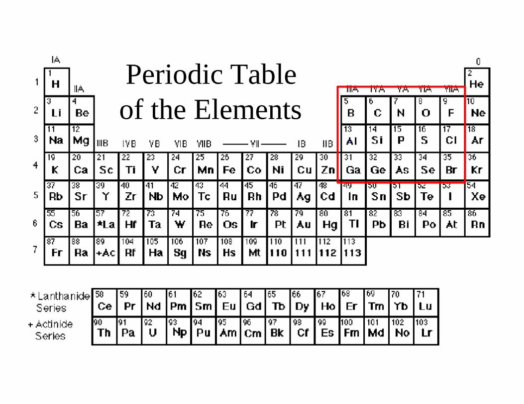
• Silicon and germanium
• Compound semiconductors– SiGe, SiC
– GaAs, InP, etc.
Hong Xiao, Ph. D. www2.austin.cc.tx.us/HongXiao/Book.htm 5
Periodic Tableof the Elements

Hong Xiao, Ph. D. www2.austin.cc.tx.us/HongXiao/Book.htm 6
Semiconductor Substrate and Dopants
Substrate
P-typeDopant
N-type Dopants

Hong Xiao, Ph. D. www2.austin.cc.tx.us/HongXiao/Book.htm 7
Orbital and Energy BandStructure of an Atom
Valence band, Ev
Band gap, Eg
Valence shells
Nuclei
Conducting band, Ec

Hong Xiao, Ph. D. www2.austin.cc.tx.us/HongXiao/Book.htm 8
Band Gap and Resistivity
Eg = 1.1 eV Eg = 8 eV
Aluminum
2.7 µΩ•cm
Sodium
4.7 µΩ•cm
Silicon
~ 1010 µΩ•cm
Silicon dioxide
> 1020 µΩ•cm
Conductors Semiconductor Insulator

Hong Xiao, Ph. D. www2.austin.cc.tx.us/HongXiao/Book.htm 9
Crystal Structure of SingleCrystal Silicon
Si
Si
Si
Si
Si -
Si Si Si
Si
SiSi
Si
Si
Si
Shared electrons

Hong Xiao, Ph. D. www2.austin.cc.tx.us/HongXiao/Book.htm 10
Why Silicon
• Abundant, inexpensive
• Thermal stability
• Silicon dioxide is a strong dielectric andrelatively easy to form
• Silicon dioxide can be used as diffusiondoping mask

Hong Xiao, Ph. D. www2.austin.cc.tx.us/HongXiao/Book.htm 11
N-type (Arsenic) Doped Siliconand Its Donor Energy Band
Electron
-
Si Si Si
Si
SiSi
Si
Si
As
Extra
Valence band, Ev
Eg = 1.1 eV
Conducting band, Ec
Ed ~ 0.05 eV
Hong Xiao, Ph. D. www2.austin.cc.tx.us/HongXiao/Book.htm 12
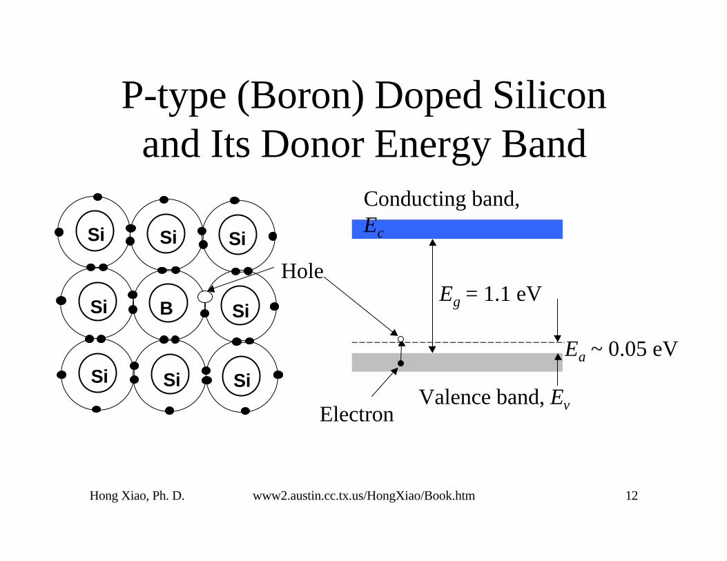
P-type (Boron) Doped Siliconand Its Donor Energy Band
Valence band, Ev
Eg = 1.1 eV
Conducting band,Ec
Ea ~ 0.05 eV
Electron
-
Si Si Si
Si
SiSi
Si
Si
B
Hole

Hong Xiao, Ph. D. www2.austin.cc.tx.us/HongXiao/Book.htm 13
Illustration of Hole Movement
Valence band, Ev
Eg = 1.1 eV
Conducting band, Ec
Ea ~ 0.05 eVElectron
Hole
Electron
HoleValence band, Ev
Eg = 1.1 eV
Conducting band, Ec
Valence band, Ev
Eg = 1.1 eV
Conducting band, Ec
Electron
Hole
Hong Xiao, Ph. D. www2.austin.cc.tx.us/HongXiao/Book.htm 14
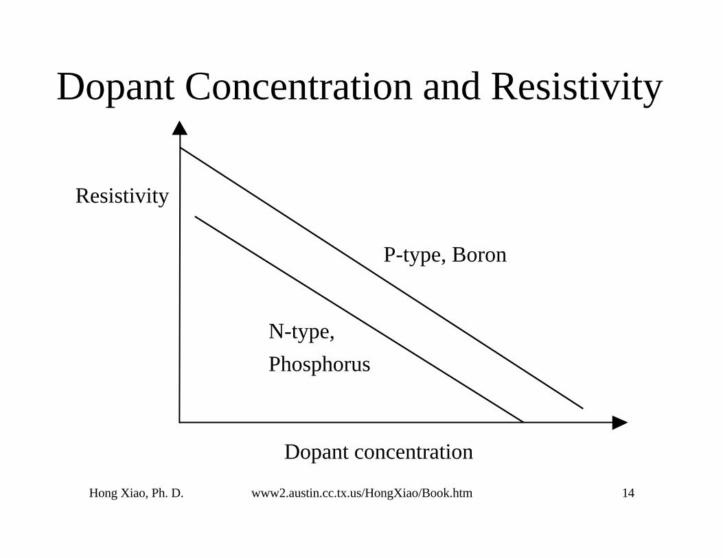
Dopant Concentration and Resistivity
Dopant concentration
Resistivity
P-type, Boron
N-type,
Phosphorus
Hong Xiao, Ph. D. www2.austin.cc.tx.us/HongXiao/Book.htm 15
Dopant Concentration andResistivity
• Higher dopant concentration, more carriers(electrons or holes)
• Higher conductivity, lower resistivity
• Electrons move faster than holes
• N-type silicon has lower resistivity than p-type silicon at the same dopant concentration

Hong Xiao, Ph. D. www2.austin.cc.tx.us/HongXiao/Book.htm 16
Basic Devices
• Resistor
• Capacitor
• Diode
• Bipolar Transistor
• MOS Transistor
Hong Xiao, Ph. D. www2.austin.cc.tx.us/HongXiao/Book.htm 17
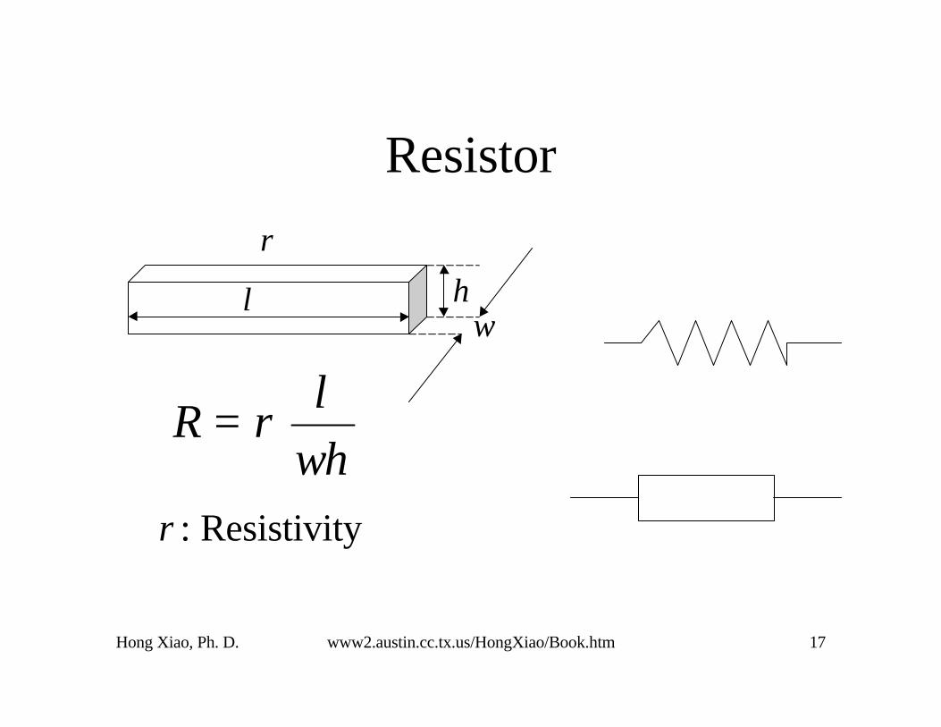
Resistor
l hw
ρ
whl
R ρ=
ρ: Resistivity
Hong Xiao, Ph. D. www2.austin.cc.tx.us/HongXiao/Book.htm 18
Resistor
• Resistors are made by doped silicon orpolysilicon on an IC chip
• Resistance is determined by length, linewidth, height, and dopant concentration

Hong Xiao, Ph. D. www2.austin.cc.tx.us/HongXiao/Book.htm 19
Capacitors
dhl
C κ=h
κ l
d
κ: Dielectric Constant

Hong Xiao, Ph. D. www2.austin.cc.tx.us/HongXiao/Book.htm 20
Capacitors
• Charge storage device
• Memory Devices, esp. DRAM
• Challenge: reduce capacitor size whilekeeping the capacitance
• High-κ dielectric materials
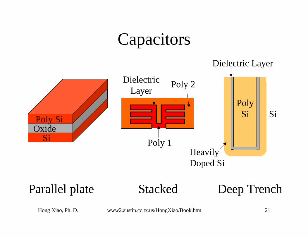
Hong Xiao, Ph. D. www2.austin.cc.tx.us/HongXiao/Book.htm 21
Capacitors
Si
Poly SiOxide
Poly 1
Poly 2DielectricLayer
Dielectric Layer
HeavilyDoped Si
Parallel plate Stacked Deep Trench
PolySi Si

Hong Xiao, Ph. D. www2.austin.cc.tx.us/HongXiao/Book.htm 22
Metal Interconnection and RC Delay
I
Metal, ρDielectric, κ
d
w
l

Hong Xiao, Ph. D. www2.austin.cc.tx.us/HongXiao/Book.htm 23
Diode
• P-N Junction
• Allows electric current go through onlywhen it is positively biased.

Hong Xiao, Ph. D. www2.austin.cc.tx.us/HongXiao/Book.htm 24
Diode
V1 V2
P2P1
• V1 > V2 , • P1 > P2,current current
• V1 < V2 , no current • P1 < P2, no current

Hong Xiao, Ph. D. www2.austin.cc.tx.us/HongXiao/Book.htm 25
P N
+ +
+ +
+ +
+ +
+ +
−−−−−−−−−−
Transition region
V0Vp
Vn
Figure 3.14

Hong Xiao, Ph. D. www2.austin.cc.tx.us/HongXiao/Book.htm 26
Intrinsic Potential
• For silicon V0 ~ 0.7 V
20 lni
da
nNN
qkT
V =

Hong Xiao, Ph. D. www2.austin.cc.tx.us/HongXiao/Book.htm 27
I-V Curve of Diode
V
I
-I0

Hong Xiao, Ph. D. www2.austin.cc.tx.us/HongXiao/Book.htm 28
Bipolar Transistor
• PNP or NPN
• Switch
• Amplifier
• Analog circuit
• Fast, high power device

Hong Xiao, Ph. D. www2.austin.cc.tx.us/HongXiao/Book.htm 29
NPN and PNP Transistors
C
E
B N NP
EB
C
E
C
B P PN
EB
C

Hong Xiao, Ph. D. www2.austin.cc.tx.us/HongXiao/Book.htm 30
NPN Bipolar Transistor
n-epip n+
P-substrate
Electron flow
n+
n+ buried layer
p+p+
SiO2
Al•Cu•SiBase CollectorEmitter

Hong Xiao, Ph. D. www2.austin.cc.tx.us/HongXiao/Book.htm 31
P-substrate
n+ Buried Layer
n Epi
p pFieldoxide
Fieldoxide
CVDoxide
CVDoxide
n+
CVDoxide
Poly
CollectorEmitterBase
Metal
Sidewall Base Contact NPNBipolar Transistor
n+
Fieldoxide
Hong Xiao, Ph. D. www2.austin.cc.tx.us/HongXiao/Book.htm 32
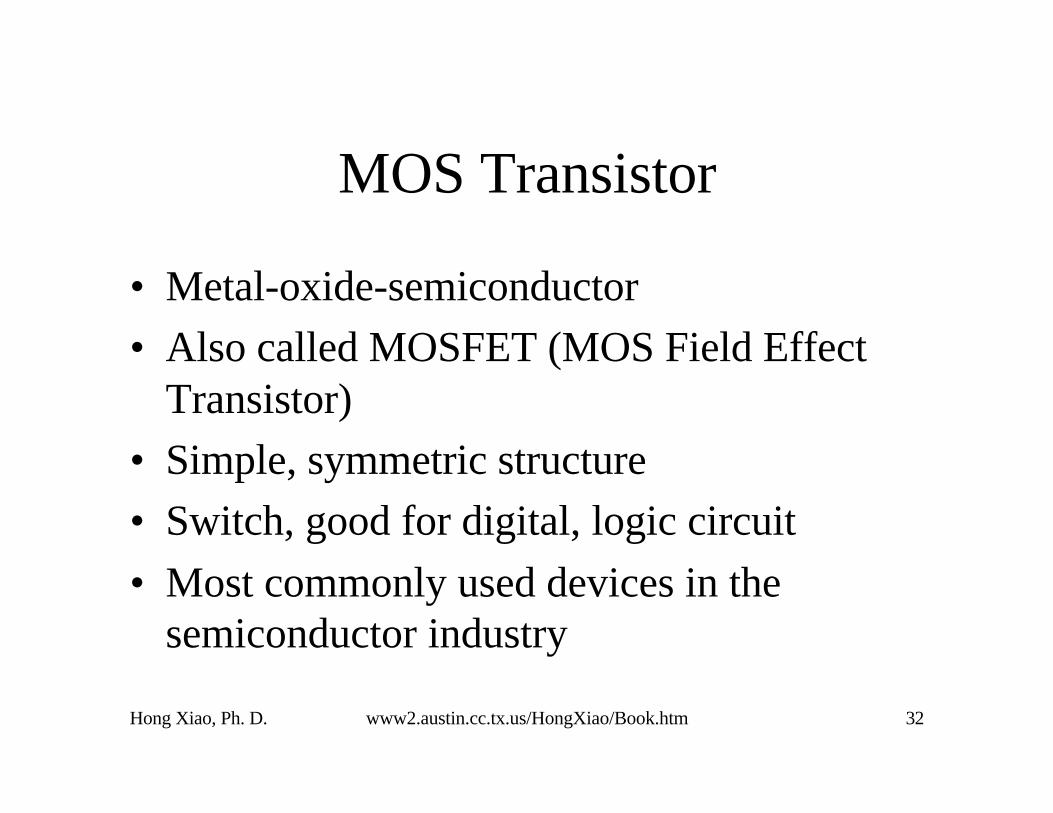
MOS Transistor
• Metal-oxide-semiconductor
• Also called MOSFET (MOS Field EffectTransistor)
• Simple, symmetric structure
• Switch, good for digital, logic circuit
• Most commonly used devices in thesemiconductor industry

Hong Xiao, Ph. D. www2.austin.cc.tx.us/HongXiao/Book.htm 33
NMOS DeviceBasic Structure
VG
VDGroundn+
“Metal” Gate
Source Drainp-Si
n+
VDVG

Hong Xiao, Ph. D. www2.austin.cc.tx.us/HongXiao/Book.htm 34
NMOS Device
+
“Metal” Gate
SiO2
Source Drainp-Si
n+
VD > 0VG > VT > 0
+ + + + + + +− − − − − − −
Electron flow
Positive charges
Negative chargesNo current
n+SiO2
Source Drainp-Si
n+
VDVG = 0
n

Hong Xiao, Ph. D. www2.austin.cc.tx.us/HongXiao/Book.htm 35
PMOS Device
+
“Metal” Gate
SiO2
Source Drainn-Si
p+
VD > 0VG < VT < 0
+ + + + + + +− − − − − − −
Hole flow
Positive charges
Negative charges
No current
p+SiO
2
Source Drainn-Si
p+
VDVG = 0
p

Hong Xiao, Ph. D. www2.austin.cc.tx.us/HongXiao/Book.htm 36
MOSFET
Hong Xiao, Ph. D. www2.austin.cc.tx.us/HongXiao/Book.htm 37
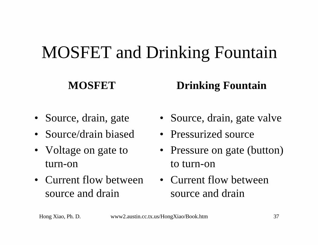
MOSFET and Drinking Fountain
MOSFET
• Source, drain, gate
• Source/drain biased
• Voltage on gate toturn-on
• Current flow betweensource and drain
Drinking Fountain
• Source, drain, gate valve
• Pressurized source
• Pressure on gate (button)to turn-on
• Current flow betweensource and drain

Hong Xiao, Ph. D. www2.austin.cc.tx.us/HongXiao/Book.htm 38
Basic Circuits
• Bipolar
• PMOS
• NMOS
• CMOS
• BiCMOS

Hong Xiao, Ph. D. www2.austin.cc.tx.us/HongXiao/Book.htm 39
Devices with Different Substrates
• Bipolar
• MOSFET
• BiCMOS
Silicon
• GaAs: up to 20 GHz device
• Light emission diode (LED)Compound
• Bipolar: high speed devicesGermanium
DominateIC industry

Hong Xiao, Ph. D. www2.austin.cc.tx.us/HongXiao/Book.htm 40
Market of Semiconductor Products
MOSFET
100%
50%
1980 1990 2000
Compound
Bipolar
88%
8%
4%

Hong Xiao, Ph. D. www2.austin.cc.tx.us/HongXiao/Book.htm 41
Bipolar IC
• Earliest IC chip
• 1961, four bipolar transistors, $150.00
• Market share reducing rapidly
• Still used for analog systems and powerdevices
• TV, VCR, Cellar phone, etc.

Hong Xiao, Ph. D. www2.austin.cc.tx.us/HongXiao/Book.htm 42
PMOS
• First MOS field effect transistor, 1960
• Used for digital logic devices in the 1960s
• Replaced by NMOS after the mid-1970s

Hong Xiao, Ph. D. www2.austin.cc.tx.us/HongXiao/Book.htm 43
NMOS
• Faster than PMOS
• Used for digital logic devices in 1970s and1980s
• Electronic watches and hand-hold calculators
• Replaced by CMOS after the 1980s

Hong Xiao, Ph. D. www2.austin.cc.tx.us/HongXiao/Book.htm 44
CMOS
• Most commonly used circuit in IC chipsince 1980s
• Low power consumption
• High temperature stability
• High noise immunity
• Symmetric design
Hong Xiao, Ph. D. www2.austin.cc.tx.us/HongXiao/Book.htm 45
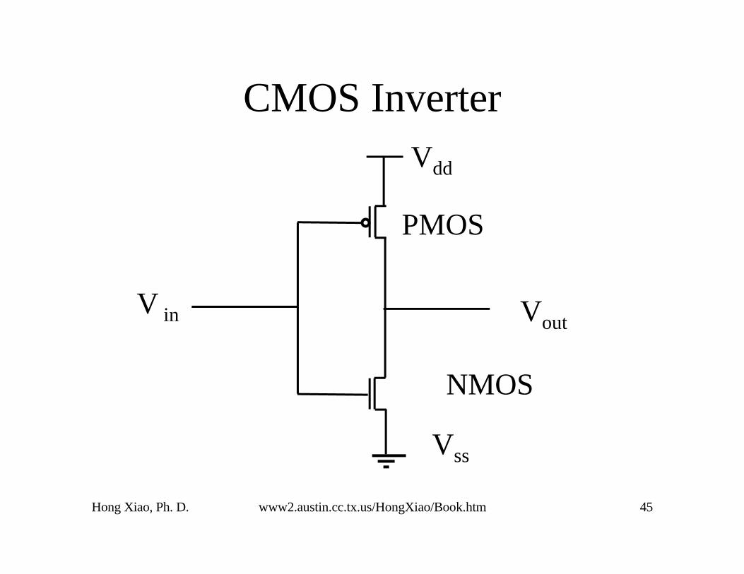
CMOS Inverter
V in Vout
Vdd
Vss
PMOS
NMOS

Hong Xiao, Ph. D. www2.austin.cc.tx.us/HongXiao/Book.htm 46
CMOS IC
p-Si USGn-SiBalk Si
Polysilicon
STI
n+ Source/Drain p+ Source/DrainGate Oxide
Hong Xiao, Ph. D. www2.austin.cc.tx.us/HongXiao/Book.htm 47
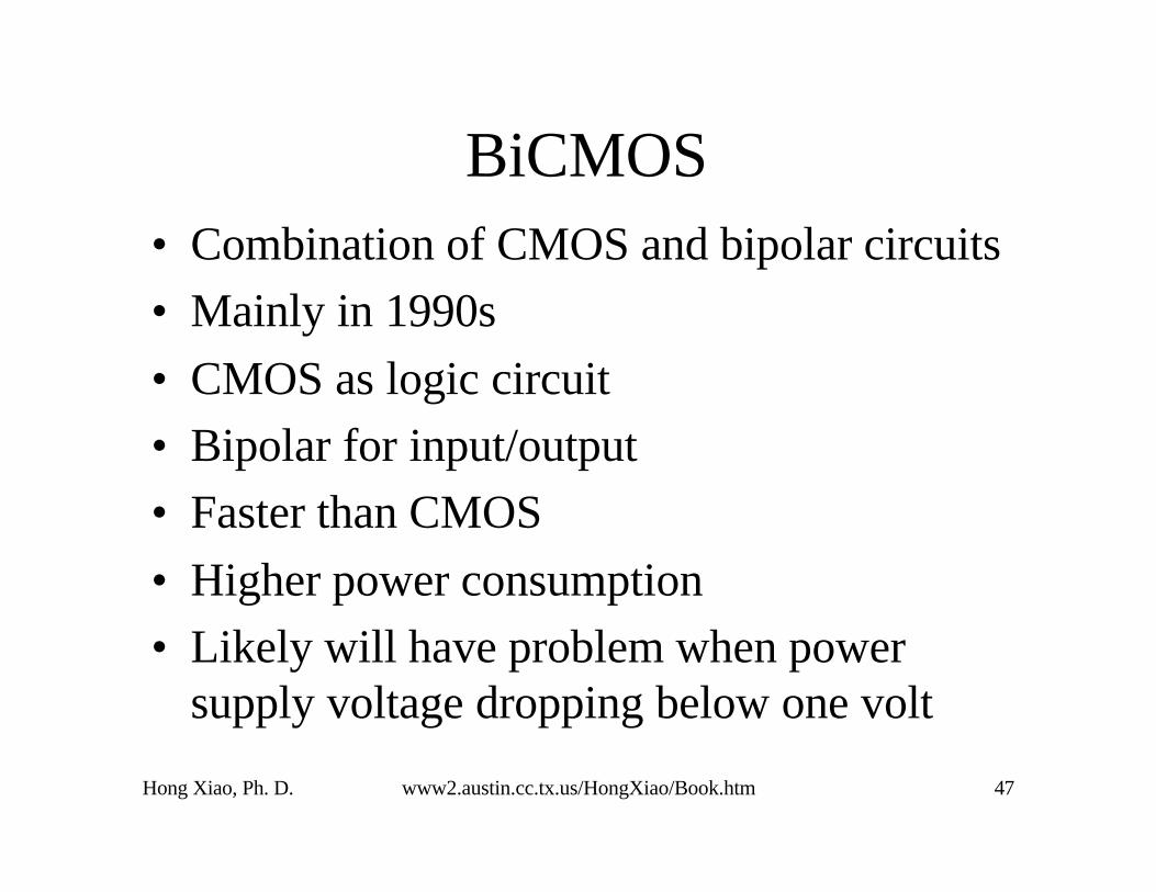
BiCMOS• Combination of CMOS and bipolar circuits
• Mainly in 1990s
• CMOS as logic circuit
• Bipolar for input/output
• Faster than CMOS
• Higher power consumption
• Likely will have problem when powersupply voltage dropping below one volt
Hong Xiao, Ph. D. www2.austin.cc.tx.us/HongXiao/Book.htm 48
IC Chips
• Memory
• Microprocessor
• Application specific IC (ASIC)

Hong Xiao, Ph. D. www2.austin.cc.tx.us/HongXiao/Book.htm 49
Memory Chips
• Devices store data in the form of electric charge
• Volatile memory– Dynamic random access memory (DRAM)
– S random access memory (SRAM)
• Non-volatile memory– Erasable programmable read only memory (EPROM)
– FLASH

Hong Xiao, Ph. D. www2.austin.cc.tx.us/HongXiao/Book.htm 50
DRAM
• Major component of computer and otherelectronic instruments for data storage
• Main driving force of IC processing development
• One transistor, one capacitor

Hong Xiao, Ph. D. www2.austin.cc.tx.us/HongXiao/Book.htm 51
Basic DRAM Memory Cell
Word line
Bit line Vdd
NMOS
Capacitor

Hong Xiao, Ph. D. www2.austin.cc.tx.us/HongXiao/Book.htm 52
SRAM
• Fast memory application such as computer cachememory to store commonly used instructions
• Unit memory cell consists of six transistors
• Much faster than DRAM
• More complicated processing, more expensive

Hong Xiao, Ph. D. www2.austin.cc.tx.us/HongXiao/Book.htm 53
EPROM
• Non-volatile memory
• Keeping data ever without power supply
• Computer bios memory which keeps bootup instructions
• Floating gate
• UV light memory erase

Hong Xiao, Ph. D. www2.austin.cc.tx.us/HongXiao/Book.htm 54
EPROM
n+GateOxide
Source Drainp-Si
n+
VDVG
Poly 1
Poly 2Inter-polyDielectric
PassivationDielectric
Floating Gate
Control Gate
Hong Xiao, Ph. D. www2.austin.cc.tx.us/HongXiao/Book.htm 55
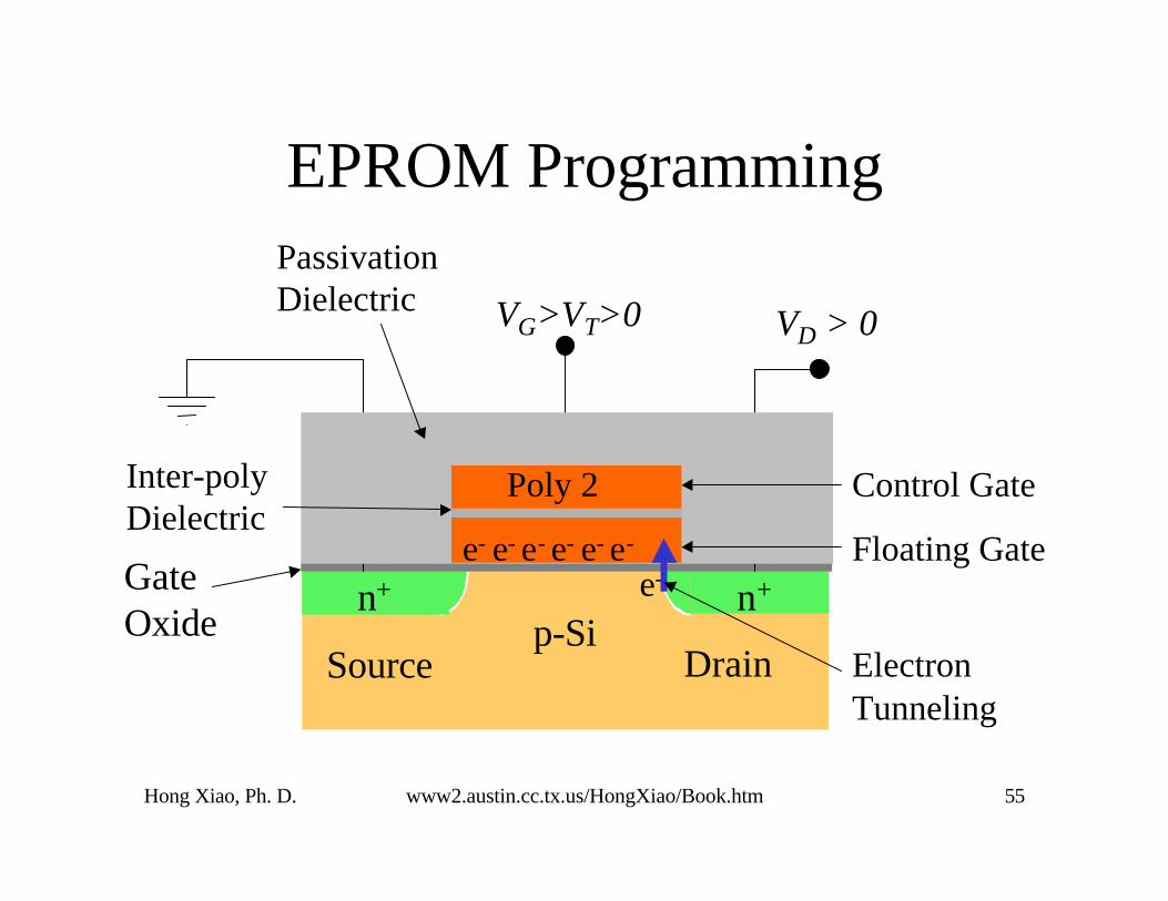
EPROM Programming
n+GateOxide
Source Drainp-Si
n+
Poly 2Inter-polyDielectric
PassivationDielectric
VD > 0VG>VT>0
e- e- e- e- e- e-
e-
ElectronTunneling
Floating Gate
Control Gate

Hong Xiao, Ph. D. www2.austin.cc.tx.us/HongXiao/Book.htm 56
EPROM Programming
n+GateOxide
Source Drainp-Si
n+
Floating Gate
Poly 2 Control GateInter-polyDielectric
PassivationDielectric
VD > 0VG>VT>0
e- e-
UV light
ElectronTunneling

Hong Xiao, Ph. D. www2.austin.cc.tx.us/HongXiao/Book.htm 57
IC Fabrication Processes
IC
Fab.
Adding
Removing
Heating
Patterning
Ion implantation, Diffusion
Grown thin film, SiO 2
Deposited thin film
Wafer Clean
Etch
CMP
Annealing
Reflow
Alloying
Photolithography
CV
PVD
Electrical
Patterned etch
Blanket
Strip Dielectri
Meta
Epi, Poly
Dielectri
Meta
PR coating (adding)
Baking (heating,
Developing
Meta
Oxid
Implantati
Exposure (heating)

Hong Xiao, Ph. D. www2.austin.cc.tx.us/HongXiao/Book.htm 58
Basic Bipolar Process Steps
• Buried layer doping
• Epitaxial silicon growth
• Isolation and transistor doping
• Interconnection
• Passivation

Hong Xiao, Ph. D. www2.austin.cc.tx.us/HongXiao/Book.htm 59
Buried Layer Implantation
P-silicon
SiO2
n+

Hong Xiao, Ph. D. www2.austin.cc.tx.us/HongXiao/Book.htm 60
Epitaxy Grow
P-silicon
n+ buried layer
n-epi
Hong Xiao, Ph. D. www2.austin.cc.tx.us/HongXiao/Book.htm 61
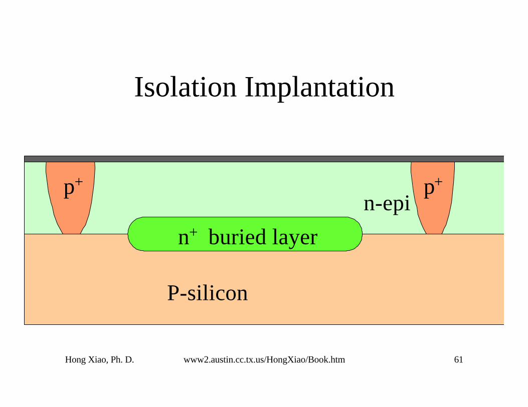
Isolation Implantation
p+
n-epip+
P-silicon
n+ buried layer

Hong Xiao, Ph. D. www2.austin.cc.tx.us/HongXiao/Book.htm 62
Emitter/Collector and BaseImplantation
p+
n-epip+
P-silicon
n+ buried layer
p n+n+
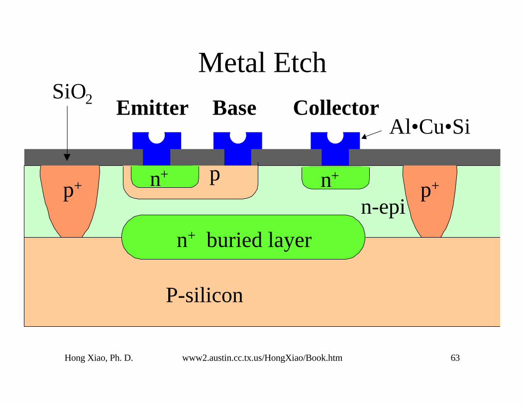
Hong Xiao, Ph. D. www2.austin.cc.tx.us/HongXiao/Book.htm 63
Metal Etch
p+ p+
P-silicon
n+ buried layer
n-epi
Emitter Base CollectorSiO2
Al•Cu•Si
p+n +n

Hong Xiao, Ph. D. www2.austin.cc.tx.us/HongXiao/Book.htm 64
Passivation Oxide DepositionEmitter Base Collector Al•Cu•Si
CVDoxide
SiO2
p+ p+
P-silicon
n+ buried layer
n-epi
p+n +n

Hong Xiao, Ph. D. www2.austin.cc.tx.us/HongXiao/Book.htm 65
MOSFET
• Good for digital electronics
• Major driving forces:– Watches
– Calculators
– PC
– Internet
– Telecommunication

Hong Xiao, Ph. D. www2.austin.cc.tx.us/HongXiao/Book.htm 66
1960s: PMOS Process
• Bipolar dominated
• First MOSFET made in Bell Labs
• Silicon substrate
• Diffusion for doping– Boron diffuses faster in silicon
– PMOS

Hong Xiao, Ph. D. www2.austin.cc.tx.us/HongXiao/Book.htm 67
PMOS Process Sequence (1960s)Wafer clean (R) Etch oxide (R)
Field oxidation (A) Strip photo resist (R)
Mask 1. (Source/Drain) (P) Al deposition (A)
Etch oxide (R) Mask 4. (Metal) (P)
Strip photo resist/Clean (R) Etch Aluminum (R)
S/D diffusion (B)/Oxidation (A) Strip photo resist (R)
Mask 2. (Gate) (P) Metal Anneal (H)
Etch oxide (R) CVD oxide (A)
Strip photo resist/Clean (R) Mask 5. (Bonding pad) (P)
Gate oxidation (A) Etch oxide (R)
Mask 3. (Contact) (P) Test and packaging
Hong Xiao, Ph. D. www2.austin.cc.tx.us/HongXiao/Book.htm 68
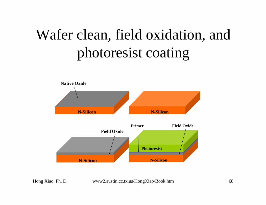
Wafer clean, field oxidation, andphotoresist coating
N-Silicon
Native Oxide
N-Silicon
N-Silicon
Field Oxide
N-Silicon
Primer
Photoresist
Field Oxide

Hong Xiao, Ph. D. www2.austin.cc.tx.us/HongXiao/Book.htm 69
Photolithography and etch
N-Silicon
Source/Drain Mask
Photoresist
Field Oxide
N-Silicon
Source/Drain Mask
PR
UV Light
N-Silicon
PR
Field Oxide
N-Silicon
PR
Field Oxide

Hong Xiao, Ph. D. www2.austin.cc.tx.us/HongXiao/Book.htm 70
Source/drain doping and gateoxidation
N-Silicon
Field Oxide
N-Siliconp+ p+
Field Oxide
N-Siliconp+ p+
Field Oxide
N-Siliconp+ p+
Gate Oxide Field Oxide

Hong Xiao, Ph. D. www2.austin.cc.tx.us/HongXiao/Book.htm 71
Contact, Metallization, andPassivation
N-Siliconp+ p+
Gate Oxide Field Oxide
N-Siliconp+ p+
Gate Oxide Field OxideAl·Si
N-Siliconp+
Gate Oxide Field Oxide
p+
N-Siliconp+
Gate Oxide CVD Cap Oxide
p+
Hong Xiao, Ph. D. www2.austin.cc.tx.us/HongXiao/Book.htm 72
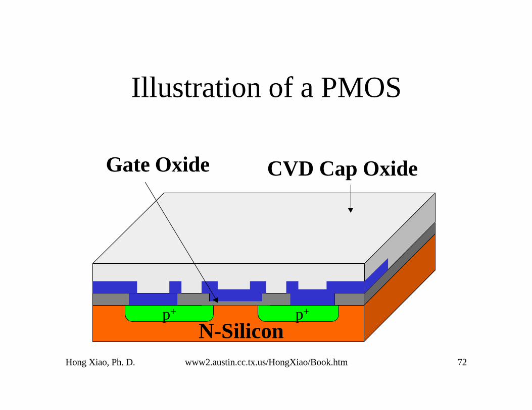
Illustration of a PMOS
N-Silicon
Gate Oxide CVD Cap Oxide
p+p+

Hong Xiao, Ph. D. www2.austin.cc.tx.us/HongXiao/Book.htm 73
NMOS Process after mid-1970s
• Doping: ion implantation replaced diffusion
• NMOS replaced PMOS– NMOS is faster than PMOS
• Self-aligned source/drain
• Main driving force: watches and calculators
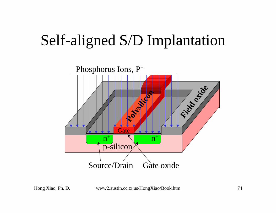
Hong Xiao, Ph. D. www2.austin.cc.tx.us/HongXiao/Book.htm 74
p-silicon
Fiel
d ox
ide
Gate
Source/Drain Gate oxide
Phosphorus Ions, P+
n+ n+
Polys
ilico
n
Self-aligned S/D Implantation

Hong Xiao, Ph. D. www2.austin.cc.tx.us/HongXiao/Book.htm 75
NMOS Process Sequence (1970s)Wafer clean PSG reflow
Grow field oxide Mask 3. Contact
Mask 1. Active Area Etch PSG/USG
Etch oxide Strip photo resist/Clean
Strip photo resist/Clean Al deposition
Grow gate oxide Mask 4. Metal
Deposit polysilicon Etch Aluminum
Mask 2. Gate Strip photo resist
Etch polysilicon Metal anneal
Strip photo resist/Clean CVD oxide
S/D and poly dope implant Mask 5. Bonding pad
Anneal and poly reoxidation Etch oxide
CVD USG/PSG Test and packaging

Hong Xiao, Ph. D. www2.austin.cc.tx.us/HongXiao/Book.htm 76
NMOS Process Sequence
Clean
OxideEtch
Poly Dep.
P+ IonImplant
FieldOxidation
GateOxidation
Poly Etch
Annealing
p-Si
n+ n+
p-Si
p-Si p-Si
poly poly
polypoly
p-Si p-Si
p-Si p-Si

Hong Xiao, Ph. D. www2.austin.cc.tx.us/HongXiao/Book.htm 77
NMOS Process Sequence
PSGEtch
MetalEtch
MetalDep.
NitrideDep.
PSG Dep.PSGReflow
n+ n+
poly
poly
poly
poly
poly
polyPSG
PSG
PSG PSG
PSG
PSG
Al·Si
Al·SiAl·Si
SiN
p-Si
p-Si
p-Si
p-Si
p-Si
p-Si

Hong Xiao, Ph. D. www2.austin.cc.tx.us/HongXiao/Book.htm 78
CMOS
• In the 1980s MOSFET IC surpassed bipolar
• LCD replaced LED
• Power consumption of circuit
• CMOS replaced NMOS
• Still dominates the IC market
• Backbone of information revolution

Hong Xiao, Ph. D. www2.austin.cc.tx.us/HongXiao/Book.htm 79
Advantages of CMOS
• Low power consumption
• High temperature stability
• High noise immunity

Hong Xiao, Ph. D. www2.austin.cc.tx.us/HongXiao/Book.htm 80
CMOS Inverter, Its LogicSymbol and Logic Table
Vin Vout
Vss
VddVin Vout
PMOS
NMOS In Out
0 1
1 0

Hong Xiao, Ph. D. www2.austin.cc.tx.us/HongXiao/Book.htm 81
CMOS Chip with 2 Metal Layers
P-type substrate
p+p+
N-well
SiO2LOCOSBPSG
Al·Cu·Si
Metal 2, Al·Cu·Si
NitrideOxide
USG dep/etch/dep
Poly Si Gate
IMD
PMD
PD2PD1
p+ p+n+n+

Hong Xiao, Ph. D. www2.austin.cc.tx.us/HongXiao/Book.htm 82
FSG
Metal 4 Copper
Passivation 1, USGPassivation 2, nitride
Lead-tinalloy bump
FSG
CopperMetal 2
FSG
FSG
CopperMetal 3
FSG
P-epiP-wafer
N-wellP-welln+STI p+ p+USGn+
PSG Tungsten
FSGCu Cu
Tantalumbarrier layer
Nitride etchstop layer
Nitrideseal layer
M 1
Tungsten localInterconnection
Tungsten plug
PMD nitridebarrier layer
T/TiN barrier &adhesion layer
Tantalumbarrier layer
CMOS Chipwith 4 MetalLayers

Hong Xiao, Ph. D. www2.austin.cc.tx.us/HongXiao/Book.htm 83
Summary
• Semiconductors are the materials withconductivity between conductor andinsulator
• Its conductivity can be controlled by dopantconcentration and applied voltage
• Silicon, germanium, and gallium arsenate
• Silicon most popular: abundant and stableoxide

Hong Xiao, Ph. D. www2.austin.cc.tx.us/HongXiao/Book.htm 84
Summary
• Boron doped semiconductor is p-type,majority carriers are holes
• P, As, or Sb doped semiconductor is p-type,the majority carriers are electrons
• Higher dopant concentration, lower resistivity
• At the same dopant concentration, n-type haslower resistivity than p-type

Hong Xiao, Ph. D. www2.austin.cc.tx.us/HongXiao/Book.htm 85
Summary
• R=ρ l/A• C=κ A/d• Capacitors are mainly used in DRAM
• Bipolar transistors can amplify electric signal,mainly used for analog systems
• MOSFET electric controlled switch, mainlyused for digital systems

Hong Xiao, Ph. D. www2.austin.cc.tx.us/HongXiao/Book.htm 86
Summary
• MOSFETs dominated IC industry since 1980s
• Three kinds IC chips microprocessor,memory, and ASIC
• Advantages of CMOS: low power, hightemperature stability, high noise immunity,and clocking simplicity

Hong Xiao, Ph. D. www2.austin.cc.tx.us/HongXiao/Book.htm 87
Summary
• The basic CMOS process steps are transistormaking (front-end) andinterconnection/passivation (back-end)
• The most basic semiconductor processes areadding, removing, heating, and patterningprocesses.


![[Psy] ch03](https://static.fdocuments.in/doc/165x107/555d741ad8b42a687b8b53c6/psy-ch03.jpg)