Chapter 14 Low-Dimensional Nanostructureshomepages.wmich.edu/~leehs/ME695/Chapter 14.pdfusing...
30
14-1 Chapter 14 Low-Dimensional Nanostructures Contents Chapter 14 Low-Dimensional Nanostructures ............................................................. 14-1 Contents .......................................................................................................................... 14-1 14.1 Low-Dimensional Systems ................................................................................ 14-2 14.1.1 Quantum Well (2D) ................................................................................... 14-3 Example 14.1 Energy Levels of a Quantum Well ...................................................... 14-9 14.1.2 Quantum Wires (1D)................................................................................ 14-10 14.1.3 Quantum Dots (0D).................................................................................. 14-15 14.1.4 Thermoelectric Transport Properties of Quantum Wells ......................... 14-17 14.1.5 Thermoelectric Transport Properties of Quantum Wires......................... 14-19 14.1.6 Proof-of-Principle Studies ....................................................................... 14-22 14.1.7 Size effects of Quantum Well on Lattice Thermal Conductivity ............ 14-25 Problems ....................................................................................................................... 14-29 References..................................................................................................................... 14-30
Transcript of Chapter 14 Low-Dimensional Nanostructureshomepages.wmich.edu/~leehs/ME695/Chapter 14.pdfusing...

14-1
Chapter 14 Low-Dimensional
Nanostructures
Contents
Chapter 14 Low-Dimensional Nanostructures ............................................................. 14-1
Contents .......................................................................................................................... 14-1
14.1 Low-Dimensional Systems ................................................................................ 14-2
14.1.1 Quantum Well (2D) ................................................................................... 14-3
Example 14.1 Energy Levels of a Quantum Well ...................................................... 14-9
14.1.2 Quantum Wires (1D)................................................................................ 14-10
14.1.3 Quantum Dots (0D).................................................................................. 14-15
14.1.4 Thermoelectric Transport Properties of Quantum Wells ......................... 14-17
14.1.5 Thermoelectric Transport Properties of Quantum Wires......................... 14-19
14.1.6 Proof-of-Principle Studies ....................................................................... 14-22
14.1.7 Size effects of Quantum Well on Lattice Thermal Conductivity ............ 14-25
Problems ....................................................................................................................... 14-29
References ..................................................................................................................... 14-30

14-2
The field of thermoelectrics advanced rapidly in the 1950s when the basic science of thermoelectric
materials became well established, the important role of heavily doped semiconductors as good
thermoelectric materials became accepted, the thermoelectric material bismuth telluride was
discovered and developed for commercialization, and the thermoelectric industry was launched.
Over the following three decades, 1960 to 1990, only incremental gains were made in increasing
ZT, with bismuth telluride, remaining the best commercial material at ZT ≈ 1. During that three-
decade period, the thermoelectrics field received little attention from the worldwide scientific
research community. Nevertheless, the thermoelectric industry grew slowly but steadily by finding
niche applications for space missions and medical applications, where cost and efficiency were
not as important as energy availability, reliability, and predictability.
The present interest in low-dimensional thermoelectric materials was prompted by the
theoretical work of Hicks and Dresselhaus (1993)[1-3], stimulating the research community to
once again become active in this field and to find new research directions that would have an
impact on future developments and lead to thermoelectric materials with better performance. As a
result of this stimulation, two different research approaches were taken for developing the next
generation of thermoelectric materials, one using new families of bulk materials and the other
using low-dimensional materials systems.
14.1 Low-Dimensional Systems
As the dimensionality is decreased from 3D crystal solids to two-dimensional quantum wells (2D)
to one-dimensional (1D) quantum wires, and finally to zero-dimensional quantum dots (0D), new
physical phenomena are introduced and new opportunities arise to vary the thermoelectric
transport coefficients (, and k), independently. For example, it is known that we can have a
transition from a semimetal (bismuth) to a semiconductor by increasing the conduction band edge
with quantum confinement. Furthermore, the introduction of many interfaces offers the
opportunity to increase phonon scattering more than electron scattering so that the electrical

14-3
conductivity is not changed much while the thermal conductivity is much reduced by interface
scattering processes.
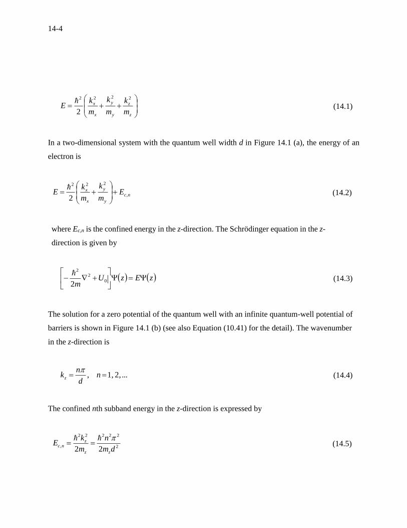
14.1.1 Quantum Well (2D)
Quantum effects arise in systems which confine electrons to regions comparable to their de
Broglie wavelength. When such confinement occurs in one dimension only (say, by a restriction
on the motion of the electron in the z-direction), with free motion in the x- and y-directions, a
two-dimensional system is created, which is shown in Figure 14.1 (a).
(a)
(b)
Figure 14.1 (a) Schematic presentation of a quantum well (2D), and (b) the quantum numbers of
an electron in the quantum well.
The dispersion relation for electrons in a three-dimensional (3D) system is given by
xy
z
d
L
L
E
z
n = 1
n = 2
n = 3
d
U0 = ?
U0 = 0
14-4
z
z
y
y
x
x
m
k
m
k
m
kE
2222
2
(14.1)
In a two-dimensional system with the quantum well width d in Figure 14.1 (a), the energy of an
electron is
nc
y
y
x
x Em
k
m
kE ,
222
2
(14.2)
where Ec,n is the confined energy in the z-direction. The Schrödinger equation in the z-
direction is given by
zEzUm
0
22
2
(14.3)
The solution for a zero potential of the quantum well with an infinite quantum-well potential of
barriers is shown in Figure 14.1 (b) (see also Equation (10.41) for the detail). The wavenumber
in the z-direction is
... 2, 1, , nd
nkz
(14.4)
The confined nth subband energy in the z-direction is expressed by
2
22222
,22 dm
n
m
kE
zz
znc
(14.5)

14-5
From Equation (14.2), the total kinetic energy of an electron is then expressed by
2
222222
22 dm
n
m
k
m
kE
zy
y
x
x
(14.6)
Density of States in 2D
We here develop the density of states in a two-dimensional system. The total energy of an
electron is expressed by introducing arbitrary k’ and m’ as
2
22222222
222 dm
n
m
k
m
k
m
kE
z
yx
(14.7)
We can relate the arbitrary parameters to the original parameters from Equation (14.6) as
m
k
m
k x
x
x
22
, which leads to xx
x km
mk
(14.8)
m
k
m
k y
y
y
22
, which leads to y
y
y km
mk
(14.9)
In the strictly two-dimensional system, we have
kdkm
mmkdkd
m
mmdkdkdk
yx
yx
yx
yx
2
(14.10)

14-6
The area of the smallest wavevector in a 2D crystal is 22 L . The number of states between k
and k + dk in the perfect two-dimensional space is then obtained as
kdm
mm
L
kdkkN
yx
22
22)(
(14.11)
where the factor of 2 accounts for the electron spin (Pauli Exclusion Principle). Now the density
of states per unit area is
kdm
mmk
L
dkkNdkkg
yx
2
)()(
(14.12)
From Equation (14.7), we have
2
1
2
1
2 Emk
(14.13)
Differentiating this gives
2
12
1
2
2
Em
dE
kd
(14.14)
Inserting Equations (14.13) and (14.14) into (14.12), the 2D density of states per unit area for
each allowable kxy series is
20 )(
dmEg
(14.15)
14-7
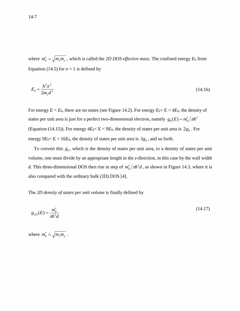
where yxd mmm , which is called the 2D DOS effective mass. The confined energy E0 from
Equation (14.5) for n = 1 is defined by
2
22
02 dm
Ez
(14.16)
For energy E < E0, there are no states (see Figure 14.2). For energy E0< E < 4E0, the density of
states per unit area is just for a perfect two-dimensional electron, namely 2
0 )( dmEg
(Equation (14.15)). For energy 4E0< E < 9E0, the density of states per unit area is 02g . For
energy 9E0< E < 16E0, the density of states per unit area is 03g , and so forth.
To convert this 0g , which is the density of states per unit area, to a density of states per unit
volume, one must divide by an appropriate length in the z-direction, in this case by the wall width
d. This three-dimensional DOS then rise in step of dmd
2 , as shown in Figure 14.3, where it is
also compared with the ordinary bulk (3D) DOS [4].
The 2D density of states per unit volume is finally defined by
d
mEg d
D 22 )(
(14.17)
where yxd mmm .

14-8
Figure 14.2 Energy versus wavenumber k for a quasi-quantum well [4].
Figure 14.3 Density of states for a quasi-quantum well. The corresponding density of states for
an unconfined 3D system is also shown for comparison (broken line). E0 is defined in Equation
(14.16) [4].
The most popular strategy for design is to take advantage of the enhanced density of states for
electrons near the Fermi energy due to the reduced dimensionality. A quantum well can be
14-9
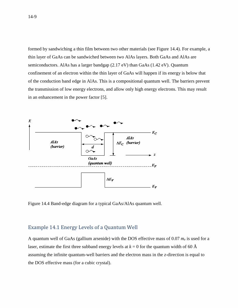
formed by sandwiching a thin film between two other materials (see Figure 14.4). For example, a
thin layer of GaAs can be sandwiched between two AlAs layers. Both GaAs and AlAs are
semiconductors. AlAs has a larger bandgap (2.17 eV) than GaAs (1.42 eV). Quantum
confinement of an electron within the thin layer of GaAs will happen if its energy is below that
of the conduction band edge in AlAs. This is a compositional quantum well. The barriers prevent
the transmission of low energy electrons, and allow only high energy electrons. This may result
in an enhancement in the power factor [5].
Figure 14.4 Band-edge diagram for a typical GaAs/AlAs quantum well.
Example 14.1 Energy Levels of a Quantum Well
A quantum well of GaAs (gallium arsenide) with the DOS effective mass of 0.07 me is used for a
laser, estimate the first three subband energy levels at k = 0 for the quantum width of 60 Å
assuming the infinite quantum-well barriers and the electron mass in the z-direction is equal to
the DOS effective mass (for a cubic crystal).

14-10
Solution:
From Equation (14.6) at k = 0 with dz mm , the nth subband energy with the infinite quantum-
well barriers is
2
222
2 dm
nE
d
For n = 1
eVeVJmkg
JsE 149.0
/106021.11060101093.907.02
1210626.61921031
22234
Likewise,
E = 0.597 eV for n = 2
E = 1.343 eV for n = 3
Comments: It is seen that the conduction band edge of the quantum well is lifted up 0.149 eV
from the conduction band edge of a bulk material. This lift-up may be useful in enhancing the
thermoelectric performance. The first three subband energy levels are calculated with the
assumption of the infinite barrier potential. The lowest subband is most important due to the
closeness of the Fermi energy. If the barrier potential around the quantum well is finite, the
energy levels may be more complicated than given by Equation (14.6).
14.1.2 Quantum Wires (1D)

14-11
Quantum effects in systems which confine electrons to regions comparable to their de Broglie
wavelength. When such confinement occurs in two dimensions only (say, by two restrictions on
the motion of the electron in the z- and y-directions), with free motion in the x-direction, a one-
dimensional electron is created, which is shown in Figure 14.5.
Figure 14.5 Schematic presentation of a quantum wire.
In a one-dimensional system for a quantum wire, the total energy is
2
222
2
22222
222 dm
l
dm
n
m
kE
zyx
x (14.18)
where n = 1, 2….. and l = 1, 2, …
Density of States in 1D
We here develop the density of states in a strict one-dimensional system. The total energy of an
electron is
2
222
2
2222222
2222 dm
l
dm
n
m
k
m
kE
zy
x
(14.19)
d
Lz
y
x

14-12
We can relate the arbitrary parameter to the original parameter in Equation (14.18).
m
k
m
k x
x
x
22
, which leads to xx
x km
mk
(14.20)
In the strictly one-dimensional system, we have
xx kd
m
mdk
(14.21)
The length of the smallest wavevector in a 1D crystal is L2 . The number of states between k
and k + dk in the one-dimensional space is then obtained as
xx kd
m
m
L
dkkN
2
2)(
(14.22)
where the factor of 2 accounts for the electron spin (Pauli Exclusion Principle). The
density of states per unit length is
xx kd
m
m
L
dkkNdkkg
1)()(
(14.23)
From Equation (14.19), we have
2
1
2
1
2 Emk
(14.24)

14-13
Differentiating this gives
2
12
1
2
2
Em
dE
kd
(14.25)
Inserting Equations (14.24) and (14.25) into (14.23), we have
2
12
1
20
2
2
1)(
E
mEg d
(14.26)
where xd mm . The confined energy E0 from Equation (14.18) for n = l = 1 is
2
22
2
22
022 dmdm
Ezy
(14.27)
The 1D density of states per unit volume with considering (n+l=2) is finally obtained by
2
12
1
221
21)(
E
m
dEg d
D
(14.28)
where xd mm , which is called the 1D DOS effective mass.

14-14
Figure 14.6 Energy versus wavenumber k for a quasi-quantum wire.
Figure 14.7 Density of states for a quasi-quantum wire. The corresponding density of states for
an unconfined 3D system is also shown for comparison (broken line).
Figure 14.7 shows the density of states for such an ideal quantum wire, showing the
characteristic singularity in E-1/2 which was derived for 1D as shown in Equation (14.26). In a
quantum wire, such a singularity will occur at each energy of quantization in the x-direction. For
14-15
real quantum wires, the spacing of the quantized energies and the corresponding wavefunctions,
will depend on the precise shape of the potential U0 in Equation (14.3).
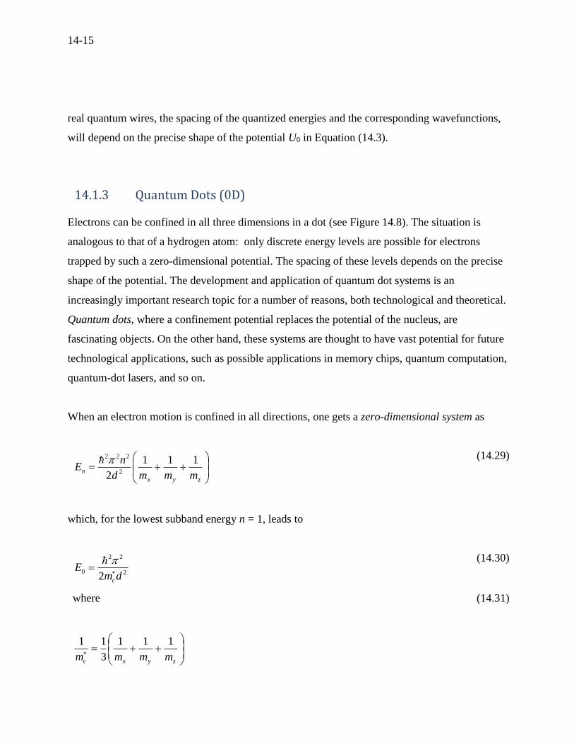
14.1.3 Quantum Dots (0D)
Electrons can be confined in all three dimensions in a dot (see Figure 14.8). The situation is
analogous to that of a hydrogen atom: only discrete energy levels are possible for electrons
trapped by such a zero-dimensional potential. The spacing of these levels depends on the precise
shape of the potential. The development and application of quantum dot systems is an
increasingly important research topic for a number of reasons, both technological and theoretical.
Quantum dots, where a confinement potential replaces the potential of the nucleus, are
fascinating objects. On the other hand, these systems are thought to have vast potential for future
technological applications, such as possible applications in memory chips, quantum computation,
quantum-dot lasers, and so on.
When an electron motion is confined in all directions, one gets a zero-dimensional system as
zyx
nmmmd
nE
111
2 2
222
(14.29)
which, for the lowest subband energy n = 1, leads to
2
22
02 dm
Ec
(14.30)
where
zyxc mmmm
111
3
11
(14.31)

14-16
which is called the conductivity effective mass (see also Equation (12.55)). The density
of states is a series of -function peaks as shown in Figure 14.9.
00 EEEg D (14.32)
Figure 14.8 Schematic presentation of a quantum dot.
Figure 14.9 Density of states for a quasi-quantum dot. The corresponding density of states for an
unconfined 3D system is also shown for comparison (broken line).
d
z
x
y

14-17
14.1.4 Thermoelectric Transport Properties of Quantum Wells
The thermoelectric transport properties are sought assuming that electrons occupy only the
lowest (n = 1) subband of a quantum well. A power law model is used to calculate the
thermoelectric transport properties of a quantum well. The electron relaxation time is expressed
by
rE 0 (14.33)
where r is the scattering parameter. The density of states for the quantum well from Equation
(14.17) is given by
d
mEg d
D 22 )(
(14.34)
For simplicity, the Fermi integral for the quantum well is defined by
0 10 dE
e
EF
FEE
s
s (14.35)
where the reduced energy is TkEE B, the reduced Fermi energy of the quantum well
TkEEE BFF 0
0 and the lowest subband energy 222
0 2 dmE z .
The electron concentration n in thermal equilibrium is

14-18
0
2
0
021
0 dEe
Tk
d
mdEEfEgn
FEE
BdD
(14.36)
which is reduced to
02
2
2F
Tkm
d
Nn Bdv
(14.37)
The electrical conductivity for the quantum well is expressed by
xr
c
Bdv neF
Fr
m
eeF
Tkm
d
N
0
002
12
2
(14.38)
where 21
yxd mmm and 1
115.0 yxc mmm . The Seebeck coefficient for the quantum
well is expressed by
01
1
2F
r
rB EFr
Fr
e
k (14.39)
The Lorentz number for the quantum well is obtained by
2
12
2
1
2
1
3
r
r
r
rBo
Fr
Fr
Fr
Fr
e
kL (14.40)
and the electronic thermal conductivity of the quantum well is expressed as

14-19
oe LTk (14.41)
The dimensionless figure of merit for the quantum well is obtained as
r
rr
rF
r
r
D
Fr
FrFr
FEFr
Frr
ZT
1
23
1
1
21
2
1
2
2
2
01
2
(14.42)
where is the material parameter for the quantum well as
lc
BBdvD
km
TkTkm
d
N
0
2
22
2
2
(14.43)
Equations (14.38) to (14.43) become identical to the formulae of Hicks and Dresselhaus
(1993)[2] when the scattering parameter is assumed to be r = 0.
14.1.5 Thermoelectric Transport Properties of Quantum Wires
The thermoelectric transport properties are sought assuming that electrons occupy only the
lowest (n = 1) subband of quantum well. The power law model is used to calculate the
thermoelectric transport properties of quantum wires. The electron relaxation time is expressed
by
rE 0 (14.44)
where r is the scattering parameter. The density of states for the quantum wires from Equation
(14.28) is given by

14-20
2
12
1
221
2)(
E
m
d
NEg dv
D
(14.45)
where xd mm .
For simplicity, the Fermi integral for the quantum wire is defined by
0 10 dE
e
EF
FEE
s
s (14.46)
where the reduced energy is TkEE B, the reduced Fermi energy of the quantum wire
TkEEE BFF 0
0 and the lowest subband energy for n = 1 (assumption) as
2
22
2
22
022 dmdm
Ezy
(14.47)
The electron concentration n in thermal equilibrium is
0
2
1
2
12
1
22
0
021
20 dE
e
TkTkE
m
d
NdEEfEgn
FEE
BB
dvD
(14.48)
(editor note: in the above equation, change g2D –> g1D)
which is reduced to

14-21
21
21
22
2
F
Tkm
d
Nn Bxv
(14.49)
The electrical conductivity for the quantum wires is expressed by
x
r
x
Bxv neF
Fr
m
eeF
Tkm
d
N
21
21021
21
22 2
12
2
(14.50)
The Seebeck coefficient for the quantum wire is expressed by
0
21
21
2
1
2
3
F
r
r
B E
Fr
Fr
e
k (14.51)
The Lorentz number for the quantum wire is obtained by
2
21
2
1
21
2
32
2
1
2
3
2
1
2
5
r
r
r
rB
o
Fr
Fr
Fr
Fr
e
kL (14.52)
and the electronic thermal conductivity of the quantum wire is expressed as
oe LTk (14.53)
The dimensionless figure of merit for the quantum wire is obtained as

14-22
21
2
21
2
2
3
21
2
0
21
21
1
2
1
2
3
2
51
2
1
2
3
2
1
r
r
r
rF
r
r
D
Fr
Fr
Fr
FE
Fr
Fr
r
ZT
(14.54)
where is the material parameter for the quantum wire,
l
B
x
BvD
k
Tk
m
Tk
d
N 0
221
221
22
(14.55)
Equations (14.50) to (14.55) become identical to the formulae of Hicks and Dresselhaus
(1993)[3] when the scattering parameter is assumed to be constant as r = 0.
14.1.6 Proof-of-Principle Studies
For a specific value of the material parameter , the dimensionless figure of merit within the
quantum well or wire is optimized by varying the electron concentration (or equivalently the
Fermi energy) of the system (Figure 14.10). The higher the value, the higher the optimal ZT
value. Therefore, the quantity provides a guideline for selecting good thermoelectric materials
and for designing optimum quantum wire thermoelectric materials.

14-23
Figure 14.10 The dimensionless figure of merit versus electron concentration for bulk Bi2Te3.
Figure 14.11 Calculated dependence of ZT at room temperature within the quantum well or
within the quantum wire (width d) for Bi2Te3 at the optimum doping concentration for transport
in the highest mobility direction. Also shown is the ZT for bulk Bi2Te3 calculated using the
corresponding bulk model. This plot is based on Hicks (1996) [6].

14-24
The following data were used in Figure 14.11. Bi2Te3 has a trigonal structure, which can be
expressed in terms of a hexagonal unit cell of lattice parameters a0 = 4.3 Å and c0 = 30.5 Å. The
compound has an anisotropic effective mass tensor, with components mx = 0.02 me, my = 0.08 me,
and mz = 0.32 me. The lattice thermal conductivity is kl = 1.5 W/mK and the electron mobility is
x = 1200 cm2/Vs. The degeneracy of valleys is Nv = 6 [7].
Using these simple assumptions, a substantial enhancement was calculated for ZT within the
quantum well for 2D systems having small quantum well widths relative to their bulk sizes. To
make these calculations more useful, we show in Figure 14.11, the enhancement of ZT within a
Bi2Te3 quantum well as a function of d, and an even greater enhancement in ZT is predicted for
Bi2Te3 when prepared as a 1D quantum wire [2, 3, 6]. The results of Figure 14.11 suggest that a
good thermoelectric material in 3D might be expected to exhibit even higher ZT values in reduced
dimensions. To make a fair comparison between 3D and lower dimensions, all ZT values in Figure
14.11 are given for the optimum electron concentration.
Figure 14.12 S2n results (S is in this book) for PbTe/Pb0.927Eu0.073Te multiple-quantum-well
(MQW) structures (full circles) as a function of well thickness d at 300 K. For comparison, the
best experimental bulk PbTe value is also shown. Calculated results for optimum doping using
the model are shown as a solid line. Reprinted from Hicks et al. (1996)[8] with permission.

14-25
According to the model, the increase in Z due to 2D effects arises mainly from the power factor
2n, while the lattice thermal conductivity kl is assumed to be unchanged from the bulk value. In
fact, it is also assumed that mobility in the quantum well is the same as in the bulk. So any
increase in Z would arise through the power factor, where n is the electron concentration in the
quantum well. Therefore, according to the model, we should be able to observe an increase in
2n as the well width is narrowed. The reason for making the comparison between theory and
experiment for 2n rather than 2 is to test the validity of the theoretical model in terms of
intrinsic phenomena rather than phenomena sensitive to materials processing conditions that
more strongly influence the electron mobility.
Samples were grown by molecular-beam epitaxy (MBE). Details of the sample preparation are
given in Harman et al. (1996) [9]. Superlattice samples with 100 periods of the multiple-quantum-
well structures were grown, with PbTe well widths varying between 17 and 55 Å, separated by
wide Pb0.927Eu0.073Te barriers of about 450 Å. The data points in Figure 14.12 show an increase in
2n as the well width d is narrowed, and the well 2n may reach several times the bulk value for
small well widths. This result is predicted by the theoretical model and therefore gives qualitative
support to the idea that MQW structures may be used to improve Z over bulk values.
14.1.7 Size effects of Quantum Well on Lattice Thermal Conductivity
When the electron or phonon mean free paths are comparable to or larger than the thickness of a
thin film, the electrons or phonons will collide more with the boundaries. In this section, we
consider transport parallel to boundaries, such as thermal conduction along a thin film. Consider
now the schematic diagram in Figure 14.13 where heat is transported across a film of thickness d
with temperature T1 and T2 at the two boundaries. When the thickness of a film d is much larger
than the mean free path, d >> , a microscopic temperature gradient is established and the
thermal conductivity is well defined. However, when the two length scales are comparable, d ~
, a temperature gradient cannot be established and therefore the thermal conductivity cannot be

14-26
defined. In the limiting case, with no phonon scattering with in the film, the heat flux across the
film is given as radiative heat transfer. This is commonly known as the Casimir (1938) [10] limit
for which the thermal conductivity cannot be defined. In this limit, phonons scatter only at
boundaries, which restores local thermodynamic equilibrium. Heat conduction changes from a
diffusive to a ballistic transport phenomenon, which is shown in Figure 14.13 (a). Two cases of
heat transport along and across a thin film are considered.
(a)
(b)
Figure 14.13 (a) Schematic diagram of temperature profiles in a thin film for two limiting cases
for d >> and d ~ . (b) Coordinate system for phonon in a thin film.
In-Plane Phonon Heat Conduction
We start from the steady-state Boltzmann equation for a two-dimensional problem.
L Ld
T2
T1
T2
T1
Phonon
Thin film

14-27
0ff
v
f
m
F
z
fv
x
fv
x
xzx
(14.56)
We introduce a deviation function of g such as
0ffg (14.57)
Equation (14.56) can be written as
g
v
g
m
F
v
f
m
F
z
gv
z
fv
x
gv
x
fv
x
x
x
xzzxx
0000 (14.58)
In the above equation, 00 zf because 0f is a function of x only for transport along the film.
We can also set 00 xvg on the basis that the spatial size effect does not affect f in the
momentum space. Along the x-direction, we will use the same approximation as we did in the
xf term deriving the diffusion equations and keep only the xf 0 term while neglecting
xg term, which is justified since we assumed that the length in this direction is long. This
approximation leads to
g
v
f
m
F
z
gv
x
fv
x
xzx
00 (14.59)
or
xSx
fv
v
f
m
Fg
z
gv x
x
x0
00cos
(14.60)

14-28
which is a first-order differential equation and only one boundary condition is needed. This can
be solved with the boundary conditions. Details of the derivation are found in Majumdar
(1993)[11] and Chen (1997)[12]. If this is the case, how will the two surfaces, such as the two
surfaces of a film in Figure 14.13 affect the transport? The answer lies in that we need one
boundary condition for all the velocity components, that is, for all directions in Equation
(14.60). Taking a boundary point at z = 0, we need the boundary condition for phonons both
coming toward the boundary and leaving the boundary. The boundary conditions are often
specified for only the phonons leaving the boundary and at both z = 0 and z = d, each covering
half the space, and this is equivalent to specifying a boundary condition at one boundary for the
entire space.
For a freestanding single layer thin film and partially specular and partially diffuse boundaries,
the lattice thermal conductivity for a quantum well can be calculated from
𝑘2𝐷𝑘𝐵𝑢𝑙𝑘
= 1 −3(1 − 𝑝)
2𝜉∫ (𝜇 − 𝜇3)
1 − 𝑒𝑥𝑝(−𝜉 𝜇⁄ )
1 − 𝑝𝑒𝑥𝑝(−𝜉 𝜇⁄ )𝑑𝜇
1
0
(14.61)
where
d
(14.62)
which is called the acoustic thickness and its inverse is called the phonon Knudsen number
.dKn is the directional cosine cos . Figure 14.14 compares the modeling results
with experimental data of the in=plane thermal conductivity for GaAs/AlAs superlattices, based
on frequency-dependent phonon relaxation time.

14-29
Figure 14.14 Thermal conductivity as a function of the layer thickness for GaAs/AlAs
superlattices of equal layer thickness at room temperature [12].
Problems
14.1. Derive the 2D density of states of Equation (14.17).
14.2. Bi (bismuth) is a very attractive material for low-dimensional thermoelectricity. With the
DOS effective mass of 0.023 me, estimate the first three subband energy levels at k = 0 for
the quantum width of 100 Å assuming infinite quantum-well barriers and electron mass in
the z-direction equal to the DOS effective mass (for a cubic crystal).
14.3. Derive the 1D density of states of Equation (14.28).

14-30
14.4. Construct Figure 14.11 by developing a Mathcad program for Bi2Te3. The program may
involve only ZT for bulk, 2D, and 1D. Hint: Assume 𝜏0 = 3.24 × 10⁻¹⁴𝑠 (r = 0) and find
the optimum reduced Fermi energy of quantum wells and wires for the ZTs.
References
1. Hicks, L.D., T.C. Harman, and M.S. Dresselhaus, Use of quantum-well superlattices to
obtain a high figure of merit from nonconventional thermoelectric materials. Applied
Physics Letters, 1993. 63(23): p. 3230.
2. Hicks, L. and M. Dresselhaus, Effect of quantum-well structures on the thermoelectric
figure of merit. Physical Review B, 1993. 47(19): p. 12727-12731.
3. Hicks, L. and M. Dresselhaus, Thermoelectric figure of merit of a one-dimensional
conductor. Physical Review B, 1993. 47(24): p. 16631-16634.
4. Barnham, K. and D. Vvedensky, Low-dimensional semiconductors structures. 2001,
Cambridge: Cambridge University Press.
5. Martín-González, M., O. Caballero-Calero, and P. Díaz-Chao, Nanoengineering
thermoelectrics for 21st century: Energy harvesting and other trends in the field.
Renewable and Sustainable Energy Reviews, 2013. 24: p. 288-305.
6. Hicks, L.D., The effect of quantum-well superlattices on the thermoelectric figure of merit,
in DEpartment of Physics. 1996, Massachusetts Institute of Technology. p. 99.
7. Goldsmid, H.J., Thermoelectric Refrigeration. 1964, New York: Plenum Press. 240.
8. Hicks, L., et al., Experimental study of the effect of quantum-well Thermoelectrics figure
of merit. Physical Review B, 1996. 53(16): p. R10 493-496.
9. Harman, T.C., D.L. Spears, and M.J. Manfra, High thermoelecrtic figures of merit in PbTe
Quantum wells. Journal of Electronic Materials, 1996. 25(7): p. 1121-1127.
10. Casimir, H.B.G., Note on the conduction of heat in crystals. Physica, 1938. V(6): p. 495-
500.
11. Majumdar, A., Microscale heat conduction in dielectric thin films. Journal of Heat Transfer,
1993. 115: p. 7-16.
12. Chen, G., Size and interface effects on thermal conductivity of superlattices and periodic
thin-film structures. Journal of Heat Transfer, 1997. 119: p. 220-229.