Ch6 Mosfets Hsd_lsd Part 1
77
Bridging Theory in Practice Transferring Technical Knowledge to Practical Applications
-
Upload
leavejustasucame -
Category
Documents
-
view
19 -
download
2
description
Mosfets
Transcript of Ch6 Mosfets Hsd_lsd Part 1

Bridging Theory in PracticeTransferring Technical Knowledgeto Practical Applications

MOSFETs, High Side Drivers,and Low Side Drivers

MOSFETs, High Side Drivers,and Low Side Drivers
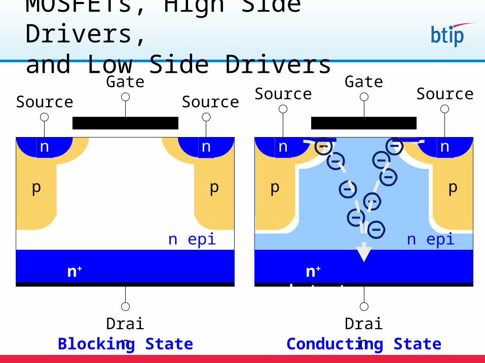
n n
GateSourceSource
n+ substrate
p p
n+ substrate
n
GateSourceSource
n+ substrate
p p
Drain DrainBlocking State Conducting State
n epi n epi
n
MOSFETs, High Side Drivers,and Low Side Drivers
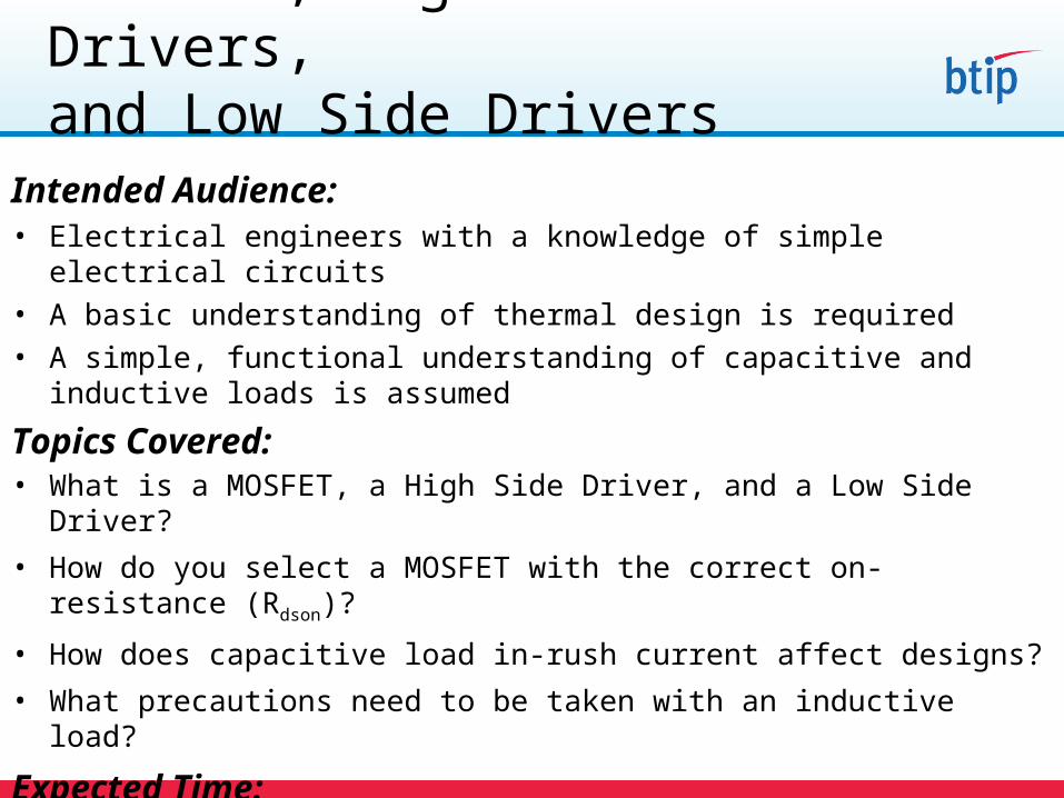
Intended Audience:• Electrical engineers with a knowledge of simple electrical circuits• A basic understanding of thermal design is required • A simple, functional understanding of capacitive and inductive loads is assumed
Topics Covered:• What is a MOSFET, a High Side Driver, and a Low Side Driver?
• How do you select a MOSFET with the correct on-resistance (Rdson)?
• How does capacitive load in-rush current affect designs?• What precautions need to be taken with an inductive load?
Expected Time:• Approximately 90 minutes
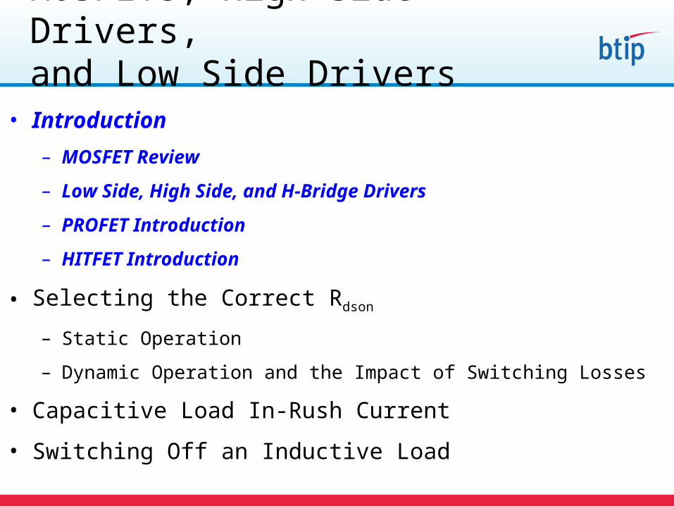
• Introduction
– MOSFET Review
– Low Side, High Side, and H-Bridge Drivers
– PROFET Introduction
– HITFET Introduction
• Selecting the Correct Rdson
– Static Operation
– Dynamic Operation and the Impact of Switching Losses
• Capacitive Load In-Rush Current
• Switching Off an Inductive Load
MOSFETs, High Side Drivers,and Low Side Drivers
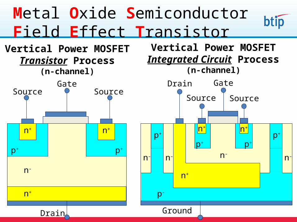
Metal Oxide SemiconductorField Effect Transistor
Gate
n+
p+
n+
p+
n+
n-
Source Source
Drain
Vertical Power MOSFETTransistor Process
(n-channel)
Vertical Power MOSFETIntegrated Circuit Process
(n-channel)
p-
n-
Drain
Ground
n+
Gate
p+
n- n-
p+
n-
p+ p+
Source Source
n+ n+
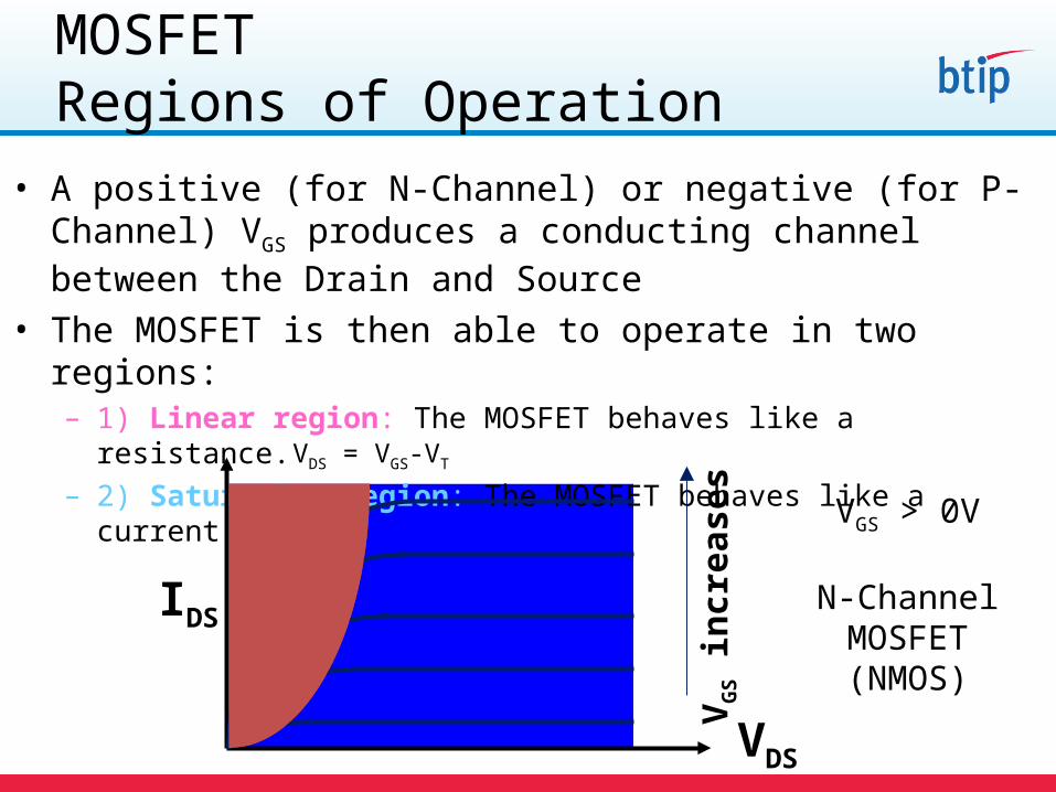
MOSFETRegions of Operation
• A positive (for N-Channel) or negative (for P-Channel) VGS produces a conducting channel between the Drain and Source
• The MOSFET is then able to operate in two regions:– 1) Linear region: The MOSFET behaves like a resistance.– 2) Saturation region: The MOSFET behaves like a current source.
VGS > 0V
N-ChannelMOSFET(NMOS)
IDS
VDS
VG
S i
ncr
ease
s
VDS = VGS-VT
MOSFET Breakdown• The breakdown voltage, V(BR)DSS, is the voltage at which current will
begin to flow from drain-source in OFF-state due to avalanche breakdown process
• For Drain-Source voltages above V(BR)DSS, significant current can flow through the MOSFET, even when it is turned off
V(BR)DSS
ID ElectricalCharacteristic
Drain-to-Source Breakdown Voltage
Symbol
V(BR)DSS
Condition
VGS = 0V
ID = 1mA
Minimum
25V
Drain
Source
Gate
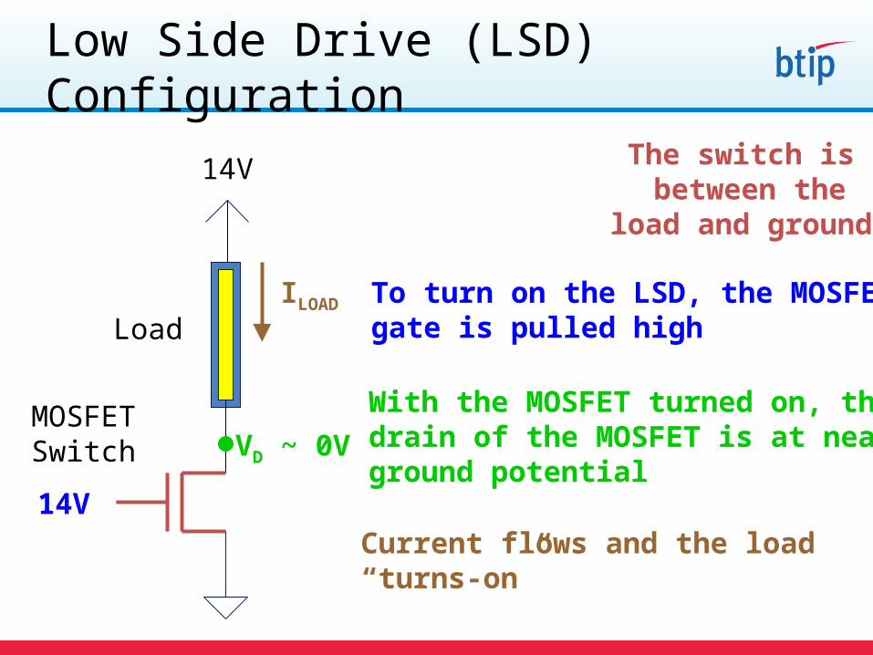
Low Side Drive (LSD) Configuration
The switch is between the
load and ground
14V
Load
MOSFETSwitch
To turn on the LSD, the MOSFETgate is pulled high
14V
With the MOSFET turned on, thedrain of the MOSFET is at nearground potential
VD ~ 0V
Current flows and the load “turns-on”
ILOAD
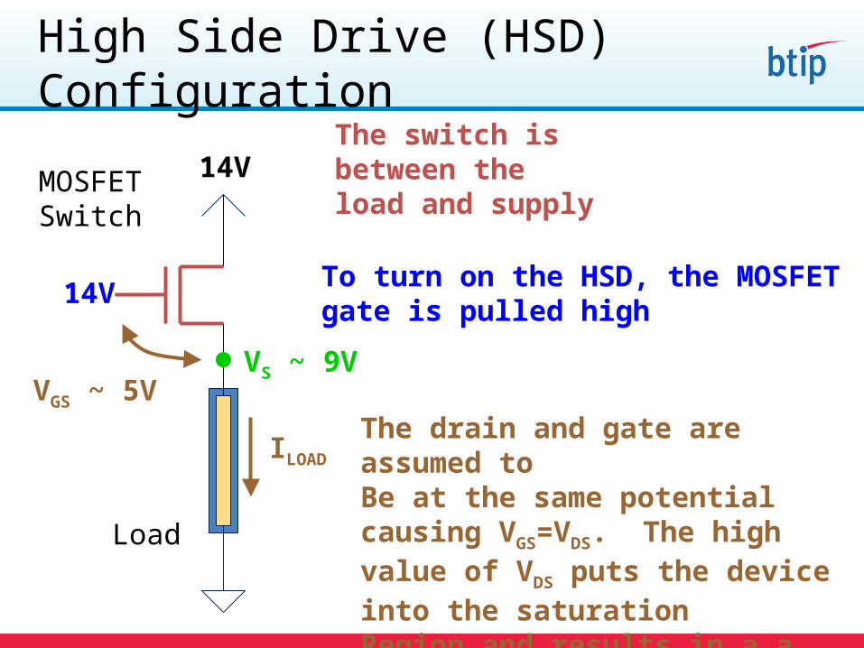
High Side Drive (HSD) Configuration
14V
Load
MOSFETSwitch
The switch isbetween theload and supply
To turn on the HSD, the MOSFETgate is pulled high
VS ~ 9V
The drain and gate are assumed toBe at the same potential causing VGS=VDS. The high value of VDS puts the device into the saturationRegion and results in a a small ILOAD.
ILOAD
VGS ~ 5V
14V
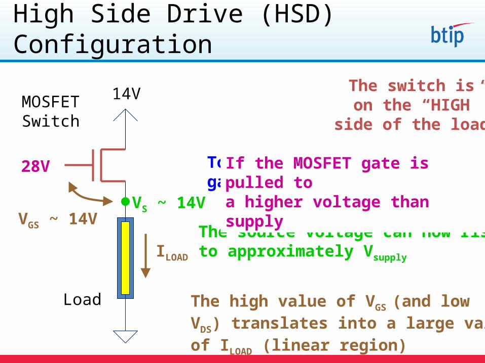
High Side Drive (HSD) Configuration
14V
Load
MOSFETSwitch
The switch is on the “HIGH”side of the load
To turn on the HSD, the MOSFETgate is pulled high
28V
The source voltage can now rise to approximately Vsupply
VS ~ 14V
If the MOSFET gate is pulled toa higher voltage than supply
The high value of VGS (and lowVDS) translates into a large valueof ILOAD (linear region)
ILOAD
VGS ~ 14V
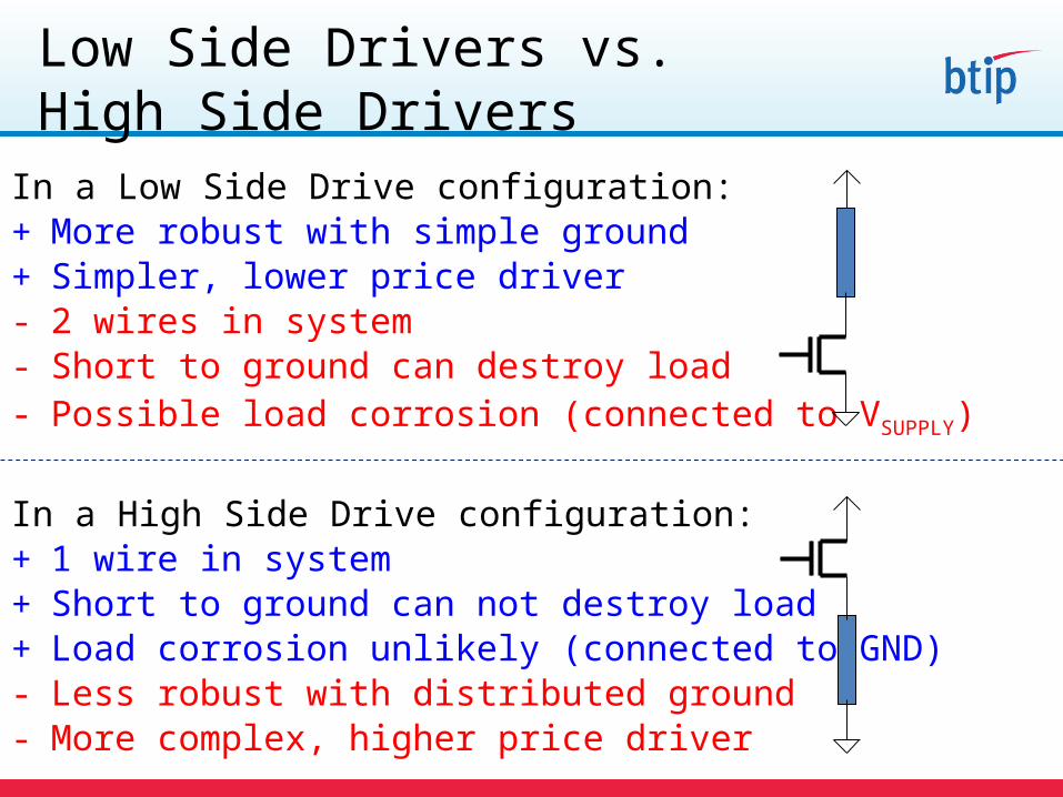
In a Low Side Drive configuration:+ More robust with simple ground+ Simpler, lower price driver- 2 wires in system- Short to ground can destroy load- Possible load corrosion (connected to VSUPPLY)
In a High Side Drive configuration:+ 1 wire in system+ Short to ground can not destroy load+ Load corrosion unlikely (connected to GND)- Less robust with distributed ground- More complex, higher price driver
Low Side Drivers vs.High Side Drivers
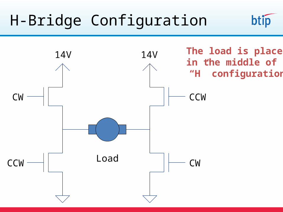
H-Bridge Configuration
14V 14V
Load
CW CCW
CCW CW
The load is placedin the middle of a“H” configuration
H-Bridge Configuration
14V 14V
Load
A CCW
CCW A
The load is placedin the middle of a“H” configuration
To turn the load onin one direction, “CW” is pulled high
28V
14V
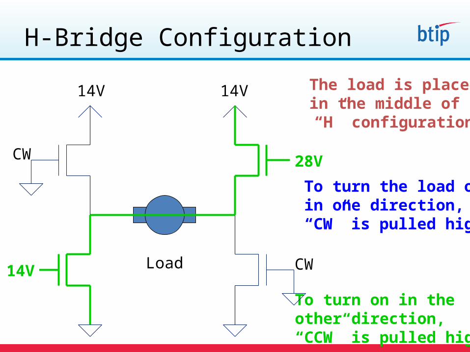
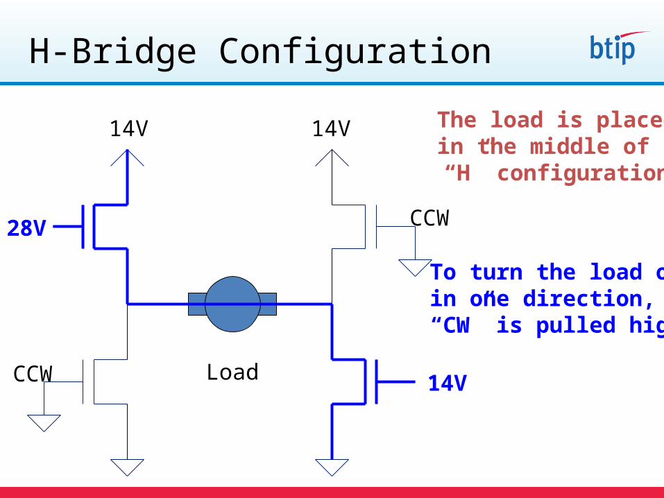
H-Bridge Configuration
14V 14V
Load
CW B
B CW
The load is placedin the middle of a“H” configuration
To turn the load onin one direction, “CW” is pulled high
To turn on in the other direction, “CCW” is pulled high
14V
28V
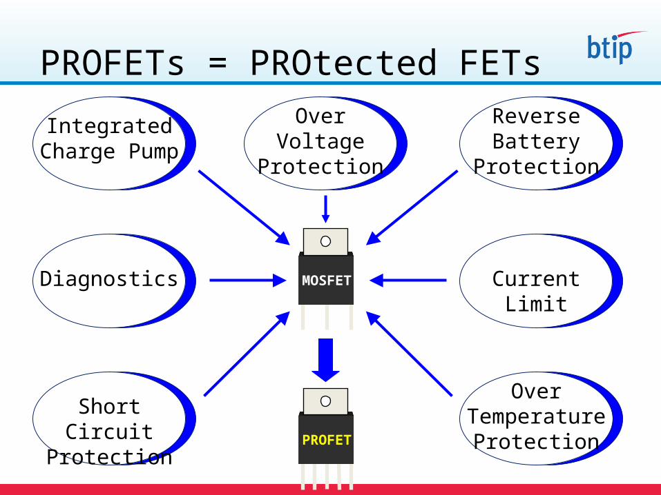
PROFETs = PROtected FETs
PROFET
MOSFETDiagnostics
Short CircuitProtection
IntegratedCharge Pump
OverVoltage
Protection
Current Limit
OverTemperature
Protection
ReverseBattery
Protection
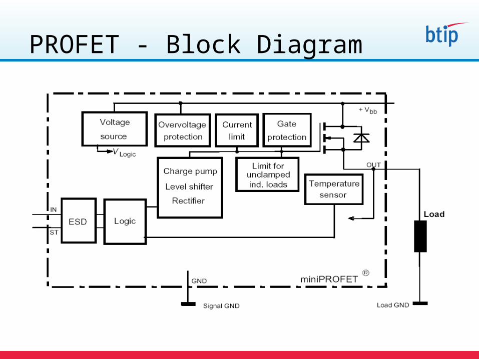
PROFET - Block Diagram
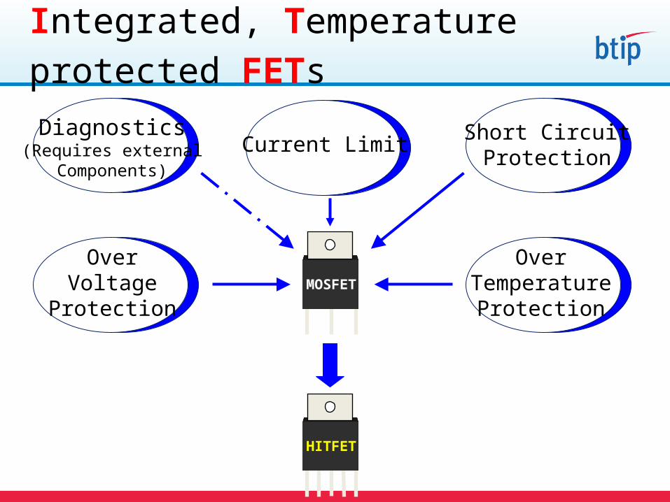
HITFETs =Highly Integrated, Temperature protected FETs
HITFET
MOSFET
Diagnostics(Requires external
Components)
OverVoltage
Protection
Current LimitShort CircuitProtection
OverTemperature
Protection
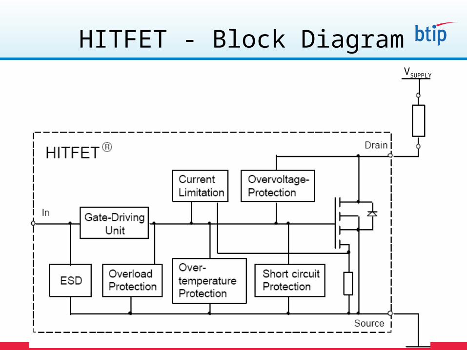
HITFET - Block DiagramVSUPPLY
• Introduction
– MOSFET Review
– Low Side, High Side, and H-Bridge Drivers
– PROFET Introduction
– HITFET Introduction
• Selecting the Correct Rdson
– Static Operation
– Dynamic Operation and the Impact of Switching Losses
• Capacitive Load In-Rush Current
• Switching Off an Inductive Load
MOSFETs, High Side Drivers,and Low Side Drivers
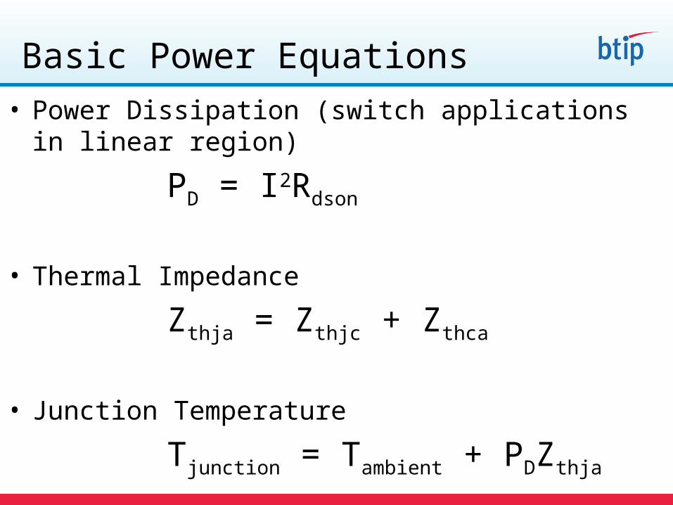
• Power Dissipation (switch applications in linear region)
PD = I2Rdson
• Thermal Impedance
Zthja = Zthjc + Zthca
• Junction Temperature
Tjunction = Tambient + PDZthja
• For static operation Zthja = Rthja
Basic Power Equations
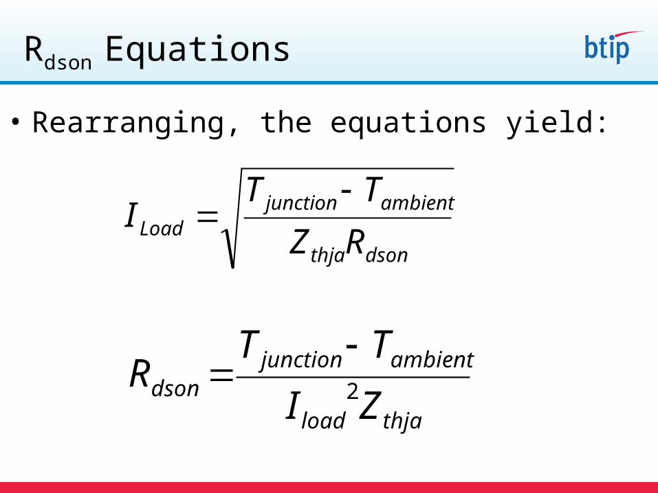
Rdson Equations
• Rearranging, the equations yield:
dsonthja
ambientjunctionLoad RZ
TTI
thjaload
ambientjunctiondson
ZI
TTR 2

Parameters Affecting Rdson Selection
• Typically, the following parameters are set by the device:Tjunction,max - Usually 150°C
Rdson - Function of the silicon die and package
Zthjc - Function of the package type (and die size)
• Typically, the following parameters are set by the application:
Tambient - Usually 85°C, 105°C, or 125°C
Iload - Function of the load resistance
Zthca - Function of the external heatsink

Datasheet Parameters Affecting Rdson Selection
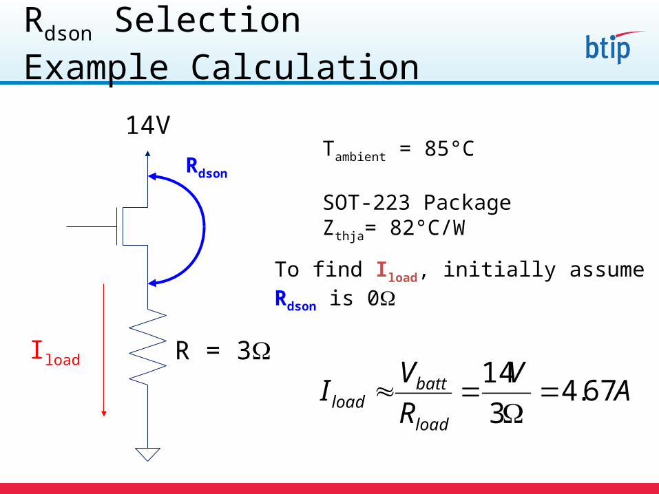
Rdson Selection Example Calculation
Tambient = 85°C
SOT-223 PackageZthja= 82°C/W
14V
R = 3Iload
To find Iload, initially assumeRdson is 0
Rdson
AV
R
VI
load
battload 67.4
3
14
Rdson Selection Example Calculation
14V
R = 3
junction,max ambientdson 2
load thja
T - TR
I Z
Rdson can now be calculated fordifferent Tjunction,max
( ) ( )m22=
W/C82A67.4
C85C125≤R 2dson
( ) ( )m36=
W/C82A67.4
C85C150≤R 2dson
Iload

82 C/W
SOT-223 Heatsink
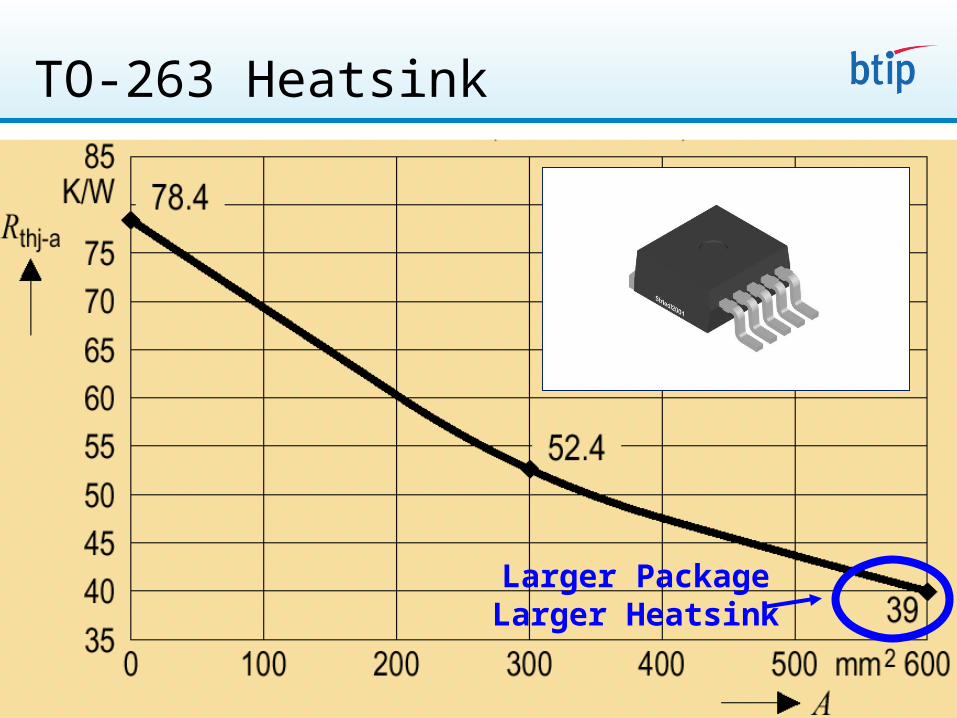
TO-263 Heatsink
Larger PackageLarger Heatsink
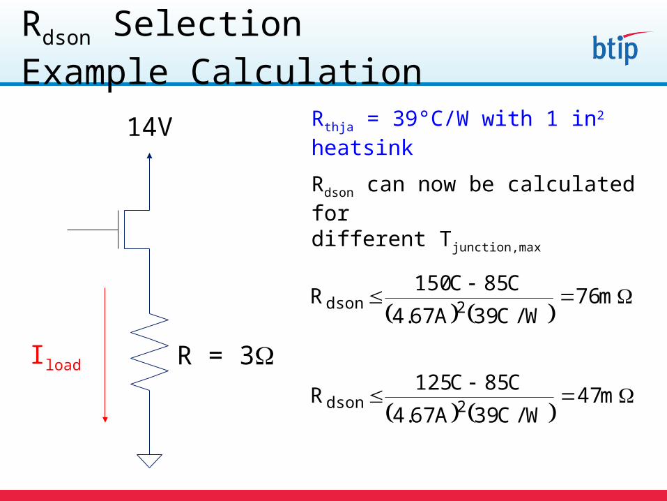
Rdson Selection Example Calculation
Rdson can now be calculated fordifferent Tjunction,max
m76
W/C39A67.4
C85C150R
2dson
m47
W/C39A67.4
C85C125R
2dson
Rthja = 39°C/W with 1 in2 heatsink14V
R = 3Iload
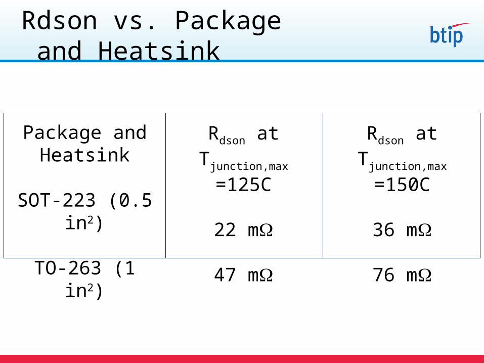
Rdson vs. Package and Heatsink
Package andHeatsink
SOT-223 (0.5 in2)
TO-263 (1 in2)
Rdson atTjunction,max =125C
22 m
47 m
Rdson atTjunction,max =150C
36 m
76 m
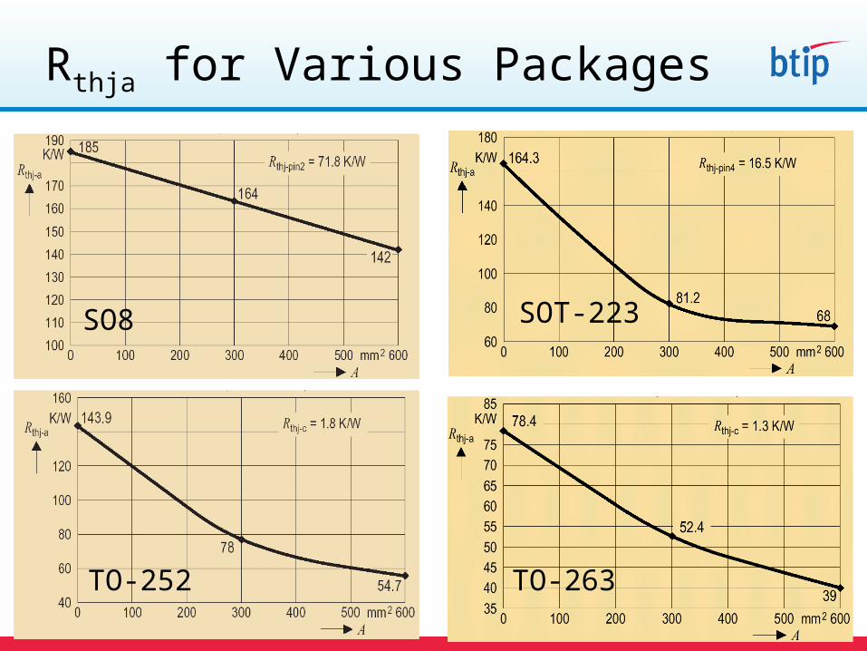
Rthja for Various Packages
SO8 SOT-223
TO-263TO-252
• Introduction
– MOSFET Review
– Low Side, High Side, and H-Bridge Drivers
– PROFET Introduction
– HITFET Introduction
• Selecting the Correct Rdson
– Static Operation
– Dynamic Operation and the Impact of Switching Losses
• Capacitive Load In-Rush Current
• Switching Off an Inductive Load
MOSFETs, High Side Drivers,and Low Side Drivers

Impact of Approximate FETSwitching Loss
0.0 0.2 0.4 0.6 0.8 1.0
1.0
0.8
0.6
0.4
0.2
0.0
Time All values normalized
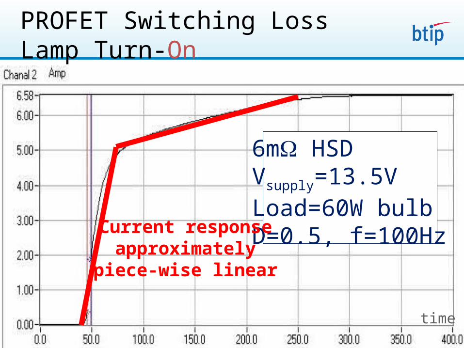
PROFET Switching LossLamp Turn-On
6m HSDVsupply=13.5VLoad=60W bulbD=0.5, f=100HzCurrent response
approximatelypiece-wise linear
time
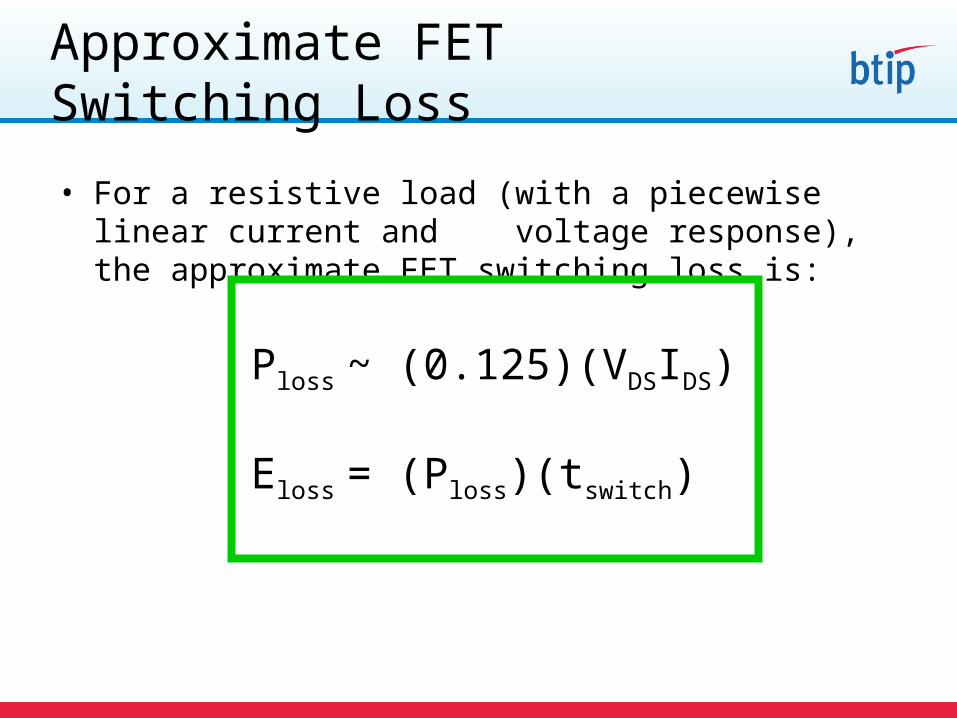
• For a resistive load (with a piecewise linear current and voltage response), the approximate FET switching loss is:
Approximate FETSwitching Loss
Ploss ~ (0.125)(VDSIDS)
Eloss = (Ploss)(tswitch)
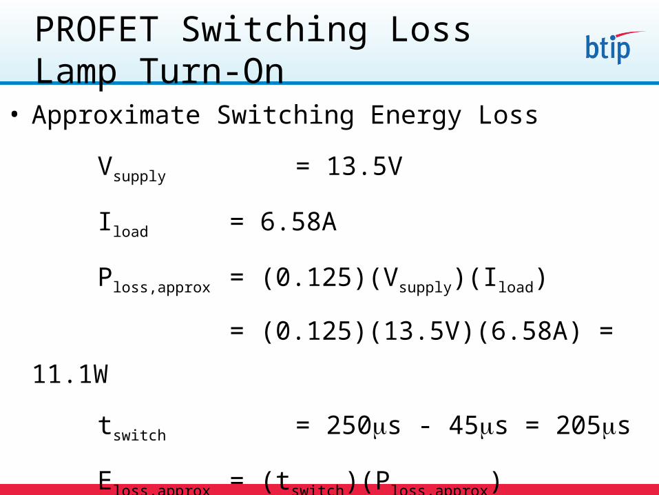
• Approximate Switching Energy Loss
Vsupply = 13.5V
Iload = 6.58A
Ploss,approx = (0.125)(Vsupply)(Iload)
= (0.125)(13.5V)(6.58A) = 11.1W
tswitch = 250s - 45s = 205s
Eloss,approx = (tswitch)(Ploss,approx)
= (205s)(11.1W) = 2.28mJ
PROFET Switching LossLamp Turn-On
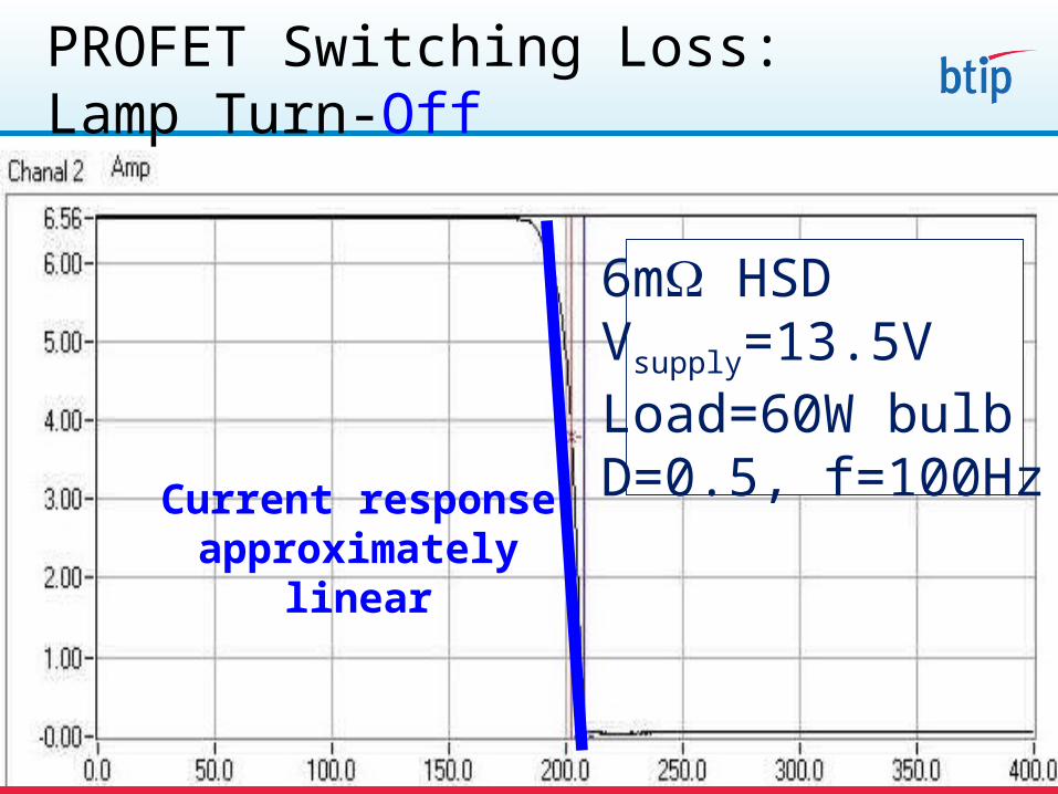
PROFET Switching Loss:Lamp Turn-Off
6m HSDVsupply=13.5VLoad=60W bulbD=0.5, f=100HzCurrent response
approximatelylinear
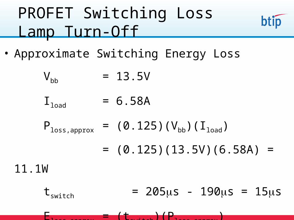
• Approximate Switching Energy Loss
Vbb = 13.5V
Iload = 6.58A
Ploss,approx = (0.125)(Vbb)(Iload)
= (0.125)(13.5V)(6.58A) = 11.1W
tswitch = 205s - 190s = 15s
Eloss,approx = (tswitch)(Ploss,approx)
= (15s)(11.1W) = 0.17mJ
PROFET Switching LossLamp Turn-Off
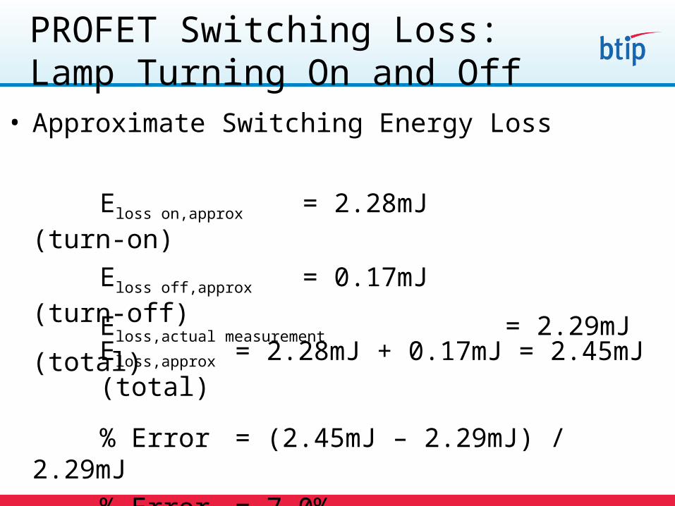
Eloss,actual measurement = 2.29mJ (total)
% Error = (2.45mJ – 2.29mJ) / 2.29mJ% Error = 7.0%
PROFET Switching Loss:Lamp Turning On and Off
• Approximate Switching Energy Loss
Eloss on,approx = 2.28mJ (turn-on)
Eloss off,approx = 0.17mJ (turn-off)
Eloss,approx = 2.28mJ + 0.17mJ = 2.45mJ (total)

Rdson Calculations for PWM Applications
• The power dissipated in a PWM application is given by:
PD = Pswitching + Pon
Pswitching = (Fswitching)(Ploss-ontturn-on + Ploss-offtturn-off)
Ploss-off (0.125)(VsupplyIload)
Ploss-on (0.125)(VsupplyIload)
Pon = (Iload2)(Rdson)(tpulse-on)(Fswitching)
Tjunction = Tambient + PDRthja
D = (tpulse-on)(Fswitching) = (tpulse-on) / (TPeriod)
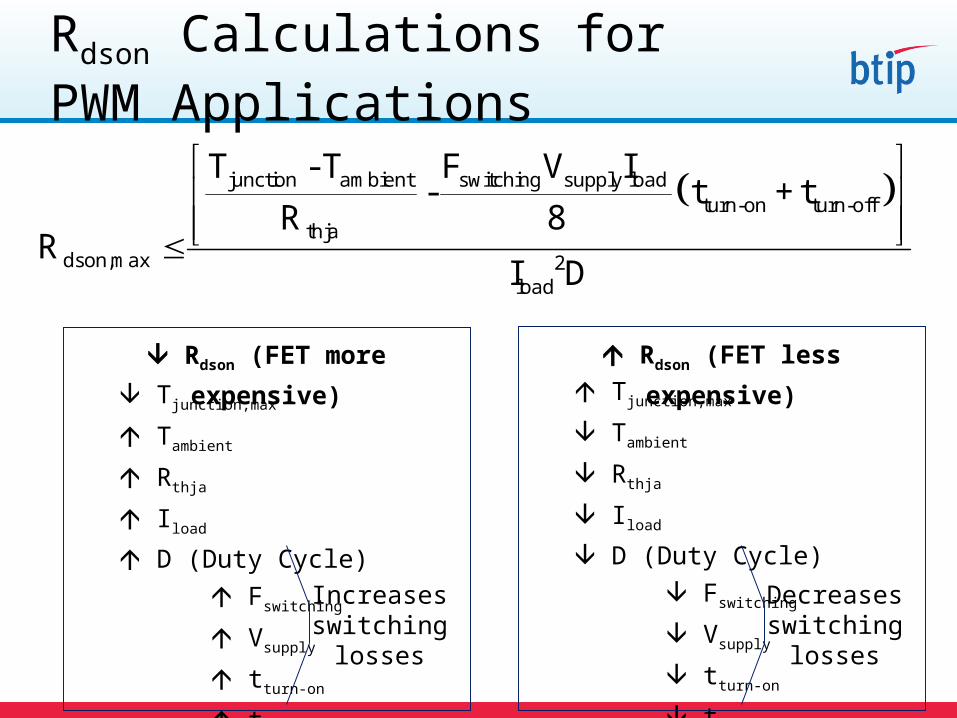
Tjunction,max
Tambient
Rthja
Iload
D (Duty Cycle)
Fswitching
Vsupply
tturn-on
tturn-off
Rdson (FET less expensive) Rdson (FET more expensive)
Decreasesswitching
losses
Tjunction,max
Tambient
Rthja
Iload
D (Duty Cycle)
Fswitching
Vsupply
tturn-on
tturn-off
Increasesswitching
losses
Rdson Calculations for PWM Applications
junction ambient switching supply loadturn-on turn-off
thja
dson,max 2load
T - T F V I- t + t
R 8R
I D
junction ambient switching supply loadturn-on turn-off
thja
dson 2load
T - T F V I- t + t
R 8R
I D
dson 2
100Hz 13.5V 6.57A150C-85C- 155μs+30μs
55K/W 8R
6.57A 0.5
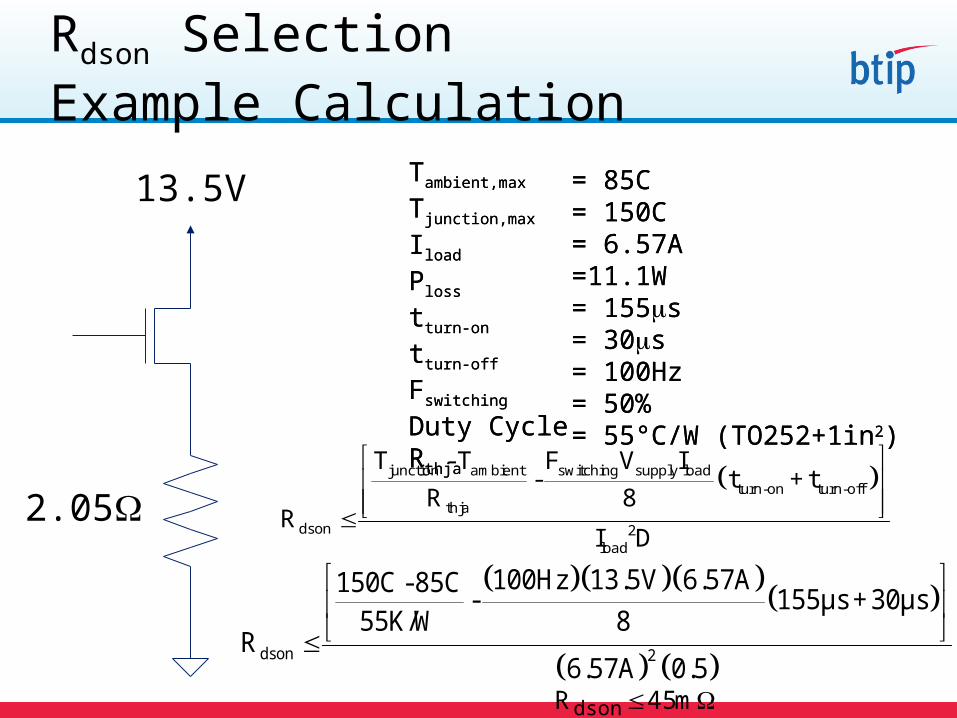
Rdson Selection Example Calculation
13.5V
2.05
Tambient,max
Tjunction,max
Iload
Ploss
tturn-on
tturn-off
Fswitching
Duty CycleRthja
= 85C= 150C= 6.57A=11.1W= 155s= 30s= 100Hz= 50%= 55°C/W (TO252+1in2)
m45Rdson
Tambient,max
Tjunction,max
Iload
Ploss
tturn-on
tturn-off
Fswitching
Duty CycleRthja
= 85C= 150C= 6.57A=11.1W= 155s= 30s= 100Hz= 50%= 55°C/W (TO252+1in2)
• Introduction
– MOSFET Review
– Low Side, High Side, and H-Bridge Drivers
– PROFET Introduction
– HITFET Introduction
• Selecting the Correct Rdson
– Static Operation
– Dynamic Operation and the Impact of Switching Losses
• Capacitive Load In-Rush Current
• Switching Off an Inductive Load
MOSFETs, High Side Drivers,and Low Side Drivers
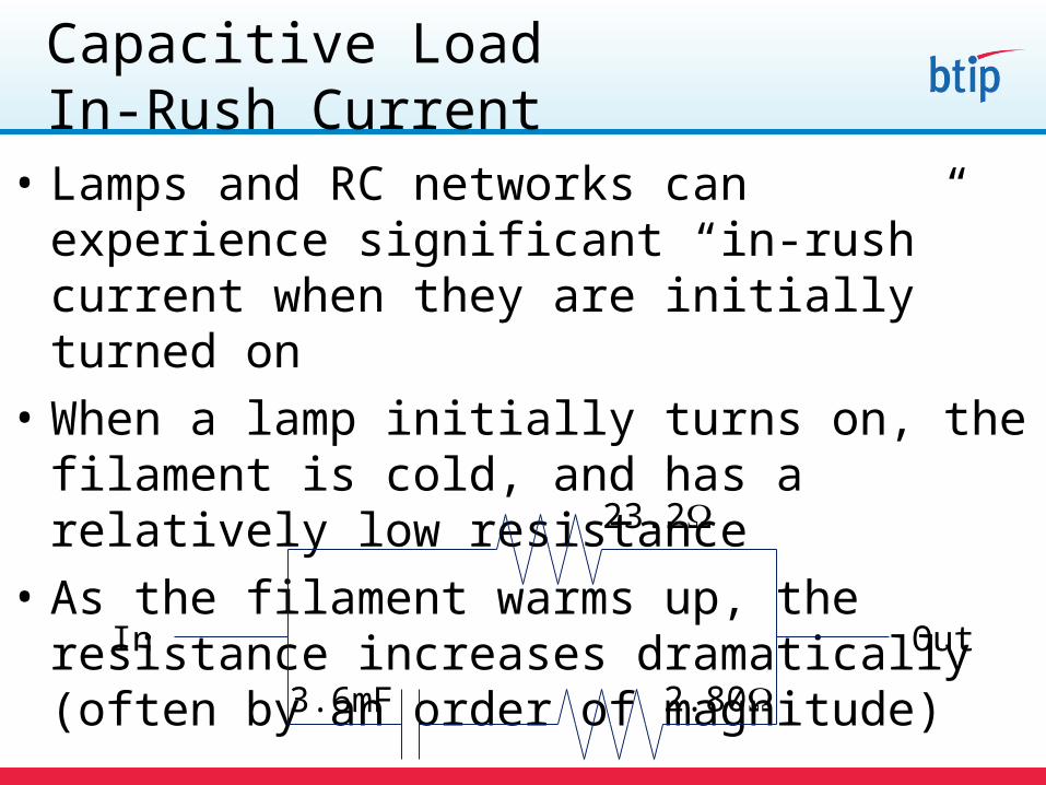
• Lamps and RC networks can experience significant “in-rush” current when they are initially turned on
• When a lamp initially turns on, the filament is cold, and has a relatively low resistance
• As the filament warms up, the resistance increases dramatically (often by an order of magnitude)
Capacitive LoadIn-Rush Current
In Out
23.2
2.803.6mF
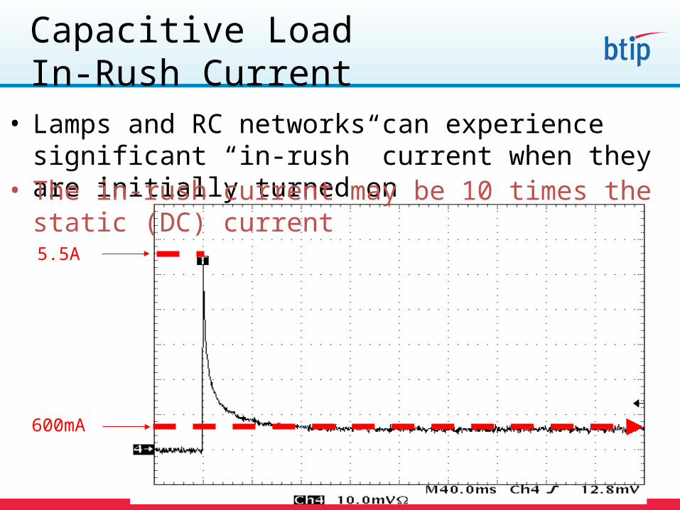
• Lamps and RC networks can experience significant “in-rush” current when they are initially turned on
Capacitive LoadIn-Rush Current
600mA
5.5A
• The in-rush current may be 10 times the static (DC) current

Standard Current Limiting• When the load resistance is lower than expected, PROFETs/HITFETs can
go into a protective current limiting mode
• Current limiting is considered a FAULT condition – devices are not designed for prolonged use in this mode of operation
• Care must be taken to keep in-rush current levels below the device’s current limit threshold
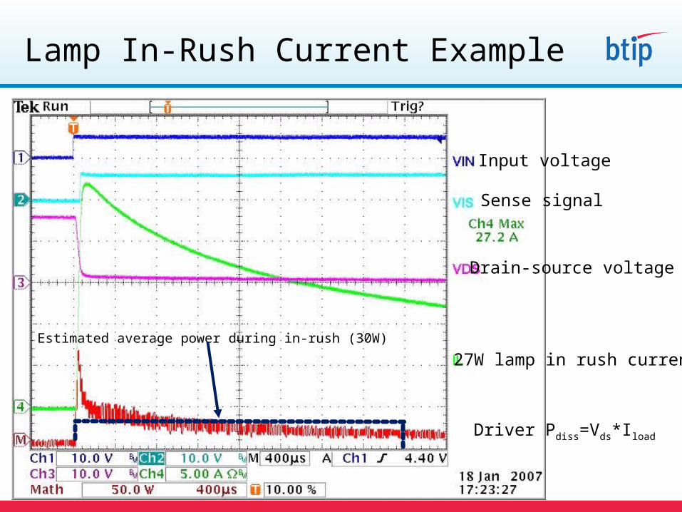
Lamp In-Rush Current Example
Input voltage
Sense signal
Drain-source voltage
27W lamp in rush current
Driver Pdiss=Vds*Iload
Estimated average power during in-rush (30W)

0.01
0.1
1
10
100
1E-6 1E-5 1E-4 1E-3 1E-2 1E-1 1E0 1E1 1E2 1E3 1E4
tp [s]
Z th
JA [
K/W
]
00,01
0,020,050,10,20,5D=
Zthja Chart for LampIn-Rush Current Example
Single Pulse
2.0°C/W
~3msec
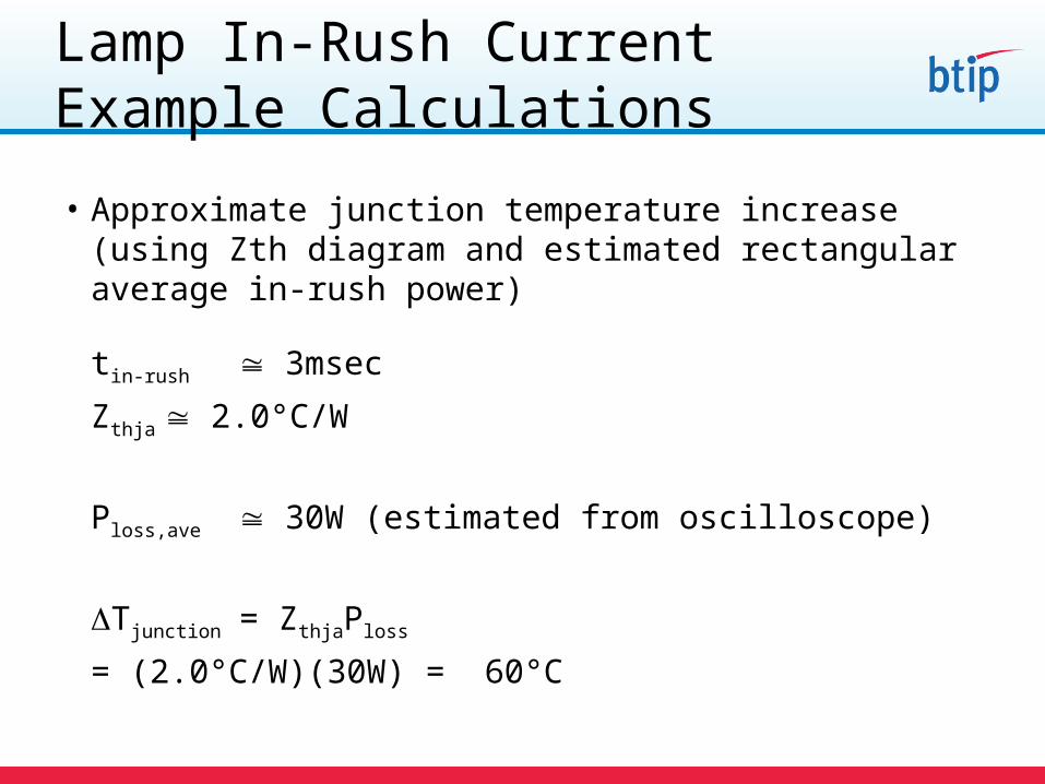
• Approximate junction temperature increase (using Zth diagram and estimated rectangular average in-rush power)
tin-rush 3msec
Zthja 2.0°C/W
Ploss,ave 30W (estimated from oscilloscope)
Tjunction = ZthjaPloss
= (2.0°C/W)(30W) = 60°C
Lamp In-Rush CurrentExample Calculations

• Introduction
– MOSFET Review
– Low Side, High Side, and H-Bridge Drivers
– PROFET Introduction
– HITFET Introduction
• Selecting the Correct Rdson
– Static Operation
– Dynamic Operation and the Impact of Switching Losses
• Capacitive Load In-Rush Current
• Switching Off an Inductive Load
MOSFETs, High Side Drivers,and Low Side Drivers
Switching OFF anInductive Load
OFF
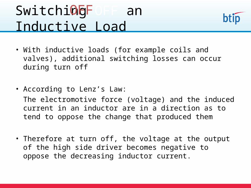
• With inductive loads (for example coils and valves), additional switching losses can occur during turn off
• According to Lenz’s Law:The electromotive force (voltage) and the induced current in an inductor are in a direction as to tend to oppose the change that produced them
• Therefore at turn off, the voltage at the output of the high side driver becomes negative to oppose the decreasing inductor current.
Switching OFF an Inductive Load
VOUT
Vbb
VINVON
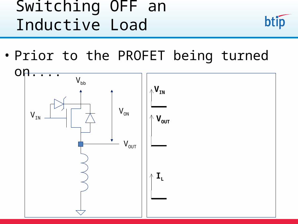
• Prior to the PROFET being turned on....
IL
VIN
VOUT
IL
Switching OFF an Inductive Load
VOUT
Vbb
VINVON
IL
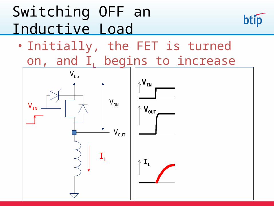
• Initially, the FET is turned on, and IL begins to increase
IL
VIN
VOUT
IL
VOUT
Vbb
VINVON
HIGH
IL
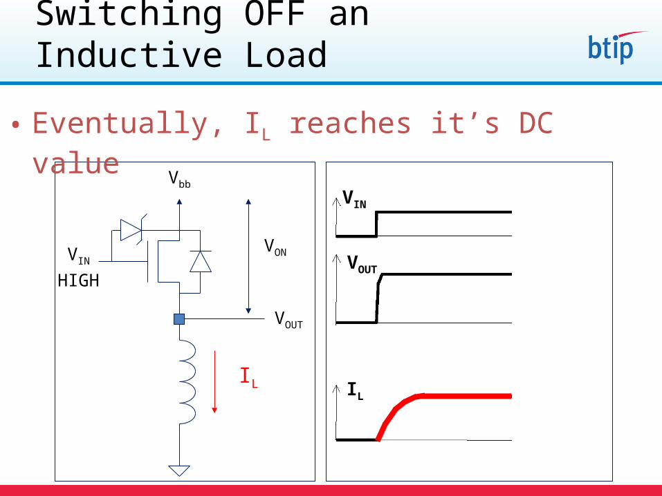
• Eventually, IL reaches it’s DC value
Switching OFF an Inductive Load
IL
VIN
VOUT
IL
VOUT
Vbb
VINVON
IL
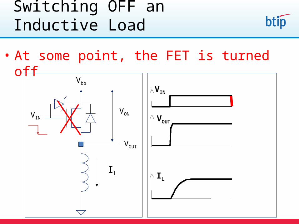
• At some point, the FET is turned off
Switching OFF an Inductive Load
IL
VIN
VOUT
IL
VOUT
Vbb
VINVON
VON(CL)
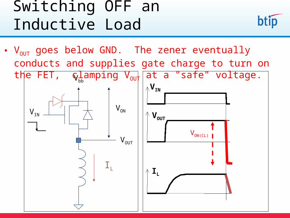
• VOUT goes below GND. The zener eventually conducts and supplies gate charge to turn on the FET, clamping VOUT at a "safe" voltage.
Switching OFF an Inductive Load
IL
VIN
VOUT
IL
IL
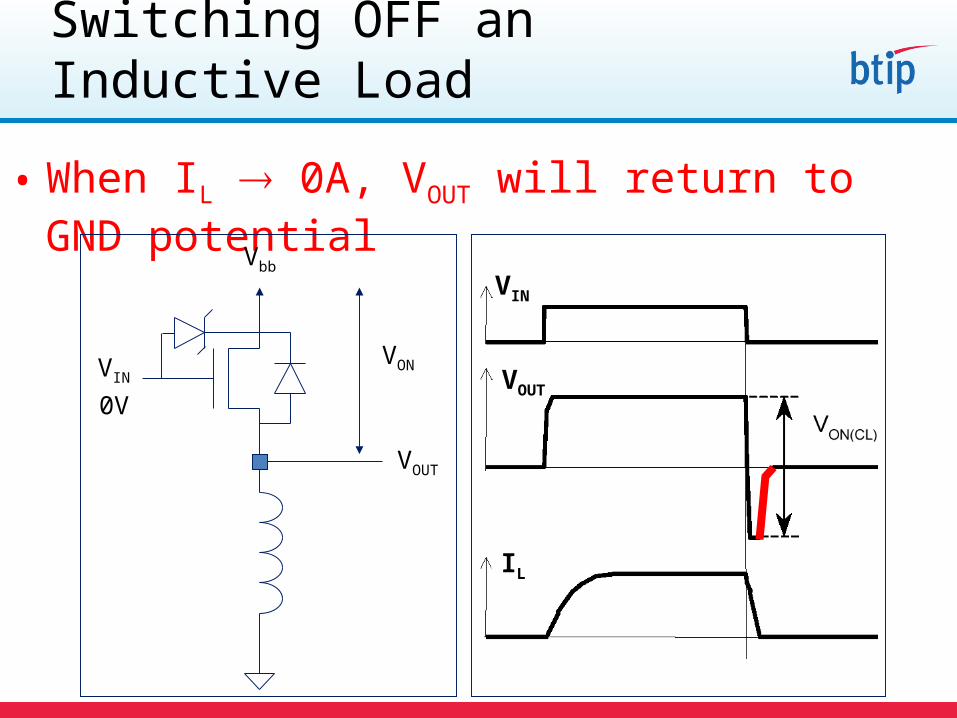
• When IL 0A, VOUT will return to GND potential
Switching OFF an Inductive Load
VOUT
Vbb
VINVON
0V
IL
VIN
VOUT
IL
Safely Clamping VOUT for Inductive Loads
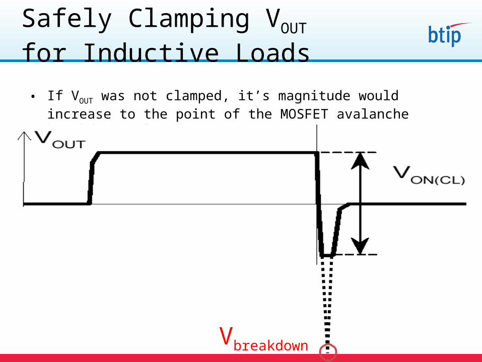
• If VOUT was not clamped, it’s magnitude would increase to the point of the MOSFET avalanche breakdown voltage
Vbreakdown
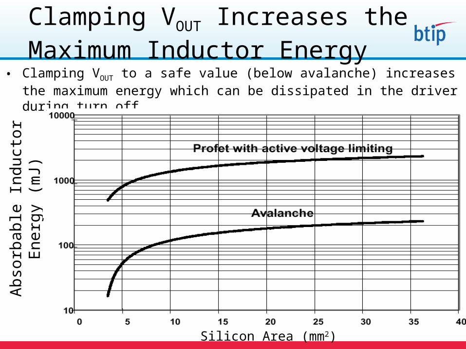
• Clamping VOUT to a safe value (below avalanche) increases the maximum energy which can be dissipated in the driver during turn off
Silicon Area (mm2)
Abs
orba
ble
Indu
ctor
Ene
rgy
(mJ)
Clamping VOUT Increases the Maximum Inductor Energy

• The maximum safe inductive energy which can be dissipated in the FET is found in the maximum ratings section:
• The clamping voltage is in the electrical characteristics:
Maximum Safe Inductor Energy
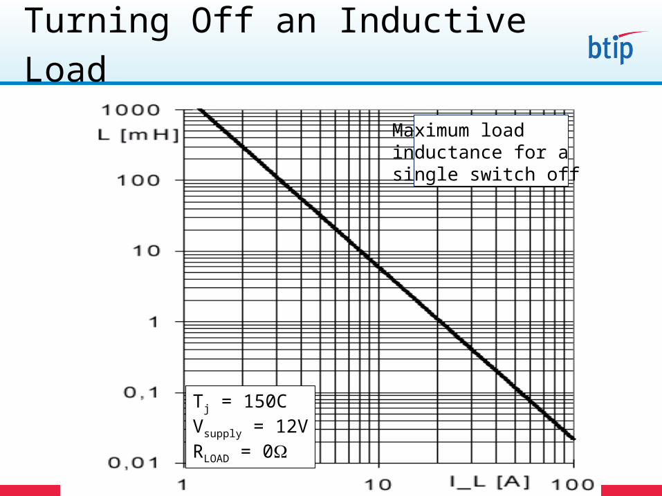
Energy Absorbed When Turning Off an Inductive Load
Tj = 150CVsupply = 12VRLOAD = 0
Maximum loadinductance for asingle switch off
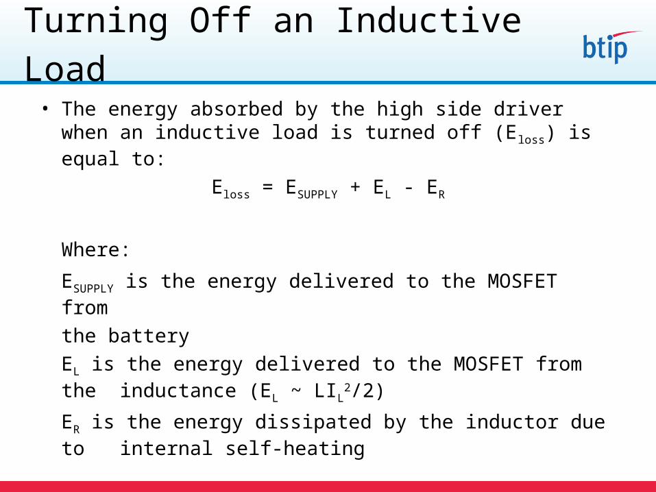
• The energy absorbed by the high side driver when an inductive load is turned off (Eloss) is equal to:
Eloss = ESUPPLY + EL - ER
Where:
ESUPPLY is the energy delivered to the MOSFET from
the batteryEL is the energy delivered to the MOSFET from the
inductance (EL ~ LIL2/2)
ER is the energy dissipated by the inductor due to internal self-heating
Energy Absorbed When Turning Off an Inductive Load
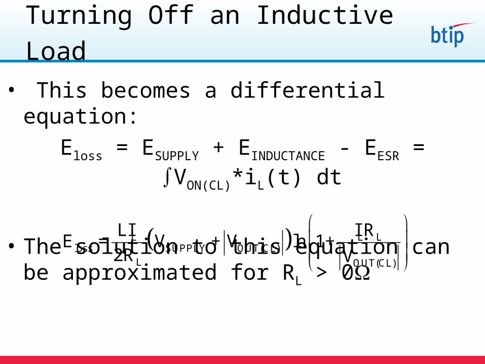
• This becomes a differential equation:Eloss = ESUPPLY + EINDUCTANCE - EESR = ∫VON(CL)*iL(t) dt
• The solution to this equation can be approximated for RL > 0
Energy Absorbed When Turning Off an Inductive Load
L L Lloss SUPPLY OUT(CL)
L OUT(CL)
LI I RE = V + V ln 1+
2R V
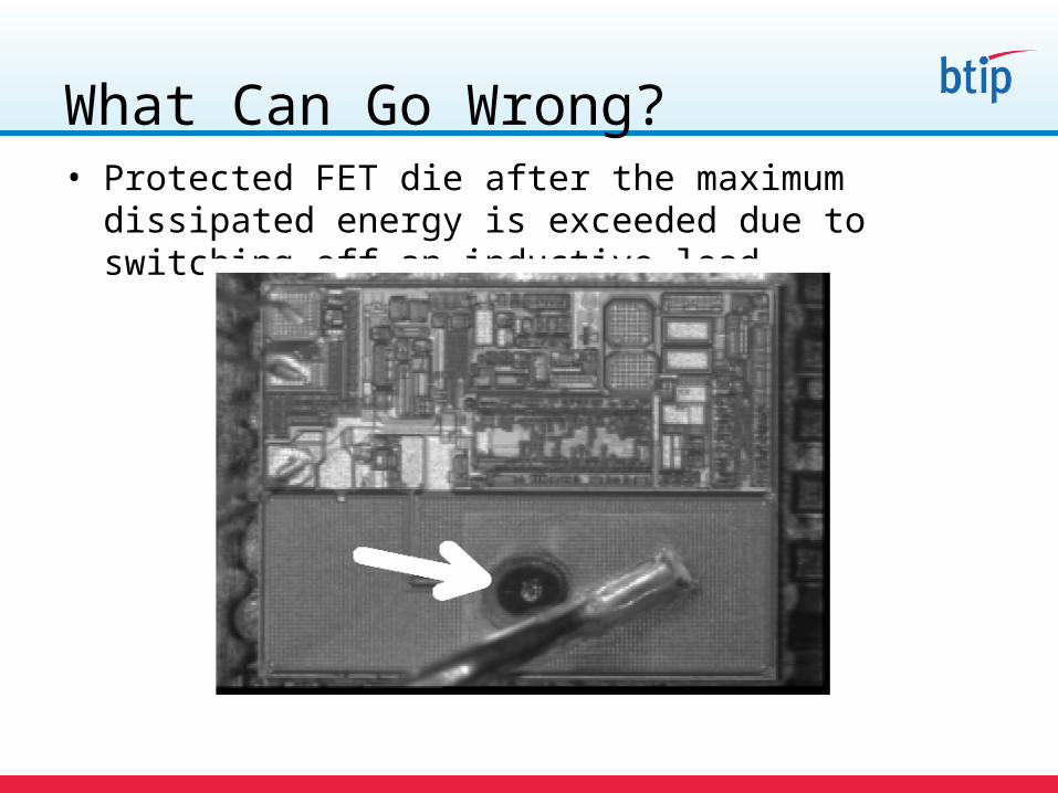
What Can Go Wrong? • Protected FET die after the maximum dissipated energy is
exceeded due to switching off an inductive load

Driving a FET with a PWM Input14V
Load
n+
p+
n+
p+
n+
n-
GateSource Source
Drain
Note: Generally, inductive loads are not PWM drivendue to the repetitiveclamping energy / power.
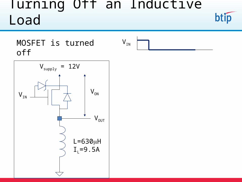
Turning Off an Inductive LoadVINMOSFET is turned off
VOUT
Vsupply = 12V
VINVON
L=630HIL=9.5A
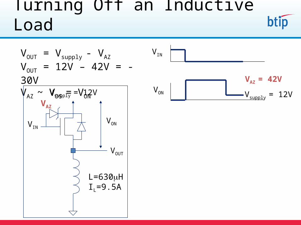
Vsupply = 12V
VAZ = 42V
VINVOUT = Vsupply - VAZ
VOUT = 12V – 42V = -30VVAZ ~ VDS = VON
Turning Off an Inductive Load
VOUT
Vsupply = 12V
VIN
L=630HIL=9.5A
VAZ
VON
VON
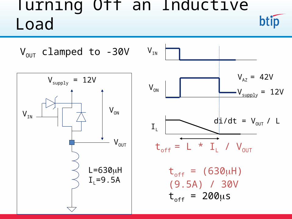
IL
di/dt = VOUT / L
toff = L * IL / VOUT
VIN
toff = (630H)(9.5A) / 30Vtoff = 200s
VOUT
Vsupply = 12V
VINVON
L=630HIL=9.5A
VON Vsupply = 12V
VAZ = 42V
Turning Off an Inductive Load
VOUT clamped to -30V
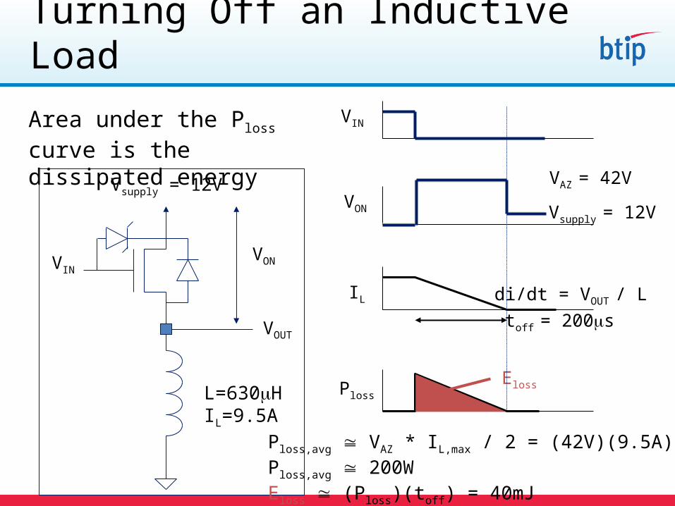
Ploss
Eloss
IL di/dt = VOUT / L
toff = 200s
VINArea under the Ploss curve is the dissipated energy
VOUT
Vsupply = 12V
VINVON
L=630HIL=9.5A
VON Vsupply = 12V
VAZ = 42V
Ploss,avg VAZ * IL,max / 2 = (42V)(9.5A) / 2Ploss,avg 200W Eloss (Ploss)(toff) = 40mJ
Turning Off an Inductive Load
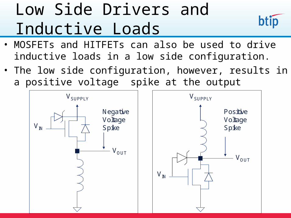
Low Side Drivers andInductive Loads
• MOSFETs and HITFETs can also be used to drive inductive loads in a low side configuration.
• The low side configuration, however, results in a positive voltage spike at the output
VOUT
VSUPPLY
VIN
VOUT
VSUPPLY
VIN
NegativeVoltageSpike
PositiveVoltageSpike
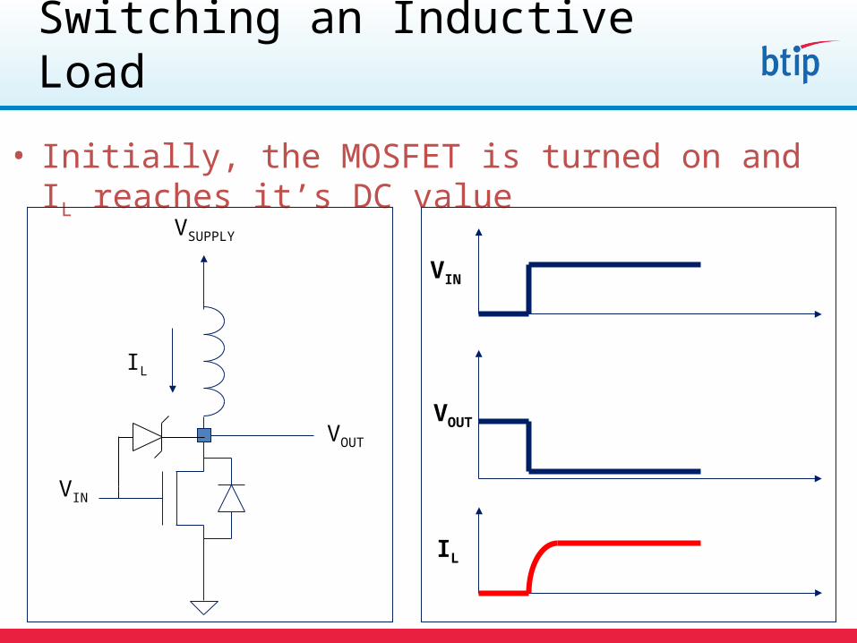
Switching an Inductive Load
• Initially, the MOSFET is turned on and IL reaches it’s DC value
VOUT
VSUPPLY
VIN
IL
VIN
IL
VOUT
IL
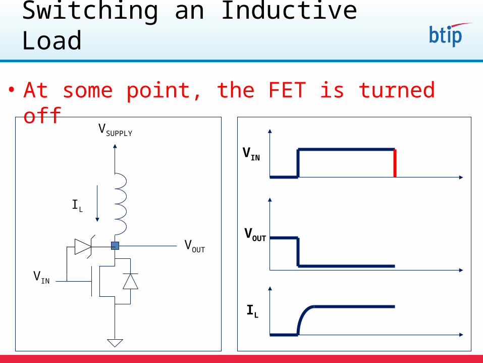
Switching an Inductive Load
• At some point, the FET is turned off
VOUT
VSUPPLY
VIN
IL
VIN
IL
VOUT
IL
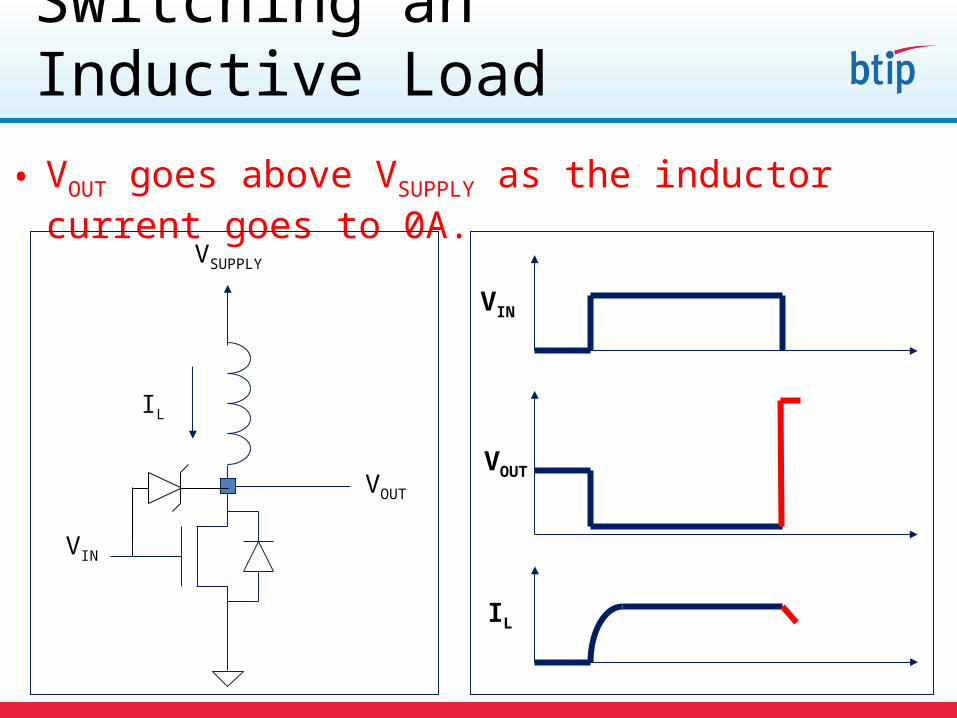
Switching an Inductive Load• VOUT goes above VSUPPLY as the inductor current goes to 0A.
VOUT
VSUPPLY
VIN
IL
VIN
IL
VOUT
IL
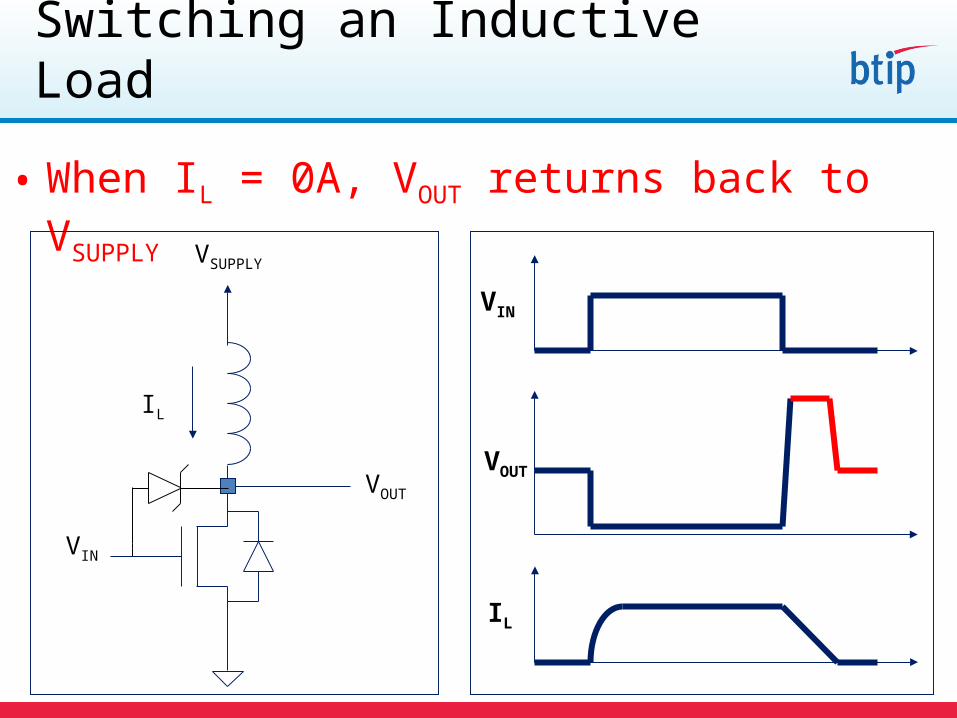
Switching an Inductive Load
• When IL = 0A, VOUT returns back to VSUPPLY
VOUT
VSUPPLY
VIN
IL
VIN
IL
VOUT
IL
• Introduction
– MOSFET Review
– Low Side, High Side, and H-Bridge Drivers
– PROFET Introduction
– HITFET Introduction
• Selecting the Correct Rdson
– Static Operation
– Dynamic Operation and the Impact of Switching Losses
• Capacitive Load In-Rush Current
• Switching Off an Inductive Load
MOSFETs, High Side Drivers,and Low Side Drivers
MOSFETs, High Side Drivers,and Low Side Drivers
n n
GateSourceSource
n+ substrate
p p
n+ substrate
n
GateSourceSource
n+ substrate
p p
Drain DrainBlocking State Conducting State
n epi n epi
n

Thank You!www.btipnow.com