CGHV27030, 30W, 20-6000MHz, GaN HEMT by Cree … · 4 CGHV27030S Rev 4.1 Cree, Inc 00 Silicon rie...
28
1 Subject to change without notice. www.cree.com/RF CGHV27030S 30 W, DC - 6.0 GHz, GaN HEMT The CGHV27030S is an unmatched, gallium nitride (GaN) high electron mobility transistor (HEMT) which offers high efficiency, high gain and wide bandwidth capabilities. The CGHV27030S GaN HEMT devices are ideal for telecommunications applications with frequencies of 700-960 MHz, 1200-1400 MHz, 1800-2200 MHz, 2500-2700 MHz, and 3300-3700 MHz at both 50 V and 28 V operations. The CGHV27030S is also ideal for tactical communications applications operating from 20-2500 MHz, including land mobile radios. Additional applications include L-Band RADAR and S-Band RADAR. The CGHV27030S can operate with either a 50 V or 28 V rail. The transistor is available in a 3mm x 4mm, surface mount, dual-flat-no-lead (DFN) package. Rev 4.1 – May 2017 Features for 50 V in CGHV27030S-AMP1 • 2.5 - 2.7 GHz Operation • 30 W Typical Output Power • 20 dB Gain at 5 W P AVE • -34 dBc ACLR at 5 W P AVE • 30% efficiency at 5 W P AVE • High degree of APD and DPD correction can be applied Typical Performance 2.5-2.7 GHz (T C = 25˚C) , 50 V Parameter 2.5 GHz 2.6 GHz 2.7 GHz Units Small Signal Gain 22.5 22.0 21.4 dB Adjacent Channel Power @ P OUT =5 W -34.5 -35.0 -34.0 dBc Drain Efficiency @ P OUT = 5 W 28.5 29.5 30.0 % Input Return Loss 8.5 14 14 dB Note: Measured in the CGHV27030S-AMP1 application circuit, under 7.5 dB PAR single carrier WCDMA signal test model 1 with 64 DPCH. Listing of Available Hardware Application Circuits / Demonstration Circuits Application Circuit Operating Frequency Amplifier Class Operating Voltage CGHV27030S-AMP1 2.5 - 2.7 GHz Class A/B 50 V CGHV27030S-AMP2 2.5 - 2.7 GHz Class A/B 28 V CGHV27030S-AMP3 1.8 - 2.2 GHz Class A/B 28 V CGHV27030S-AMP4 1.8 - 2.2 GHz Class A/B 50 V CGHV27030S-AMP5 1.2 - 1.4 GHz Class A/B 50 V Package Type: 3x4 DFN PN: CGHV27030S
Transcript of CGHV27030, 30W, 20-6000MHz, GaN HEMT by Cree … · 4 CGHV27030S Rev 4.1 Cree, Inc 00 Silicon rie...

1Subject to change without noticewwwcreecomRF
CGHV27030S30 W DC - 60 GHz GaN HEMT
The CGHV27030S is an unmatched gallium nitride (GaN) high electron mobility transistor (HEMT)
which offers high efficiency high gain and wide bandwidth capabilities The CGHV27030S GaN
HEMT devices are ideal for telecommunications applications with frequencies of 700-960
MHz 1200-1400 MHz 1800-2200 MHz 2500-2700 MHz and 3300-3700 MHz at both 50 V
and 28 V operations The CGHV27030S is also ideal for tactical communications applications
operating from 20-2500 MHz including land mobile radios Additional applications include L-Band
RADAR and S-Band RADAR The CGHV27030S can operate with either a 50 V or 28 V rail The transistor is available in a
3mm x 4mm surface mount dual-flat-no-lead (DFN) package
Rev
41
ndash M
ay 2
017
Features for 50 V in CGHV27030S-AMP1
bull 25 - 27 GHz Operationbull 30 W Typical Output Powerbull 20 dB Gain at 5 W PAVE
bull -34 dBc ACLR at 5 W PAVE
bull 30 efficiency at 5 W PAVE bull High degree of APD and DPD correction can be applied
Typical Performance 25-27 GHz (TC = 25˚C) 50 V
Parameter 25 GHz 26 GHz 27 GHz Units
Small Signal Gain 225 220 214 dB
Adjacent Channel Power POUT =5 W -345 -350 -340 dBc
Drain Efficiency POUT = 5 W 285 295 300
Input Return Loss 85 14 14 dB
NoteMeasured in the CGHV27030S-AMP1 application circuit under 75 dB PAR single carrier WCDMA signal test model 1 with 64 DPCH
Listing of Available Hardware Application Circuits Demonstration Circuits
Application Circuit Operating Frequency Amplifier Class Operating Voltage
CGHV27030S-AMP1 25 - 27 GHz Class AB 50 V
CGHV27030S-AMP2 25 - 27 GHz Class AB 28 V
CGHV27030S-AMP3 18 - 22 GHz Class AB 28 V
CGHV27030S-AMP4 18 - 22 GHz Class AB 50 V
CGHV27030S-AMP5 12 - 14 GHz Class AB 50 V
Package Type 3x4 DFNPN CGHV27030S
2 CGHV27030S Rev 41
Cree Inc4600 Silicon Drive
Durham North Carolina USA 27703USA Tel +19193135300
Fax +19198692733wwwcreecomrf
Copyright copy 2013 - 2017 Cree Inc All rights reserved The information in this document is subject to change without notice Cree and the Cree logo are registered trademarks of Cree Inc
Absolute Maximum Ratings (not simultaneous) at 25˚C Case Temperature
Parameter Symbol Rating Units Notes
Drain-Source Voltage VDSS 125 Volts 25˚C
Gate-to-Source Voltage VGS -10 +2 Volts 25˚C
Storage Temperature TSTG -65 +150 ˚C
Operating Junction Temperature TJ 225 ˚C
Maximum Forward Gate Current IGMAX 4 mA 25˚C
Maximum Drain Current1 IDMAX 15 A 25˚C
Soldering Temperature2 TS 245 ˚C
Case Operating Temperature3 TC -40 +150 ˚C
Thermal Resistance Junction to Case4 RθJC 618 ˚CW 85˚C
Note1 Current limit for long term reliable operation2 Refer to the Application Note on soldering at wwwcreecomrfdocument-library3 TC = Case temperature for the device It refers to the temperature at the ground tab underneath the package The PCB will add additional thermal resistance See also the Power Dissipation De-rating Curve on page 234 Measured for the CGHV27030S at PDISS = 12 W5 The RTH for Creersquos demonstration amplifier CGHV27030S-AMP1 with 33 x 0011 via holes designed on a 20 mil thick Rogers 4350 PCB is 39degC The total RTH from the heat sink to the junction is 618degC + 39degC = 1008degCW
Electrical Characteristics (TC = 25˚C)
Characteristics Symbol Min Typ Max Units Conditions
DC Characteristics1
Gate Threshold Voltage VGS(th) -38 -30 -23 VDC VDS = 10 V ID = 4 mA
Gate Quiescent Voltage VGS(Q) ndash -27 ndash VDC VDS = 50 V ID = 013 mA
Saturated Drain Current IDS 30 36 ndash A VDS = 60 V VGS = 20 V
Drain-Source Breakdown Voltage V(BR)DSS 150 ndash ndash VDC VGS = -8 V ID = 4 mA
RF Characteristics23 (TC = 25˚C F0 = 265 GHz unless otherwise noted)
Gain G 19 213 - dB VDD = 50 V IDQ = 013 A PIN = 10 dBm
Output Power4 POUT 43 44 ndash dBm VDD = 50 V IDQ = 013 A PIN = 28 dBm
Drain Efficiency4 η 48 60 - VDD = 50 V IDQ = 013 A PIN = 28 dBm
Output Mismatch Stress4 VSWR - 10 1 - Y No damage at all phase angles VDD = 50 V IDQ = 013 A PIN = 28 dBm
Dynamic Characteristics
Input Capacitance5 CGS ndash 538 ndash pF VDS = 50 V Vgs = -8 V f = 1 MHz
Output Capacitance5 CDS ndash 118 ndash pF VDS = 50 V Vgs = -8 V f = 1 MHz
Feedback Capacitance CGD ndash 012 ndash pF VDS = 50 V Vgs = -8 V f = 1 MHz
Notes1 Measured on wafer prior to packaging2 Scaled from PCM data3 Measured in Creersquos production test fixture This fixture is designed for high volume test at 265 GHz 4 Un-modulated Pulsed Signal 100 μs 10 duty cycle 5 Includes package parasitics
3 CGHV27030S Rev 41
Cree Inc4600 Silicon Drive
Durham North Carolina USA 27703USA Tel +19193135300
Fax +19198692733wwwcreecomrf
Copyright copy 2013 - 2017 Cree Inc All rights reserved The information in this document is subject to change without notice Cree and the Cree logo are registered trademarks of Cree Inc
Typical Performance in Application Circuit CGHV27030S-AMP1
Figure 1 - Small Signal Gain and Return Losses vs Frequency VDD = 50 V IDQ = 013 A
Figure 2 - Typical Drain Efficiency and ACLR vs Output Power VDD = 50 V IDQ = 013 A 1c WCDMA PAR = 75 dB
Efficiency
ACLR
4 CGHV27030S Rev 41
Cree Inc4600 Silicon Drive
Durham North Carolina USA 27703USA Tel +19193135300
Fax +19198692733wwwcreecomrf
Copyright copy 2013 - 2017 Cree Inc All rights reserved The information in this document is subject to change without notice Cree and the Cree logo are registered trademarks of Cree Inc
Typical Performance in Application Circuit CGHV27030S-AMP1
Figure 3 - Typical Gain Drain Efficiency and ACLR vs FrequencyVDD = 50 V IDQ = 013 A PAVE = 5 W 1c WCDMA PAR = 75 dB
Gain
Drain Efficiency
ACLR
Drain Efficiency
Gain
ACLR
5 CGHV27030S Rev 41
Cree Inc4600 Silicon Drive
Durham North Carolina USA 27703USA Tel +19193135300
Fax +19198692733wwwcreecomrf
Copyright copy 2013 - 2017 Cree Inc All rights reserved The information in this document is subject to change without notice Cree and the Cree logo are registered trademarks of Cree Inc
Source and Load Impedances for Application Circuit CGHV27030S-AMP1
Frequency (MHz) Z Source Z Load
2500 22 - j07 109 + j157
2600 28 - j11 115 + j167
2700 25 - j17 121+j177
Note1 VDD = 50 V IDQ = 013 A in the DFN package Note2 Impedances are extracted from the CGHV27030S-AMP1 application
circuit and are not source and load pull data derived from the transistor
CGHV27030S-AMP1 Bill of Materials
Designator Description Qty
R1 R2 RES 226 OHM +-1 116W 0603 2
C1 CAP 33 pF plusmn01 pF 0603 ATC 1
C2 CAP 11 pF plusmn005 pF 0603 ATC 1
C3 C4 CAP 07 pF plusmn005 pF 0603 ATC 3
C5 C11 C15 CAP 82 pF plusmn025 pF 0603 ATC 3
C6 C16 CAP 470 pF 5 100 V 0603 2
C7 C17 CAP 33000 pF 0805 100 V 0603 X7R 2
C18 CAP 10 UF 100 V 10 X7R 1210 1
C8 CAP 10 UF 16 V TANTALUM 1
C19 CAP 33 UF 20 G CASE 1
J1 J2 CONN SMA PANEL MOUNT JACK FLANGE 4-HOLE BLUNT POST 2
J3 HEADER RTgtPLZ 1CEN LK 5 POS 1
PCB PCB ROGERS 4350 ER 366 1
Q1 CGHV27030S QFN 1
CGHV27030S -AMP1 Application Circuit
6 CGHV27030S Rev 41
Cree Inc4600 Silicon Drive
Durham North Carolina USA 27703USA Tel +19193135300
Fax +19198692733wwwcreecomrf
Copyright copy 2013 - 2017 Cree Inc All rights reserved The information in this document is subject to change without notice Cree and the Cree logo are registered trademarks of Cree Inc
CGHV27030S-AMP1 Application Circuit Schematic 50 V
CGHV27030S-AMP1 Application Circuit Outline 50 V
7 CGHV27030S Rev 41
Cree Inc4600 Silicon Drive
Durham North Carolina USA 27703USA Tel +19193135300
Fax +19198692733wwwcreecomrf
Copyright copy 2013 - 2017 Cree Inc All rights reserved The information in this document is subject to change without notice Cree and the Cree logo are registered trademarks of Cree Inc
Electrical Characteristics When Tested in CGHV27030S-AMP2 28 V 25 - 27 GHz˚
Parameter 25 GHz 26 GHz 27 GHz Units
Small Signal Gain 155 157 160 dB
Adjacent Channel Power POUT =32 W -420 -417 -412 dBc
Drain Efficiency POUT = 32 W 335 342 341
Input Return Loss -90 -88 -102 dB
NoteMeasured in the CGHV27030S-AMP2 application circuitUnder 75 dB PAR single carrier WCDMA signal test mode
Figure 4 - Small Signal Gain and Return Losses vs Frequency VDD = 28 V IDQ = 013 A
8 CGHV27030S Rev 41
Cree Inc4600 Silicon Drive
Durham North Carolina USA 27703USA Tel +19193135300
Fax +19198692733wwwcreecomrf
Copyright copy 2013 - 2017 Cree Inc All rights reserved The information in this document is subject to change without notice Cree and the Cree logo are registered trademarks of Cree Inc
Typical Performance in Application Circuit CGHV27030S-AMP2
Figure 5 - Typical Drain Efficiency and ACLR vs Output Power VDD = 28 V IDQ = 013 A 1c WCDMA PAR = 75 dB
Figure 6 - Typical Gain Drain Efficiency and ACLR vs FrequencyVDD = 28 V IDQ = 013 A PAVE = 32 W 1c WCDMA PAR = 75 dB
Gain
ACLR
Drain Efficiency
9 CGHV27030S Rev 41
Cree Inc4600 Silicon Drive
Durham North Carolina USA 27703USA Tel +19193135300
Fax +19198692733wwwcreecomrf
Copyright copy 2013 - 2017 Cree Inc All rights reserved The information in this document is subject to change without notice Cree and the Cree logo are registered trademarks of Cree Inc
Source and Load Impedances for Application Circuit CGHV27030S-AMP2
Frequency (MHz) Z Source Z Load
2500 29 - j27 145 + j74
2600 31 - j29 138 + j73
2700 27 - j31 129+j76
Note1 VDD = 28 V IDQ = 013 A in the DFN package Note2 Impedances are extracted from the CGHV27030S-AMP2 application
circuit and are not source and load pull data derived from the transistor
CGHV27030S-AMP2 Bill of Materials
Designator Description Qty
R1 R2 RES 226 OHM +-1 116W 0603 2
C1 CAP 30 pF plusmn01 pF 0603 ATC 1
C2 CAP 09 pF plusmn005 pF 0603 ATC 3
R3R4R5 RES 116W 0603 1 51 OHMS 3
C3C4 CAP 12 pF +-01 pF 0603 ATC 2
C5 C11 C15 CAP 82 pF plusmn025 pF 0603 ATC 3
C6 C16 CAP 470 pF 5 100 V 0603 2
C7 C17 CAP 33000 pF 0805 100 V 0603 X7R 2
C18 CAP 10 UF 100 V 10 X7R 1210 1
C8 CAP 10 UF 16 V TANTALUM 1
C19 CAP 33 UF 20 G CASE 1
J1 J2 CONN SMA PANEL MOUNT JACK 2
J3 HEADER RTgtPLZ 1CEN LK 5 POS 1
PCB PCB ROGERS 4350 ER 366 1
Q1 CGHV27030S QFN 1
CGHV27030S-AMP2 Application Circuit
10 CGHV27030S Rev 41
Cree Inc4600 Silicon Drive
Durham North Carolina USA 27703USA Tel +19193135300
Fax +19198692733wwwcreecomrf
Copyright copy 2013 - 2017 Cree Inc All rights reserved The information in this document is subject to change without notice Cree and the Cree logo are registered trademarks of Cree Inc
CGHV27030S-AMP2 Application Circuit Schematic 28 V
CGHV27030S-AMP2 Application Circuit Outline 28 V
11 CGHV27030S Rev 41
Cree Inc4600 Silicon Drive
Durham North Carolina USA 27703USA Tel +19193135300
Fax +19198692733wwwcreecomrf
Copyright copy 2013 - 2017 Cree Inc All rights reserved The information in this document is subject to change without notice Cree and the Cree logo are registered trademarks of Cree Inc
Electrical Characteristics When Tested in CGHV27030S-AMP3 28 V 18 - 22 GHz
Parameter 18 GHz 20 GHz 22 GHz Units
Small Signal Gain 19 19 18 dB
Adjacent Channel Power POUT =32 W -37 -38 -39 dBc
Drain Efficiency POUT = 32 W 35 35 33
Input Return Loss 5 6 7 dB
NoteMeasured in the CGHV27030S-AMP2 application circuit
Figure 7 - Small Signal Gain and Return Losses vs Frequency VDD = 28 V IDQ = 013 A
12 CGHV27030S Rev 41
Cree Inc4600 Silicon Drive
Durham North Carolina USA 27703USA Tel +19193135300
Fax +19198692733wwwcreecomrf
Copyright copy 2013 - 2017 Cree Inc All rights reserved The information in this document is subject to change without notice Cree and the Cree logo are registered trademarks of Cree Inc
Typical Performance in Application Circuit CGHV27030S-AMP3
Figure 8 - Typical Drain Efficiency and ACLR vs Output Power VDD = 28 V IDQ = 013 A 1c WCDMA PAR = 75 dB
Figure 9 - Typical Gain Drain Efficiency and ACLR vs FrequencyVDD = 28 V IDQ = 013 A PAVE = 32 W 1c WCDMA PAR = 75 dB
Gain
ACLR
Drain Efficiency
13 CGHV27030S Rev 41
Cree Inc4600 Silicon Drive
Durham North Carolina USA 27703USA Tel +19193135300
Fax +19198692733wwwcreecomrf
Copyright copy 2013 - 2017 Cree Inc All rights reserved The information in this document is subject to change without notice Cree and the Cree logo are registered trademarks of Cree Inc
Source and Load Impedances for Application Circuit CGHV27030S-AMP3
Frequency (MHz) Z Source Z Load
1800 616 - j35 219 + j65
2000 68 - j17 21 + j84
2200 55 - j20 208 + j11
Note1 VDD = 28 V IDQ = 013 A in the DFN package Note2 Impedances are extracted from the CGHV27030S-AMP3 application
circuit and are not source and load pull data derived from the transistor
CGHV27030S-AMP3 Bill of Materials
Designator Description Qty
R1 RES 10 OHM +-1 116W 0603 1
R2 RES 120 OHM +-1 116W 0603 1
L1 IND 39 nH +-5 0603 JOHANSON 1
C1 CAP 07 pF +-01 pF 0603 ATC 1
C2 CAP 68 pF +-5 0603 ATC 1
C3 CAP 47pF +-01 pF 0603 ATC 1
C4 CAP 15 pF +-01 pF 0603 ATC 1
C5 CAP 27 pF +-01 pF 0603 ATC 1
C6 C12 CAP 82 pF +-025 pF 0603 ATC 2
C7 C13 CAP 470 pF 5 100 V 0603 2
C8 C14 CAP 33000 pF 0805 X7R 2
C9 CAP 10 UF 16 V TANTALUM 1
C10 CAP 07 pF +-005 pF 0603 ATC 1
C11 CAP 20 pF +-5 0603 ATC 1
C15 CAP 10 UF 100V 10 X7R 1210 1
C16 CAP 33 UF 20 G CASE 1
J1 J2 CONN SMA PANEL MOUNT JACK FLANGE 4-HOLE BLUNT POST 2
PCB RO4350 0020rdquo THK 1
BASEPLATE CGH35015 260 X 17 1
J3 HEADER RTgtPLZ 1CEN LK 5POS 1
2-56 SOC HD SCREW 14 SS 4
2 SPLIT LOCKWASHER SS 4
Q1 CGHV27030S QFN 1
CGHV27030S-AMP3 Application Circuit
14 CGHV27030S Rev 41
Cree Inc4600 Silicon Drive
Durham North Carolina USA 27703USA Tel +19193135300
Fax +19198692733wwwcreecomrf
Copyright copy 2013 - 2017 Cree Inc All rights reserved The information in this document is subject to change without notice Cree and the Cree logo are registered trademarks of Cree Inc
CGHV27030S-AMP3 Application Circuit Schematic 28 V
CGHV27030S-AMP3 Application Circuit Outline 28 V
15 CGHV27030S Rev 41
Cree Inc4600 Silicon Drive
Durham North Carolina USA 27703USA Tel +19193135300
Fax +19198692733wwwcreecomrf
Copyright copy 2013 - 2017 Cree Inc All rights reserved The information in this document is subject to change without notice Cree and the Cree logo are registered trademarks of Cree Inc
Electrical Characteristics When Tested in CGHV27030S-AMP4 50 V 18 - 22 GHz
Parameter 18 GHz 20 GHz 22 GHz Units
Small Signal Gain 22 22 21 dB
Adjacent Channel Power POUT =5 W -39 -38 -37 dBc
Drain Efficiency POUT = 5 W 31 32 33
Input Return Loss 5 7 6 dB
NoteMeasured in the CGHV27030S-AMP2 application circuit
Figure 10 - Small Signal Gain and Return Losses vs Frequency VDD = 50 V IDQ = 013 A
16 CGHV27030S Rev 41
Cree Inc4600 Silicon Drive
Durham North Carolina USA 27703USA Tel +19193135300
Fax +19198692733wwwcreecomrf
Copyright copy 2013 - 2017 Cree Inc All rights reserved The information in this document is subject to change without notice Cree and the Cree logo are registered trademarks of Cree Inc
Typical Performance in Application Circuit CGHV27030S-AMP4
Figure 11 - Typical Drain Efficiency and ACLR vs Output Power VDD = 50 V IDQ = 013 A 1c WCDMA PAR = 75 dB
Figure 12 - Typical Gain Drain Efficiency and ACLR vs FrequencyVDD = 50 V IDQ = 013 A PAVE = 5 W 1c WCDMA PAR = 75 dB
Gain
ACLR
Drain Efficiency
Gain
ACLR
Drain Efficiency
17 CGHV27030S Rev 41
Cree Inc4600 Silicon Drive
Durham North Carolina USA 27703USA Tel +19193135300
Fax +19198692733wwwcreecomrf
Copyright copy 2013 - 2017 Cree Inc All rights reserved The information in this document is subject to change without notice Cree and the Cree logo are registered trademarks of Cree Inc
Source and Load Impedances for Application Circuit CGHV27030S-AMP4
Frequency (MHz) Z Source Z Load
1800 50 - j33 200 + j186
2000 64 - j33 178 + j191
2200 40 - j27 162 + j208
Note1 VDD = 50 V IDQ = 013 A in the DFN package Note2 Impedances are extracted from the CGHV27030S-AMP4 application
circuit and are not source and load pull data derived from the transistor
CGHV27030S-AMP4 Bill of Materials
Designator Description Qty
R1 RES 220 OHM +-1 116W 0603 1
R2 RES 10 OHM +-1 116W 0603 1
L1 IND 33 nH +-5 0603 JOHANSON 1
C1 CAP 33 pF +-01 pF 0603 ATC 1
C2 C5 C10 C11 CAP 82 pF +-5 0603 ATC 1
C3 C4 CAP 06 pF +-01 pF 0603 ATC 2
C6 C12 CAP 470 pF 5 100V 0603 X 2
C7 C13 CAP 33000 pF 0805 100V X7R 2
C8 CAP 10 UF 16 V TANTALUM 1
C9 CAP 10 pF +-01 pF 0603 ATC 1
C14 CAP 10 UF 100V 10 X7R 1210 1
C15 CAP 33 UF 20 G CASE 1
J1 J2 CONN SMA PANEL MOUNT JACK FLANGE 4-HOLE BLUNT POST 2
PCB PCB RO4350 0020rdquo THK 1
J3 HEADER RTgtPLZ 1CEN LK 5POS 1
Q1 CGHV27030S QFN 1
CGHV27030S-AMP4 Application Circuit
18 CGHV27030S Rev 41
Cree Inc4600 Silicon Drive
Durham North Carolina USA 27703USA Tel +19193135300
Fax +19198692733wwwcreecomrf
Copyright copy 2013 - 2017 Cree Inc All rights reserved The information in this document is subject to change without notice Cree and the Cree logo are registered trademarks of Cree Inc
CGHV27030S-AMP4 Application Circuit Schematic 50 V
CGHV27030S-AMP4 Application Circuit Outline 50 V
19 CGHV27030S Rev 41
Cree Inc4600 Silicon Drive
Durham North Carolina USA 27703USA Tel +19193135300
Fax +19198692733wwwcreecomrf
Copyright copy 2013 - 2017 Cree Inc All rights reserved The information in this document is subject to change without notice Cree and the Cree logo are registered trademarks of Cree Inc
Electrical Characteristics When Tested in CGHV27030S-AMP5 50 V 12 - 14 GHz
Parameter 12 GHz 13 GHz 14 GHz Units
Output Power PIN = 27 dBm 355 335 325 W
Gain PIN = 27 dBm 185 1825 181 dB
Drain Efficiency PIN = 27 dBm 71 67 65
NoteMeasured in the CGHV27030S-AMP2 application circuit
Figure 13 - Small Signal Gain and Return Losses vs Frequency VDD = 50 V IDQ = 0125 A
20 CGHV27030S Rev 41
Cree Inc4600 Silicon Drive
Durham North Carolina USA 27703USA Tel +19193135300
Fax +19198692733wwwcreecomrf
Copyright copy 2013 - 2017 Cree Inc All rights reserved The information in this document is subject to change without notice Cree and the Cree logo are registered trademarks of Cree Inc
Typical Performance in Application Circuit CGHV27030S-AMP5
Figure 14 - Typical Output Power and Drain Efficiency Input Power VDD = 50 V IDQ = 0125 A Pulse Width = 100 us Duty Cycle = 10
Figure 15 - Typical Output Power Gain and Drain Efficiency vs FrequencyVDD = 50 V IDQ = 0125 A PIN = 27 dBm Pulse Width = 100 us Duty Cycle = 10
Gain
ACLR
Drain EfficiencyDrain Efficiency
Gain
Output Power
21 CGHV27030S Rev 41
Cree Inc4600 Silicon Drive
Durham North Carolina USA 27703USA Tel +19193135300
Fax +19198692733wwwcreecomrf
Copyright copy 2013 - 2017 Cree Inc All rights reserved The information in this document is subject to change without notice Cree and the Cree logo are registered trademarks of Cree Inc
Source and Load Impedances for Application Circuit CGHV27030S-AMP5
Frequency (MHz) Z Source Z Load
1200 86 + j54 254 + j292
1300 87 + j51 276 + j305
1400 74 + j52 301 + j318
Note1 VDD = 50 V IDQ = 0125 A in the DFN packageNote2 Impedances are extracted from the CGHV27030S-AMP5 application
circuit and are not source and load pull data derived from the transistor
CGHV27030S-AMP5 Bill of Materials
Designator Description Qty
R1 RES 22 OHM 110W 5 0603 SMD 1
R2 RES 116W 0603 1 147 OHMS 1
C1 CAP 22 pF +-01 pF 0603 ATC 1
C2 C3 CAP 39 pF +-01 pF 0603 ATC 2
C4 CAP 12 pF +-01 pF 0603 ATC 1
C5 CAP 24 pF +-5 0603 ATC 1
C6 C12 CAP 470 pF 5 100V 0603 X 2
C7 C13 CAP 33000 pF 0805 100V Z7R 2
C8 C14 CAP 10 UF 100V 10 X7R 1210 2
C9 CAP 43 pF +-5 0603 ATC 1
C10 CAP 47 pF +-01 pF 0603 ATC600S 1
C11 CAP 1000 pF +-5 0603 ATC 1
C15 CAP 33 UF 20 G CASE
J1 J2 CONN SMA PANEL MOUNT JACK FLANGE 4-HOLE BLUNT POST 2
PCB PCB RO4350 L-BAND 17rdquo X 26rdquo 1
J3 HEADER RTgtPLZ 1CEN LK 5POS 1
Q1 CGHV27030S QFN 1
CGHV27030S-AMP5 Application Circuit
22 CGHV27030S Rev 41
Cree Inc4600 Silicon Drive
Durham North Carolina USA 27703USA Tel +19193135300
Fax +19198692733wwwcreecomrf
Copyright copy 2013 - 2017 Cree Inc All rights reserved The information in this document is subject to change without notice Cree and the Cree logo are registered trademarks of Cree Inc
CGHV27030S-AMP5 Application Circuit Schematic 50 V
CGHV27030S-AMP5 Application Circuit Outline 50 V
23 CGHV27030S Rev 41
Cree Inc4600 Silicon Drive
Durham North Carolina USA 27703USA Tel +19193135300
Fax +19198692733wwwcreecomrf
Copyright copy 2013 - 2017 Cree Inc All rights reserved The information in this document is subject to change without notice Cree and the Cree logo are registered trademarks of Cree Inc
CGHV27030S Power Dissipation De-rating Curve
Figure 16 - CGHV27030S Power Dissipation De-Rating Curve
Note 1 Area exceeds Maximum Case Temperature (See Page 2)
Electrostatic Discharge (ESD) Classifications
Parameter Symbol Class Test Methodology
Human Body Model HBM 1A (gt 250 V) JEDEC JESD22 A114-D
Charge Device Model CDM 2 (125 V to 250 V) JEDEC JESD22 C101-C
Moisture Sensitivity Level (MSL) Classification
Parameter Symbol Level Test Methodology
Moisture Sensitivity Level MSL 3 (168 hours) IPCJEDEC J-STD-20
Note 1
24 CGHV27030S Rev 41
Cree Inc4600 Silicon Drive
Durham North Carolina USA 27703USA Tel +19193135300
Fax +19198692733wwwcreecomrf
Copyright copy 2013 - 2017 Cree Inc All rights reserved The information in this document is subject to change without notice Cree and the Cree logo are registered trademarks of Cree Inc
Typical Performance
GMAX and K-Factor vs FrequencyVDD = 50 V IDQ = 130 mA Tcase = 25degC
25 CGHV27030S Rev 41
Cree Inc4600 Silicon Drive
Durham North Carolina USA 27703USA Tel +19193135300
Fax +19198692733wwwcreecomrf
Copyright copy 2013 - 2017 Cree Inc All rights reserved The information in this document is subject to change without notice Cree and the Cree logo are registered trademarks of Cree Inc
Product Dimensions CGHV27030S (Package 3 x 4 DFN)
Pin InputOutput
1 GND
2 NC
3 RF IN
4 RF IN
5 NC
6 GND
7 GND
8 NC
9 RF OUT
10 RF OUT
11 NC
12 GND
Note Leadframe finish for 3x4 DFN package is NickelPalladiumGold Gold is the outer layer
26 CGHV27030S Rev 41
Cree Inc4600 Silicon Drive
Durham North Carolina USA 27703USA Tel +19193135300
Fax +19198692733wwwcreecomrf
Copyright copy 2013 - 2017 Cree Inc All rights reserved The information in this document is subject to change without notice Cree and the Cree logo are registered trademarks of Cree Inc
Part Number System
Parameter Value Units
Upper Frequency1 27 GHz
Power Output 30 W
Package Surface Mount -
Table 1Note1 Alpha characters used in frequency code indicate a value greater than 99 GHz See Table 2 for value
Character Code Code Value
A 0
B 1
C 2
D 3
E 4
F 5
G 6
H 7
J 8
K 9
Examples 1A = 100 GHz2H = 270 GHz
Table 2
PackagePower Output (W)Upper Frequency (GHz)Cree GaN High Voltage
CGHV27030S
27 CGHV27030S Rev 41
Cree Inc4600 Silicon Drive
Durham North Carolina USA 27703USA Tel +19193135300
Fax +19198692733wwwcreecomrf
Copyright copy 2013 - 2017 Cree Inc All rights reserved The information in this document is subject to change without notice Cree and the Cree logo are registered trademarks of Cree Inc
Product Ordering Information
Order Number Description Unit of Measure Image
CGHV27030S GaN HEMT Each
CGHV27030S-AMP1 Test board without GaN HEMT 50 V 25-27 GHz Each
CGHV27030S-AMP2 Test board with GaN HEMT installed 28 V 25-27 GHz Each
CGHV27030S-AMP3 Test board with GaN HEMT installed 28 V 18-22 GHz Each
CGHV27030S-AMP4 Test board with GaN HEMT installed 50 V 18-22 GHz Each
CGHV27030S-AMP5 Test board with GaN HEMT installed 50 V 12-14 GHz Each
CGHV27030S-TR Delivered in Tape ard Reel 250 parts reel
28 CGHV27030S Rev 41
Cree Inc4600 Silicon Drive
Durham North Carolina USA 27703USA Tel +19193135300
Fax +19198692733wwwcreecomrf
Copyright copy 2013 - 2017 Cree Inc All rights reserved The information in this document is subject to change without notice Cree and the Cree logo are registered trademarks of Cree Inc
Disclaimer
Specifications are subject to change without notice Cree Inc believes the information contained within this data sheet to be accurate
and reliable However no responsibility is assumed by Cree for any infringement of patents or other rights of third parties which may
result from its use No license is granted by implication or otherwise under any patent or patent rights of Cree Cree makes no warranty
representation or guarantee regarding the suitability of its products for any particular purpose ldquoTypicalrdquo parameters are the average
values expected by Cree in large quantities and are provided for information purposes only These values can and do vary in different
applications and actual performance can vary over time All operating parameters should be validated by customerrsquos technical experts
for each application Cree products are not designed intended or authorized for use as components in applications intended for surgical
implant into the body or to support or sustain life in applications in which the failure of the Cree product could result in personal injury or
death or in applications for planning construction maintenance or direct operation of a nuclear facility
For more information please contact
Cree Inc4600 Silicon DriveDurham North Carolina USA 27703wwwcreecomrf
Sarah MillerMarketing Cree RF Components19194075302
Ryan BakerMarketing amp SalesCree RF Components19194077816
Tom DekkerSales DirectorCree RF Components19193135639
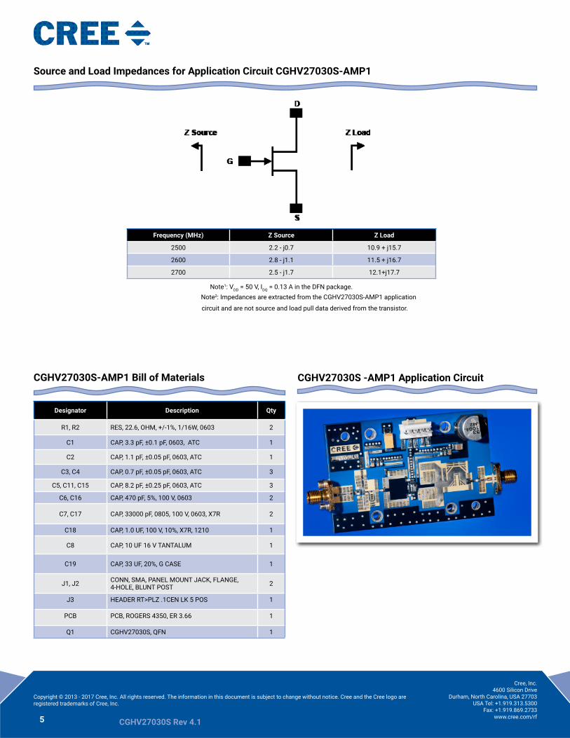
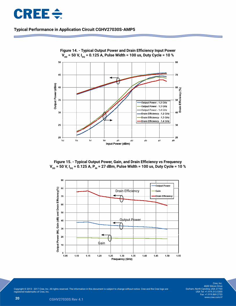
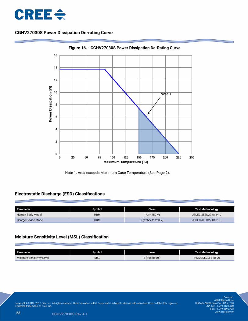
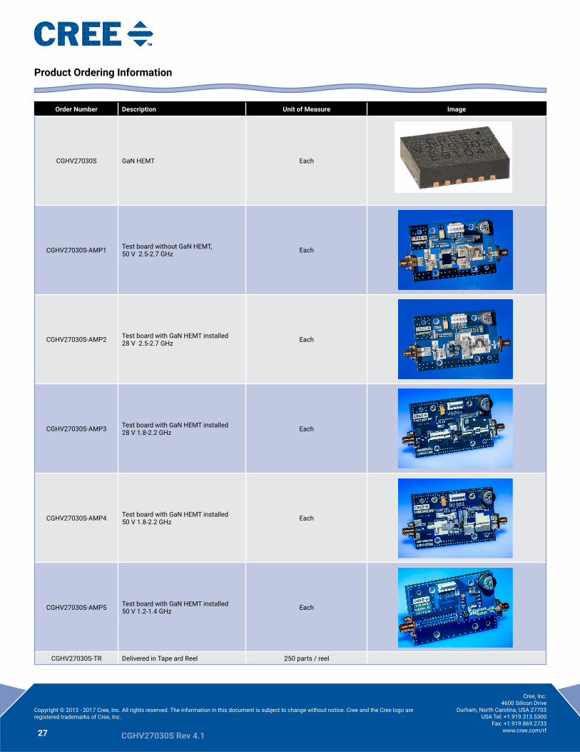