CAVITY PREPARATION/ASSEMBLY TECHNIQUES AND IMPACT...
27
CAVITY PREPARATION/ASSEMBLY TECHNIQUES AND IMPACT ON Q, REALISTIC Q – FACTORS IN A MODULE, REVIEW OF MODULES Peter Kneisel Jefferson Lab 12000 Jefferson Avenue, Newport News, VA 23606, USA Corresponding author: Peter Kneisel Jefferson Laboratory 12000 Jefferson Avenue Newport News, VA 23606, USA Phone: 757-269-7646 FAX: 757-269-7658 e-mail: [email protected] ABSTRACT This contribution summarizes the surface preparation procedures for niobium cavities presently used both in laboratory experiments and for modules, such as buffered chemical polishing (BCP), electropolishing (EP), high pressure ultrapure water rinsing (HPR), CO 2 snow cleaning and high temperature heat treatments for hydrogen degassing or post- purification. The impact of surface treatments and the degree of cleanliness during assembly procedures on cavity performance (Q – value and accelerating gradient E acc ) will be discussed. In addition, an attempt will be made to summarize the experiences made in module assemblies in different labs/projects such as DESY (TTF), Jlab (Upgrade) and SNS.
-
Upload
nguyencong -
Category
Documents
-
view
220 -
download
6
Transcript of CAVITY PREPARATION/ASSEMBLY TECHNIQUES AND IMPACT...
CAVITY PREPARATION/ASSEMBLY TECHNIQUES AND IMPACT ON
Q, REALISTIC Q – FACTORS IN A MODULE, REVIEW OF MODULES
Peter Kneisel
Jefferson Lab
12000 Jefferson Avenue, Newport News, VA 23606, USA
Corresponding author: Peter Kneisel
Jefferson Laboratory
12000 Jefferson Avenue
Newport News, VA 23606, USA
Phone: 757-269-7646
FAX: 757-269-7658
e-mail: [email protected]
ABSTRACT
This contribution summarizes the surface preparation procedures for niobium cavities
presently used both in laboratory experiments and for modules, such as buffered chemical
polishing (BCP), electropolishing (EP), high pressure ultrapure water rinsing (HPR), CO2
snow cleaning and high temperature heat treatments for hydrogen degassing or post-
purification. The impact of surface treatments and the degree of cleanliness during assembly
procedures on cavity performance (Q – value and accelerating gradient Eacc) will be
discussed.
In addition, an attempt will be made to summarize the experiences made in module
assemblies in different labs/projects such as DESY (TTF), Jlab (Upgrade) and SNS.

PACS: 29.27.Bd, 41.60.Cr
Keywords: Radio frequency, Superconductivity, Surface Treatment, Niobium, Cryo Modules
1
1. INTRODUCTION
Superconducting rf technology has become the “darling” of presently executed (SNS) and newly
proposed accelerator projects. These include applications such as energy recovery linacs (ERL),
free electron lasers (FEL), proton drivers, accelerators for transmutation of nuclear waste and
most recently the recommendation by the International Technology Recommendation Panel
(ITRP) for the International Linear Collider (ILC). The reasons for this popularity are
astonishing advances in the technology over the last few years, promising better performances of
the proposed devices and reduced capital and operational costs. In some instances like e.g. cw
machines with high accelerating gradients such as ERL’s this technology seems to be the only
choice for verifying such designs.
The technology has come a long way since its early application four decades ago at Stanford
University [1]. Many technological obstacles such as multipacting, early quenches due to
defects in the material, high residual resistances (low Q-values) or excessive non-resonant
electron loading (“field emission”) due to contaminated surfaces had to be overcome to
arrive at “present-day” performance levels in niobium cavities – the material of choice for
accelerator application – which in some instances have been close or even have reached the
fundamental limits of the superconducting material. Key to these advances has been a better
understanding of material properties, both surface and bulk properties, and physical
phenomena caused by the interplay between electro-magnetic fields in the cavities and the
state of the cavity surfaces. Also, improved procedures to protect the sensitive cavity surfaces
from contamination – after all in rf superconductivity only a few nanometer of the material
are determining the performance of a cavity – have contributed significantly to the nowadays
achievable performance levels of cavities.
2
In the following chapters (2-4), established and developing techniques for preparation of high
performance rf cavity surfaces are being reviewed along with assembly techniques to
preserve the necessary cleanliness levels and to avoid re-contamination.
In chapter 5 the performances of cryo-modules in large scale projects such as SNS, TTF/DESY
and Jlab’s Upgrade are reviewed.
2. “STANDARD” CAVITY SURFACE TREATMENTS
The performance of an accelerator cavity is determined by the dependence of its Q–value on
accelerating gradient. The goal is to achieve a performance as close as possible to the theoretical
limit of the superconducting material. The Q–value, which is inversely proportional to the
surface resistance, is given by the BCS theory and the achievable accelerating gradient is
determined by the associated peak magnetic field on the cavity surface, at which the
superconductor is transitioning into the normal conducting state – the critical magnetic field,
approximately 185 mT for niobium at 2 K. As an example, Figure 1 shows the frequency
dependence of the BCS surface resistance for niobium at a temperature of 2K, which is in many
cases the operating temperature for cavities of a frequency above ~ 700 MHz. However, the BCS
theory describes the ideal surface resistance at low surface fields; realistically, there is not only
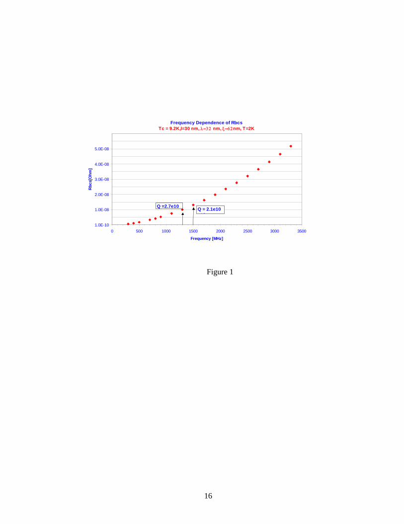
an additive contribution to the BCS behavior – the residual resistance Rres – but also a field
dependence as schematically shown in figure 2. At the high end of the Q vs E – curve a strong
degradation of the Q-value is often observed. The physics of this “Q–drop” is still not completely
understood, however it has become clear that oxygen diffusion from the surface into the material
plays a role, since “in situ” baking of a cavity at 120C for long periods of time ( > 24 hrs)
improves the high field Q–values [2].
The purpose of the treatment of a niobium cavity surface is to achieve an “ideal” surface as
closely as possible.
3
Niobium cavity surfaces are damaged by the fabrication process, starting from the rolled and
annealed sheet material through the forming, machining and electron beam welding processes. In
order to achieve good performances of cavities this “damage layer” has to be removed. Figure 3
shows the results from a series of experiments, during which material has been successively
removed from a cavity surface and the residual surface resistance at low fields and the maximal
achievable surface electric fields have been determined. It is obvious that at least a layer of 100
micron has to be removed to achieve low residual resistances (high Q–values) and even more for
high gradients [3].
To achieve this “ideal” surface – free of defects, damages, contamination and residue from
handling procedures – a series surface treatment procedures have been developed over the years
at various labs involved in SRF technology, which have led to the mature technology available
nowadays. The commonly used procedures are listed and discussed below:
• Eddy current scanning and squid scanning of niobium sheets prior to cavity fabrication
to detect defects in the material: This QA procedure has been successfully developed at
DESY for the 9-cell cavities for the TESLA Test Facility (TTF) [4, 5]. The resolution for
the eddy current system is limited to defects of app. 100 micron, whereas the squid
system [6] provides a resolution of < 50 micron.
• Degreasing of the cavities under ultrasonic agitation: this method is routinely used with
detergents or solvents to remove greasy or oily residue from fabrication processes and
finger prints.
• Buffered chemical polishing to remove the surface damage layer: the solution consists of
an acid mixture of hydrofluoric (40%), nitric (69%) and phosphoric (86%) acids of
mixing ratios 1:1:1, 1:1:2 or 1:1:4. The more buffered solutions provide lower removal
rates and therefore a better control of the exothermic reaction. The chemical treatment is
done at room temperature for smaller cavities; more typical for larger cavities a 1:1:2
4
mixture at a temperature around 10C is used to avoid excessive pick-up of evolving
hydrogen gas from the process [7].
• Electropolishing (EP) is used to remove the surface damage layer and to achieve a very
smooth surface finish on the niobium. The electropolishing process for niobium was
developed in 1971 [8] with a solution of hydrofluoric and conc. sulfuric acids in a 1:9
ratio. The process has a leveling effect on the surfaces since higher electric fields are
established in the bath at surface protrusions and therefore the removal rate at these sites
is higher. The original process controlled the current oscillations occurring during the
electropolishing; later the process was improved at KEK to a continuous process [9] for
horizontally rotating cavity arrangements. EP is presently used/developed at several
laboratories such as KEK, DESY, Saclay, Cornell and Jlab. It has been demonstrated on
many occasions [10] that superior cavity performances can be achieved with
electropolished surfaces.
• “Barrel” polishing with plastic stones, an abrasive powder and water: this process has
been developed at KEK to mechanically remove imperfections on the cavity surface
resulting from the fabrication process such as surface cracks, rough electron beam welds
or weld splatter. The process is rather slow, but by adding an additional motion
(“Centrifugal barrel polishing”) during the process as schematically indicated in figure 4
the removal rate was increased to app. 4 micron/hr [11]. By replacing the water with a
hydrogen-free agent such as e.g. FC-77 the niobium was kept hydrogen-free and the need
for hydrogen degassing was eliminated, stream-lining the whole surface treatment
process [12].
• High Pressure Ultrapure Water Rinsing is universally used as a final step in the surface
preparation of a niobium accelerating cavity. Ultrapure water jets of a resistivity > 18
MΩcm are directed at the cavity surfaces at a pressure of ~ 100 bar (1200 psi) through
5
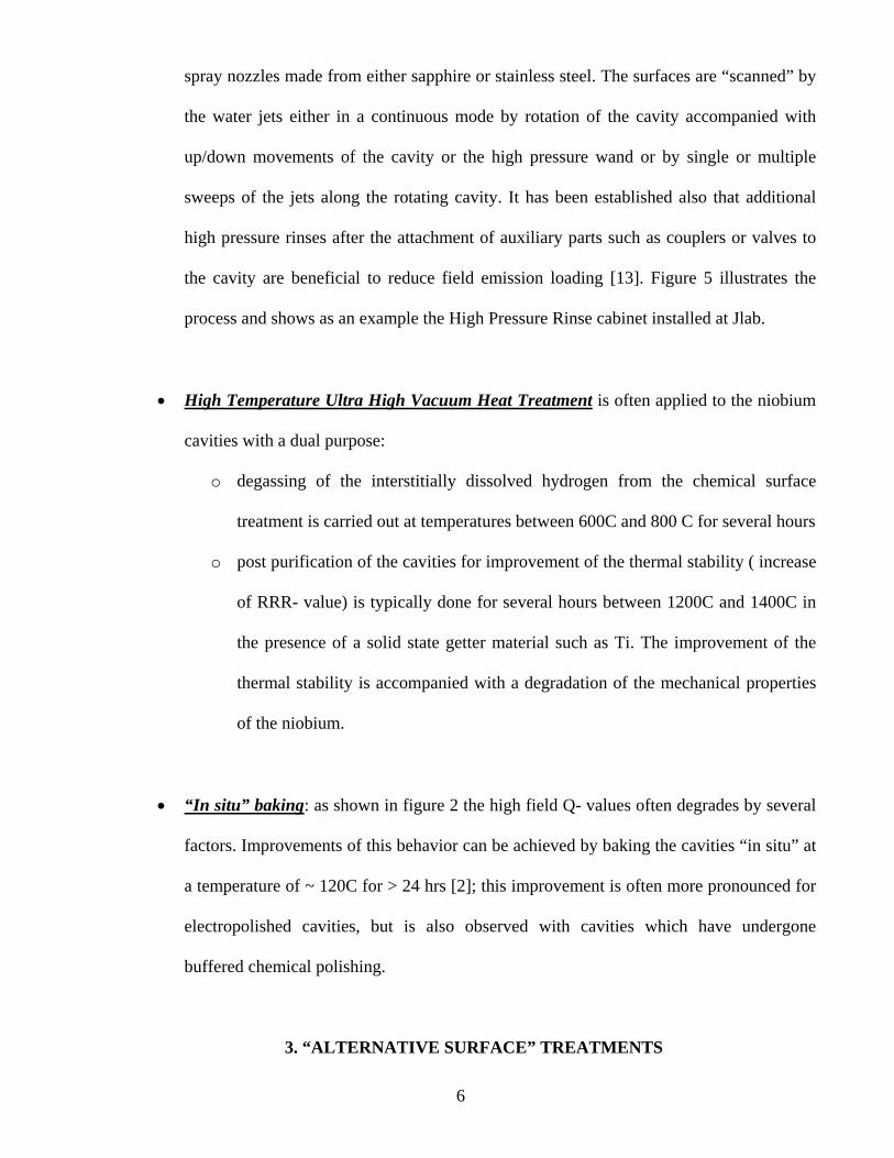
spray nozzles made from either sapphire or stainless steel. The surfaces are “scanned” by
the water jets either in a continuous mode by rotation of the cavity accompanied with
up/down movements of the cavity or the high pressure wand or by single or multiple
sweeps of the jets along the rotating cavity. It has been established also that additional
high pressure rinses after the attachment of auxiliary parts such as couplers or valves to
the cavity are beneficial to reduce field emission loading [13]. Figure 5 illustrates the
process and shows as an example the High Pressure Rinse cabinet installed at Jlab.
• High Temperature Ultra High Vacuum Heat Treatment is often applied to the niobium
cavities with a dual purpose:
o degassing of the interstitially dissolved hydrogen from the chemical surface
treatment is carried out at temperatures between 600C and 800 C for several hours
o post purification of the cavities for improvement of the thermal stability ( increase
of RRR- value) is typically done for several hours between 1200C and 1400C in
the presence of a solid state getter material such as Ti. The improvement of the
thermal stability is accompanied with a degradation of the mechanical properties
of the niobium.
• “In situ” baking: as shown in figure 2 the high field Q- values often degrades by several
factors. Improvements of this behavior can be achieved by baking the cavities “in situ” at
a temperature of ~ 120C for > 24 hrs [2]; this improvement is often more pronounced for
electropolished cavities, but is also observed with cavities which have undergone
buffered chemical polishing.
3. “ALTERNATIVE SURFACE” TREATMENTS
6
Here we will discuss
• Alternative cleaning methods such as CO2 Snow
Among the various alternative surface cleaning techniques [14] CO2-Snow cleaning is being
developed at DESY as an alternative to high pressure water rinsing or as an “in situ” cleaning
technique for assembled modules [13]. The method has been applied successfully to samples,
which were after cleaning investigated at the University of Wuppertal with respect to their dc
field emission behaviour [15]. Even though an optimization of the process is necessary
(avoidance of condensation, mass flow optimization), preliminary tests on single cell cavities
showed encouraging results and gradients up to Eacc = 33 MV/m were measured.
A production system is presently under construction and will be completed in autumn of
2005.
• Large grain/single crystal cavities
It has recently been recognized that ingot niobium material with very large grains or single
crystals has very good mechanical properties such as elongation and can easily be formed
into cavities. In addition, buffered chemical polishing provides on this material very smooth
surfaces, which are believed to be necessary for high performance cavities as experienced
with electropolished surfaces. Figure 6 compares the surface roughness of a buffered
chemically polished niobium single crystal to a surface of fine grain material [16]. A nearly
50 times smoother surface results from the bcp of a single crystal and compared to an
electropolished fine grain surface a gain of about a factor of 10 in smoothness has been
measured ( RMS roughness of 27 nm for single crystal vs 251 nm of electropolished fine
grain niobium).
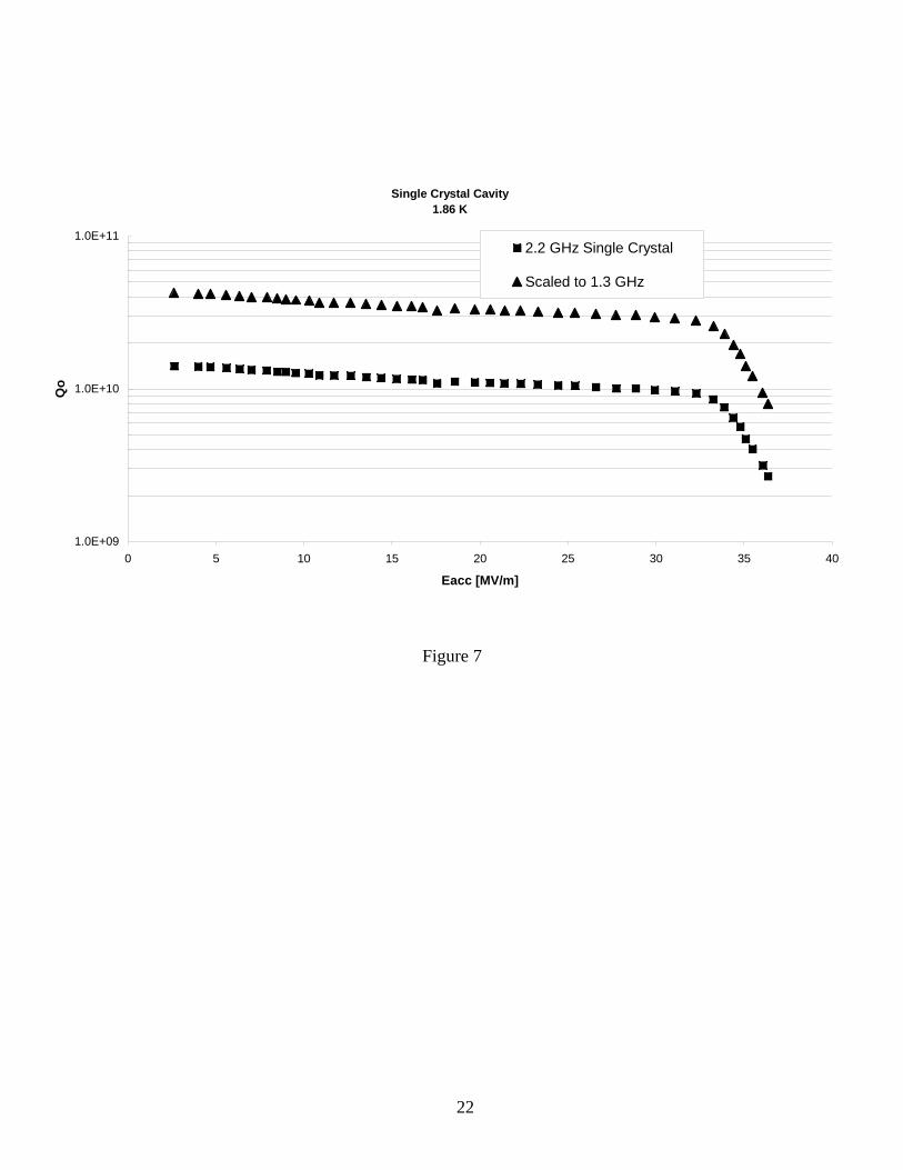
The rf performance of a single cell single crystal cavity at 2.2 GHz is shown in figure 7
together with scaled values for a frequency of 1300 MHz, a most likely frequency for an
7
ERL device. This “new” technology seems to provide not only excellent cavity
performances, but also promises potential advantages such as reduced cost for the material
and the cavities, less elaborate QA and surface treatment procedures and better mechanical
properties of the material.
4. COMPARISON OF TTF MODULE AND SNS MODULE ASSEMBLY PROCEDURES
It is widely accepted that the obstacles to good cavity performance are insufficient material
removal, defects in the material and contamination of the sensitive surfaces (field emission). All
applied procedures need to deal with these problems and the most difficult is the control of
contamination. The level of contamination is different in the different laboratories and depends
on the infra-structure, the design of the cavities/modules, the auxiliary parts to the cavities such
as bolts, gaskets, or couplers and most importantly on the people. The optimum procedures have
to be developed for each lab and each project. The following comparison as listed in table 1 and
2 between procedures applied at DESY to the TTF modules ( # 1 – 5) [17] and 23 modules for
the SNS project at Jlab points out the common procedures, but also the different approaches on
various details.
The assembly of a TTF string in the clean room at DESY is shown in figure 8.
5. CRYOMODULE PERFORMANCES
Whereas many data are available for individual cavity performances, cryo-modules on a
larger scale have only been tested in recent years for the TTF-, SNS- and Jlab Upgrade
projects.
a) TTF
8
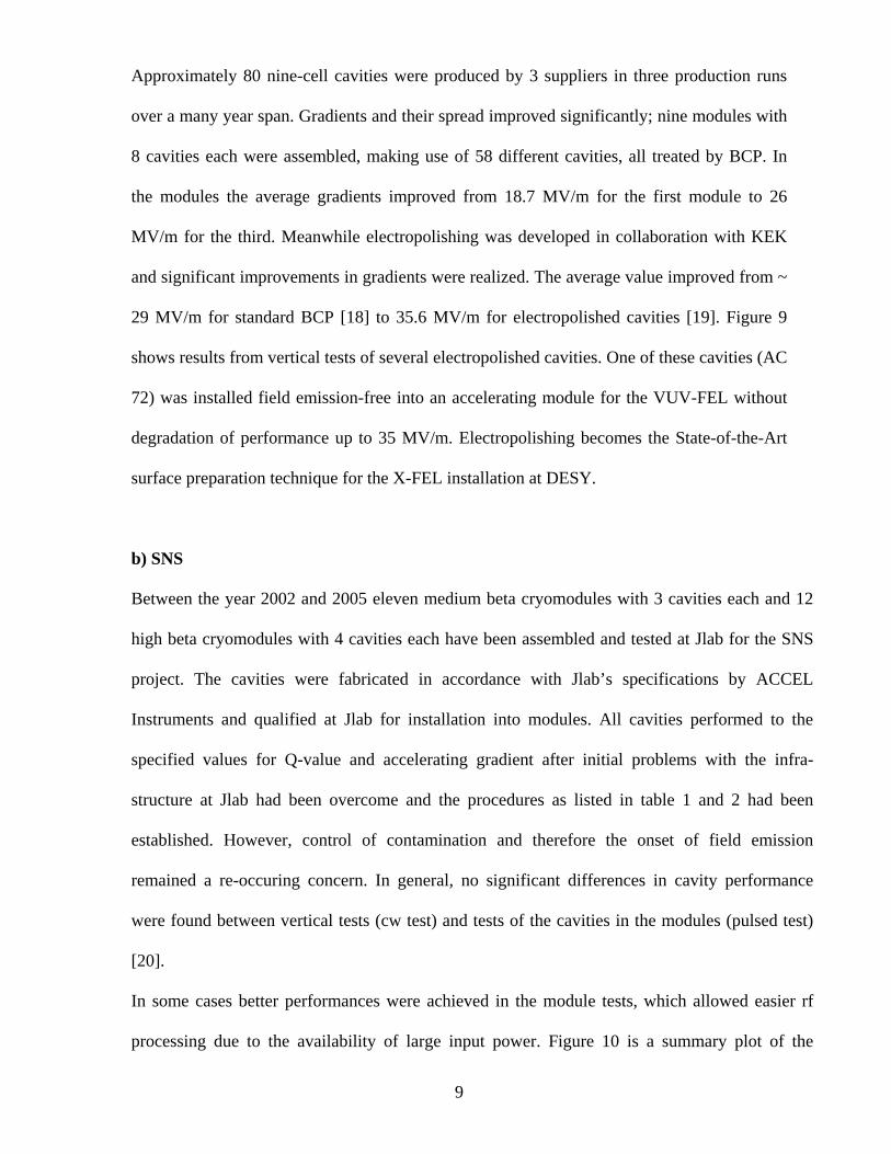
Approximately 80 nine-cell cavities were produced by 3 suppliers in three production runs
over a many year span. Gradients and their spread improved significantly; nine modules with
8 cavities each were assembled, making use of 58 different cavities, all treated by BCP. In
the modules the average gradients improved from 18.7 MV/m for the first module to 26
MV/m for the third. Meanwhile electropolishing was developed in collaboration with KEK
and significant improvements in gradients were realized. The average value improved from ~
29 MV/m for standard BCP [18] to 35.6 MV/m for electropolished cavities [19]. Figure 9
shows results from vertical tests of several electropolished cavities. One of these cavities (AC
72) was installed field emission-free into an accelerating module for the VUV-FEL without
degradation of performance up to 35 MV/m. Electropolishing becomes the State-of-the-Art
surface preparation technique for the X-FEL installation at DESY.
b) SNS
Between the year 2002 and 2005 eleven medium beta cryomodules with 3 cavities each and 12
high beta cryomodules with 4 cavities each have been assembled and tested at Jlab for the SNS
project. The cavities were fabricated in accordance with Jlab’s specifications by ACCEL
Instruments and qualified at Jlab for installation into modules. All cavities performed to the
specified values for Q-value and accelerating gradient after initial problems with the infra-
structure at Jlab had been overcome and the procedures as listed in table 1 and 2 had been
established. However, control of contamination and therefore the onset of field emission
remained a re-occuring concern. In general, no significant differences in cavity performance
were found between vertical tests (cw test) and tests of the cavities in the modules (pulsed test)
[20].
In some cases better performances were achieved in the module tests, which allowed easier rf
processing due to the availability of large input power. Figure 10 is a summary plot of the
9
gradients at the specified Q-value of 5 x 10⁹ measured over a two year span between October
2002 and October 2004; it shows both some “seasonal” variation in performance and a rather
wide spread, indicative of some QA and infra-structure problems with the facilities at Jlab.
c) Jlab Upgrade
At Jlab three different modules have been developed since the initial installation of CEBAF.
Two of these modules were used for the FEL with the modification of the original cavity design
from five cell cavities to 7-cell cavities and a replacement of the waveguide HOM couplers with
coaxial-DESY type HOM couplers [21]. The cavities are stably operated at Eacc = 15 MV/m in
the FEL [22].
A new module, named “Renascence”, has been developed with two different 7-cell cavity
geometries: a high gradient (HG) cavity optimized for accelerating gradient and a low loss (LL)
cavity minimizing the cryogenic losses [23]. The design goals for these cavities in a module are a
gradient of ~ 20 MV/m with a Q-value at 2.05K of Q = 8x10⁹. Several cavities of each geometry
have been fabricated “in house” at Jlab and have been qualified in vertical tests [24]. Results are
shown in figure 11. The cavities have been assembled into a cavity string and the assembly into
the cryostat is nearly complete. Test of the module is expected to take place in summer 2005.
6. CONCLUSION
The preparation and assembly of niobium multi-cell cavities into cavity strings/cryomodules has
matured to a point, where one can achieve accelerating gradients Eacc > 15 MV/m with Q –
values of Q > 8 x 10⁹ at 2K. However, field emission is still the major obstacle to achieve these
performance levels on a regular basis and stringent contamination control measures have to be
applied. At gradients above 20-24 MV/m a not yet fully understood “Q – drop” is encountered,
which can be overcome – in most cases – by “in-situ” baking at ~ 120 C for many hours. This
10
improvement seems to be more consistent on electropolished cavities, but it is also observed with
buffered chemically polished surfaces.
Finally, as already pointed out above, the optimum procedures are facility and project specific
and cavity performances seem to be “local”, depending a lot on well trained personnel.
.
ACKNOWLEDGEMENTS
Many colleagues have provided me with information for this contribution and I used figures
from presentations by several colleagues, whom I want to thank for their support: C. Reece, Jlab,
J. Ozelis, Jlab, H. Whitehead, Jlab, A. Matheisen, DESY, L. Lilje, DESY, H. Weise, DESY, W.
Singer, DESY and D. Reschke, DESY.
FIGURE CAPTIONS
Figure 1. Frequency Dependence of the BCS Surface Resistance for niobium
Figure 2. Schematic of the often observed dependence of Q-value on accelerating gradient in
high purity niobium cavities
Figure 3. Improvement of niobium cavity performance by successive removal of the surface
damage layer
Figure 4. Centrifugal barrel polishing as developed at KEK
Figure 5. High Pressure Ultrapure Water rinsing facility at Jlab
Figure 6. Comparison of surface roughness achieved with BCP on single crystal and fine grain
niobium
Figure 7. Performance of a single crystal niobium cavity at 2.2 GHz. The Q – values are in
addition scaled to a frequency of 1.3 GHz
11
Figure 8. Assembly of a TTF cavity string in the class 10 clean room at DESY
Figure 9. Experimental results achieved on 9-cell TTF cavities during vertical testing after
electropolishing surface treatment
Figure 10. Summary of results from SNS cavity tests during October 2002 and October 2004
Figure 11. Vertical test performance of 7-cell cavities for the “Renascence” cryomodule at Jlab
REFERENCES
[1] H. A. Schwettman et al.; International. Advances in Cryogenic Engineering (New York, Plenum Press, 1965), p.88 [2] B. Visentin, Proc. of the 11th Workshop on RF Superconductivity, Travemuende, Germany (2003) paper TuO01, https://srf2003.desy.de/sl-srf/ [3] P. Kneisel and B. Lewis, Proc. of the 7th Workshop on RF Superconductivity, Gif-sur-Yvette, France (1995), p. 311 [4] W. Singer, D. Proch, A. Brinkmann; Proc. of the 8th Workshop on RF Superconductivity, Abano Terme, Italy (1997), p. 850 [5] W. Singer; http://www-bd.fnal.gov/niobium/program.html[6] http://www-mhf.desy.de/public/care04/2004.11.03_sr3/wp6_wuppertal_singer_palmieri.pdf [7] B. Bonin, R.W. Roeth; Proc. of the 5th Workshop on RF Superconductivity, Hamburg, Germany 91991), p. 210 [8] H. Diepers et al.; Physics Letters 37A(2), 139 (1971) [9] K. Saito et al.; Proc. Of the 4th Workshop on RF Superconductivity, KEK, Tsukuba, Japan (1989), p. [10] e.g. K. Saito; http://accelconf.web.cern.ch/accelconf/p03/PAPERS/ROAA002.PDF [11] T. Higuchi et al.; http://conference.kek.jp/SRF2001, paper PR022 [12] T. Higuchi, K. Saito, https://srf2003.desy.de, paper We015 [13] D. Reschke; ANL Report 05/10, Argonne National Lab (2005), p.30 [14] P. Kneisel, B. Lewis; Proc. of the 7th Workshop on RF Superconductivity, Gif-sur-Yvette, France (1995), p.311 [15] L. Lilje et al.; http://wwwmhf.desy.de/public/care04/2004.11.03_sr3/wp5_summary_ll_200410.pdf [16] A. Wu, Jlab, private communications [17] A. Matheisen; http://lcdev.kek.jp/ILCWS/Talks/13wg5-02-FabProc_Matheisen.pdf [18] H. Weise; http://adweb.desy.de/~weise/: [19] L. Lilje; http://bel.gsi.de/linac2004/PAPERS/WE102.PDF [20] J. Ozelis, Jlab, private communications [21] J. Delayen, Proc. of the 9th Workshop on RF Superconductivity, Santa Fe, New Mexico (1999), Paper TuP019 [22] A.M. Valente et al.; http://accelconf.web.cern.ch/accelconf/e04, paper TUPKF 072 [23] J. Sekutowicz et al.; http://accelconf.web.cern.ch/accelconf/p03, paper TPAB 085 [24] C. Reece; ANL Report 05/10, Argonne National Lab (2005) p.210
12

13
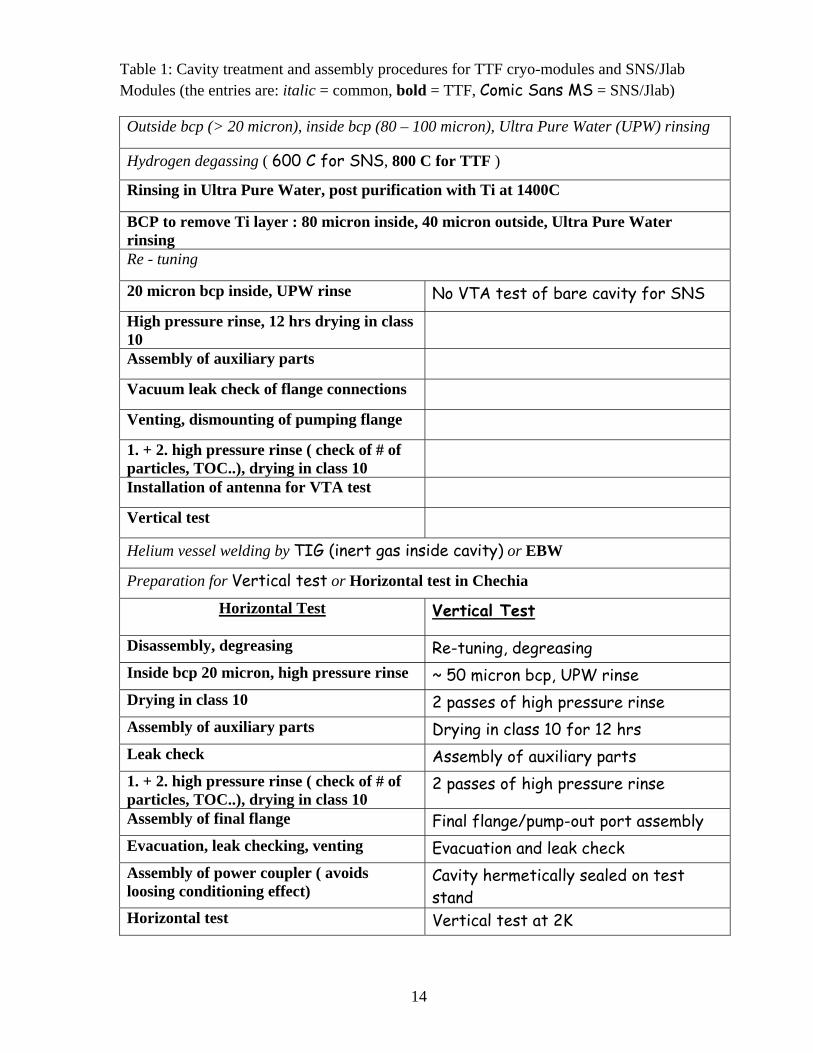
Table 1: Cavity treatment and assembly procedures for TTF cryo-modules and SNS/Jlab Modules (the entries are: italic = common, bold = TTF, Comic Sans MS = SNS/Jlab)
Outside bcp (> 20 micron), inside bcp (80 – 100 micron), Ultra Pure Water (UPW) rinsing
Hydrogen degassing ( 600 C for SNS, 800 C for TTF )
Rinsing in Ultra Pure Water, post purification with Ti at 1400C
BCP to remove Ti layer : 80 micron inside, 40 micron outside, Ultra Pure Water rinsing Re - tuning
20 micron bcp inside, UPW rinse No VTA test of bare cavity for SNS High pressure rinse, 12 hrs drying in class 10
Assembly of auxiliary parts
Vacuum leak check of flange connections
Venting, dismounting of pumping flange
1. + 2. high pressure rinse ( check of # of particles, TOC..), drying in class 10
Installation of antenna for VTA test
Vertical test
Helium vessel welding by TIG (inert gas inside cavity) or EBW
Preparation for Vertical test or Horizontal test in Chechia
Horizontal Test Vertical Test
Disassembly, degreasing Re-tuning, degreasing Inside bcp 20 micron, high pressure rinse ~ 50 micron bcp, UPW rinse Drying in class 10 2 passes of high pressure rinse Assembly of auxiliary parts Drying in class 10 for 12 hrs Leak check Assembly of auxiliary parts 1. + 2. high pressure rinse ( check of # of particles, TOC..), drying in class 10
2 passes of high pressure rinse
Assembly of final flange Final flange/pump-out port assembly Evacuation, leak checking, venting Evacuation and leak check Assembly of power coupler ( avoids loosing conditioning effect)
Cavity hermetically sealed on test stand
Horizontal test Vertical test at 2K
14
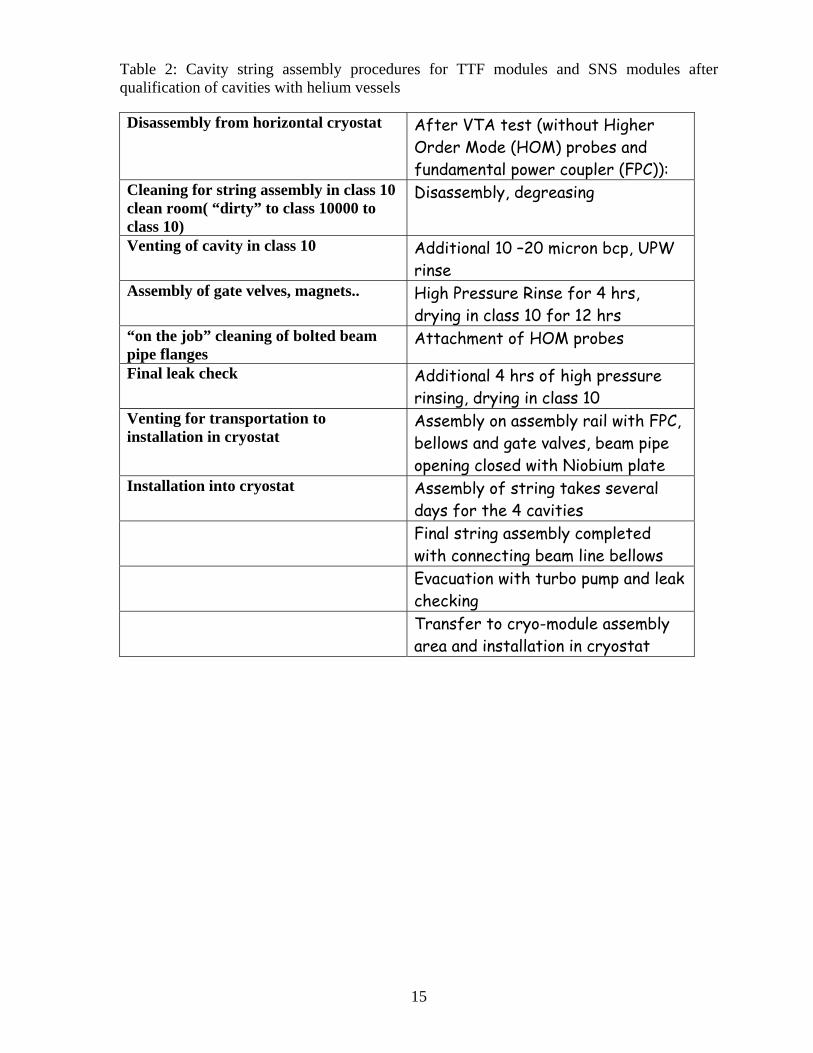
Table 2: Cavity string assembly procedures for TTF modules and SNS modules after qualification of cavities with helium vessels
Disassembly from horizontal cryostat After VTA test (without Higher Order Mode (HOM) probes and fundamental power coupler (FPC)):
Cleaning for string assembly in class 10 clean room( “dirty” to class 10000 to class 10)
Disassembly, degreasing
Venting of cavity in class 10 Additional 10 –20 micron bcp, UPW rinse
Assembly of gate velves, magnets.. High Pressure Rinse for 4 hrs, drying in class 10 for 12 hrs
“on the job” cleaning of bolted beam pipe flanges
Attachment of HOM probes
Final leak check Additional 4 hrs of high pressure rinsing, drying in class 10
Venting for transportation to installation in cryostat
Assembly on assembly rail with FPC, bellows and gate valves, beam pipe opening closed with Niobium plate
Installation into cryostat Assembly of string takes several days for the 4 cavities
Final string assembly completed with connecting beam line bellows
Evacuation with turbo pump and leak checking
Transfer to cryo-module assembly area and installation in cryostat
15
Frequency Dependence of RbcsTc = 9.2K,l=30 nm, λ=32 nm, ξ=62nm, T=2K
1.0E-10
1.0E-08
2.0E-08
3.0E-08
4.0E-08
5.0E-08
0 500 1000 1500 2000 2500 3000 3500
Frequency [MHz]
Rbc
s[O
hm]
Figure 1
Q =2.7e10 Q = 2.1e10 10
16
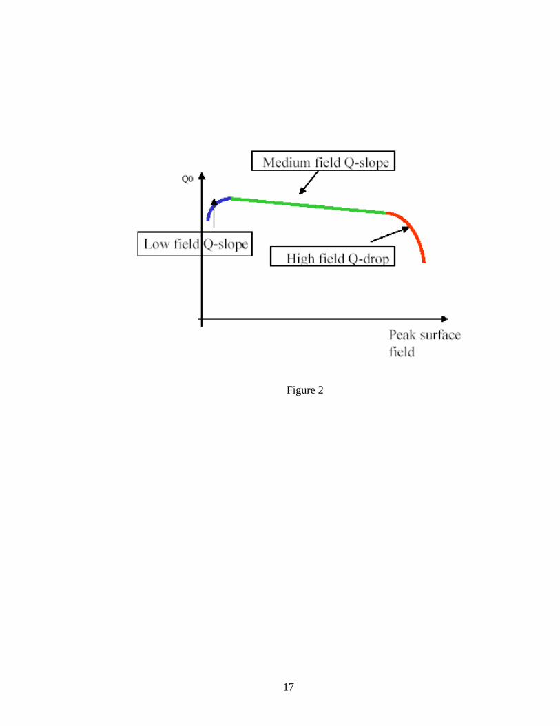
Figure 2
17
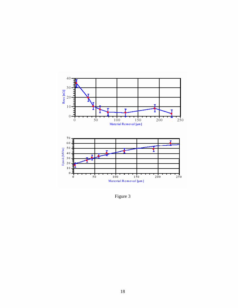
Figure 3
18
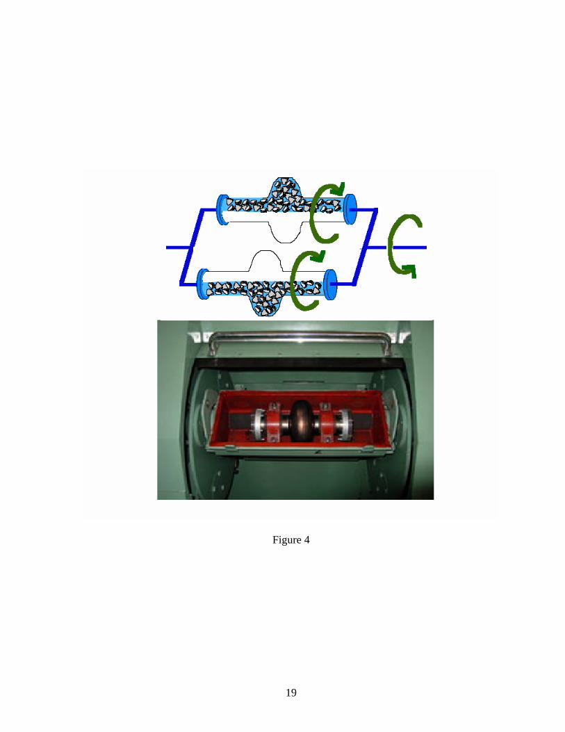
Figure 4
19
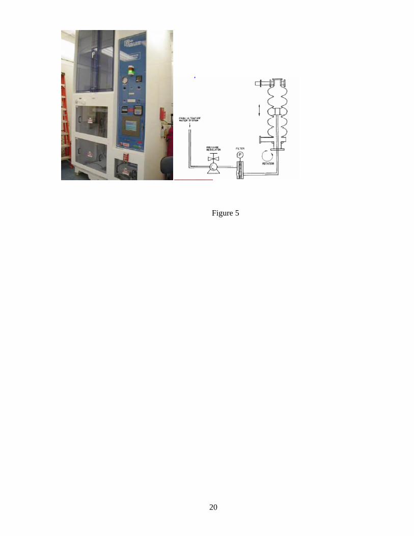
Figure 5
20
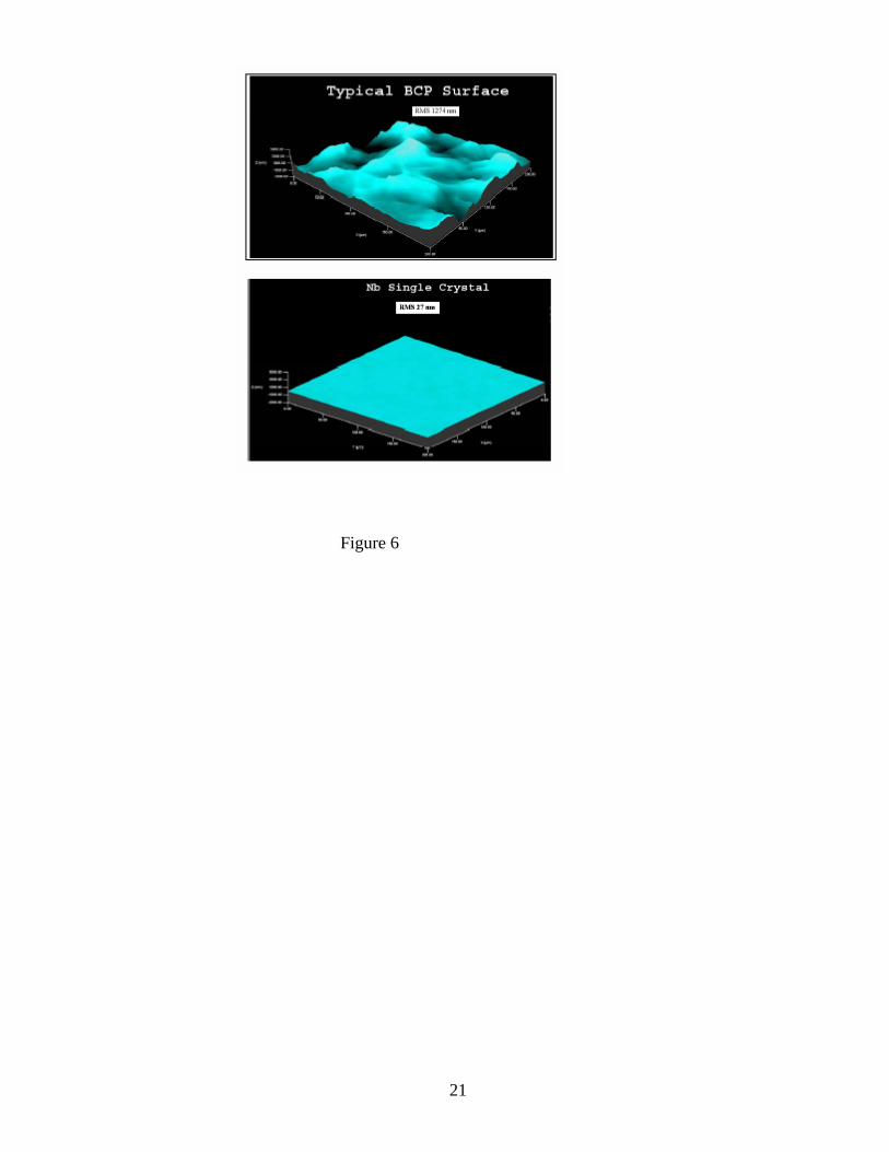
Figure 6
21
Single Crystal Cavity1.86 K
1.0E+09
1.0E+10
1.0E+11
0 5 10 15 20 25 30 35 40
Eacc [MV/m]
Qo
2.2 GHz Single Crystal
Scaled to 1.3 GHz
Figure 7
22
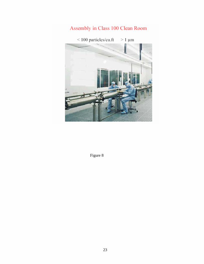
Figure 8
23
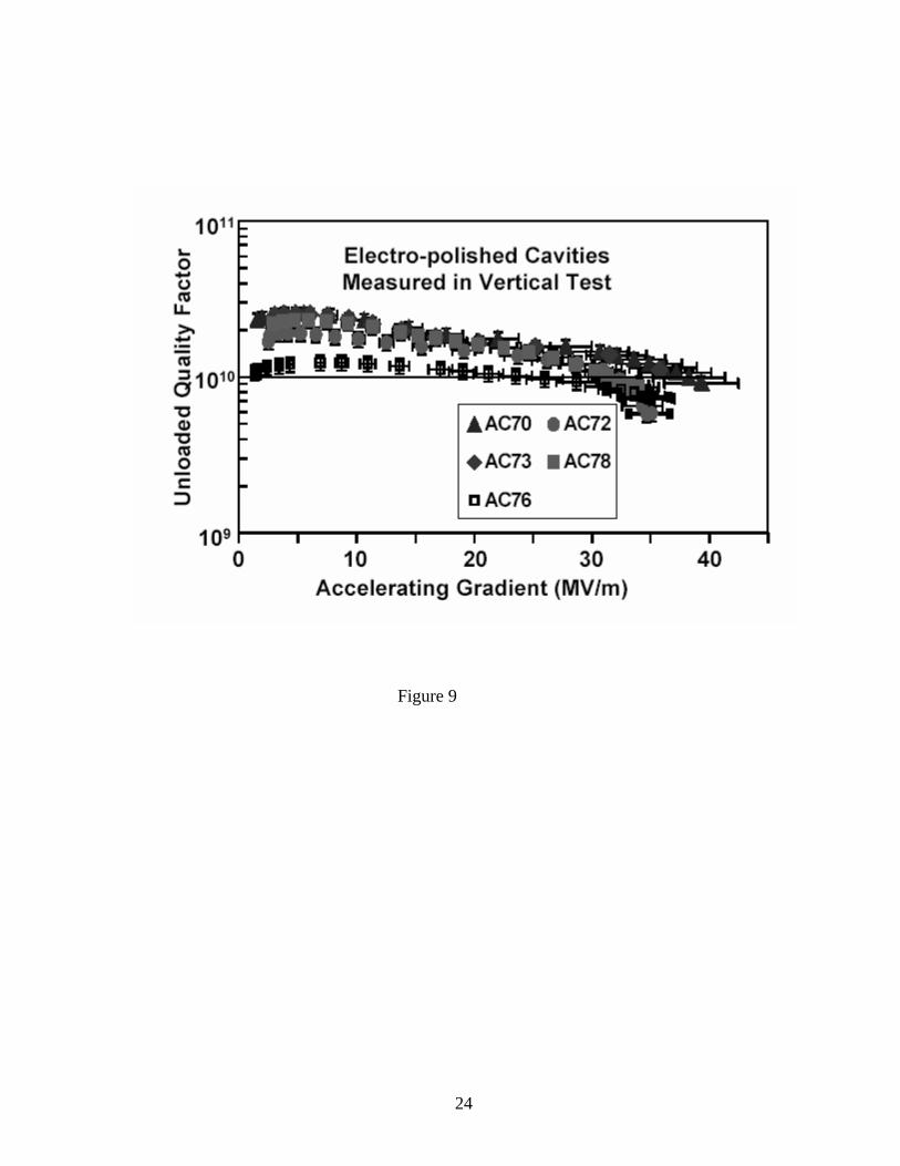
Figure 9
24
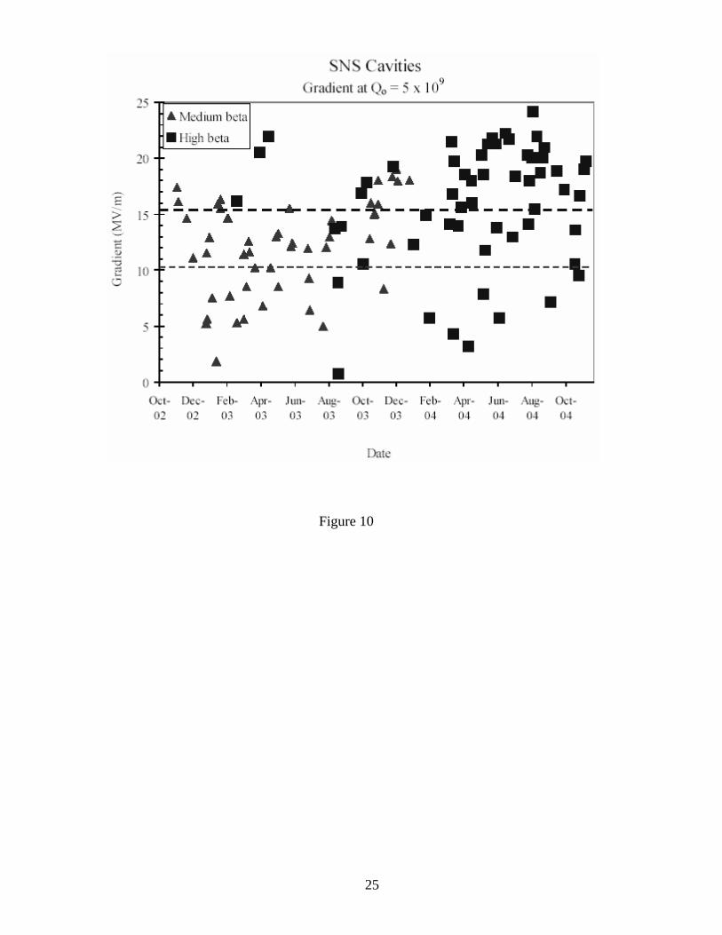
Figure 10
25
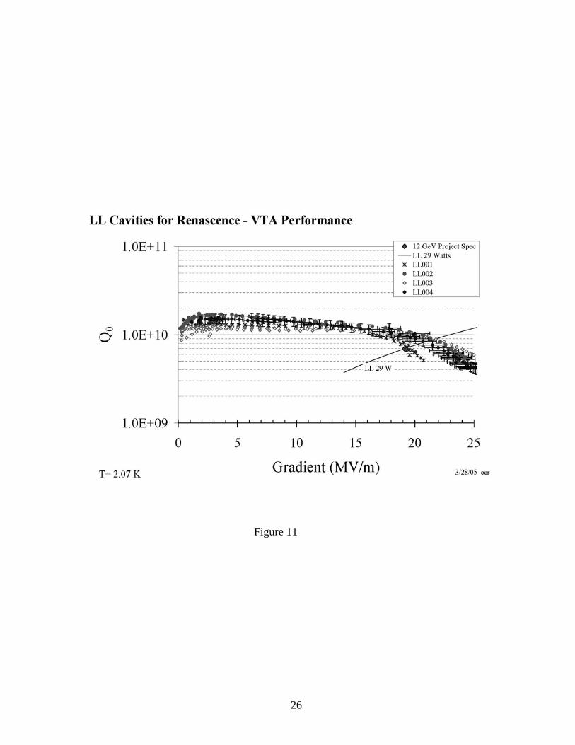
Figure 11
26