Cascaded Two-Level Inverter-Based Multi-Level …ijsrset.com/paper/2254.pdfPower Applications by...
10
IJSRSET173194 | Received : 05 Feb -2017 | Accepted : 20 Feb-2017 | January-February-2017 [(3)1: 397-406] © 2017 IJSRSET | Volume 3 | Issue 1 | Print ISSN: 2395-1990 | Online ISSN : 2394-4099 Themed Section: Engineering and Technology 397 Cascaded Two-Level Inverter-Based Multi-Level Inverter for High Power Applications by Using Statcom with Fuzzy Logic Control V. Madhavi 1 , K. Nagabhushanam 2 1,2 Department of EEE, JNTU Anantapur, Andhra Pradesh, India ABSTRACT This paper presents a simple STATCOM scheme using a cascaded two-level inverter-based multilevel inverter. The proposed topologies have two VSI based two-level inverters are connected in cascade through open-end windings of a three-phase transformer and filter elements. Converter fed dc-link voltages are regulates at different levels to obtain four-level operation. The proposed STATCOM multilevel inverter has operates under MATLAB/SIMULINK environment and the results are verified in balanced and unbalanced conditions. Further, stability behavior of the topology is investigated. The system behaviors are analyzing under various operating conditions using fuzzy logic control. Keywords : DC-link voltage balance, multilevel inverter, power quality (PQ), static compensator (STATCOM). I. INTRODUCTION The application of flexible ac transmission systems(FACTS) controllers, such as static compensator(STATCOM) and static synchronous series compensator(SSSC) is increasing in power systems. This is due to theirability to stabilize the transmission systems and to improve power quality (PQ) in distribution systems. STATCOM is popularly accepted as a reliable reactive power controller replacing conventional var compensators, such as the thyristor- switchedcapacitor (TSC) and thyristor-controlled reactor (TCR). This device provides reactive power compensation, active power oscillation damping, flicker attenuation, voltage regulation, etc.[1]. Generally, in high-power applications, var compensation is achieved using multilevel inverters [2]. These inverters consist of a large number of dc sources which are usually realized by capacitors. Hence, the converters draw a small amount of activepower to maintain dc voltage of capacitors and to compensate the losses in the converter. However, due to mismatch in conduction and switching losses of the switching devices, the capacitors voltages are unbalanced. Balancing these voltages is a major research challenge in multilevel inverters. Various control schemes using different topologies are reported in [3]–[7]. Among the three conventional multilevel inverter topologies.cascade H-bridge is the most popular for static var compensation [5], [6]. However, the aforementioned topology requires a large number of dc capacitors. The control of individual dc-link voltage of the capacitors is difficult. Static var compensation by cascading conventional multilevel/two level inverters is an attractive solution for high-power applications. The topology consists of standard multilevel/two level inverters connected in cascade through open-end windings of a three-phase transformer. Such topologies are popular in high-power drives [8]. One of the advantages of this topologyis that by maintaining asymmetric voltages at the dc links of the inverters, the number of levels in the output voltage waveform can be increased. This improves PQ [8]. Therefore, overall control is simple compared to conventional multilevel inverters.Various var compensation schemes based on this topology are reported in [10]–[12]. In [10], a three- level inverter and two level inverter are connected on either side of the transformer low-voltage winding. The dc-link voltages are maintained by separate converters. In [11], three-level operation is obtained by using standard two-level inverters. The dc-link voltage balance between the inverters is affected by the reactive power supplied to the grid. In this paper, a static var compensation scheme is proposed for a cascaded two-level inverter-based
Transcript of Cascaded Two-Level Inverter-Based Multi-Level …ijsrset.com/paper/2254.pdfPower Applications by...

IJSRSET173194 | Received : 05 Feb -2017 | Accepted : 20 Feb-2017 | January-February-2017 [(3)1: 397-406]
© 2017 IJSRSET | Volume 3 | Issue 1 | Print ISSN: 2395-1990 | Online ISSN : 2394-4099 Themed Section: Engineering and Technology
397
Cascaded Two-Level Inverter-Based Multi-Level Inverter for High Power Applications by Using Statcom with Fuzzy Logic Control
V. Madhavi1, K. Nagabhushanam2
1,2Department of EEE, JNTU Anantapur, Andhra Pradesh, India
ABSTRACT
This paper presents a simple STATCOM scheme using a cascaded two-level inverter-based multilevel inverter. The
proposed topologies have two VSI based two-level inverters are connected in cascade through open-end windings of
a three-phase transformer and filter elements. Converter fed dc-link voltages are regulates at different levels to
obtain four-level operation. The proposed STATCOM multilevel inverter has operates under MATLAB/SIMULINK
environment and the results are verified in balanced and unbalanced conditions. Further, stability behavior of the
topology is investigated. The system behaviors are analyzing under various operating conditions using fuzzy logic
control.
Keywords : DC-link voltage balance, multilevel inverter, power quality (PQ), static compensator (STATCOM).
I. INTRODUCTION
The application of flexible ac transmission
systems(FACTS) controllers, such as static
compensator(STATCOM) and static synchronous series
compensator(SSSC) is increasing in power systems.
This is due to theirability to stabilize the transmission
systems and to improve power quality (PQ) in
distribution systems. STATCOM is popularly accepted
as a reliable reactive power controller replacing
conventional var compensators, such as the thyristor-
switchedcapacitor (TSC) and thyristor-controlled
reactor (TCR). This device provides reactive power
compensation, active power oscillation damping, flicker
attenuation, voltage regulation, etc.[1].
Generally, in high-power applications, var
compensation is achieved using multilevel inverters [2].
These inverters consist of a large number of dc sources
which are usually realized by capacitors. Hence, the
converters draw a small amount of activepower to
maintain dc voltage of capacitors and to compensate the
losses in the converter. However, due to mismatch in
conduction and switching losses of the switching
devices, the capacitors voltages are unbalanced.
Balancing these voltages is a major research challenge
in multilevel inverters. Various control schemes using
different topologies are reported in [3]–[7].
Among the three conventional multilevel
inverter topologies.cascade H-bridge is the most popular
for static var compensation [5], [6]. However, the
aforementioned topology requires a large number of dc
capacitors. The control of individual dc-link voltage of
the capacitors is difficult. Static var compensation by
cascading conventional multilevel/two level inverters is
an attractive solution for high-power applications. The
topology consists of standard multilevel/two level
inverters connected in cascade through open-end
windings of a three-phase transformer. Such topologies
are popular in high-power drives [8]. One of the
advantages of this topologyis that by maintaining
asymmetric voltages at the dc links of the inverters, the
number of levels in the output voltage waveform can be
increased. This improves PQ [8]. Therefore, overall
control is simple compared to conventional multilevel
inverters.Various var compensation schemes based on
this topology are reported in [10]–[12]. In [10], a three-
level inverter and two level inverter are connected on
either side of the transformer low-voltage winding. The
dc-link voltages are maintained by separate converters.
In [11], three-level operation is obtained by using
standard two-level inverters. The dc-link voltage
balance between the inverters is affected by the reactive
power supplied to the grid.
In this paper, a static var compensation scheme is
proposed for a cascaded two-level inverter-based
International Journal of Scientific Research in Science, Engineering and Technology (ijsrset.com) 398
multilevel inverter. The topology uses standard two-
level inverters to achieve multilevel operation. The dc-
link voltages of the inverters are regulated at
asymmetrical levels to obtain four-level operation. To
verify the efficiency of the proposed control strategy,
the simulation study is carried out for balanced and
unbalanced supply-voltage conditions.
II. METHODS AND MATERIAL
1. Cascaded Two-Level Inverter-Basedmultilevel
Statcom
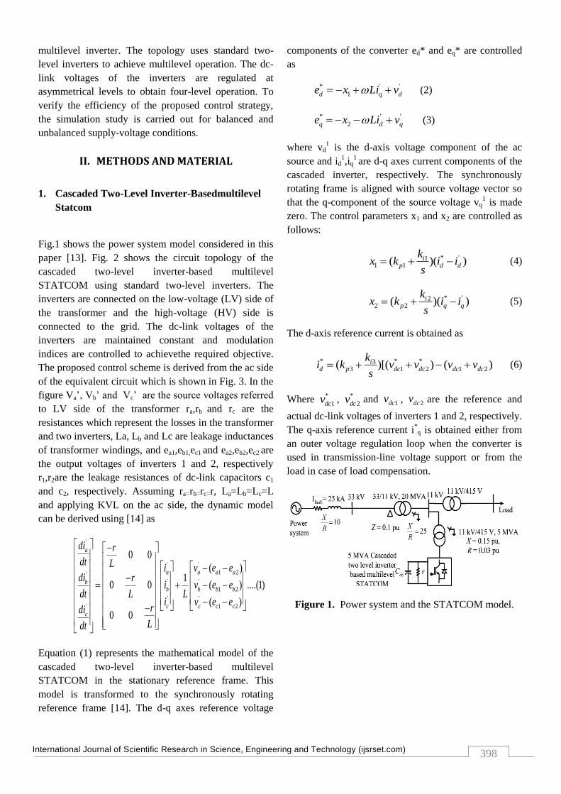
Fig.1 shows the power system model considered in this
paper [13]. Fig. 2 shows the circuit topology of the
cascaded two-level inverter-based multilevel
STATCOM using standard two-level inverters. The
inverters are connected on the low-voltage (LV) side of
the transformer and the high-voltage (HV) side is
connected to the grid. The dc-link voltages of the
inverters are maintained constant and modulation
indices are controlled to achievethe required objective.
The proposed control scheme is derived from the ac side
of the equivalent circuit which is shown in Fig. 3. In the
figure Va’, Vb’ and Vc’ are the source voltages referred
to LV side of the transformer ra,rb and rc are the
resistances which represent the losses in the transformer
and two inverters, La, Lb and Lc are leakage inductances
of transformer windings, and ea1,eb1,ec1 and ea2,eb2,ec2 are
the output voltages of inverters 1 and 2, respectively
r1,r2are the leakage resistances of dc-link capacitors c1
and c2, respectively. Assuming ra=rb=rc=r, La=Lb=Lc=L
and applying KVL on the ac side, the dynamic model
can be derived using [14] as
'
' '
1 2'' '
1 2
' '
' 1 2
0 0
( )1
0 0 ( ) ....(1)
( )
0 0
a
a a a a
bb b b b
c c c c
c
di r
dt L i v e edi r
i v e edt L L
i v e erdi
Ldt
Equation (1) represents the mathematical model of the
cascaded two-level inverter-based multilevel
STATCOM in the stationary reference frame. This
model is transformed to the synchronously rotating
reference frame [14]. The d-q axes reference voltage
components of the converter ed* and eq* are controlled
as
* ' '
1d q de x Li v (2)
* ' '
2q d qe x Li v (3)
where vd1 is the d-axis voltage component of the ac
source and id1,iq
1 are d-q axes current components of the
cascaded inverter, respectively. The synchronously
rotating frame is aligned with source voltage vector so
that the q-component of the source voltage vq1 is made
zero. The control parameters x1 and x2 are controlled as
follows:
* '11 1( )( )i
p d d
kx k i i
s (4)
* '22 2( )( )i
p q q
kx k i i
s (5)
The d-axis reference current is obtained as
* * *33 1 2 1 2( )[( ) ( )i
d p dc dc dc dc
ki k v v v v
s (6)
Where *
1dcv , *
2dcv and 1dcv , 2dcv are the reference and
actual dc-link voltages of inverters 1 and 2, respectively.
The q-axis reference current i*q is obtained either from
an outer voltage regulation loop when the converter is
used in transmission-line voltage support or from the
load in case of load compensation.
Figure 1. Power system and the STATCOM model.

International Journal of Scientific Research in Science, Engineering and Technology (ijsrset.com) 399
Figure 2. Cascaded two-level inverter-based multilevel
STATCOM
Figure 3. Equivalent circuit of the cascaded two-level
inverter-based multilevel STATCOM.
2. Control Strategy
The control block diagram is shown in Fig.5. The unit
signals cos t and sin t are generated from the
phase-locked loop (PLL) using three-phase supply
voltages (Va,Vb,Vc) [14]. The converter currents
(i’a,i’b,i’c) are transformed to the synchronous rotating
reference frame using the unit signals. The switching
frequency ripple in the converter current components is
eliminated using a low-pass filter (LPF). From
(v*dc1+v*dc2) and iq* loops, the controller generates d-q
axes reference voltages, e*d and e*q for the cascaded
inverter. With these reference voltages, the inverter
supplies the desired reactive current (iq*) and draws
required active current (id*) to regulate total dc-link
voltage v*dc1+v*dc2 . However, this will not ensure that
individual dc-link voltages are controlled at their
respective reference values. Hence, additional control is
required to regulate individual dc-link voltages of the
inverters.
Figure 4. Control algorithm of STATCOM with PI
controller
Figure 5. Control Block Diagram
3. DC-Link Balance Controller
The resulting voltage of the cascaded converter can be
given as ei at an angle δ where 2 2
i d qe e e ,
International Journal of Scientific Research in Science, Engineering and Technology (ijsrset.com) 400
1tanq
d
e
e
.The active power transfer between the
source and inverter depends on δ and is usually small in
the inverters supplying var to the grid [1]. Hence, δ can
be assumed to be proportional to eq. Therefore, the q-
axis reference voltage component of inverter-2 e*q2 is
derived to control the dc-link voltage of inverter-2 as
* * *42 4 1 2( )( )i
q p dc dc
ke k v v
s (7)
The q-axis reference voltage component of inverter-1
e*q1 is obtained as
* * *
1 2q q qe e e (8)
The dc-link voltage of inverter-2 Vdc2 is controlled at
0.366 times the dc-link voltage of inverter-1 Vdc1 [9]. It
results in four-level operation in the output voltage and
improves the harmonic spectrum. Expressing dc-link
voltages of inverter-1 and inverter-2 in terms of total dc-
link voltage, Vdc as
2 0.268dc dcV V (9)
1 0.732dc dcV V (10)
Since the dc-link voltages of the two inverters are
regulated, the reference d-axis voltage component e*d is
divided in between the two inverters in proportion to
their respective dc-link voltage as
* *
1 0.732d de e (11)
* *
2 0.268d de e (12)
For a given power, if Vdc2< V*dc2,
*
21
2 *
2
tanq
d
e
e
increases and
*
11
1 *
1
tanq
d
e
e
decreases. Therefore,
power transfer to inverter-2 increases, while it decreases
for inverter-1. The power transfer to inverter-2 is
directly controlled, while for inverter-1, it is controlled
indirectly. Therefore, during disturbances, the dc-link
voltage of inverter-2 is restored to its reference quickly
compared to that of inverter-1. Using e*d1 and e*q1, the
reference voltages are generated in stationary reference
frame for inverter-1 and using e*d2 and e*q2 for inverter-
2. The reference voltages generated for inverter-2 are in
phase opposition to that of inverter-1. From the
reference voltages, gate signals are generated using the
sinusoidal pulse-width modulation (PWM) technique
[15]. Since the two inverters’ reference voltages are in
phase opposition, the predominant harmonic appears at
double the switching frequency.
4. Unbalanced Conditions
Network voltages are unbalanced due to asymmetric
faults or unbalanced loads [16]. As a result, negative-
sequence voltage appears in the supply voltage. This
causes a double supply frequency component in the dc-
link voltage of the inverter. This double frequency
component injects the third harmonic component in the
ac side [17]. Moreover, due to negative-sequence
voltage, large negative-sequence current flows through
the inverter which may cause the STATCOM to trip
[16]. Therefore, during unbalance, the inverter voltages
are controlled in sucha way that either negative-
sequence current flowing into the inverter is eliminated
or reduces the unbalance in the grid voltage. In the latter
case, STATCOM needs to supply large currents since
the interfacing impedance is small. This may lead to
tripping of the converter. The negative-sequence
reference voltage components of the inverter e*dn and
e*qn are controlled similar to positive-sequence
components in the negative synchronous rotating frame
as
* ' '
3 ( )dn qn dne x L i v (13)
* ' '
3 ( )qn dn qne x L i v (14)
Where v’dn,v’qn are d-q axes negative-sequence voltage
components of the supply and i’dn ,i’qn are d-q axes
negative-sequence current components of the inverter,
respectively. The control parameters x3 and x4 are
controlled as follows:
* '53 5( )( )i
p dn dn
kx k i i
s (15)
* '64 6( )( )i
p qn qn
kx k i i
s (16)
The reference values for negative-sequence current
components i*dn and i*qn are set at zero to block
International Journal of Scientific Research in Science, Engineering and Technology (ijsrset.com) 401
negative-sequence current from flowing through the
inverter.
5. Stability Analysis
Considering the dc side of the two inverters in Fig.3, the
complete dynamics of the system are derived in the
Appendix. The transfer function is as follows:
1 1
1( )( )
dcV s num s
den ss
(17)
2 1
2( )( )
dcV s num s
den ss
(18)
Hence, the poles of transfer function always lie on the
left half of the s-plane. However, numerators of the
transfer functions are functions of the operating
conditions. The positions of zeros primarily dependent.
The sign of these variables changes according to the
mode of operation. Therefore, zeros of the transfer
functions shift to the right half of the s-plane for certain
operating conditions. This system is said to be non-
minimum phase and there is a limit on achievable
dynamic response[19]. The system may exhibit
oscillatory instability when there is a step change in
reference for high controller gains. Therefore, the
controller gains should be designed suitably to avoid the
instability. This behavior is similar to that of the two-
level inverter-based STATCOM.
When STATCOM is in inductive mode of operation.
The reactive component is set at 0.75 p.u. and
proportional gain is varied from 0 to 10. It can be seen
that all poles lie on the left half of the s-plane for this
case as well. However, one zero shift to the right half
and three zeros lie on the left half of the s-plane.
Moreover, it can be seen that closed-loop poles of the
system shift to the right half of the s-plane for high
controller gains.
III. RESULTS AND DISCUSSION
The system configuration shown in Fig.1 is considered
for simulation. The simulation study is carried out using
MATLAB/SIMULINK. The system parameters are
given in Table I.
Table I : Simulation System Parameters
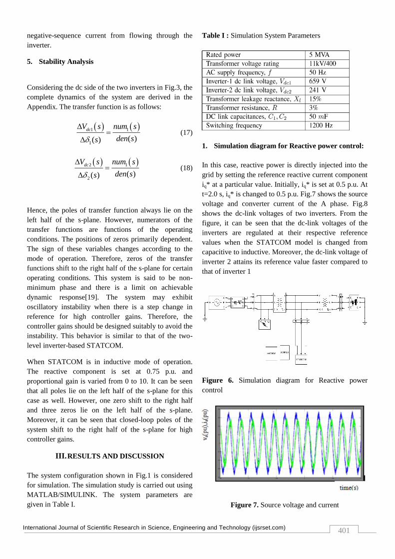
1. Simulation diagram for Reactive power control:
In this case, reactive power is directly injected into the
grid by setting the reference reactive current component
iq* at a particular value. Initially, iq* is set at 0.5 p.u. At
t=2.0 s, iq* is changed to 0.5 p.u. Fig.7 shows the source
voltage and converter current of the A phase. Fig.8
shows the dc-link voltages of two inverters. From the
figure, it can be seen that the dc-link voltages of the
inverters are regulated at their respective reference
values when the STATCOM model is changed from
capacitive to inductive. Moreover, the dc-link voltage of
inverter 2 attains its reference value faster compared to
that of inverter 1
Figure 6. Simulation diagram for Reactive power
control
Figure 7. Source voltage and current
International Journal of Scientific Research in Science, Engineering and Technology (ijsrset.com) 402
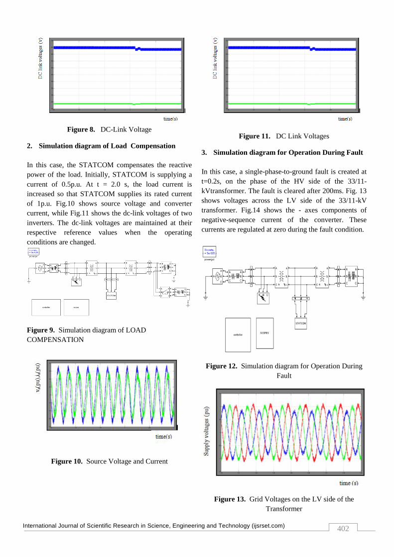
Figure 8. DC-Link Voltage
2. Simulation diagram of Load Compensation
In this case, the STATCOM compensates the reactive
power of the load. Initially, STATCOM is supplying a
current of 0.5p.u. At t = 2.0 s, the load current is
increased so that STATCOM supplies its rated current
of 1p.u. Fig.10 shows source voltage and converter
current, while Fig.11 shows the dc-link voltages of two
inverters. The dc-link voltages are maintained at their
respective reference values when the operating
conditions are changed.
Figure 9. Simulation diagram of LOAD
COMPENSATION
Figure 10. Source Voltage and Current
Figure 11. DC Link Voltages
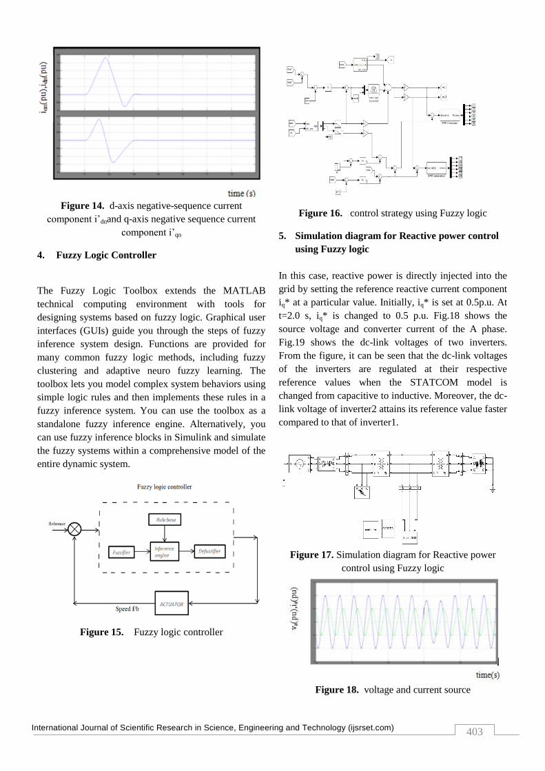
3. Simulation diagram for Operation During Fault
In this case, a single-phase-to-ground fault is created at
t=0.2s, on the phase of the HV side of the 33/11-
kVtransformer. The fault is cleared after 200ms. Fig. 13
shows voltages across the LV side of the 33/11-kV
transformer. Fig.14 shows the - axes components of
negative-sequence current of the converter. These
currents are regulated at zero during the fault condition.
Figure 12. Simulation diagram for Operation During
Fault
Figure 13. Grid Voltages on the LV side of the
Transformer
International Journal of Scientific Research in Science, Engineering and Technology (ijsrset.com) 403
Figure 14. d-axis negative-sequence current
component i’dnand q-axis negative sequence current
component i’qn
4. Fuzzy Logic Controller
The Fuzzy Logic Toolbox extends the MATLAB
technical computing environment with tools for
designing systems based on fuzzy logic. Graphical user
interfaces (GUIs) guide you through the steps of fuzzy
inference system design. Functions are provided for
many common fuzzy logic methods, including fuzzy
clustering and adaptive neuro fuzzy learning. The
toolbox lets you model complex system behaviors using
simple logic rules and then implements these rules in a
fuzzy inference system. You can use the toolbox as a
standalone fuzzy inference engine. Alternatively, you
can use fuzzy inference blocks in Simulink and simulate
the fuzzy systems within a comprehensive model of the
entire dynamic system.
Figure 15. Fuzzy logic controller
Figure 16. control strategy using Fuzzy logic
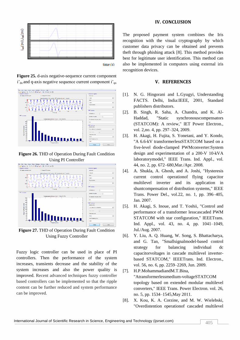
5. Simulation diagram for Reactive power control
using Fuzzy logic
In this case, reactive power is directly injected into the
grid by setting the reference reactive current component
iq* at a particular value. Initially, iq* is set at 0.5p.u. At
t=2.0 s, iq* is changed to 0.5 p.u. Fig.18 shows the
source voltage and converter current of the A phase.
Fig.19 shows the dc-link voltages of two inverters.
From the figure, it can be seen that the dc-link voltages
of the inverters are regulated at their respective
reference values when the STATCOM model is
changed from capacitive to inductive. Moreover, the dc-
link voltage of inverter2 attains its reference value faster
compared to that of inverter1.
Figure 17. Simulation diagram for Reactive power
control using Fuzzy logic
Figure 18. voltage and current source
International Journal of Scientific Research in Science, Engineering and Technology (ijsrset.com) 404
Figure 19. DC link voltages
6. Simulation diagram of Load Compensation
using Fuzzy logic:
In this case, the STATCOM compensates the reactive
power of the load. Initially, STATCOM is supplying a
current of 0.5 p.u. At t = 2.0 s, the load current is
increased so that STATCOM supplies its rated current
of 1 p.u. Fig.21 shows source voltage and converter
current, while Fig.22 shows the dc-link voltages of two
inverters. The dc-link voltages are maintained at their
respective reference values when the operating
conditions are changed.
Figure 20.Simulation diagram of LOAD
COMPENSATION using Fuzzy logic
Figure 21. Source Voltage and Current
Figure 22. DC link Voltages
7. Simulation diagram for Operation During Fault
using Fuzzy logic:
In this case, a single-phase-to-ground fault is created at
t=0.2s, on the phase of the HV side of the 33/11-
kVtransformer. The fault is cleared after 200 ms. Fig.24
shows voltages across the LV side of the 33/11-kV
transformer. Fig.25 shows the d-q axes components of
negative-sequence current of the converter. These
currents are regulated at zero during the fault condition.
Figure 23. Simulation diagram for OPERATION
DURING FAULT using Fuzzy logic
Figure 24. Grid Voltages on the LV side of the
Transformer
International Journal of Scientific Research in Science, Engineering and Technology (ijsrset.com) 405
Figure 25. d-axis negative-sequence current component
i’dn and q-axis negative sequence current component i’qn
Figure 26. THD of Operation During Fault Condition
Using PI Controller
Figure 27. THD of Operation During Fault Condition
Using Fuzzy Controller
Fuzzy logic controller can be used in place of PI
controllers. Then the performance of the system
increases, transients decrease and the stability of the
system increases and also the power quality is
improved. Recent advanced techniques fuzzy controller
based controllers can be implemented so that the ripple
content can be further reduced and system performance
can be improved.
IV. CONCLUSION
The proposed payment system combines the Iris
recognition with the visual cryptography by which
customer data privacy can be obtained and prevents
theft through phishing attack [8]. This method provides
best for legitimate user identification. This method can
also be implemented in computers using external iris
recognition devices.
V. REFERENCES
[1]. N. G. Hingorani and L.Gyugyi, Understanding
FACTS. Delhi, India:IEEE, 2001, Standard
publishers distributors.
[2]. B. Singh, R. Saha, A. Chandra, and K. Al-
Haddad, "Static synchronouscompensators
(STATCOM): A review," IET Power Electron.,
vol. 2,no. 4, pp. 297–324, 2009.
[3]. H. Akagi, H. Fujita, S. Yonetani, and Y. Kondo,
"A 6.6-kV transformerlessSTATCOM based on a
five-level diode-clamped PWMconverter:System
design and experimentation of a 200-V 10-kVA
laboratorymodel," IEEE Trans. Ind. Appl., vol.
44, no. 2, pp. 672–680,Mar./Apr. 2008.
[4]. A. Shukla, A. Ghosh, and A. Joshi, "Hysteresis
current control operationof flying capacitor
multilevel inverter and its application in
shuntcompensation of distribution systems," IEEE
Trans. Power Del., vol.22, no. 1, pp. 396–405,
Jan. 2007.
[5]. H. Akagi, S. Inoue, and T. Yoshii, "Control and
performance of a transformer lesscascaded PWM
STATCOM with star configuration," IEEETrans.
Ind. Appl., vol. 43, no. 4, pp. 1041–1049,
Jul./Aug. 2007.
[6]. Y. Liu, A. Q. Huang, W. Song, S. Bhattacharya,
and G. Tan, "Smallsignalmodel-based control
strategy for balancing individual dc
capacitorvoltages in cascade multilevel inverter-
based STATCOM," IEEETrans. Ind. Electron.,
vol. 56, no. 6, pp. 2259–2269, Jun. 2009.
[7]. H.P.MohammadiandM.T.Bina,
"Atransformerlessmedium-voltageSTATCOM
topology based on extended modular multilevel
converters," IEEE Trans. Power Electron. vol. 26,
no. 5, pp. 1534–1545,May 2011.
[8]. X. Kou, K. A. Corzine, and M. W. Wielebski,
"Overdistention operationof cascaded multilevel
International Journal of Scientific Research in Science, Engineering and Technology (ijsrset.com) 406
inverters," IEEE Trans. Ind. Appl., vol. 42,no. 3,
pp. 817–824, May/Jun. 2006.
[9]. K. K. Mohaptra, K. Gopakumar, and V. T.
Somasekhar, "A harmonicelimination and
suppression scheme for an open-end winding
inductionmotor drive," IEEE Trans. Ind.
Electron., vol. 50, no. 6, pp. 1187–1198,Dec.
2003.
[10]. Y. Kawabata, N. Yahata,M. Horii, E. Egiogu, and
T. Kawabata, "SVGusing open winding
transformer and two inverters," in Proc., 35th
AnnualIEEE Power Electron. Specialists Conf.,
2004, pp. 3039–3044.
[11]. S. Ponnaluri, J. K. Steinke, P. Steimer, S.
Reichert, and B. Buchmann,"Design comparison
and control of medium voltage STATCOM
withnovel twin converter topology," in Proc., 35th
Annu. IEEE Power Electron.Specialists Conf.,
2004, pp. 2546–2550.
[12]. N. N. V. Surendra Babu, D. Apparao, and B. G.
Fernandes, "Asymmetricaldc link voltage balance
of a cascaded two level inverter
basedSTATCOM," in Proc., IEEE TENCON,
2010, pp. 483–488.
[13]. IEEE Criteria for Class IE Electric Systems, IEEE
Standard 141-1993.
[14]. C. Schauder and H. Mehta, "Vector analysis and
control of advancedstatic VAr compensators," in
Proc. Inst. Elect. Eng. C., Jul. 1993, vol.140, no.
4, pp. 299–305.
[15]. D. G. Holmes and T. A. Lipo, "IEEE series on
power engineering," inPulse Width Modulation
for Power Converters: Principles and
Practice.Piscataway, NJ, USA: IEEE, 2003.
[16]. B. Blazic and I. Papic, "Improved D-statcom
control for operation withunbalanced currents and
voltages," IEEE Trans. Power Del., vol. 21,no. 1,
pp. 225–233, Jan. 2006.
[17]. A. Leon, J.M.Mauricio, J. A. Solsona, and A.
Gomez-Exposito, "Softwaresensor-based
STATCOM control under unbalanced
conditions,"IEEE Trans. Power Del., vol. 24, no.
3, pp. 1623–1632, Jul. 2009.
[18]. Y. Suh, Y. Go, and D. Rho, "A comparative study
on control algorithmfor active front-end rectifier
of large motor drives under unbalancedinput,"
IEEE Trans. Ind. Appl., vol. 47, no. 3, pp. 825–
835, May/Jun.2011.
[19]. K. Ogata, Modern Control Engineering, 4th ed.
Delhi, India:Pearson, 2004.
[20]. K. R. Padiyar and A. M. Kulkarni, "Design of
reactive current andvoltage controller of static
condenser," Elect. Power Energy Syst., vol.19, no.
6, pp. 397–410, 1997.SI/IEEE, 1997.

![Advance In Micromechanics Analysis of Piezoelectric …ijsrset.com/paper/1587.pdf · theories of piezoelectric shells. Qin [8-11] discussed Green’s functions, advanced theory, and](https://static.fdocuments.in/doc/165x107/5b0468d47f8b9a4e538daf7e/advance-in-micromechanics-analysis-of-piezoelectric-of-piezoelectric-shells.jpg)