Carrier Dynamics in the Nitride Semiconductors · Carrier Dynamics in the Nitride Semiconductors A...
97
UNIVERSITY OF CALIFORNIA Santa Barbara Carrier Dynamics in the Nitride Semiconductors A Dissertation submitted in partial satisfaction of the requirements for the degree Doctor of Philosophy in Electrical and Computer Engineering Kian-Giap Gan Committee: Professor John E. Bowers, Chair Professor Chi-Kuang Sun Professor Steven P. DenBaars Professor Shuji Nakamura Professor David D. Awschalom December, 2006
Transcript of Carrier Dynamics in the Nitride Semiconductors · Carrier Dynamics in the Nitride Semiconductors A...

UNIVERSITY OF CALIFORNIA Santa Barbara
Carrier Dynamics in the Nitride Semiconductors
A Dissertation submitted in partial satisfaction of the requirements for the degree Doctor of Philosophy in
Electrical and Computer Engineering
Kian-Giap Gan
Committee:
Professor John E. Bowers, Chair Professor Chi-Kuang Sun
Professor Steven P. DenBaars Professor Shuji Nakamura
Professor David D. Awschalom
December, 2006
The dissertation of Kian-Giap Gan is approved
Chi-Kuang Sun
Steven P. DenBaars
Shuji Nakamura
David D. Awschalom
John E. Bowers, Chair
Dec, 2006

Carrier Dynamics in the Nitride Semiconductors
Copyright © 2006 by Kian-Giap Gan All right reserved
Electrical and Computer Engineering Department University of California
Santa Barbara, CA 93106
iii

Acknowledgements
Acknowledgements
iv
I will always remember my time at UCSB, not only because the beautiful
scenery and the gorgeous weather, but also because of the wonderful experience
I have had and the wonderful people I have met.
First of all, I would like to express my deepest appreciation to my
advisor, Professor John Bowers, for provided a stimulating environment with
total academic freedom and allowed me to choose my own research direction.
Along the way, he has been supportive, providing guidance and mentorship and
the funding that the project required. My Ph.D. committee has helped shape and
guides the scope of this work and I thank them for their contribution: Professors
Chi-Kuang Sun, Steve P. DenBaars, Shuji Nakamura, and David D. Awschalom.
I would like to thank Arpan and Rajat for providing me the InGaN thin
films sample that was used in the measurement. I also want to thanks Professor
Claude Weisbush for collaboration and discussion on the study of the carrier
transport dynamics in the InGaN thin films sample.
Finally, I would like to thank my parents for always supporting and
encouraging me throughout the course of my life.

Acknowledgements
v
This dissertation is dedicated
to my family

Curriculum Vitæ
Curriculum Vitæ
vi
Kian-Giap Gan
Employment
1999-2005 Graduate Student Researchers Professor John Bowers, University of California, Santa Barbara, California, USA
1998-1999 Undergraduate Student Research Assistant
Professor Chi-Kuang Sun, National Taiwan University, Taipei, Taiwan
Education
2001-2006 Ph.D. in Electrical and Computer Engineering Professor John Bowers, University of California, Santa Barbara, California, USA.
1999-2001 M.S. in Electrical Engineering
Professor John Bowers, University of California, Santa Barbara, California, USA.
1995-1999 B.S. in Electrical Engineering
National Taiwan University, Taipei, Taiwan.
Awards

Curriculum Vitæ
vii
2004 Walsin Fellowship 1994 First place in the Malaysia National Mathematics Competition 1993 Third place in the Malaysian Mathematical Olympiad

Publications
Publications
viii
First-author journal papers
Kian-Giap Gan, Chi-Kuang Sun, Steven P. DenBaars, and John E. Bowers, “Ultrafast hole intervalence subband relaxation in an InGaN multiple quantum well laser diode,” Applied Physics Letters, 80, pp. 4054-4056, 2002.
Kian-Giap Gan, and John E. Bowers, “Measurements of Gain, Group index, and Linewidth Enhancement Factor of an InGaN Multiple Quantum Well Laser Diode,” IEEE Photonics Technology Letters, 16, pp. 1256-1258, 2004.
Kian-Giap Gan, Jin-Wei Shi, Yen-Hung Chen, Chi-Kuang Sun, Yi-Jen Chiu, and John E. Bowers, “Ultrahigh power-bandwidth-product performance of low-temperature-grown-GaAs based metal-semiconductor-metal traveling-wave photodetectors,” Applied Physics Letters, 80, pp. 4054-4056, May 2002.
First-author conference papers
Kian-Giap Gan, J. E. Bowers, and Chi-Kuang Sun, “Femtosecond carrier dynamics in InGaN multiple-quantum-well laser diodes under high injection levels,” in Proceedings of the 17th Annual Meeting of the IEEE Lasers and Electro-Optics Society, Vol.2, Puerto Rico, 2004, pp. 669-670.
Kian-Giap Gan, Chi-Kuang Sun, John E. Bowers, and Steven P. DenBaars, “Ultrafast carrier dynamics in InGaN MQW laser diode,” in Proceedings of SPIE Vol.4992 Ultrafast Phenomena in Semiconductors VII, 2003, pp. 83-89. (invited)

Publications
ix
Kian-Giap Gan, John E. Bowers, Steven P. DenBaars, and Chi-Kuang Sun, “Ultrafast inter-subband hole relaxation in an InGaN multiple-quantum-well (MQW) laser diode,” in Ultrafast Electronics and Optoelectronics, 2003, pp. 38-41.
Kian-Giap Gan, Jin-Wei Shi, Yi -Jen Chiu, Chi-Kuang Sun, and J. E. Bowers, “Self-aligned MSM low-temperature-grown GaAs traveling wave photodetector for 810 nm and 1230 nm,”. International Topical Meeting on Microwave Photonics 2001, paper Tu-4.15, pp. 153-155, Long Beach, California, January 7-9 (2002).
Kian-Giap Gan, Jin-Wei Shi, Yi-Jen Chiu, Chi-Kuang Sun, and John E. Bowers, “Self-Aligned 0.8ps FWHM MSM Traveling Wave Photodetector Using Low-Temperature-Grown GaAs,” in Ultrafast Electronics and Optoelectronics, 2001, pp. 114-116.
Coauthored papers and presentations
J. Geske, K.-G. Gan, Y. L. Okuno, J. Piprek, and J. E. Bowers, “Vertical-cavity surface-emitting laser active regions for enhanced performance with optical pumping,”, IEEE Journal of Quantum Electronics, 40, pp. 1155-1162, 2004.
J. Geske, K.-G. Gan, Y. L. Okuno, B. Barnes, J. Piprek, and J. E. Bowers, “Vertical-cavity surface-emitting laser active regions for enhanced performance with optical pumping,” in Proceedings of the Conference on Lasers and Electro Optics, 2004, pp. 815-816.
D. Lasaosa, Jin-Wei Shi, D. Pasquariello, Kian-Giap Gan, Ming-Chun Tien, Hsu-Hao Chang, Shi-Wei Chu, Chi-Kuang Sun, Yi-Jen Chiu, and J. E. Bowers, “Traveling-wave photodetectors with high power-bandwidth and gain-bandwidth product performance,” IEEE Journal of Select Topics in Quantum Electronics, 10, pp. 728-741, 2004.

Publications
x
Jin-Wei Shi, Yen-Hung Chen, Kian-Giap Gan, Yi-Jen Chiu, John E. Bowers, Ming-Chun Tien, Tzu-Ming Liu, and Chi-Kuang Sun, “Nonlinear Behaviors of Low-Temperature-Grown GaAs-Based Photodetectors Around 1.3-µm Telecommunication Wavelength,” IEEE Photonics Technology Letters, 16, pp. 242-244, 2004.
Yae Okuno, Jonathan Geske, Kian-Giap Gan, Yi-Jen Chiu, Steven P. DenBaars, and John E. Bowers, “1.3 µm wavelength vertical cavity surface emitting laser fabricated by orientation-mismatched wafer bonding: A prospect for polarization control,” Applied Physics Letters, 82, pp. 2377-2379, 2003.
Jin-Wei Shi, Kian-Giap Gan, Yen-Hung Chen, Chi-Kuang Sun, Yi-Jen Chiu, and J. E. Bowers, “Ultrahigh-power-bandwidth product and nonlinear photoconductance performances of low-temperature-grown GaAs-based metal-semiconductor-metal traveling-wave photodetectors,” IEEE Photonics Technology Letters, 14, pp. 1587-1589, 2002.
Jin-Wei Shi, Yen-Hung Chen, Kian-Giap Gan, Yi-Jen Chiu, Chi-Kuang Sun, and J. E. Bowers, “High-speed and high-power performances of LTG-GaAs based metal-semiconductor-metal traveling-wave-photodetectors in 1.3-µm wavelength regime,” IEEE Photonics Technology Letters, 14, pp. 363-365, 2002.
Jin-Wei Shi, Kian-Giap Gan, Yi-Jen Chiu, Yen-Hung Chen, Chi-Kuang Sun, Ying-Jay Yang, and J. E. Bowers, “Metal-semiconductor-metal traveling-wave photodetectors,” IEEE Photonics Technology Letters, 13, pp. 623-625, 2001.
Jin-Wei Shi, Kian-Giap Gan, Yi-Jen Chiu, J. E. Bowers, and Chi-Kuang Sun, “High power performance of ultrahigh bandwidth MSM TWPDs,” in Proceedings of the 14th Annual Meeting of the IEEE Lasers and Electro-Optics Society, Vol.2, Piscataway, NJ, 2001, pp. 887-888. Jin-Wei Shi, Kian-Giap Gan, Yi-Jen Chiu, Chi-Kuang Sun, Yin-Jay Yang, and J. E. Bowers, “Ultrahigh bandwidth MSM traveling-wave photodetectors,” in Proceedings of the Conference on Lasers and Electro Optics, 2001, pp. 348.

Abstract
Abstract
Carrier Dynamics in the Nitride Semiconductor
by
Kian-Giap Gan
The group-III nitride semiconductor alloys AlN-GaN-InN are recognized as an
important material system for optoelectronic devices in the spectral range from
infrared to ultraviolet. This thesis will investigate the carrier relaxation and
carrier transport dynamics in InGaN, which are important for high speed device
design.
Time-resolved pump-probe measurement is used to study carrier
relaxation dynamics in an InGaN multiple-quantum-well (MQW) laser diode.
Using the optical selection rule in InGaN, different subbands can be selectively
pumped and probed using ultrafast optical pulse with different polarization. An
ultrafast intersubband relaxation process ( <0.35 ps) is found to be important to
carrier dynamics in InGaN.
τ
A novel heterodyne transient grating measurement is developed and used
to study the carrier transport dynamics in InGaN. The measured diffusion
xi

Abstract
xii
constant is very small (~0.2 cm2/s), indicate that carrier localization plays an
important role in the carrier transport in InGaN MQWs. A simple model is
presented to explain the measurement result.

Table of Contents
Table of Contents
xiii
Chapter 1. Introduction......................................1
1.1 Motivation ................................................................1
1.2 Organization of dissertation......................................2
1.3 Reference ..................................................................3
Chapter 2. Gain in nitride semiconductor laser
diodes ............................................................5
2.1 Fourier Transform (FT) method ...............................7
2.1.1 Calculation of net modal gain............................................ 9
2.1.2 Calculation of group index and group velocity
dispersion ........................................................................... 9
2.1.3 Calculation of linewidth enhancement factor.................. 10
2.1.4 Calculation of temperature-induced index change.......... 12
2.2 Measurement results of InGaN MQW laser diode .13
2.2.1 Measurement of gain........................................................ 16
2.2.2 Measurement of group index and group velocity
dispersion ......................................................................... 17
2.2.3 Measurement of linewidth enhancement factor ............... 18
2.2.4 Measurement of thermal-induced index change.............. 21

Table of Contents
xiv
2.3 Summary.................................................................23
2.4 References ..............................................................24
Chapter 3. Intervalence subband carrier
dynamics in InGaN MQW laser diodes ...............26
3.1 Introduction ............................................................26
3.2 Band structure and optical selection rule for
InGaN .....................................................................28
3.3 Bias lead monitoring measurement ........................35
3.4 Time-resolved differential reflection measurement 40
3.4.1 Determination of transparency level ............................... 44
3.4.2 Intersubband relaxation under high carrier density........ 46
3.5 Summary and future work ......................................49
3.6 Reference ................................................................51
Chapter 4. Diffusion constant of InGaN MQW
thin films ..........................................................53
4.1 Conventional transient grating measurement .........54
4.2 New heterdodyne transient grating measurement...57
4.3 Important optical alignment issue...........................63

Table of Contents
xv
4.4 Validation of the new heterodyne transient grating
method ....................................................................65
4.5 Diffusion constant of InGaN MQW .......................67
4.6 Diffusion model......................................................73
4.7 Summary and future work ......................................77
4.8 Reference ................................................................78
Chapter 5. Summary and future work............79
5.1 Gain measurement ..................................................79
5.2 Valence intersubband relaxation.............................79
5.3 Carrier transport in InGaN......................................80
5.4 Reference ................................................................81

Chapter 1. Introduction
Chapter 1. Introduction
The group-III nitride semiconductor alloys AlN-GaN-InN are recognized as an
important material system for optoelectronic devices in the spectral range from
infrared to ultraviolet. GaN-InN based III-V nitride semiconductors are of
interest in many commercial applications, such as light emitting diodes (LEDs)
and laser diodes (LDs) [1, 2].
1.1 Motivation
The carrier dynamics, which are important for high speed device design, have
recently been studied by femtosecond time-resolved pump-probe [3] or coherent
spectroscopy [4, 5] with above band gap photons. However, various
contributions such as electron-electron scattering, hole-hole scattering, electron-
hole scattering, electron-phonon interactions, and hole-phonon interactions, mix
together and make it very difficult to extract the fundamental material parameter
for one particular scattering process or single type of carrier. C.-K. Sun et al.
and H. Ye et al. have developed an infrared pump-ultraviolet probe technique to
1

Chapter 1. Introduction
isolate electron and hole dynamics and used it to study the electron relaxation
dynamics in n-type GaN thin films [6, 7] and hole dynamics in p-type GaN thin
films [8]. In this thesis, we will use the optical selection in the InGaN quantum
well to selectively pump and probe different subbands, and this allows us to
study specifically the relaxation of carrier among various subbands in the
valence band.
It is well known that nitrides have strong internal electric fields due to
the spontaneous polarization and piezo-electric effect [9]. K. Omae et al. have
used pump-probe spectroscopy to study the effects of internal electrical field on
the transient absorption in InxGa1-xN quantum well thin films with different
thickness [10]. The effect of the internal electric fields will be included in the
calculation and explanation for the data.
1.2 Organization of dissertation
The dissertation will start by the measurement of the gain spectrum, group
velocity dispersion, and other interesting parameters in an InGaN multiple-
quantum-well (MQW) laser diode with the Fourier transform method in Chapter
2. In Chapter 3, time-resolved pump-probe measurement is used to study the
carrier relaxation dynamic in an InGaN multiple-quantum-well (MQW) laser
diode. Using the optical selection rule in InGaN, difference subbands can be
2

Chapter 1. Introduction
selectively pump and probe using ultrafast optical pulse with difference
polarization. An ultrafast intersubband relaxation process (τ <0.35 ps) is found
to be important to carrier dynamics in InGaN. In Chapter 4, a novel heterodyne
transient grating measurement is developed and used to study the carrier
transport dynamics in InGaN. The measured diffusion constant is very small
(~0.2 cm2/s), indicate that carrier localization plays an important role in the
carrier transport in the InGaN MQW. A simple model is presented to explain
the measurement result.
1.3 Reference [1] S. Nakamura, M. Senoh, and T. Mukai, "High-power InGaN/GaN
double-heterostructure violet light emitting diodes," Applied Physics Letters, vol. 62, pp. 2390-2392, 1993.
[2] S. Nakamura, M. Senoh, S.-i. Nagahama, N. Iwasa, T. Yamada, T. Matsushita, H. Kiyoku, Y. Sugimoto, T. Kozaki, H. Umemoto, M. Sano, and K. Chocho, "InGaN/GaN/AlGaN-based laser diodes with modulation-doped strained-layer superlattices grown on an epitaxially laterally overgrown GaN substrate," Applied Physics Letters, vol. 72, pp. 211-213, 1998.
[3] C. K. Sun, F. Vallee, S. Keller, J. E. Bowers, and S. P. DenBaars, "Femtosecond studies of carrier dynamics in InGaN," Applied Physics Letters, vol. 70, pp. 2004-2006, 1997.
[4] S. Pau, J. Kuhl, F. Scholz, V. Haerle, M. A. Khan, and C. J. Sun, "Femtosecond degenerate four-wave mixing of GaN on sapphire: Measurement of intrinsic exciton dephasing time," Physical Review B, vol. 56, pp. R12718, 1997.
[5] R. Zimmermann, A. Euteneuer, J. Mobius, D. Weber, M. R. Hofmann, W. W. Ruhle, E. O. Gobel, B. K. Meyer, H. Amano, and I. Akasaki, "Transient four-wave-mixing spectroscopy on gallium nitride: Energy splittings of intrinsic excitonic resonances," Physical Review B, vol. 56, pp. R12722, 1997.
3

Chapter 1. Introduction
[6] C. K. Sun, Y. L. Huang, S. Keller, U. K. Mishra, and S. P. DenBaars, "Ultrafast electron dynamics study of GaN," Physical Review B, vol. 59, pp. 13535, 1999.
[7] H. Ye, G. W. Wicks, and P. M. Fauchet, "Hot electron relaxation time in GaN," Applied Physics Letters, vol. 74, pp. 711-713, 1999.
[8] H. Ye, G. W. Wicks, and P. M. Fauchet, "Hot hole relaxation dynamics in p-GaN," Applied Physics Letters, vol. 77, pp. 1185-1187, 2000.
[9] S. Nakamura and S. F. Chichibu, Introduction to Nitride Semiconductor Blue Lasers and Light Emitting Diodes. New York: Taylor & Francis, 2000.
[10] K. Omae, Y. Kawakami, S. Fujita, Y. Narukawa, and T. Mukai, "Effects of internal electrical field on transient absorption in InxGa1-xN thin layers and quantum wells with different thickness by pump and probe spectroscopy," Physical Review B (Condensed Matter and Materials Physics), vol. 68, pp. 085303-5, 2003.
4

Chapter 2. Gain in nitride semiconductor laser diode
Chapter 2. Gain in nitride semiconductor laser diodes
The measurement of gain (absorption) spectra is an important material
characterization tool for the development of semiconductor lasers,
semiconductor optical amplifiers, and other waveguide devices. A number of
different methods have been proposed to determine the net gain spectrum from
transmission spectra or spontaneous emission spectra. Among the many ways of
measuring net gain spectrum, Hakki-Poali (HP) method is well known for it’s
accuracy, versatility and simplicity [1, 2]. Beside the gain spectrum, HP method
can also be use to deduce information on the refractive index such as carrier-
induced index change ( ) by observing the wavelength shift of Fabry-
Perot resonance [3]. In the HP method, a series of peaks and valleys of
individual Fabry-Perot resonances is recorded, and the gain spectrum can be
calculated from the peak-to-valley ratio. In order to accurately measure the
peak-to-valley ratio, the resolution bandwidth of the measurement instrument
has to be high enough to resolve the Fabry-Perot mode in the measured
spectrum. If the instrument’s resolution bandwidth is not enough to resolve the
/dn dN
5

Chapter 2. Gain in nitride semiconductor laser diode
Fabry-Perot mode, then the measured peak (valley) will be lower (higher) than
the actual peak (valley). These will cause the peak-to-valley ratio to be under
estimated and result in an under estimation of the gain. The instrument
resolution limitation is particular acute when the laser diode is biased close to
the threshold. As the biases of the laser diode approached threshold, the peak-
to-valley ratio will approach infinity, and it becomes increasingly difficult to get
a good measure of the peak-to-valley ratio under this situation. There have been
some papers that aim to alleviate the resolution requirement of the HP method
[4-6]. Most of the research in this area involved the assumption of the shape of
the instrument response function that may not be satisfied by the experiment
conditions. Recently, Hofstetter and Thornton proposed a technique that using
Fourier Transform (FT) analysis on the measured spectrum to obtain the gain
spectrum [7]. In contrast with the HP method, FT method allows the instrument
response correction if the instrument response function can be measured [8]. As
a result, the requirement of the high wavelength resolution of the measurement
instrument can be relaxed. This makes the FT method more suitable for the gain
spectrum measurement on nitride waveguide structure than the HP method.
This is because the emission wavelength of the nitride is shorter and thus has a
smaller Fabry-Perot mode spacing and is more difficult to resolve. On top of the
measured instrument response calibration capability, the FT method is also less
sensitive to the noise in the measured spectrum [8]. Just aas with HP method,
6

Chapter 2. Gain in nitride semiconductor laser diode
information about the refractive index of the measured waveguide can also be
obtained using the FT method [9]. In this chapter, we are going to focus on the
FT method. First, we will show how to use the FT method to calculate the
physical parameter of interest; namely, gain, group index ( ), group velocity
dispersion (GVD), carrier-induced index change ( ), linewidth
enhancement factor (α ) and thermal-induced index change ( ). Then we
will apply the equations that we derived in session 2.1 to the measurement of an
InGaN multiple-quantum-well (MQW) laser diode.
gn
/dn dN
/dn dT
2.1 Fourier Transform (FT) method
We start with the calculation of the gain-reflectivity product (b ) and the round
trip phase ( ) from the measured spontaneous emission spectrum [8,
10]. Where is the wavenumber ( is wavelength). Let us assume
that be the measured instrument response function. Define the Fourier
transform pair as
φ ( )ASES β
1/β = λ λ
( )INSF β
2
2
( ) ( )
( ) ( )
j z
j z
H H z e
H z H e d
+∞+ πβ
−∞+∞
− πβ
−∞
β =
= β
∫
∫
dz
β
<2-1>
7

Chapter 2. Gain in nitride semiconductor laser diode
First, take the Fourier transform of the measured spontaneous emission spectrum
and the Fourier transform of the measured instrument response function. ( )ASES β
2( ) ( ) j zASE ASES z S e d
+∞− πβ
−∞
= β∫ β <2-2>
2( ) ( ) j zINS INSF z F e d
+∞− πβ
−∞
= β∫ β <2-3>
The gain reflectivity product and the round trip phase can be calculated by
32
2
( )( )
( )( )( )
nLASE j z
INSnLnL
ASE j z
INSnL
S ze dz
F zb
S ze dz
F z
++ πβ
++
+ πβ
−
β =∫
∫ <2-4>
32
2
( )( )
( )( )( )
nLASE j z
INSnLnL
ASE j z
INSnL
S ze dz
F z
S ze dz
F z
++ πβ
++
+ πβ
−
⎛ ⎞⎟⎜ ⎟⎜ ⎟⎜ ⎟⎜ ⎟⎜ ⎟φ β = ⎜ ⎟⎜ ⎟⎟⎜ ⎟⎜ ⎟⎜ ⎟⎜ ⎟⎜⎝ ⎠
∫
∫ <2-5>
The gain-reflectivity product (b ) is related to the net modal gain (g ) by
= ⋅ ⋅ ⋅1 2 exp( )b R R g L <2-6>
and the round trip phase (φ ) is related to the refractive index (n ) as
<2-7> φ π β= ⋅ ⋅ ⋅ ⋅ − 04 n L φ
8

Chapter 2. Gain in nitride semiconductor laser diode
where and are the power reflectivity of the front and back facet, g is the
net modal gain, L is the cavity length, is the wavenumber, n is the
effective refractive index, and φ is an unknown phase constant [10].
1R 2R
1/β = λ
0
2.1.1 Calculation of net modal gain
From the gain-reflectivity product (b ), the net modal gain can be calculated as
= ⋅ − ⋅ ⋅⋅ 1 2
1 1ln( ) ln( )
2g b RL L
R . <2-8>
The net modal gain can be calculated if the values of the facet reflectivity and
cavity length are known.
2.1.2 Calculation of group index and group velocity dispersion
The refractive index n cannot be calculated directly from <2-7>, because the
value of is unknown, unless can be determined by using one known
index within the measured spectra range [10]. Fortunately, without knowing the
value of , some important parameters of interest can still be calculated from
<2-7>. For example, the first derivative of <2-7> can be used to calculated the
group index as
0φ 0φ
0φ
9

Chapter 2. Gain in nitride semiconductor laser diode
φβ
β π= + ⋅ = ⋅
⋅ ⋅g
14
dn dn n
d L βd. <2-9>
And the second derivative of <2-7> can be used to calculate the GVD as
βλ π
−≡ = ⋅
⋅ ⋅
2 2g
2GVD4
dn dd L
φβd
dI
. <2-10>
2.1.3 Calculation of linewidth enhancement factor
If a series of spontaneous emission spectra can be measured under several
different injection current (I ) levels and the step of the current level change are
kept small enough so that the induced Fabry-Perot mode shift is smaller than
one mode spacing, then the linewidth enhancement factor can be calculated with
the following procedure.
First, the gain (g ) and round trip phase ( ) at different injection current
levels are calculated as shown previously. The next step is to calculate the
derivative of the gain with respect to the current ( ) and the derivative of
the round trip phase with respect to the current ( ) from the calculation
results of the first step. The derivative of the index with respect to the current
( ) is related to by
φ
/dg dI
/d dIφ
/dn dI /dφ
φπ β
=⋅ ⋅ ⋅
14
dn ddI L dI
⋅ . <2-11>
10

Chapter 2. Gain in nitride semiconductor laser diode
Although the facet reflectivity does change as the current injection levels change
due to the carrier-induced refractive index change, is dominated by the
change of the first term in <2-8>. The carrier-induced reflectivity change is
small compared with the first term in <2-8> because the carrier-induced index
change is very small; unless the facet reflectivity is very low (antireflection-
coated facet). So can be calculated by neglecting the carrier-induced
reflectivity change as
/dg dI
/dg dI
= ⋅1 ln(dg d b
dI L dI) . <2-12>
The linewidth enhancement factor (α ) can be calculated with [11]
πα
λ λ⋅ ⋅
= − ⋅ = − ⋅4 4 dn
dIdgdI
dndg
π . <2-13>
From <2-11>, <2-12>, and <2-13>
φ
α = − ln( )
ddId bdI
<2-14>
It is interesting to point out that the linewidth enhancement factor can be
calculated in this way without knowing the cavity length.
Since the carrier density ( ) can be related to the injection current (I )
by [11]
N
2 3i
a life
I NA N B N C N
q V⋅ = ⋅ + ⋅ + ⋅ =
⋅η
τ <2-15>
11

Chapter 2. Gain in nitride semiconductor laser diode
where η is the injection efficiency, q is the charge of an electron, and is the
active volume of the laser diode, A is the non-radioactive recombination rate,
is carrier life time, B is the bi-molecular recombination coefficient, and C
is the Auger recombination coefficient. The derivative is given by
i aV
τlife
/dI dN
2a a
i i life,
( 2 3 )dI q V q V N
A B N C NdN ∆
⋅ ⋅= ⋅ + ⋅ ⋅ + ⋅ ⋅ = ⋅
η η τ <2-16>
Where is the differential carrier life time. life,∆τ
So the differential gain ( ) and carrier-induced index change ( )
can be calculated as
/dg dN /dn dN
1 ln(dg dI dg dI d bdN dN dI dN L dI
= ⋅ = ⋅ ⋅) <2-17>
14
dn dI dn dI ddN dN dI dN L dI
φπ β
= ⋅ = ⋅ ⋅⋅ ⋅ ⋅
<2-18>
2.1.4 Calculation of temperature-induced index change
Similar to the previous analysis of the carrier-induced index change, if a series
of spontaneous emission spectra can be measured under several different
temperatures (T ) at a fixed injection current level, then the thermal-induced
index change can be calculated as show below. Again, the step of the
12

Chapter 2. Gain in nitride semiconductor laser diode
temperature change needs to be kept small enough so that the temperature-
induced Fabry-Perot mode shift is smaller than one mode spacing.
φα
π β+ ⋅ = ⋅
⋅ ⋅ ⋅thermal
14
dn dn
dT L dT <2-19>
The second term on the left-hand-side of <2-19> is due to the thermal expansion
of the cavity length. As will be shown in the next session, this thermal
expansion term is an order of magnitude smaller than and can be
neglected.
/dn dT
2.2 Measurement results of InGaN MQW laser diode
The schematic diagram of the measurement setup is shown in Figure 2-2. The
polarization-resolved spontaneous emission spectrum from an InGaN multiple-
quantum-well (MQW) blue laser diode is collected using a high-resolution
grating spectrometer (SPEX, 0.5-m focal length, 1200 lines/mm grating, 10-µm
slit width) operated at the second order (~ 0.02-nm resolution bandwidth). The
grating installed in our spectrometer has very low diffraction efficiency for the
transverse-magnetic (TM) polarization. Due to this limitation, we limited the
measurement to the transverse-electric (TE) polarization. The laser diode was
mounted on a temperature controlled stage in order to maintain constant
temperature (20 °C). All the spontaneous emission spectra were measured
13
Chapter 2. Gain in nitride semiconductor laser diode
under pulsed operation in order to avoid heating due to current injection. The
properties of the blue laser diode are summarized as following: lasing
wavelength = 403.5 nm, threshold current = 33 mA, and cavity length = 670 µm.
The laser diode we used in this measurement is a commercial device and the
structure of the laser diode is very similar to the one in [12] and is shown in
Figure 2-1. The In0.15Ga0.85N/In0.02Ga0.98N MQW structure consisting of four 3.5
nm Si-doped In0.15Ga0.85N well layers forming a gain medium separated by 10.5
nm Si-doped In0.02Ga0.98N barrier layers. The measured wavelength range of the
spontaneous emission spectrum of 395-415 nm is chosen (an example of
measured spectrum is shown in Figure 2-3) so that the values of the emission
spectrum at both ends of the measured wavelength range are about the same and
small in order to reduce the spectrum leakage when performing the FT method.
No window function was used in the FT method. The instrument response
deconvolutions were performed with a measured response function [8, 10].
14

Chapter 2. Gain in nitride semiconductor laser diode
(0001) Al2O3 substrateGaN buffer layer
n-electrode
SiO2n-GaN
n-In0.1Ga0.9N
n-Al0.14Ga0.86N/GaN MD-SLSn-GaN
In0.02Ga0.98N/In0.15Ga0.85N MQWp-Al0.2Ga0.8N
p-GaNp-Al0.14Ga0.86N/GaN MD-SLS
p-GaN
p-electrode
(0001) Al2O3 substrateGaN buffer layer
n-electrode
SiO2n-GaN
n-In0.1Ga0.9N
n-Al0.14Ga0.86N/GaN MD-SLSn-GaN
In0.02Ga0.98N/In0.15Ga0.85N MQWp-Al0.2Ga0.8N
p-GaNp-Al0.14Ga0.86N/GaN MD-SLS
p-GaN
p-electrode
Figure 2-1 Schematic diagram of the structure of the InGaN MQW laser diode
Lens
Polarizer
Laser diode
Temperature controlled stage
Spectrometer
LensLens
Polarizer
Laser diode
Temperature controlled stage
Spectrometer
Lens
Figure 2-2 Schematic diagram of the experiment setup to measure polarization-resolved spontaneous emission spectrum.
15

Chapter 2. Gain in nitride semiconductor laser diode
395 400 405 410 4150.0
0.2
0.4
0.6
0.8
1.0
403.0 403.20.0
0.2
0.4
0.6
0.8
1.0
Spo
ntan
eous
em
issi
on [A
.U.]
Wavelength [nm]
S
pont
aneo
us e
mis
sion
[A.U
.]
Wavelength [nm]
Figure 2-3 Measured TE-polarization spontaneous emission spectra under bias current of 30 mA at 20 °C. The inset is a zoom-in around 403 nm to show the structure of the Fabry-Perot resonance.
2.2.1 Measurement of gain
Assuming that the facet power reflectivity are , the net modal gain
spectrum can be calculated from the measured gain-reflectivity products (b )
using <2-8>. As can be seen from <2-8>, the value of the power reflectivity
will only introduce an vertical shift in the gain spectrum (if power reflectivity is
insensitive to wavelength). The shape of the gain spectrum will independent of
the value of the facet reflectivity. Because the measurement wavelength range
is small, it is justified that the facet reflectivity remains constant in the
1 2 0.25RR =
16

Chapter 2. Gain in nitride semiconductor laser diode
measurement wavelength range. The measurement results with bias current
from 20mA to 30 mA are shown in Figure 2-4. The wavelength that will reach
transparency first is 405 nm; occur at a bias current of 24 mA. As will be shown
in the later, this number is consistent with the results of the pump-probe
measurement that we performed on this laser diode.
400 402 404 406 408 410-40
-30
-20
-10
0
10
Net
mod
al g
ain
(cm
-1)
Wavelength [nm]
20 mA 22 mA 24 mA 26 mA 28 mA 30 mA
Figure 2-4 Measured net modal gain (g ) spectrum with bias current from 20-30 mA (assuming ). 1 2 0.25RR =
2.2.2 Measurement of group index and group velocity dispersion
The group index and GVD can be calculated using <2-9> and <2-10>
respectively. In order to calculate the derivatives and , the
measured phase ( ) was fitted with a third order polynomial of β . The
/d dφ β 2 /d dφ β2
φ
17

Chapter 2. Gain in nitride semiconductor laser diode
calculation results are shown in Figure 2-5. A higher order polynomial can be
used to improve the measurement accuracy if the signal to noise ratio higher.
The measured results show that the GVD of the blue laser diode is very large
compare with the GVD of infrared laser diode (-0.71 µm-1) [13].
400 402 404 406 408 4103.0
3.2
3.4
3.6
3.8
4.0
Wavelength [nm]
Gro
up in
dex
-50
-40
-30
-20
-10
0
GV
D [µm
-1]
Figure 2-5 Measured group index (dotted line) and group velocity dispersion GVD (solid line)
gn
2.2.3 Measurement of linewidth enhancement factor
A series of spontaneous emission spectra with bias current varying from 25 mA
to 30 mA with 1 mA step were measured. The injection current change was
chosen to be 1 mA so that the induced Fabry-Perot mode shift is smaller than
one mode spacing. This is an important consideration in order to avoid the
18

Chapter 2. Gain in nitride semiconductor laser diode
uncertainty of an integer multiple of 2 when determine the round trip phase
( ). The method described in [10] is used to calculate the gain reflectivity
product (b ) and the round trip phase (φ ) from the measured emission spectrum
under various bias current. The derivatives and were obtained
from the slope of the linear fitting of ln and as a function of bias
current (I ) respectively. The linewidth enhancement factor (α ) can now be
calculated using <2-14>, and the calculated result is shown as a function of
wavelength in Figure 2-6. The α parameter is larger at longer wavelengths as
expected because for the carrier-induced gain change at the long wavelength is
smaller than at the short wavelength due to the band filling effect. Similar
observations have also been reported for infrared laser diode [14].
π
φ
/dg dI /d dIφ
( )/b L φ
19

Chapter 2. Gain in nitride semiconductor laser diode
400 402 404 406 408 4100
5
10
15
20
Line
wid
th e
nhan
cem
ent f
acto
r
Wavelength [nm]
lasing wavelength403.5 nmα = 5.8
Figure 2-6 Measured linewidth enhancement factor of an InGaN MQW laser diode under biases current of 25-30 mA. The open circles are the measured data and the solid line is a 2-nd order polynomial fit to the data.
The differential gain and the carrier-induced index change
can be calculated from and using <2-17> and <2-18>
respectively in combination with <2-16>. In order to get a numerical estimation
for the differential gain and the carrier-induced index change, we neglected the
bi-molecular and Auger recombination terms in <2-16> and get
/dg dN
/dn dN /dg dI /d dIφ
life, life( )∆ =τ τ
a
i life
dI q VdN η τ
⋅=
⋅ <2-20>
20

Chapter 2. Gain in nitride semiconductor laser diode
The values of the injection efficiency η and the carrier life time τ are taken
from [15] to be 0.86 and 2.5 ns. The length and the width of the laser diode is
670 µm and 5 µm respectively and the thickness of a single quantum well is 35
Å (4 QW), so the active volume is 4.69×10
i life
aV-11 cm3. The q is the charge of an
electron. Substituting all the required parameters in <2-20> we get
mA/cm18/ 3.5 10dI dN −= × -3. The calculation results of the differential gain
and the carrier-induced index change is shown in Figure 2-7.
400 402 404 406 408 4100.0
0.5
1.0
1.5
Wavelength [nm]
Diff
rent
ial G
ain
[10-1
7 cm
2 ]
-1.5
-1.0
-0.5
0.0
Carrier-induced index change [10
-22 cm3]
Figure 2-7 Differential gain (dotted line) and carrier-induced index change (solid line) of an InGaN MQW laser diode under biases current of 25-30 mA.
/dg dN/dn dN
2.2.4 Measurement of thermal-induced index change
21

Chapter 2. Gain in nitride semiconductor laser diode
A series of spontaneous emission spectra with temperature varying from 20 °C
to 21.5 °C with 0.5 °C step were measured. Similar to the measurement of the
linewidth enhancement factor, the temperature step needs to be chosen carefully
so that the induced Fabry-Perot mode shift is smaller than one mode spacing to
guarantee the change of round trip phase ( ) is smaller than 2 in order to
avoid the uncertainty of integer multiples of 2 when determining the round
trip phase. The round trip phase (φ ) was calculated from measured emission
spectra under various temperatures (T ). The derivative was obtained
from the slope of the linear fitting of the φ as a function of temperature (T ).
Substituting the calculated into <2-19>, the can
be calculated, and the results of the calculation are shown in Figure 2-8. Using
the refractive index (n = 2.65) and the thermal expansion coefficient (α =
5.59×10
φ π
π
/d dTφ
/d dTφ
α
α
thermal/dn dT n α+ ⋅
thermal
-6 K-1) of GaN [16], we get n = 1.48×10thermal⋅ -5 K-1. From Fig. 3 the
value of is on the order of 10thermal/dn dT n+ ⋅ -4 K-1, so we conclude that
is much larger than , and the value of is estimated to
be about 1.3×10
/dn dT thermaln α⋅ /dn dT
-4 K-1.
22

Chapter 2. Gain in nitride semiconductor laser diode
400 402 404 406 408 4100.0
0.5
1.0
1.5
2.0
dn/d
T+nα
ther
mal [1
0-4 K
-1]
Wavelength [nm]
Figure 2-8 Thermal-induced index change of an InGaN MQW laser diode under temperature of 20-21.5 °C. The open circles are the measured data and the solid line is a linear fit to the data.
2.3 Summary
In summary, we have used the FT method to measure and calculate the gain
spectrum, linewidth enhancement factor (3 ~ 15), ground index (3.2 ~ 3.55),
group velocity dispersion (-20 µm-1 ~ -40 µm-1), differential gain (
cm
170.2 10−×
2 ~ cm171 10−× 2), carrier-induced index change ( cm220.5 10−− × 3 ~
cm221 10−− × 3) and thermal-induce index change ( K41.3 10−× -1) for an
InGaN MQW laser diode in the wavelength range between 400 nm and 410 nm.
23

Chapter 2. Gain in nitride semiconductor laser diode
2.4 References [1] B. W. Hakki and T. L. Paoli, "cw degradation at 300 °K of GaAs double-
heterostructure junction lasers. II. Electronic gain," Journal of Applied Physics, vol. 44, pp. 4113-4119, 1973.
[2] B. W. Hakki and T. L. Paoli, "Gain spectra in GaAs double-heterostructure injection lasers," Journal of Applied Physics, vol. 46, pp. 1299-1306, 1975.
[3] L. D. Westbrook, "Measurements of dg/dN and dn/dN and their dependence on photon engergy in λ = 1.5µm InGaAsP laser diode," IEE Proceeding J, vol. 133, pp. 135-142, 1986.
[4] T. Tanbun-Ek, N. A. Olsson, R. A. Logan, K. W. Wecht, and A. M. Sergent, "Measurements of the polarization dependence of the gain of strained multiple quantum well InGaAs-InP lasers," IEEE Photonics Technology Letters, vol. 3, pp. 103, 1991.
[5] D. T. Cassidy, "Technique for measurement of the gain spectra of semiconductor diode lasers," Journal of Applied Physics, vol. 56, pp. 3096-3099, 1984.
[6] J. Chen, B. Luo, L. Wu, and Y. Lu, "Instrumental effects on spectrum measurement from a semiconductor diode biased below threshold," IEE Proceeding J, vol. 140, pp. 243-246, 1993.
[7] D. Hofstetter and R. L. Thornton, "Measurement of optical cavity properties in semiconductor lasers by Fourier analysis of the emission spectrum," IEEE Journal of Quantum Electronics, vol. 34, pp. 1914-1923, 1998.
[8] W.-H. Guo, Y.-Z. Huang, C.-L. Han, and L.-J. Yu, "Measurement of gain spectrum for Fabry-Perot semiconductor lasers by the Fourier transform method with a deconvolution process," IEEE Journal of Quantum Electronics, vol. 39, pp. 716-721, 2003.
[9] K.-G. Gan and J. E. Bowers, "Measurement of gain, group index, group velocity dispersion, and linewidth enhancement factor of an InGaN multiple quantum-well laser diode," IEEE Photonics Technology Letters, vol. 16, pp. 1256-1258, 2004.
[10] D. Hofstetter and J. Faist, "Measurement of semiconductor laser gain and dispersion curves utilizing Fourier transforms of the emission spectra," IEEE Photonics Technology Letters, vol. 11, pp. 1372-1374, 1999.
[11] L. A. Coldren and S. W. Corzine, Diode Lasers and Photonic Integrated Circuits. New York: John Wiley & Sons, 1995.
24

Chapter 2. Gain in nitride semiconductor laser diode
[12] S. Nakamura, M. Senoh, S.-i. Nagahama, N. Iwasa, T. Yamada, T. Matsushita, H. Kiyoku, Y. Sugimoto, T. Kozaki, H. Umemoto, M. Sano, and K. Chocho, "InGaN/GaN/AlGaN-based laser diodes with modulation-doped strained-layer superlattices grown on an epitaxially laterally overgrown GaN substrate," Applied Physics Letters, vol. 72, pp. 211-213, 1998.
[13] K. L. Hall, G. Lenz, and E. P. Ippen, "Femtosecond time domain measurements of group velocity dispersion in diode lasers at 1.5 µm," Journal of Lightwave Technology, vol. 10, pp. 616-619, 1992.
[14] K. Naganuma and H. Yasaka, "Group delay and α-parameter measurement of 1.3 µm semiconductor traveling-wave optical amplifier using the interferometric method," IEEE Journal of Quantum Electronics, vol. 27, pp. 1280-1287, 1991.
[15] S. Nakamura, M. Senoh, S.-i. Nagahama, N. Iwasa, T. Yamada, T. Matsushita, Y. Sugimoto, and H. Kiyoku, "Optical gain and carrier lifetime of InGaN multi-quantum well structure laser diodes," Applied Physics Letters, vol. 69, pp. 1568, 1996.
[16] S. Nakamura and S. F. Chichibu, Introduction to Nitride Semiconductor Blue Lasers and Light Emitting Diodes. New York: Taylor & Francis, 2000.
25

Chapter 3. Intervalence subband carrier dynamics in InGaN MQW laser diode
Chapter 3. Intervalence subband carrier dynamics in InGaN MQW laser diodes
26
3.1 Introduction
The group-III nitride semiconductor alloys AlN-GaN-InN are recognized as an
important material system for the optoelectronic devices in the spectral range
from infrared to ultraviolet. GaN-InN based III-V nitride semiconductors are of
interest in many commercial applications, such as light emitting diodes (LEDs)
and laser diodes (LDs) [1, 2]. The carrier dynamics, which are important for
high speed device design, have recently been studied by femtosecond time-
resolved pump-probe [3] or coherent spectroscopy [4, 5] with above band gap
photons. However, various contributions such as electron-electron scattering,
hole-hole scattering, electron-hole scattering, electron-phonon interactions, and
hole-phonon interactions, mix together and make it very difficult to extract the
fundamental material parameter for one particular scattering process or single
type of carrier. C.-K. Sun et al. and H. Ye et al. have developed an infrared

Chapter 3. Intervalence subband carrier dynamics in InGaN MQW laser diode
27
pump-ultraviolet probe technique to isolate electron and hole dynamics and used
it to study the electron relaxation dynamics in n-type GaN thin films [6, 7] and
hole dynamics in p-type GaN thin films [8]. In this chapter, we used a time-
resolved bias-lead monitoring pump-probe technique [9] that uses two UV
pulsed of equal amplitude with various polarization configurations (TE-TE, TM-
TE, and TM-TM) to study the carrier dynamics in the InGaN MQW laser diode.
The TM polarization is the direction of electric field parallels the c-axis and TE
polarization is the direction of electric field perpendicular to the c-axis. From
the optical selection rules of TE and TM polarized light, one can selectively
excite and probe different valence subbands to conduction band transitions in
the MQW structure with different polarized pump and probe light. Using this
technique, ultrafast intersubband hole relaxation processes were found to be
important in the observed carrier dynamics.
The measurement of the polarization resolved electroluminescence of an
InGaN MQW laser diode is shown in Figure 3-1. The data in Figure 3-1 clearly
shows that the peak wavelength of the TE-polarized electroluminescence is
longer than the peak wavelength of the TM-polarized electroluminescence. This
observation suggests that one can use pump and probe light of different
polarization to study the carrier interaction between the TM-subband and the
TE-subband.

Chapter 3. Intervalence subband carrier dynamics in InGaN MQW laser diode
370 380 390 400 410 420 430 440 450
0
1
2
3
4
6.6nm (50 meV)
λlasing = 403.5 nm
Pow
er [A
U]
TE x 1TM x 10
Wavelength [nm]
Figure 3-1 Electroluminescence spectrum of an InGaN MQW laser diode(the red curve is the lasing spectrum)
3.2 Band structure and optical selection rule for InGaN
In the wurtize crystalline structure, the selection rules for the optical momentum
matrix elements for the transitions between the conduction band and the three
valence bands can be derived from the symmetry properties of the zone center
wave function [10, 11]. In the following section, these acronyms will be used, C:
conduction, HH: heavy hole, LH: light hole and CH: crystal-field splitoff hole.
Let us first describe the band structure and the optical selection rule of bulk
In0.15Ga0.85N. The band structure of bulk In0.15Ga0.85N is shown in Figure 3-1.
28

Chapter 3. Intervalence subband carrier dynamics in InGaN MQW laser diode
29
At the zone center (k = 0), the HH-C transition will only occur when the
polarization of the light is perpendicular to the c-axis, i.e., TE polarized. The
CH-C transition will favor TM polarized light, i.e., the light polarized along the
c-axis. For the LH band, LH-C transition will mostly occur when the light is TE
polarized. Away from the zone center, the HH-C transition remains TE
polarized while the CH-C transition and the LH-C transition switch polarization,
i.e., CH-C transition become TE polarized and LH-C become TM polarized.
Because the hole energy of CH band is larger than the hole energy of HH band
and LH band at the zone center, TM polarized light will excite holes with higher
energy compared to the energy of the holes excited by the TE polarized light.
The holes excited by TM polarized light will relax back to the top of the valence
band and thus affect the absorption properties of TE polarized light, but not the
other way around, i.e., TM will affect TE but TE will not affect TM.

Chapter 3. Intervalence subband carrier dynamics in InGaN MQW laser diode
-0.10 -0.05 0.00 0.05 0.10-150
-100
-50
0
2800
2850
2900
2950
3000
TE TETE
TM
TM
CHLH
HH
CE
nerg
y [m
eV]
kx [1/A]
Figure 3-2 The band structure of bulk In0.15Ga0.85N
In the quantum well (QW) structure, the valence band turns into different
valence subbands. Because of the valence band mixing effect, the optical
selection rules will need to be modified. We use the finite-difference method to
solve the effective-mass equations [12] for the quantum well structure. The
band structure parameter was taken from reference [13] and a valence band
offset of 33% was used.
Figure 3-3(a) shows the calculation results for valence subbands with
zero electric field in a QW structure of 3 nm of In0.15Ga0.85N well and
In0.02Ga0.98N barrier. The solution of the effective mass equation was used to
calculate the transition matrix element in order to find the optical transition
strength for different valence subbands to conduction band transition. The
30

Chapter 3. Intervalence subband carrier dynamics in InGaN MQW laser diode
31
normalized optical transition strengths for the four lowest valence subband to
the first conduction subband transitions are shown in Figure 3-3(b). The results
show that the optical transition from the valence subband HH1 to the conduction
subband C1 (HH1-C1) is TE polarization. LH1-C1 transition is TE polarization
near the zone center and become TM polarization transition away from the zone
center. HH2-C1 transition is mainly TM polarization with some TE polarization.
LH2-C1 transition is TM polarization near the zone center, and is TE
polarization away from the zone center. Note that the first significant TM
polarized transition occurs at a higher energy compared with the TE polarized
transition and the energy separation (~50 meV) is consistence with the electro
luminescence measurement shown in Figure 3-1.
Wurtize crystal is well known to have spontaneous polarization and
piezo-electric effect and will have a strong internal electric (in range of
~100kV/cm) in the quantum well [14]. To understand how the electric field will
affect the subband structure and the optical selection rule, the same calculation
was carried out under electric fields strength of 300kV/cm and the result is
shown in Figure 3-4. With the presence of electric fields, the energy degeneracy
of the valence subband due to the spin at the cross over point (where two or
more subband approach each other) is lifted and the subband is split into two as
can be clearly seen in Figure 3-4(a). The optical selection rule is further
complicated by the presence of electric field, but HH1-C1 transition remains TE

Chapter 3. Intervalence subband carrier dynamics in InGaN MQW laser diode
32
polarization and LH1-C1 transition is still TE polarization in the zone center.
Away from the zone center, it becomes a mixed of TE and TM polarization.
The HH2-C1 and LH2-C1 transition is now a mixed of TE and TM polarization.
With the presence of the internal electric field, the TM polarization transition
still occurs at higher energy than the TE-polarization transition.
According to the above calculation, the TM-subband transition occurs at
a higher energy than the TE-subband transition. Imagine that we inject some
photo-generated carrier in the TM-subband (LH1, HH2, LH2) with TM
polarization pump. The photo-generated carrier in the TM-subband is very
energetic and will release its energy with carrier-phonon interaction and transfer
into the lower subband (HH1) which is only sensitive to the TE polarization
light. We can monitor the carrier transfer rate from the TM-subband to the HH1
subband by probing it with a TE-polarized light.

Chapter 3. Intervalence subband carrier dynamics in InGaN MQW laser diode
0.0 0.2 0.4 0.6 0.8 1.0-0.10
-0.08
-0.06
-0.04
-0.02
0.00
LH2
HH1
LH1
Ener
gy [e
V]
kt [1/nm]
Fi = 0 kV/cm
HH2
0.0
0.1
0.2
0.3
0.4
0.5
Fi = 0 kV/cm
TM
HH1-C1
Nor
mal
ized
Tra
nsiti
on st
reng
th
kt [1/nm]
TE TE
TM
LH1-C1
0.0 0.2 0.4 0.6 0.8 1.0
0.0
0.1
0.2
0.3
0.4
0.5
TE
TMHH2-C1
0.0 0.2 0.4 0.6 0.8 1.0
TETM
LH2-C1
(a)
(b)
Figure 3-3 (a) Calculated subband structure of the quantum well structure and (b) normalized transition strength for selected subband transition. TE polarized strength is normalized to
2
xS p X and TM
polarized transition strength is normalized to 2
zS p Z . The transition corresponding to 400 nm light is indicated with vertical lines.
33

Chapter 3. Intervalence subband carrier dynamics in InGaN MQW laser diode
0.0 0.2 0.4 0.6 0.8 1.0-0.10
-0.08
-0.06
-0.04
-0.02
0.00
LH2
HH2
HH1
LH1
Fi = 300 kV/cmEn
ergy
[eV
]
kt [1/nm]
0.0
0.1
0.2
0.3
0.4
0.5
Fi = 300 kV/cm
TM
HH1-C1
Nor
mal
ized
Tra
nsiti
on st
reng
th
kt [1/nm]
TE TE
TM
LH1-C1
TM
0.0 0.2 0.4 0.6 0.8 1.0
0.0
0.1
0.2
0.3
0.4
0.5
TE
TMHH2-C1
0.0 0.2 0.4 0.6 0.8 1.0
TE
TM
LH2-C1
(a)
(b)
Figure 3-4 (a) Calculated subband structure of the quantum well structure and (b) normalized transition strength for selected subband transition. TE polarized strength is normalized to
2
xS p X and TM
polarized transition strength is normalized to 2
zS p Z . The transition corresponding to 400 nm light is indicated with vertical lines.
34

Chapter 3. Intervalence subband carrier dynamics in InGaN MQW laser diode
3.3 Bias lead monitoring measurement
The schematic diagram of the time-resolved bias monitoring setup is shown in
Figure 3-5.
Figure 3-5 Schematic diagram of experiment setup for time-resolved bias monitoring measurement
The pump and probe beam are derived from the second harmonic
generation (SHG) of a tunable 100-fs Ti:Sapphire modelocked laser. The pump
and probe beam are combined collinearly and directed to the laser diode under
test. The pump and probe beam are mechanically chopped at frequencies of 1.7
kHz and 2.0 kHz respectively. The photocurrent collected from the laser diode
was measured by a lock-in amplifier at the sum frequency of 3.7 kHz as a
function of the delay between the pump and probe beam. In order to avoid the
35
Chapter 3. Intervalence subband carrier dynamics in InGaN MQW laser diode
interference signal between the pump and probe in the co-polarization
configuration, the frequency of the probe beam was shifted by 40 MHz with an
acousto-optic frequency shifter.
-2.0 -1.5 -1.0 -0.5 0.0 0.5 1.0 1.5 2.0
0
5
10
15
20
Measured Gaussian Fit
tFWHM = 0.37 ps
Pho
to C
urre
nt [n
A]
Delay [ps]
Figure 3-6 Time-resolved photocurrent signal at below-bandgap (425 nm) excitation.
At below-bandgap excitation (425 nm), the time-resolved photocurrent
response signal is enhanced when both pump and probe light overlapped in time.
This positive instantaneous signal is attributed to two-photon absorption (TPA)
and the width of this signal is 0.37 ps and is limited by the autocorrelation width
of the laser pulse.
36

Chapter 3. Intervalence subband carrier dynamics in InGaN MQW laser diode
Figure 3-7 Time-resolved photocurrent signal with above bandgap (400 nm) excitation (carrier density ~ 1017 cm-3): (a) TE-TE polarization and TM-TM polarization and (b) TM-TE polarization.
When we tune the laser wavelength to be above the bandgap of InGaN
MQW, different behavior was observed for different pump-probe polarization
configurations. Figure 3-7 shows example traces taken at a wavelength of
400nm. As shown in Figure 3-7(a), when both pump and probe are TE
37

Chapter 3. Intervalence subband carrier dynamics in InGaN MQW laser diode
polarized, there is a negative instantaneous signal and a negative double-sided
exponential decay signal. The negative instantaneous signal is attributed to a
phase space filling effect with a fast initial relaxation faster than our system time
resolution. This initial fast relaxation can be attributed to the carrier
thermalization mainly due to carrier-carrier scatterings. The slower negative
exponential decay signal with a time constant ( ) of 2.2 ps is attributed to the
carrier energy relaxation where the carrier-phonon interaction will lead to a new
equilibrium between the carriers and the lattice system. However, when both
pump and probe are TM polarized, only negative instantaneous signal can be
observed. This resolution-limited response suggests an extremely fast (τ < 0.37
ps) intersubband hole relaxation for the TM-generated hole in the LH2 and HH2
subbands into lower HH1 and LH1 subbands, which are only sensitive to the TE
polarized light. In order to study this intersubband hole relaxation process, cross
polarization measurement was performed and the result is shown in Figure
3-7(b).
Rτ
In the cross polarization configuration, positive delay means TM
polarized light (pump) enters the laser diode before the TE polarized (probe) and
negative delay means TE polarized light (pump) enters the laser diode before
TM polarized (probe). At positive delay, there is fast initial decay followed by
another positive single-sided exponential decay signal with the same time
38
Chapter 3. Intervalence subband carrier dynamics in InGaN MQW laser diode
constant ( = 2.2 ps) as the one observed in the TE-TE polarization
configuration. The fast initial raise of the observed TE signal supports the
previous suggestion that an extremely fast inter-subband hole relaxation for the
TM generated holes in LH2 and HH2 subbands relaxed into the HH1 and LH1
subbands. These LH2 and HH2 subbands transferred holes in the lower HH1
and LH1 subband will then follow a similar thermalization process as the
directly generated holes. It is interesting to notice that at negative delay, the
signal remains constant suggesting weak HH1 and LH1 subband to LH2 and
HH2 subband transitions as
Rτ
expected. The absence of the signal with time
constant = 2.2 ps in the negative delay further confirm the measure signal is
due to holes and not electrons.
Rτ
In conclusion, the femtosecond carrier dynamics in InGaN MQW laser
diode were studied using a time-resolved bias-lead monitoring technique. Using
the optical selection rules in the wurtize QW structure and various pump-probe
polarization configurations, an ultrafast inter-subband hole relaxation process (τ
< 0.37 ps) can be observed. This inter-subband hole relaxation process is found
to be important in the measurement at high carrier density that will be described
in the later section.
39

Chapter 3. Intervalence subband carrier dynamics in InGaN MQW laser diode
40
3.4 Time-resolved differential reflection measurement
Since the sample is a packaged laser diode, there is no access to the transmission
from the back facet of the laser diode. Although there is a monitor photo diode
build in the package that will detect the light form the back facet of the laser
diode, but the pump can not be separated from the probe and background free
measurement can not be possible. In order to separate the pump and probe, we
use cross-polarization time-resolved differential reflection measurement instead
of time-resolved differential reflection measurement. Figure 3-8 shows the
schematic diagram of the time-resolved differential reflection measurement.
The origin of pump and probe are derived from second harmonic generation
(SHG) of a tunable 100-fs Ti:Sapphire modelocked laser. Pump and probe are
combined collinearly with orthogonal polarization and a 10 to 1 ratio before
directed to the laser diode. A beam splitter is used to pick off the reflection
probe form the laser diode. A polarizer is put in front of the photodetector to
block the pump beam so that only the response of pump on the probe is
measured.

Chapter 3. Intervalence subband carrier dynamics in InGaN MQW laser diode
Figure 3-8 Schematics of time-resolved differential reflection measurement
The differential reflection measurement will provide the same information as the
differential transmission measurement provided that the contribution due to the
carrier induced absorption change in the waveguide dominates over the
contribution from the carrier induced facet reflectivity change. This condition is
justified when the waveguide is long and absorption is low. If the waveguide is
longer than the coherence length of the light, the effective reflectivity can be
given by
2 2
2 21
L
eff L
T ReR R
R e
− α
− α= +−
<3-1>
41

Chapter 3. Intervalence subband carrier dynamics in InGaN MQW laser diode
Where are the power facet reflection and facet transmission (assume back
and front facet is the same), α is the absorption coefficient, and L is the cavity
length. R and T are related to the index of the waveguide (n ) by
,R T
22
1( ) ; 1
1 (n
R T Rn n−
= = − =+ +
41)n <3-2>
The ratio of the index-induced reflection change ( ) to the absorption-
induced reflection change ( ) is given by
,eff nR∆
,effR α∆
2 2 2 4
, 22 3
,
1 (1 4 ) ( 1)2 ( 1)
L Leff n L
Lineeff
R R R e R e n ne
R RT n
− α − α+ α
α
∆ + − + + − λ= − α
∆ + Lπ<3-3>
Where is the linewidth enhancement factor given by Lineα
4Line
nπ ∆α = −
λ ∆α <3-4>
Note that there is a factor in the expression of in <3-3>,
which mean that the index induced reflection change will dominate when the
loss is large. However, when the loss is small and cavity is long, this ratio can
be much smaller than 1 and the absorption-induced reflection change will
dominate. The magnitude of the ratio as function of the loss is
plot in Figure 3-9.
2 Le+ α, /eff n effR R α∆ ∆ ,
,, /eff n effR R α∆ ∆
42

Chapter 3. Intervalence subband carrier dynamics in InGaN MQW laser diode
0 10 20 30 40 50 6010-4
10-3
10-2
10-1
100
Rat
io |∆
Ref
f,n/∆
Ref
f,α|
Modal loss α [cm-1]
α=42.5cm-1
Figure 3-9 as a function of modal loss α ,| /eff n effR R α∆ ∆ , |
The following parameter have been used , ,
(index of GaN), (use the measured linewidth enhancement
factor in Figure 2-5). From Figure 3-9, when the modal loss is less than 42.5
cm
0.4 mλ = µ 670L m= µ
2.65n = 5Lineα =
-1 the index-induced reflection change is less than the 10 % of the absorption-
induced reflection change. And according to the gain measurement in Chapter 2
(Figure 2-3 have been reproduced as Figure 3-10 in this chapter for
convenience), the modal loss is less than 40 cm-1 for wavelength from 400nm to
410 nm with injection current larger than 20 mA. For this wavelength range, the
43

Chapter 3. Intervalence subband carrier dynamics in InGaN MQW laser diode
differential reflection measurement can be used to study the gain dynamics in
the InGaN laser.
400 402 404 406 408 410-40
-30
-20
-10
0
10
Net
mod
al g
ain
(cm
-1)
Wavelength [nm]
20 mA 22 mA 24 mA 26 mA 28 mA 30 mA
Figure 3-10 Measured net modal gain (g ) spectrum with bias current from 20-30 mA. (Reproduced from Chapter 2, Figure 2-3)
3.4.1 Determination of transparency level
The transparency level of the laser diode can be determined by using TE-
polarized light as the pump light and used TM-polarized light to probe the
carrier density change due to TE pump. Figure 3-11 show a TE-pump TM-
probe measurements taken with 402 nm excitation at temperature of 20 °C and
the electrical injection current is increase from 10 mA to 30 mA with a 5 mA
44

Chapter 3. Intervalence subband carrier dynamics in InGaN MQW laser diode
step. The curves in the figure have been normalized to the peak at the time zero
in order to clearly show the sign of the reflection change at large delay (t = 6 ps).
-2 -1 0 1 2 3 4 5 6-1.2-1.0-0.8-0.6-0.4-0.20.00.20.4
Injection current increase from10 mA to 30 mA with 5 mA stepT = 20 oCN
orm
aliz
ed ∆
R
Time delay [ps]
Figure 3-11 Normalized TE-pump TM-probe time-resolved differential reflection signal at 402nm excitation and temperature = 20 °C, the injection current increase from 10 mA to 30 mA with 5 mA step, temperature.
Figure 3-11 shows that as the injection current increases, the sign of the
differential reflection change from positive to negative. At low injection current,
there is no population inversion in the laser, so the TE pump light will be
absorbed and increase the carrier density in the laser and thus reduce the
absorption for the TM probe light and as a result, more TM probe light will be
reflected back (positive differential reflection signal at long delay). At the high
injection current, there is population inversion and the TE pump light will
45

Chapter 3. Intervalence subband carrier dynamics in InGaN MQW laser diode
46
induce the stimulated emission and decrease the carrier density in the laser and
thus increase the absorption for the TM probe light and result in the negative
differential reflection signal at long delay. For a certain injection current level
(~25 mA), the differential reflection signal at long delay go to zero, this is the
point where the laser reaches transparency. Comparing this with the measure
net modal gain in Figure 3-10, the internal modal loss at 402 nm can be
estimated to be about 10 cm-1.
3.4.2 Intersubband relaxation under high carrier density
Figure 3-12 and Figure 3-13 showed the time-resolved differential reflection
measurement taken at below bandgap excitation (415 nm) for TM-pump TE-
probe and TE-pump TM-probe respectively. The negative instantaneous signal
is due to two photon adsorption.

Chapter 3. Intervalence subband carrier dynamics in InGaN MQW laser diode
-2 -1 0 1 2 3 4 5 6
-1.0
-0.8
-0.6
-0.4
-0.2
0.0
0.2
Nor
mal
ized
Ref
lect
ion
Cha
nge
Time delay [ps]
TM pump, TE probe, 415nm 5 mA 10 mA 15 mA 20 mA 25 mA 30 mA
Figure 3-12 Normalized TM-pump TE-probe time-resolved differential reflection signal at 415 nm
-2 -1 0 1 2 3 4 5 6
-1.0
-0.8
-0.6
-0.4
-0.2
0.0
0.2
Nor
mal
ized
Ref
lect
ion
Cha
nge
Time delay [ps]
TE pump, TM probe, 415nm 5 mA 10 mA 15 mA 20 mA 25 mA 30 mA
Figure 3-13 Normalized TE-pump TM-probe time-resolved differential reflection signal at 415 nm
47

Chapter 3. Intervalence subband carrier dynamics in InGaN MQW laser diode
A very different behavior is observed when the excitation wavelength is
tuned to above bandgap. We will focus on the TM-pump TE-probe result in this
section. The general behavior of TE-pump TM-probe signal has been discussed
and shown in Figure 3-11 in section 3.4.1.
-2 -1 0 1 2 3 4 5 6-1.2-1.0-0.8-0.6-0.4-0.20.00.20.4
Injection current increase from15 mA to 30 mA with 5 mA steppump power = 300 µWtemperature = 20 oC
Nor
mal
ized
∆R
Time delay [ps]
Figure 3-14 Normalized TM-pump TE-probe time-resolved differential reflection signal at 402 nm at temperature of 20 °C.
Shown in Figure 3-14 is the TM-pump TE-probe measurement taken
with 402 nm excitation. The same negative instantaneous signal due to two
photon absorption is present in the data. The positive signal at long delay
consistent with the fact that TM-pump light does not experience stimulated
emission. Near the time zero, there is fast positive going signal. The strength of
this signal reduces as the bias level increases. The behavior of this positive fast
48
Chapter 3. Intervalence subband carrier dynamics in InGaN MQW laser diode
49
transient signal is consistent with the ultrafast inter-subband hole transfer from
the TM-sensitive subbands (LH2, HH2) to the TE-sensitive subbands (HH1,
LH1) that was observed in the bias-lead monitoring measurement (see section
3.3). As the bias current increases, more and more TE-sensitive states in HH1
and LH1 are occupied by the injected hole, as a result the photo-generated hole
in the TM-sensitive states in LH2 and HH2 is less likely to transfer to TE-
sensitive states in HH1 and LH1. Once the holes transfer to the HH1 and LH1
subbands, they will increase the hole temperature in the TE-sensitive subbands
(HH1, LH1) through carrier-carrier scattering, the resulting hot hole distribution
will cool down to the lattice temperature at time constant of 0.8 ps through
carrier phonon interaction.
It is interesting to note that, the inter-subband hole relaxation and hole
heating processes are found to dominate the carrier dynamic response in InGaN
laser diodes and this is very different from the previous GaAs [15] and InP [16]
based devices. Pevious studies on GaAs and InP based device found that carrier
dynamics are dominated by electron heating through free carrier absorption or
interband transitions.
3.5 Summary and future work

Chapter 3. Intervalence subband carrier dynamics in InGaN MQW laser diode
50
In summary, the femtosecond carrier dynamics in InGaN MQW laser diode
were studied using time-resolved bias-lead monitoring technique at low carrier
density region and the dynamics at high carrier density region were studied
using time-resolved differential reflection measurement. In both regions, the
carrier dynamics were found to be consistent with the presence of an ultrafast
inter-subband hole relaxation process between the TM-sensitive subbands (LH2,
HH2) and TE-sensitive subbands (LH1, HH1). The time constant of the transfer
process is within the time resolution of the experiment instrument (τ < 0.37 ps).
The differential transmission measurement is a preferred method to study
the carrier dynamics. In this thesis, due to the limitation of the sample,
differential transmission measurement is not possible. In the future, if the back
facet of the laser diode is accessible, measurement described in [17-19] should
be performed to make a more detailed analysis of the valence intersubband
relaxation dynamics.
Measurement on the a-plane (or m-plane) InGaN thin film sample can
also shed more light on the valence intersubband relaxation because a-plane
corresponds to the mirror facet of the InGaN laser diode. Measurement on the
a-plane sample had been tried, but repeatable measurement can not be obtained
due to the surface roughness and uniformity of the sample. In the future, when
the better quality a-plane (m-plane) sample is available, the measurement should

Chapter 3. Intervalence subband carrier dynamics in InGaN MQW laser diode
51
be performed to gain more insight to the valence intersubband relaxation
dynamics.
3.6 Reference [1] S. Nakamura, M. Senoh, and T. Mukai, "High-power InGaN/GaN
double-heterostructure violet light emitting diodes," Applied Physics Letters, vol. 62, pp. 2390-2392, 1993.
[2] S. Nakamura, M. Senoh, S.-i. Nagahama, N. Iwasa, T. Yamada, T. Matsushita, H. Kiyoku, Y. Sugimoto, T. Kozaki, H. Umemoto, M. Sano, and K. Chocho, "InGaN/GaN/AlGaN-based laser diodes with modulation-doped strained-layer superlattices grown on an epitaxially laterally overgrown GaN substrate," Applied Physics Letters, vol. 72, pp. 211-213, 1998.
[3] C. K. Sun, F. Vallee, S. Keller, J. E. Bowers, and S. P. DenBaars, "Femtosecond studies of carrier dynamics in InGaN," Applied Physics Letters, vol. 70, pp. 2004-2006, 1997.
[4] S. Pau, J. Kuhl, F. Scholz, V. Haerle, M. A. Khan, and C. J. Sun, "Femtosecond degenerate four-wave mixing of GaN on sapphire: Measurement of intrinsic exciton dephasing time," Physical Review B, vol. 56, pp. R12718, 1997.
[5] R. Zimmermann, A. Euteneuer, J. Mobius, D. Weber, M. R. Hofmann, W. W. Ruhle, E. O. Gobel, B. K. Meyer, H. Amano, and I. Akasaki, "Transient four-wave-mixing spectroscopy on gallium nitride: Energy splittings of intrinsic excitonic resonances," Physical Review B, vol. 56, pp. R12722, 1997.
[6] C. K. Sun, Y. L. Huang, S. Keller, U. K. Mishra, and S. P. DenBaars, "Ultrafast electron dynamics study of GaN," Physical Review B, vol. 59, pp. 13535, 1999.
[7] H. Ye, G. W. Wicks, and P. M. Fauchet, "Hot electron relaxation time in GaN," Applied Physics Letters, vol. 74, pp. 711-713, 1999.
[8] H. Ye, G. W. Wicks, and P. M. Fauchet, "Hot hole relaxation dynamics in p-GaN," Applied Physics Letters, vol. 77, pp. 1185-1187, 2000.
[9] K. L. Hall, E. P. Ippen, and G. Eisenstein, "Bias-lead monitoring of ultrafast nonlinearities in InGaAsP diode laser amplifiers," Applied Physics Letters, vol. 57, pp. 129-131, 1990.

Chapter 3. Intervalence subband carrier dynamics in InGaN MQW laser diode
52
[10] G. L. Bir and G. E. Pikus, Symmetry and Strain-Induced Effects in Semiconductor. New York: Wiley, 1974.
[11] S. L. Chuang and C. S. Chang, "Effective-mass Hamiltonian for strained wurtzite GaN and analytical solutions," Applied Physics Letters, vol. 68, pp. 1657-1659, 1996.
[12] S. L. Chuang and C. S. Chang, "A band-structure model of strained quantum-well wurtzite semiconductors," Semiconductor Science and Technology, vol. 12, pp. 252-263, 1997.
[13] Y. C. Yeo, T. C. Chong, and M. F. Li, "Electronic band structures and effective-mass parameters of wurtzite GaN and InN," Journal of Applied Physics, vol. 83, pp. 1429-1436, 1998.
[14] S. Nakamura and S. F. Chichibu, Introduction to Nitride Semiconductor Blue Lasers and Light Emitting Diodes. New York: Taylor & Francis, 2000.
[15] C. T. Hultgren, D. J. Dougherty, and E. P. Ippen, "Above- and below-band femtosecond nonlinearities in active AlGaAs waveguides," Applied Physics Letters, vol. 61, pp. 2767-2769, 1992.
[16] K. L. Hall, G. Lenz, E. P. Ippen, U. Koren, and G. Raybon, "Carrier heating and spectral hole burning in strained-layer quantum-well laser amplifiers at 1.5 mu m," Applied Physics Letters, vol. 61, pp. 2512-2514, 1992.
[17] K. L. Hall, A. M. Darwish, E. P. Ippen, U. Koren, and G. Raybon, "Femtosecond index nonlinearities in InGaAsP optical amplifiers," Applied Physics Letters, vol. 62, pp. 1320-1322, 1993.
[18] C. T. Hultgren and E. P. Ippen, "Ultrafast refractive index dynamics in AlGaAs diode laser amplifiers," Applied Physics Letters, vol. 59, pp. 635-637, 1991.
[19] C. K. Sun, H. K. Choi, C. A. Wang, and J. G. Fujimoto, "Femtosecond gain dynamics in InGaAs/AlGaAs strained-layer single-quantum-well diode lasers," Applied Physics Letters, vol. 63, pp. 96-98, 1993.

Chapter 4. Diffusion constant of InGaN MQW thin films
Chapter 4. Diffusion constant of InGaN MQW thin films
53
In this chapter, we will study the lateral carrier diffusion in InGaN multiple
quantum wells. The method that will be employed for the study of the carrier
diffusion is an optical measurement and is called the transient grating
measurement [1]. In this measurement, two pump pulses are arranged to
interfere and generate a carrier grating on the sample. The time evolution of the
generated grating is recorded by monitoring the diffraction of a third probe pulse
that arrives at some delay time after the pump pulses had reached the sample.
The physical process that is involve in the transient grating measurement is a
third order nonlinear process and the resulting signal is usually very weak and
required amplified laser system to perform the measurement. In the following
session, a novel experiment configuration will be described. This new
experiment configuration has the advantage of higher sensitivity and it allowed
the use of an unamplified laser system to perform the experiment. The
problematic parasitic interference between the diffracted probe and the scattered
probe can also be eliminated using this new experimental configuration.

Chapter 4. Diffusion constant of InGaN MQW thin films
54
4.1 Conventional transient grating measurement
The schematic diagram of the conventional transient grating measurement is
shown in Figure 4-1. The pump and probe beams are derived from second
harmonic generation (SHG) of a tunable 100-fs Ti:Sapphire modelocked laser.
The power ratio of the pump and probe beam are 10 to 1. The transient grating
is formed on the sample by the interference of the pump1 and pump2, the path
difference between pump1 and pump2 has to be carefully adjusted so that the
pulses from pump1 and pump2 are overlapped in time. A probe beam is counter
propagating against pump2 and in this configuration the diffracted probe beam
will be counter propagating against pump1. A beam splitter is inserted in the
path of pump1 to pick off the diffracted probe beam. The diffracted probe light
is then measured with a photomultiplier tube (PMT). To prevent the scattered
pump light from over exposing the PMT, the polarization of pump and probe are
perpendicular to each other and a polarizer is used to block out the scatted pump
beam. By monitoring the power of the diffraction of the probe beam as a
function of the delay between the probe beam and the pump beams, the time
evolution of the transient grating can be recorded.
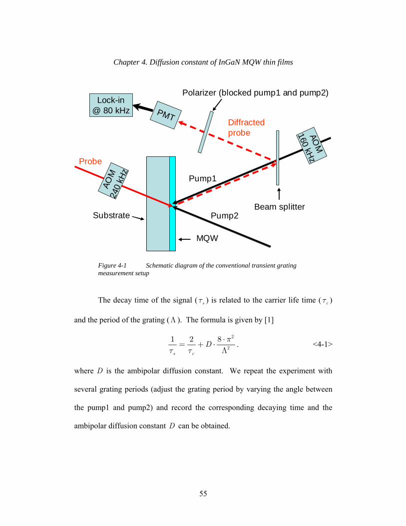
Chapter 4. Diffusion constant of InGaN MQW thin films
MQW
Substrate
Probe
Pump1
Pump2
Diffracted probe
Beam splitter
Polarizer (blocked pump1 and pump2)
PMT
Lock-in@ 80 kHz
AOM
160 kHzAO
M24
0 kH
z
Figure 4-1 Schematic diagram of the conventional transient grating measurement setup
The decay time of the signal ( ) is related to the carrier life time ( )
and the period of the grating (Λ ). The formula is given by [1]
sτ cτ
2
2
1 2 8
s c
Dπ
τ τ⋅
= + ⋅Λ
. <4-1>
where D is the ambipolar diffusion constant. We repeat the experiment with
several grating periods (adjust the grating period by varying the angle between
the pump1 and pump2) and record the corresponding decaying time and the
ambipolar diffusion constant D can be obtained.
55

Chapter 4. Diffusion constant of InGaN MQW thin films
56
In practice, the diffracted probe beam is very weak and can be very
difficult to measure directly. One particularly serious problem is due to the
unwanted interference between the diffracted probe beam and the scattered
probe beam in the direction of the diffracted probe beam. The strength of this
scattered probe may actually be stronger than the diffracted probe, so the
interference signal actually dominates over the diffracted probe signal. One may
think that we can then just measured the interference term and we can still get
the decaying time of the grating. Unfortunately this is very difficult, because the
phase difference between the diffracted probe and the scattered probe is related
to the phase difference between pump1 and pump2. The path length difference
between pump1 and pump2 will be randomly varying on the order of
wavelength due the mechanical vibration of the experiment setup. This effect is
shown in Figure 4-2, the inset is a zoom in view of 0.3 second and it shows that
the signal can undergo a very large change in a very short time span. As a result,
without the path length stabilization control, the interference signal behaves like
noise and obscures the measurement of the power of the diffracted probe beam.
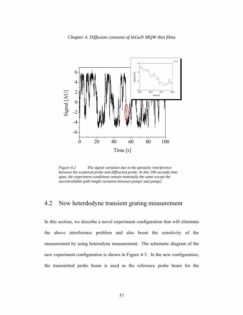
Chapter 4. Diffusion constant of InGaN MQW thin films
0 20 40 60 80 100
-6
-4
-2
0
2
4
6
54.5 54.6 54.7 54.8-5
-4
-3
-2
Sign
al [A
U]
Time [s]
B
Sign
al [A
U]
Time [s]
Figure 4-2 The signal variation due to the parasitic interference between the scattered probe and diffracted probe. In this 100 seconds time span, the experiment conditions remain nominally the same except the uncontrollable path length variation between pump1 and pump2.
4.2 New heterdodyne transient grating measurement
In this section, we describe a novel experiment configuration that will eliminate
the above interference problem and also boost the sensitivity of the
measurement by using heterodyne measurement. The schematic diagram of the
new experiment configuration is shown in Figure 4-3. In the new configuration,
the transmitted probe beam is used as the reference probe beam for the
57

Chapter 4. Diffusion constant of InGaN MQW thin films
heterodyne measurement. The same beam splitter that was used to split the
pump beam into pump1 and pump2 is also used to combine the diffracted probe
beam and reference probe beam. In this configuration, the reference probes
beam and the diffracted probe beam going trough the same path as pump1 and
pump2 respectively. The detail phase analysis given as following will show that
the resulting interference signal between diffracted probe beam and the
reference probe beam is independent of the path length difference between
pump1 and pump2. So the heterodyne measurement can be used without the
stabilization of the path length difference.
58
)
)
) )
r
For the purpose of phase analysis, we assume that the polarization of the
pump is TE (s) polarization and the probe is TM (p) polarization. We define the
transmission coefficient and reflection coefficient for TM (TE) polarization light
incidence from the front side of the beam splitter as and
respectively and the transmission coefficient and reflection
coefficient for TM (TE) polarization light incidence from the back side of the
beam splitter as and respectively. The phase of the
reference probe (transmitted probe) at the detector is given by
, ,(bs TM bs TEt t
, ,(bs TM bs TEr r
, ,(bs TM bs TEt t′ ′, ,(bs TM bs TEr r′ ′
<4-2> ( )1, , 1,
iref TM bs TM TM
i
E r ′= φ + +∑

Chapter 4. Diffusion constant of InGaN MQW thin films
Where is the phase of the optical path length of arm number 1 for TM
polarization light, is the phase of reflection coefficient of the TM light
from the back side of the beam splitter, is the phase of the reflection
coefficient of the i-th mirror for TM light in the path number 1.
1,TMφ
,bs TMr ′
( )1,iTMr
pumpprobe
detection
pump1
pump2
sample
Mirror
diffracted probe
reference probe
Mirror
TE (s)TM (p)
,bs Pr ′
,bs Pt ′,bs Pr
,bs PtBeam splitter
pumpprobe
detection
pump1
pump2
sample
Mirror
diffracted probe
reference probe
Mirror
TE (s)TM (p)
,bs Pr ′
,bs Pt ′,bs Pr
,bs Pt,bs Pr ′
,bs Pt ′,bs Pr
,bs PtBeam splitter
Figure 4-3 Schematic diagram of new heterodyne transient grating measurement setup.
The phase of the diffracted probe is given by
( )2, , 2,
jdif TM bs TM TM grating
j
E t r= φ + + +φ∑ <4-3>
Where is the phase of the optical path length of arm number 2 for TM
polarization light, is the phase of transmission coefficient of the TM
2,TMφ
,bs TMt
59

Chapter 4. Diffusion constant of InGaN MQW thin films
light from the front side of the beam splitter, is the phase of the reflection
coefficient of the i-th mirror for TM light in the path number 2. is the
phase difference between the diffracted and transmitted light of the grating and
is given by
( )2,iTMr
gratingφ
0, 1 2grating grating pump pumpE Eφ = φ + − <4-4>
Where is the phase of the pump 1(2) at the sample. is a
constant that relate to the shape of the grating.
1(2)pumpE 0,gratingφ
The phase of pump1 and pump2 at the sample is given by
( )1 1, , 1,
( )2 2, , 2,
ipump TE bs TE TE
i
jpump TE bs TE TE
j
E t
E r
= + +
= + +
∑
∑
φ
φ
r
r
)
)
<4-5>
Where is the phase of the optical path length of arm number 1 (2)
for TE polarization light. is the phase of the transmission
(reflection) coefficient of the beam splitter for TE light from the front side.
( ) is the phase of the reflection coefficient of the i-th mirror in the
path number 1 (2) for TE light.
1, 2,(TE TEφ φ
, ,(bs TE bs TEt r
( )1,iTEr
( )2,iTEr
From <4-2>, <4-3>, <4-4> and <4-5>, the phase difference between the
diffracted probe and the reference probe is given by
<4-6> 2, 2, 1, 1, 0( ) ( )
dif ref
TM TE TM TE
E Eθ = −
= φ −φ − φ −φ + θ
60

Chapter 4. Diffusion constant of InGaN MQW thin films
Where is a constant that is not related the optical path length of arm 1 and
arm 2 and is given by
0θ
0 0, , , , ,
( ) ( ) ( ) ( )2, 1, 1, 2,
grating bs TM bs TM bs TE bs TE
j i iTM TM TE TE
j
j i i j
t r t r
r r r
′θ = φ + − + −
+ − + −∑ ∑ ∑ ∑ r
Γ
<4-7>
Since the air is an isotropic medium and plug this
into <4-6>
1, 1, 2, 2,,TM TE TM TEφ = φ φ = φ
<4-8> 0θ = θ
This complete the proof that the phase difference between the diffracted probe
and the reference probe is independence of the optical path length of the arm 1
and arm 2.
Under a very special experiment condition, it is possible that and
when this happen, the interference signals between the transmitted probe and
diffracted probe (proportional to cos( ) is exactly zeros and the heterodyne
measurement will fail. To account for this situation, a variable compensator can
be inserted into arm 2 and align the optical axis of the compensator with the
polarization of the light. When the compensator is inserted,
/2θ = π
)θ
<4-9> 1, 1,
2, 2,
0TM TE
TM TE
φ −φ =
φ −φ =
And the phase difference θ is given by
<4-10> 0θ = θ + Γ
61

Chapter 4. Diffusion constant of InGaN MQW thin films
The retardance ( ) of the compensator can be adjusted to maximum the
interference signal.
Γ
Although the measurement using this configuration increases the
detection sensitivity of the diffracted probe beam by using the heterodyne
technique, the signal of measurement is not background free. On top of the
signal due to the transient grating diffracted probe beam (TG), there is also
another signal due the pump induced differential transmission change of the
reference probe beam (DT). These two signals can be separated by doing one
more measurement with the same exact experiment conditions except with a
small mismatch of the path length difference between pump1 and pump2 so that
they are not overlap in time and thus not interfere with each other to form the
grating. In this mismatch case, the TG signal will cease to exist and only DT
signal is left in the measurement. By subtracted the results of this two
measurements, the TG signal can be separated out.
The decay time of the TG signal ( ) is related to the carrier life time
( ) and the period of the grating ( ). The formula is given by
TGτ
cτ Λ
2
2
1 1 4
TG c
Dπ
τ τ⋅
= + ⋅Λ
<4-11>
Where D is the ambipolar diffusion constant. As oppose to the conventional
method, there is no need to change the grating period for one to obtain the
62

Chapter 4. Diffusion constant of InGaN MQW thin films
diffusion constant, because the carrier life time ( ) can be obtained from the
DT signal.
cτ
To further increase the sensitivity of the measurement, lock-in detection
is used and the pump beam is modulated with an acousto-optic modulator at 1.6
MHz (this frequency is choose to avoid the low frequency noise in the
Ti:Sapphire laser). To prevent the scattered pump beam from reaching the
detector, the polarization of the pump beam and the probe beam are
perpendicular to each other and a polarizer is place in front of the detector to
block the pump beam.
4.3 Important optical alignment issue
When doing the experiment setup of the heterodyne transient grating
measurement, it is very important that the total number of mirror in the arm 1
and arm 2 to be differed by an odd number. The alignment will become difficult
if the above rule is not follow. For the purpose to demonstrate that why this is
the case we consider a special case where there is a single mirror in the arm 1
and arm 2 as show in Figure 4-4. The solid line represents the perfect alignment
in which the probe and pump are overlap with each other. The dash line
represents the case where there is a small angle misalignment of δ in the
direction of the probe and pump 1. As can be seen from the figure, the
63

Chapter 4. Diffusion constant of InGaN MQW thin films
diffracted probe and transmitted probe will displace toward different direction
and causing the angle deviation ( ) between the transmitted probe and the
diffracted probe to be increase from 0 to 2 . The angle deviation ϕ has to be
keep below a certain value in order for the detector to be able to measure the
heterodyne signal. The condition is given by
ϕ
δ
40 4 10 radDETr
−λϕ < = × <4-12>
Where (405 nm) is wavelength of the light and (1 mm) is the radius of
the detector.
0λ DETr
pumpprobe
detectionpump1
pump2
sample
Mirror
Mirror
Beam splitterδ
δ
2ϕ = δ
pumpprobe
detectionpump1
pump2
sample
Mirror
Mirror
Beam splitterδ
δ
2δϕ =
Figure 4-4 Experiment configuration with same number of mirrors in both arm.
64
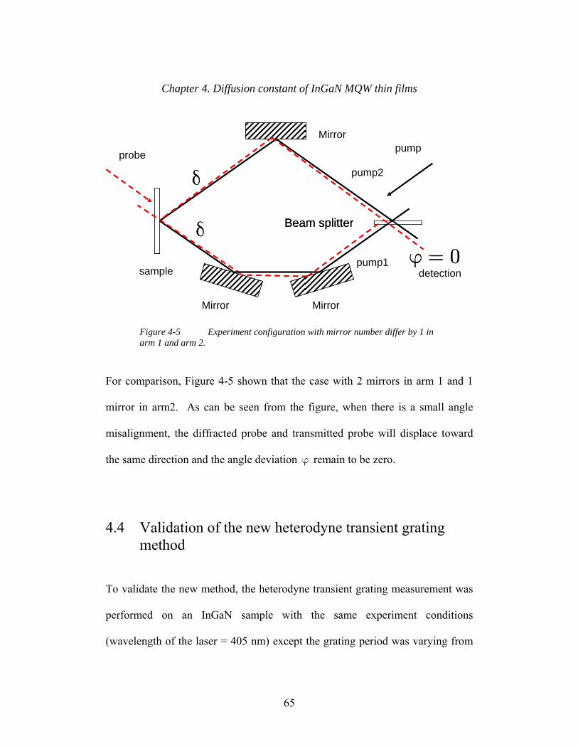
Chapter 4. Diffusion constant of InGaN MQW thin films
pumpprobe
detectionpump1
pump2
sample
Mirror
Mirror
Beam splitterδ
δ
0ϕ =
Mirror
pumpprobe
detectionpump1
pump2
sample
Mirror
Mirror
Beam splitterδ
δ
0ϕ =
Mirror
Figure 4-5 Experiment configuration with mirror number differ by 1 in arm 1 and arm 2.
For comparison, Figure 4-5 shown that the case with 2 mirrors in arm 1 and 1
mirror in arm2. As can be seen from the figure, when there is a small angle
misalignment, the diffracted probe and transmitted probe will displace toward
the same direction and the angle deviation ϕ remain to be zero.
4.4 Validation of the new heterodyne transient grating method
To validate the new method, the heterodyne transient grating measurement was
performed on an InGaN sample with the same experiment conditions
(wavelength of the laser = 405 nm) except the grating period was varying from
65
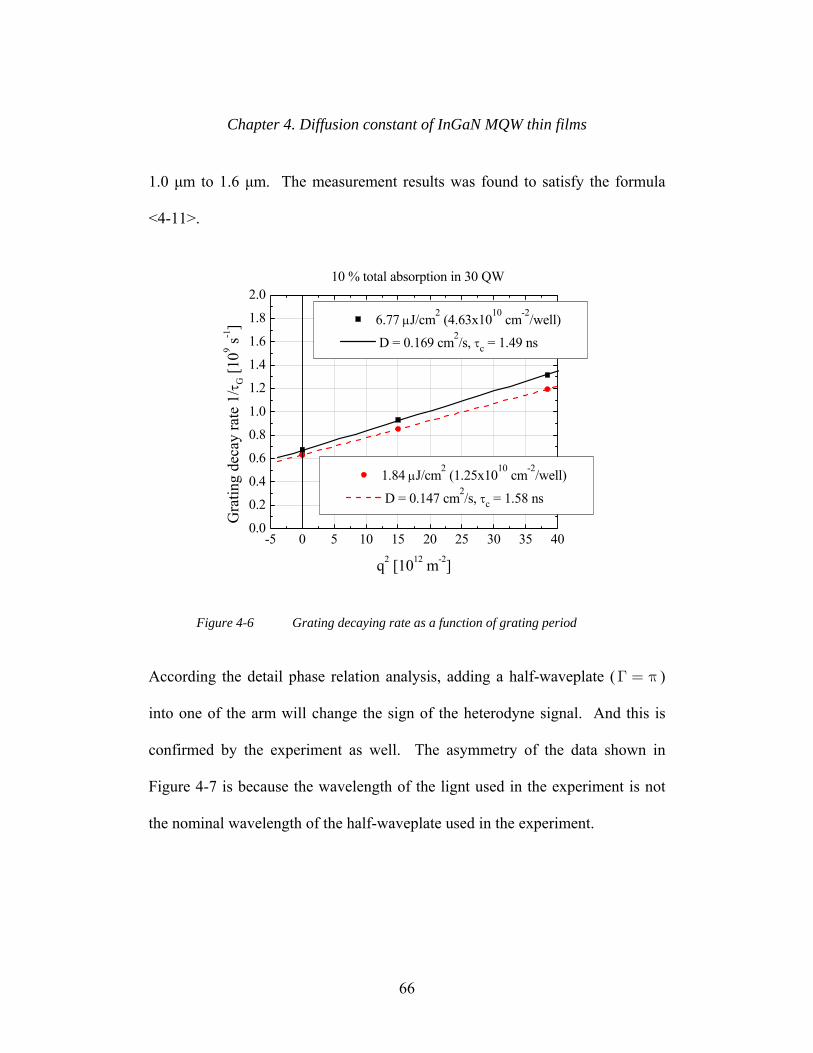
Chapter 4. Diffusion constant of InGaN MQW thin films
1.0 µm to 1.6 µm. The measurement results was found to satisfy the formula
<4-11>.
-5 0 5 10 15 20 25 30 35 400.0
0.2
0.4
0.6
0.8
1.0
1.2
1.4
1.6
1.8
2.0
1.84 µJ/cm2 (1.25x1010 cm-2/well)
D = 0.147 cm2/s, τc = 1.58 ns
6.77 µJ/cm2 (4.63x1010 cm-2/well)
D = 0.169 cm2/s, τc = 1.49 ns
Gra
ting
deca
y ra
te 1
/τG [1
09 s-1]
q2 [1012 m-2]
10 % total absorption in 30 QW
Figure 4-6 Grating decaying rate as a function of grating period
According the detail phase relation analysis, adding a half-waveplate ( )
into one of the arm will change the sign of the heterodyne signal. And this is
confirmed by the experiment as well. The asymmetry of the data shown in
Figure 4-7 is because the wavelength of the lignt used in the experiment is not
the nominal wavelength of the half-waveplate used in the experiment.
Γ = π
66

Chapter 4. Diffusion constant of InGaN MQW thin films
-200 0 200 400 600 800 1000 1200 1400
0.0
0.2
0.4
0.6
0.8
1.0 P1&P2 overlap not overlap overlap with HWP
∆P/P
[10-4
]
Delay [ps]
(a)
(b)
(c)
Figure 4-7 Heterodyne signal (a) pump1 and pump2 overlap and no half-waveplate (HWP), (b) pump1 and pump2 overlap and with HWP in one arm, (c) pump1 and pump2 not overlap
4.5 Diffusion constant of InGaN MQW
The measurement results in this session is measured on a multiple-quantum-well
(MQW) InGaN thin film sample with 30 period of 2.5 nm well, 8 nm n-doped
barrier (The schematic of the sample structure is shown in Figure 4-8). The
photoluminescence (PL) of the sample is shown in Figure 4-9. From the PL
spectrum, it is clear that the sample is not uniform across the sample. We will
use this fact to study the dependence of the diffusion constant on the
composition of InGaN. Unless otherwise states, all the results present in this
67

Chapter 4. Diffusion constant of InGaN MQW thin films
chapter are measured with 405 nm excitation. From the peak of the PL
spectrum in Figure 4-9, assuming that the non-uniform of the sample is all due
to the composition variation, the composition is found to be vary between
In0.1Ga0.9N and In0.15Ga0.85N. If we assume the fixed composition In0.13Ga0.87N,
the well width is vary between 1.5 nm and 4 nm.
(0001) Al2O3 Substrate
GaN buffer layer
In0.12Ga0.88N (2.5 nm)
In0.02Ga0.98N (8.0 nm n-doped)30 period
(0001) Al2O3 Substrate
GaN buffer layer
In0.12Ga0.88N (2.5 nm)
In0.02Ga0.98N (8.0 nm n-doped)30 period
Figure 4-8 Sample structure of InGaN MQW thin film
68

Chapter 4. Diffusion constant of InGaN MQW thin films
375 400 425 4500
5
10
15
20Position
-1mm 1mm 3mm 5mm
PL [A
.U.]
Wavelength [nm]
405nm
Figure 4-9 The photoluminescence spectrum at various position on the InGaN MQW sample.
In order to choose which spot on the sample to do the measurement, we do a
series of differential transmission measurements a various position. The
differential transmission signal ( ) at long delay at various position is
plot in Figure 4-10.
/T T∆
69

Chapter 4. Diffusion constant of InGaN MQW thin films
-4 -3 -2 -1 0 1 2 3 4 5 60.0
0.5
1.0
1.5
2.0
2.5
3.0
∆T/T
[10-4
]
Position [mm]
Figure 4-10 Differential transmission signal at long delay across the sample (405 nm excitation wavelength)
The diffusion constant at various position on the sample is shown in Figure 4-11.
As can be seen from the figure, the diffusion constant is fairly constant across
the sample ~ 0.18 cm2/s. Using the Einstein relationship, the ambipolar mobility
can be found to be 7.2 cm2/Vs and the hole mobility is 3.6 cm2/Vs. This number
is consistence with the numbers of hole mobility of that have been report in the
literature [2].
70

Chapter 4. Diffusion constant of InGaN MQW thin films
0.00
0.04
0.08
0.12
0.16
0.20
-4 -3 -2 -1 0 1 2 3 4 5 60.00
0.04
0.08
0.12
0.16
0.20
Diffusion constant
Diff
usio
n C
onst
ant [
cm2 /s
]
Position [mm]
Diffusion length
Diff
usio
n Le
ngth
[µm
]
Figure 4-11 Diffusion constant and diffusion length across the sample (405nm excitation wavelength).
Figure 4-12 shown that the diffusion constant increase as the temperature
increase. Figure 4-13 shown that the diffusion constant increase as the photo-
generated carrier density increase. Both this behavior suggests that the localized
state play an important role in the carrier transport. At elevated temperature, the
localized carrier can be thermally excited out of the localized state and thus the
increase of the diffusion constant. As the number of photo-generated carrier
density increase, most of the localized state will be filled up and more carriers
will occupied the de-localized state and lead to an increase in the diffusion
constant.
71

Chapter 4. Diffusion constant of InGaN MQW thin films
50 100 150 200 250 300 350 400 450 500
0.0
0.1
0.2
0.3
0.4
0.5
0.6
0.7
(a)
(d)(b)
Position -1mm 1mm 3mm 5mm
GaN:Mg 1 GaN:Mg 2 InGaN: Mg
Am
bipo
lar d
iffus
ion
cons
tant
[cm
2 /s]
Temperature [K]
(c)
Figure 4-12 The temperature dependent of the diffusion constant. (a) 30 QW 2.5nm In0.13Ga0.87N is my measurement data, (b) and (c) are calculated from the measured mobility data of p-GaN taken from[3] using Einstein relation, (d) are calculated from the measured mobility data of p-In0.09Ga0.91N taken from [2] using Einstein relation.
1016 1017 1018 1019 1020
0.01
0.1
1
10
(a) (b) (c) Calculated
Diff
usio
n co
nsta
nt [c
m2 /s
]
Photo Generated Carrier Density [1/cm3]
72

Chapter 4. Diffusion constant of InGaN MQW thin films
Figure 4-13 The power dependent of the diffusion constant, (a) 30 QW 2.5nm In0.13Ga0.87N is my measurement data, (b) 6 QW 3.4nm In0.3Ga0.7N and (c) 10 QW 4nm In0.3Ga0.7N are taken from [4].
4.6 Diffusion model
It is important to recognize that the diffusion constant that measure with the
transient grating method is the ambipolar diffusion constant. The ambipolar
diffusion constant is given by (page 87 in [5])
p n n pa
n p
D n D pD
n p
µ + µ=
µ + µ <4-13>
Where is the electron (hole) diffusion constant, is the electron
(hole) mobility, is the electron (hole) carrier density.
(n pD D ) ( )n pµ µ
( )n p
Here we introduce a simple model shown in Figure 4-14 we consider only the
heave-hole subband in the valence band and also we assume that there is a
localized state with energy level and the density of the localized state is
given by . We assume that the relaxation between the localized state and the
extended state is fast that they share a common quasi Fermi level ( ).
loc,pE
locP
FpE
73

Chapter 4. Diffusion constant of InGaN MQW thin films
locP
FpE E=
loc,pE E=
0hhE E= =h2
( )m
EL
ρ =π
locP
FpE E=
loc,pE E=
0hhE E= =h2
( )m
EL
ρ =π
Figure 4-14 Schematic of the diffusion model
The hole occupy in the extended state is given by
Fph Bext 2
B
ln[1 exp( )]Em k T
pL k
−= +
π T <4-14>
Where T is the temperature, is the Plank’s constant, is the Boltzmann’s
constant, L is the width of the quantum well, is the effective mass of the
hole.
Bk
hm
The hole occupy in the localized state is given by
locloc
Fp loc,p
B
1 exp( )
Pp E E
k T
= −+
<4-15>
The total number of hole is given by
<4-16> ext locp p p= +
Using the Boltzmann transport equation and under the relaxation time
approximation, the mobility and diffusion constant of hole is given by [6]
74

Chapter 4. Diffusion constant of InGaN MQW thin films
ext
Fpext
p
ph
pFpp p
h
qt pm p
dE dEp tD p
q dp dp m
µ =
= − µ = − <4-17>
Where is the electron charge, is the hole effective mass, q hm pt is the
relaxation time of hole.
A similarly model can be applied to the conduction band. The hole occupy in
the extended state is given by
c B Fnext 2
B
ln[1 exp( )]m k T E
nL k
= +π T
<4-18>
Where is the electron effective mass, is the electron quasi Fermi level. cm FnE
The electron occupy in the localized state is given by
locloc
loc,n Fn
B
1 exp( )
Nn E E
k T
= −+
<4-19>
Where is the localized energy level near the conduction band, is the
density of the localized state near the conduction band.
loc,nE locN
The total number of electron is given by
<4-20> ext locn n n= +
The mobility and diffusion constant of hole is given by
75

Chapter 4. Diffusion constant of InGaN MQW thin films
ext
Fn Fnext
n
nc
n
n nc
qt nm n
n dE dE tD n
q dp dn m
µ =
= µ = <4-21>
Where is the electron charge, is the electron effective mass, q cm nt is the
relaxation time of electron.
Under the optical excitation, same number of electron and hole is generated
<4-22> back
back
n N s
p P s s
= +
= + ≈
Where is the background electron (hole) carrier density, s is the
photo-generated carrier density. The background electron carrier density
is not negligible because the barrier is n-doped.
(back backN P )
backN
For an optical excitation level (s ), the quasi Fermi level of electron and hole can
be found by solving <4-16> and <4-20> combine with <4-22>. From there the
mobility and diffusion constant of electron and hole can be obtained from
<4-17> and <4-21>. The ambipolar diffusion constant is then calculate with
<4-13>.
In the numerical calculation, the following value have been used
0 0
loc,n loc,p
18 3 18 3loc loc
17 3
0.2 ; 1.2
100 ; 150
10 ; 5.5 10
0.1 ; 10
c h
n p back
m m m m
E meV E meV
N cm P c
t t ps N cm
− −
−
= =
= − =
= =
= = =
m× <4-23>
76

Chapter 4. Diffusion constant of InGaN MQW thin films
77
The calculation results are plot in Figure 4-12 and Figure 4-13. The calculation
results agree with the measurement data reasonably well. The proposed model
is able to reproduce the qualitative behaviors of the diffusion constant increase
as the temperature increase and the diffusion constant increase as the photo-
generated carrier density increase.
4.7 Summary and future work
In summary, a novel heterodyne transient grating measurement without the need
of electronic feedback stabilization has been developed and used to measure the
diffusion constant of InGaN MQW thin film. The measure diffusion constant is
very small (~0.2 cm2/s), indicated that the carrier localization play an important
role in the carrier transport. A simple model has been developed to explain the
temperature dependence and the carrier density dependence of the diffusion
constant.
The heterodyne transient grating developed in this chapter is a very
powerful method to study the carrier transport in thin film sample. Due to the
system limitation, only temperature around the room temperature is accessible to
our experiment. Measurement at lower and higher temperature should give us
more information about the carrier transport properties. Performing the

Chapter 4. Diffusion constant of InGaN MQW thin films
78
measurement with higher photo-generated carrier density will also shed more
light on the carrier transport behavior.
4.8 Reference [1] H. J. Eichler, P. Gunter, and S. W. Pohl, Laser-Induced Dynamics
Gratings. Berlin: Springer-Verlag, 1986. [2] S. Yamasaki, S. Asami, N. Shibata, M. Koike, K. Manabe, T. Tanaka, H.
Amano, and I. Akasaki, "p-type conduction in Mg-doped Ga0.91In0.09N grown by metalorganic vapor-phase epitaxy," Applied Physics Letters, vol. 66, pp. 1112-1113, 1995.
[3] T. Tanaka, A. Watanabe, H. Amano, Y. Kobayashi, I. Akasaki, S. Yamazaki, and M. Koike, "p-type conduction in Mg-doped GaN and Al0.08Ga0.92N grown by metalorganic vapor phase epitaxy," Applied Physics Letters, vol. 65, pp. 593-594, 1994.
[4] A. Vertikov, I. Ozden, and A. V. Nurmikko, "Diffusion and relaxation of excess carriers in InGaN quantum wells in localized versus extended states," Journal of Applied Physics, vol. 86, pp. 4697-4699, 1999.
[5] S. M. Sze, Physics of Semiconductor Devices, 2-nd ed. New York: John Wiley & Sons, 1981.
[6] J. R. Christman, Fundamentals of Solid State Physics. New York: John Wiley & Sons, 1988.

Chapter 5. Summary and future work
Chapter 5. Summary and future work
5.1 Gain measurement
In Chapter 2, we have used the FT method to measure and calculate the gain
spectrum, linewidth enhancement factor (3 ~ 15), ground index (3.2 ~ 3.55),
group velocity dispersion (-20 µm-1 ~ -40 µm-1), differential gain (
cm
170.2 10−×
2 ~ cm171 10−× 2), carrier-induced index change ( cm220.5 10−− × 3 ~
cm221 10−− × 3) and thermal-induce index change ( K41.3 10−× -1) for an
InGaN MQW laser diode in the wavelength range between 400 nm and 410 nm.
5.2 Valence intersubband relaxation
In Chapter 3, the femtosecond carrier dynamics in InGaN MQW laser diode
were studied using time-resolved bias-lead monitoring technique at low carrier
density region and the dynamics at high carrier density region were studied
using time-resolved differential reflection measurement. In both regions, the
carrier dynamics were found to be consistent with the presence of an ultrafast
79

Chapter 5. Summary and future work
inter-subband hole relaxation process between the TM-sensitive subbands (LH2,
HH2) and TE-sensitive subbands (LH1, HH1). The time constant of the transfer
process is within the time resolution of the experiment instrument (τ < 0.37 ps).
The differential transmission measurement is a preferred method to study
the carrier dynamics. In this thesis, due to the limitation of the sample,
differential transmission measurement is not possible. In the future, if the back
facet of the laser diode is accessible, measurement described in [1-3] should be
performed to make a more detailed analysis of the valence intersubband
relaxation dynamics.
Measurement on the a-plane (or m-plane) InGaN thin film sample can
also shed more light on the valence intersubband relaxation because a-plane
corresponds to the mirror facet of the InGaN laser diode. Measurement on the
a-plane sample had been tried, but repeatable measurement can not be obtained
due to the surface roughness and uniformity of the sample. In the future, when
the better quality a-plane (m-plane) sample is available, the measurement should
be performed to gain more insight to the valence intersubband relaxation
dynamics.
5.3 Carrier transport in InGaN
80

Chapter 5. Summary and future work
The heterodyne transient grating developed in chapter 4 is a very powerful
method to study the carrier transport in thin film sample. This novel heterodyne
transient grating measurement eliminated need of electronic feedback
stabilization. We have used this method to measure the diffusion constant of
InGaN MQW thin film. The measure diffusion constant is very small (~0.2
cm2/s), indicated that the carrier localization play an important role in the carrier
transport. A simple model has been developed to explain the temperature
dependence and the carrier density dependence of the diffusion constant.
Due to the system limitation, only temperature around the room
temperature is accessible to our experiment. Measurement at lower and higher
temperature should give us more information about physical mechanism that
governs the carrier transport properties. Performing the measurement with
higher photo-generated carrier density will also shed more light on the carrier
transport behavior.
5.4 Reference [1] K. L. Hall, A. M. Darwish, E. P. Ippen, U. Koren, and G. Raybon,
"Femtosecond index nonlinearities in InGaAsP optical amplifiers," Applied Physics Letters, vol. 62, pp. 1320-1322, 1993.
[2] C. T. Hultgren and E. P. Ippen, "Ultrafast refractive index dynamics in AlGaAs diode laser amplifiers," Applied Physics Letters, vol. 59, pp. 635-637, 1991.
81

Chapter 5. Summary and future work
[3] C. K. Sun, H. K. Choi, C. A. Wang, and J. G. Fujimoto, "Femtosecond gain dynamics in InGaAs/AlGaAs strained-layer single-quantum-well diode lasers," Applied Physics Letters, vol. 63, pp. 96-98, 1993.
82


![[PPT]Gallium Nitride (GaN) - Ohio - Physics & Astronomyhla/GaN-1.ppt · Web viewGallium Nitride (GaN) PHYS 571 ... ZnO, CdS, CdSe, and other semiconductors. ... Company: Hewlett-Packard](https://static.fdocuments.in/doc/165x107/5abecaa87f8b9aa15e8d48a6/pptgallium-nitride-gan-ohio-physics-hlagan-1pptweb-viewgallium-nitride.jpg)