Characteristics of InGaN-Based Light-Emitting Diodes on Patterned

Capability of GaN based micro-light emitting
diodes operated at the injection level of kA/cm2 Q.Q.Jiao1, Z.Z.Chen1*, J.Ma1, S.Y.Wang1, Y.Li1, S.Jiang1, Y.L.Feng1, J.Z.Li1,
Y.F.Chen1, T.J.Yu1, S.F.Wang1, G.Y.Zhang1,3, P.F.Tian2, E.Y.Xie2, Z.Gong2, E.D.Gu2,
M.D.Dawson2 1State Key Laboratory for Artificial Microstructure and Mesoscopic Physics, School of Physics, Peking University,
Beijing 100871, China 2Institute of Photonics, University of Strathclyde, Glasgow G4 0NW, Scotland, United Kingdom
3Sino Nitride Semiconductor Co., Ltd, Dongguan 523500, Guangdong, China
Abstract: Electrical and optical properties of different size InGaN/GaN
micro-LEDs (μLEDs) are investigated in high injection level.
Electroluminescence (EL) results show that 10 μm diameter LED can be
well operated under current density above 16 kA/cm2, while the 300 μm
one can only endure 226 A/cm2. Streak camera time resolved
photoluminescence (TRPL) results show obviously that the decay rate is
much faster for smaller size μLED because of less band-gap
renormalization (BGR). Combining with APSYS simulation, the high
injection level carriers transportation and recombination mechanisms are
investigated in terms of current spreading, BGR and strain relaxation.
2014 Optical Society of America
OCIS codes: (230.3670) Light-emitting diodes; (250.0250) Optoelectronics.
References and links
1. Y. C. Shen, G. O. Mueller, S. Watanabe, N. F. Gardner, A. Munkholm, and M. R. Krames, “Auger
recombination in InGaN measured by photoluminescence,” Appl. Phys. Lett. 91(14), 141101 (2007).
2. David S. Meyaard, Qifeng Shan, Jaehee Cho, E. Fred Schubert, Sang-Heon Han, Min-Ho Kim, Cheolsoo Sone,
Seung Jae Oh, and Jong Kyu Kim, “Temperature dependent efficiency droop in GaInN light-emitting diodes
with different current densities,” Appl. Phys. Lett. 100(8), 081106 (2012).
3. Giovanni Verzellesi, Davide Saguatti, Matteo Meneghini, Francesco Bertazzi, Michele Goano, Gaudenzio
Meneghesso, and Enrico Zanoni , “Efficiency droop in InGaN/GaN blue light-emitting diodes: Physical mechanisms and remedies,” J. Appl. Phys. 114(7), 071101 (2013).
4. N. F. Gardner, G. O. Müller, Y. C. Shen, G. Chen, S. Watanabe, W. Götz, and M. R. Krames, “Blue emitting
InGaN/GaN double-heterostructure light-emitting diodes reaching maximum quantum efficiency above 200
A/cm2,” Appl. Phys. Lett. 91(24), 243506 (2007).
5. Min-Ho Kim, Martin F. Schubert, Qi Dai, Jong Kyu Kim, E. Fred Schubert, Joachim Piprek, and Yongjo Park, “Origin of efficiency droop in GaN-based light-emitting diodes,” Appl. Phys. Lett. 91(18), 183507 (2007).
6. Chun-Ta Yu, Wei-Chih Lai, Cheng-Hsiung Yen, and Shoou-Jinn Chang, “Effects of InGaN layer thickness of
AlGaN/InGaN superlattice electron blocking layer on the overall efficiency and efficiency droops of
GaN-based light emitting diodes,” Optics express, 22( S3), A663- A670 ( 2014).
7. Kwang-Choong Kim, Mathew C. Schmidt, Hitoshi Sato, Feng Wu, Natalie Fellows, Zhongyuan Jia, Makoto
Saito, Shuji Nakamura, Steven P. DenBaars, James S. Speck, and Kenji Fujito, “Study of nonpolar m -plane InGaN/GaN multiquantum well light emitting diodes grown by homoepitaxial metal-organic chemical vapor
deposition,” Appl. Phys. Lett. 91(18), 181120 (2007).
8. Michael J. Cich, Rafael I. Aldaz, Arpan Chakraborty, Aurelien David, Michael J. Grundmann, Anurag Tyagi,
Meng Zhang, Frank M. Steranka, and Michael R. Krames, “Bulk GaN based violet light-emitting diodes with high efficiency at very high current density,” Appl. Phys. Lett. 101(22), 223509 (2012).
9. C. H. Wang, S. P. Chang, P. H. Ku, J. C. Li, Y. P. Lan, C. C. Lin, H. C. Yang, H. C. Kuo, T. C. Lu, S. C. Wang,
and C. Y. Chang, “Hole transport improvement in InGaN/GaN light-emitting diodes by graded-composition
multiple quantum barriers, Appl. Phys. Lett. 99(17), 171106 (2011).
10. H. P. T. Nguyen, S. Zhang, K. Cui, X. Han, S. Fathololoumi, M. Couillard, G. A. Botton, and Z. Mi, “p-Type Modulation Doped InGaN/GaN Dot-in-a-Wire White-Light-Emitting Diodes Monolithically Grown on Si(111),”
* e-mail: [email protected]

Nano. Lett. 11(5), 1919-1924(2011).
11. A. Castiglia, D. Simeonov, H. J. Buehlmann, J.-F. Carlin, E. Feltin, J. Dorsaz, R. Butté, and N. Grandjean,
“Efficient current injection scheme for nitride vertical cavity surface emitting lasers,” Appl. Phys. Lett. 90(3), 033514 (2007).
12. Michael C. Y. Huang, Ye Zhou, and Connie J. Chang-Hasnain, “Single mode high-contrast subwavelength
grating vertical cavity surface emitting lasers,” Appl. Phys. Lett. 92(17), 171108 (2008).
13. Zheng Gong, Shirong Jin, Yujie Chen, Jonathan McKendry, David Massoubre, Ian. M. Watson, Erdan Gu, and
Martin D. Dawson, “Size-dependent light output, spectral shift, and self-heating of 400 nm InGaN light emitting Diodes,” J. Appl. Phys. 107(1), 013103 (2010).
14. Y. B. Tao, S. Y. Wang, Z. Z. Chen, Z. Gong, E. Y. Xie, Y. J. Chen, Y. F. Zhang, J. McKendry, D. Massoubre,
E. D. Gu, B. R. Rae, R. K. Henderson and G. Y. Zhang, “Size effect on efficiency droop of blue light emitting
diode,” Phys. Status Solidi C, 9(3-4), 616-619 (2012).
15. Pengfei Tian, Jonathan J. D. McKendry, Zheng Gong, Benoit Guilhabert, Ian M. Watson, Erdan Gu,Zhizhong Chen,Guoyi Zhang, and Martin D. Dawson, “Size-dependent efficiency and efficiency droop of blue InGaN
micro-light emitting diodes,” Appl. Phys. Lett. 101(23), 231110 (2012).
16. Tae-il Kim , Yei Hwan Jung , Jizhou Song , Daegon Kim , Yuhang Li , Hoon-sik Kim ,Il-Sun Song , Jonathan J.
Wierer , Hsuan An Pao , Yonggang Huang , and John A. Rogers, “High-Efficiency, Microscale GaN Light-Emitting Diodes and Their Thermal Properties on Unusual Substrates,” small 8(11), 1643–1649(2012).
17. N. Lobo Ploch, H. Rodriguez, C. Stölmacker, M. Hoppe, M. Lapeyrade, J. Stellmach, F. Mehnke, Tim
Wernicke, A. Knauer, V. Kueller, M. Weyers, S. Einfeldt, and M. Kneissl, “Effective Thermal Management in
Ultraviolet Light-Emitting Diodes With Micro-LED Arrays,” IEEE Transactions on Electron Devices, 60(2), 782-786(2013).
18. Han-Youl Ryu and Jong-In Shim, “Effect of current spreading on the efficiency droop of InGaN light-emitting
diodes,” Opt. Express, 19(4), 2886-2894 (2011).
19. David S. Meyaard, Guan-Bo Lin, Jaehee Cho, E. Fred Schubert, Hyunwook Shim, Sang-Heon Han, Min-Ho
Kim, Cheolsoo Sone, and Young Sun Kim, “Identifying the cause of the efficiency droop in GaInN light-emitting diodes by correlating the onset of high injection with the onset of the efficiency droop,” Appl.
Phys. Lett. 102(25), 251114 (2013).
20. Guibao Xu, Guan Sun, Yujie J. Ding, Hongping Zhao, Guangyu Liu, Jing Zhang, and Nelson Tansu, “Investigation of large Stark shifts in InGaN/GaN multiple quantum wells,” J. Appl. Phys. 113(3), 033104
(2013).
21. Martin Feneberg, Sarah Osterburg, Karsten Lange, Christian Lidig, Bernd Garke, and Rüdiger Goldhahn,
Eberhard Richter and Carsten Netzel, Maciej D. Neumann and Norbert Esser, “Band gap renormalization and Burstein-Moss effect in silicon- and germanium-doped wurtzite GaN up to 1020 cm−3,” Phys. Rev. B, 90(7),
075203 (2014).
22. F. Binet, J. Y. Duboz, J. Off and F. Scholz, “High-excitation photoluminescence in GaN: Hot-carrier effects
and the Mott transition,” Phys. Rev. B, 60(7), 4715-4722(1999).
23. Mi-Ra Kim, Cheol-Hoi Kim, Baik-Hyung Han, “Band-gap renormalization and strain effects in semiconductor quantum wells,” Phys. B 245(1), 45-51 (1998).
24. K. Jarašiunas, S. Nargelas, R. Aleksiejunas, S. Miasojedovas, M. Vengris, S. Okur, H. Morkoc¸ U. Ӧzgür, C.
Giesen, Ӧ. Tuna, and M. Heuken, “Spectral distribution of excitation-dependent recombination rate in an
In0.13Ga0.87N epilayer,” J. Appl. Phys. 113(10), 103701 (2013).
25. N. I. Bochkareva, V. V. Voronenkov, R. I. Gorbunov, A. S. Zubrilov, P. E. Latyshev, Yu. S. Lelikov, Yu. T. Rebane, A. I. Tsyuk, and Yu. G. Shreter, “Effect of Localized Tail States in InGaN on the Efficiency Droop in
GaN Light-Emitting Diodes with Increasing Current Density,” Semiconductors, 46( 8), 1032-1039(2012).
26. Shih-Wei Feng, Yung-Chen Cheng, Yi-Yin Chung, C. C. Yang, Yen-Sheng Lin, Chen Hsu, Kung-Jeng Ma,
Jen-Inn Chyi, “Impact of localized states on the recombination dynamics in InGaN/GaN quantum well structures,” J. Appl. Phys. 92(8), 4441(2002).
27. Rattier M., Bensity H., Stanley R. P., et al. “Toward ultra-efficient aluminum oxide microcavity light-emitting
diodes: Guided mode extraction by photonic crystals” IEEE J. Selected Topics in Quant. Electron. 8, 238
(2002)
28. Y. Rosenwaks, M. C. Hanna, D. H. Levi, D. M. Szmyd, R. K. Ahrenkiel, and A. J. Nozik, “Hot-carrier cooling in GaAs: Quantum wells versus bulk,” Phys. Rev. B, 48(19), 14675(1993).
29. V. Ramesh, A. Kikuchi, K. Kishino, M. Funato, and Y. Kawakami, “Strain relaxation effect by nanotexturing
InGaN/GaN multiple quantum well,” J. Appl. Phys. 107(11), 114303 (2010).
30. Qiming Li, Karl R. Westlake, Mary H. Crawford, Stephen R. Lee, Daniel D. Koleske, Jeffery J. Figiel, Karen C.
Cross, Saeed Fathololoumi, Zetian Mi, and George T. Wang, “Optical performance of top-down fabricated InGaN/GaN nanorod light emitting diode arrays,” Opt. Express. 19(25), 25528-25534(2011).

1. Introduction
Although the luminous efficiency have been achieved more than 300 lm/W, the efficiency
droops appear disappointedly in the most excellent light emitting diodes (LEDs) under high
injection level or high temperature [1,2]. By now few conventional LEDs can work for
current densities in the order of hundreds of A/cm2. The origins of the efficiency droop can be
roughly divided into three categories, including internal nonradiative losses, electron leakage
and junction temperature [3]. Many remedies have been reported, such as double
heterostructure (DH) active layer [4], polarization matched barriers and electron blocking
layer [5, 6], nonpolar LED [7], GaN homogeneous epitaxy on freestanding substrate [8],
improved hole injection [9], and so on. Some researchers have been achieved the current
density more than 500 A/cm2 for nanorod LEDs with low efficiency droop [10]. The high
cost nano-processing, point defects and self-heating may hinder these LEDs to practical
application.
Recently, much attention has been paid to the specific small chip size, tens micron LEDs
(μLEDs), which can effectively reduce droop phenomenon, even endure high current density
of several kA/cm2 [11-17]. More uniform current spreading for smaller size LED has been
found by some groups [13, 15, 17]. The efficiency droop will be alleviated for tens micron
LED since the current spreading length is more than 50 μm for the general LED epi-structures
[15, 18]. On the other hand, the junction temperature (Tj) is also decreased when the size of
LED is reduced because of the thermal dissipation and uniform current spreading [2, 13,
16-17]. Generally, current spreading and Tj distribution seem to be the main factors for high
current endurance of μLEDs. Low Tj may improve the luminous efficiency of μLED, but not
well affect the high injection performance [2]. Even if the conventional broad LEDs are
driven by high low-duty pulsed current, they cannot endure one order higher current density.
However, the maximum endured current density is still increased as the size of μLEDs
reducing down below the current spreading length. There are few considerations beyond the
current spreading and Tj.
It is noted that certain amount injected carriers are extracted by the drift field in p-type
electron barrier layer and p-GaN quasi-neutral region [19], the concentration of the trapped
carriers in QWs could reach 1019 cm-3 with the current density above several hundred A/cm2.
Band-gap renormalization (BGR) and band-filling will be happened when the carrier
concentration is more than mid 1018 cm-3 [20-22]. Kim et al found that the BGR effect was
strengthened with an increase of the biaxial compressive strain [23]. What is more important,
the BGR can build an additional potential barrier for carriers to inhibit their transferring from
high-to-low energy state, thus leading to efficiency saturation [24]. Band-filling model
including localized state, extended state and mobility edge has been also used to investigate
the recombination processes under high injection level [21, 25-26]. The above theories may
be useful for understanding the high injection performance of smaller μLEDs.
In this work, the different size μLEDs were fabricated using a compatible process with
the conventional LED. The electroluminescence (EL) spectra were measured on the different
size μLEDs. The remarkable performances under the injection level of kA/cm2 were achieved
for small size μLEDs. Current distributions along the mesa of μLEDs were obtained with the
simulations by the APSYS software package. The carrier dynamic recombination process for
μLEDs was investigated by the time-resolved photoluminescence (TRPL) measurements
under high excitation power.
2. Experiments:
The μLED structure grown by metal organic chemical vapor deposition (MOCVD) was
comprised of a nucleation layer on the sapphire substrate, a 2 μm undoped-GaN layer, a 2.5
μm n-GaN layer, a ten-period InGaN(2.2 nm)/GaN(15 nm) multiple quantum well (MQW)
with the emission wavelength at about 460 nm, and a 230 nm-thick p-GaN layer. The sizes of
active regions were defined from 300 to 10 μm by conventional photolithography and
inductively coupled plasma (ICP) etching. The other detailed fabrication procedures for EL
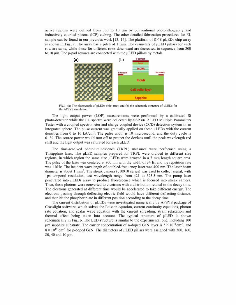
sample can be found in our previous work [13, 14]. The platform of 8×8 μLEDs chip array
is shown in Fig.1a. The array has a pitch of 1 mm. The diameters of μLED pillars for each
row are same, while those for different rows downward are decreased in sequence from 300
to 10 μm. The p-pad squares are connected with the μLED pillars by metals.
Fig.1. (a) The photograph of μLEDs chip array and (b) the schematic structure of μLEDs for
the APSYS simulation.
The light output power (LOP) measurements were performed by a calibrated Si
photo-detector while the EL spectra were collected by SSP 6612 LED Multiple Parameters
Tester with a coupled spectrometer and charge coupled device (CCD) detection system in an
integrated sphere. The pulse current was gradually applied on these μLEDs with the current
densities from 0 to 16 kA/cm2. The pulse width is 10 microsecond, and the duty cycle is
0.1%. The source power would turn off to protect the devices until the peak wavelength red
shift and the light output was saturated for each μLED.
The time-resolved photoluminescence (TRPL) measures were performed using a
Ti:sapphire laser. The μLED samples prepared for TRPL were divided to different size
regions, in which region the same size μLEDs were arrayed in a 5 mm length square area.
The pulse of the laser was centered at 800 nm with the width of 34 fs, and the repetition rate
was 1 kHz. The incident wavelength of doubled-frequency laser was 400 nm. The laser beam
diameter is about 1 mm2. The streak camera (c10910 series) was used to collect signal, with
1ps temporal resolution, test wavelength range from 421 to 525.5 nm. The pump laser
penetrated into μLEDs array to produce fluorescence which is focused into streak camera.
Then, these photons were converted to electrons with a distribution related to the decay time.
The electrons generated at different time would be accelerated to take different energy. The
electrons passing through deflecting electric field would have different deflecting distance,
and then hit the phosphor plate in different position according to the decay time.
The current distribution of μLEDs were investigated numerically by APSYS package of
Crosslight software, which solves the Poisson equation, current continuity equations, photon
rate equation, and scalar wave equation with the current spreading, strain relaxation and
thermal effect being taken into account. The typical structure of μLED is shown
schematically in Fig.1b. The LED structure is similar to the experimental one, including 100
μm sapphire substrate. The carrier concentration of n-doped GaN layer is 5×1018 cm-3, and
8×1017 cm-3 for p-doped GaN. The diameters of μLED pillars were assigned with 300, 160,
80, 40 and 10 μm.

3. Results and analysis
Fig.2. The dependencies of light output power in EL spectra on the current density for 10, 20,
40, 80, 160 and 300 μm LEDs.
Fig.2 shows the dependencies of light output power (LOP) on the current density (L-I)
for μLEDs with different diameters. The L-I curves show that the small size μLEDs can
endure high current density. 10 μm LED is survived at extremely high current density of 16
kA/cm2. The LOP seems not saturate at so high injection level, while that of 300μm LED is
saturated at the current density of 226 A/cm2. The endurable current densities for μLEDs are
higher than ones in our previous work [13] because the most surrounding area with p-type
GaN mesa is covered with n-contact metal. The LOP of 10μm LED is 3.5 times as that of
300μm LED at 200 A/cm2. The efficiency improvement under high injection level for small
size μLED may be attributed to low Tj and uniform current spreading [13]. However, low Tj
may improve the luminous efficiency of μLED, but not well affect the efficiency droop [2].
The following simulations about current distribution show that the tens micron LEDs have
uniform current distributions. The other factors should be considered to the extremely high
current density for smaller size μLEDs.
Fig.3. EL spectra measured under different current densities (a) from 0.2 to 282.9A/cm2 for
300μm LED and (b) from 6.4 to 1273.2A/cm2 for 10μm LED. (c)The simulated current density
distributions along the mesa diameter neighbor to the last QW of μLEDs with different sizes. The average current density is 200 A/cm2.
The EL spectra under different current densities are shown in Fig.3 for 300 and 10 μm
LEDs. It seems that not only the transportation properties are changed when the size of μLED
is reduced, and the recombination processes should be concerned under high injection level.
Under low injection level, the peak wavelengths blue shift for both of the two LEDs. The
shapes and widths of the EL spectra are little changed. When the current density is more than
a critical point, the spectra are broadened. The critical points are 56.6 and 318.3 A/cm2 for
300 and 10 μm LEDs, respectively. The red shift can be observed for 300 μm LED, while no
red shift can be observed for 10μm LED in Fig.3b. Carrier screening and band filling are
usually supposed as the causes for the blue shift of the emission from MQWs with the current

density increasing. The carrier concentration is below 1019 cm-3 in QW when the injection
level is about 200 A/cm2 simulated by APSYS soft package for the above LEDs. This carrier
concentration is not enough for band filling since the QW is undoped InGaN layer [21]. So
the blue shift in this injection region is mainly due to the carrier screen of the polarization
field. When the injection level increases to the order of kA/cm2, the carrier concentration is
above several 1019 cm-3 in QW. The screening effect may be completed when the
concentration is above several 1019 cm-3 [20]. The blue shift may be attributed to band filling
effect.
On the other hand, the lateral current distribution should be considered in the MQWs.
Fig. 3c shows current density distributions in p-GaN layer neighbor to the last QW, where
the average ones are 200 A/cm2 for all the μLEDs. Relative position is equal to the ratio of
the distance between the left edge and test point to the diameter of μLED. It is clearly that the
current density at the sidewall is more than that in the center of the pillar for all μLEDs. The
maximum is about 1200 A/cm2 at the sidewall for 300 μm LED, which is 16 times of that in
the center. The maximum is about 240 A/cm2 at the sidewall for 10 μm LED, while the
minimum is 180 A/cm2 in the center. The current spreading is more uniform for 10 μm LED
than 300 μm LED. With the current density increases, the current inhomogeneity would
become serious [27]. It is reasonable that the spectrum will be broadened in case of the
current crowding because the local carrier concentration determines the emission wavelength.
When the current density exceeds the critical point, the spectra are broadened as shown in Fig.
3a and 3b. The redshift is simultaneously happened for 300 μm LED. Self-heating and BGR
effects may lead to the red shift with the current density increasing. Due to the pulse current
is adopted, self-heating can be avoided. So the significant redshift for 300 μm LED above
127.3 A/cm2 is mainly due to BGR effect. The current densities crowded at the sidewall are
more than 1 kA/cm2. However, the red shift cannot be observed for 10 μm LED even the
average current density is more than 1 kA/cm2. The effect of size on BGR effect will be
discussed later.
Fig.4. Temporal and spectroscopic profile probed by the steak camera for μLEDs with
different sizes: (a) 300μm, (b) 80μm, (c) 10μm. The excitation power of the laser is 4mW.
In the streak camera TRPL experiment, the excitation wavelength is 400 nm (3.1 eV).
The energy of a single pulse is 4 μJ, and the laser spot size is about 1mm. The PL signals are
the integral intensities of μLEDs array with the same diameter in 1mm area. The band energy
gap of InGaN QW is 2.69 eV (460 nm), the total width of ten QWs is about 22.0 nm. The
absorption coefficient α is about 105 cm-1 at the excitation wavelength of 400 nm for InGaN
QWs. So the single pulse energy absorbed by multiple QWs is about 0.80 μJ, corresponding
to 5×10¹² eV. These photons excite InGaN QWs to generate about 1.6×10¹² pairs of electron
and hole. The carrier density in a single QW is about 7.3×1019 cm-3. Considering the quantum
efficiency for photogenerated carriers, the carrier density for TRPL measurement is close to
the carrier density of EL under current density 1 kA/cm2. Both of them belong to high
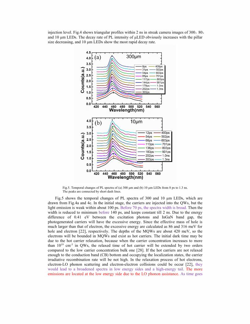
injection level. Fig.4 shows triangular profiles within 2 ns in streak camera images of 300,80,and 10 μm LEDs. The decay rate of PL intensity of μLED obviously increases with the pillar
size decreasing, and 10 μm LEDs show the most rapid decay rate.
Fig.5. Temporal changes of PL spectra of (a) 300 μm and (b) 10 μm LEDs from 8 ps to 1.3 ns.
The peaks are connected by short dash lines.
Fig.5 shows the temporal changes of PL spectra of 300 and 10 μm LEDs, which are
drawn from Fig.4a and 4c. In the initial stage, the carriers are injected into the QWs, but the
light emission is weak within about 100 ps. Before 70 ps, the spectra width is broad. Then the
width is reduced to minimum before 140 ps, and keeps constant till 2 ns. Due to the energy
difference of 0.41 eV between the excitation photons and InGaN band gap, the
photogenerated carriers will have the excessive energy. Since the effective mass of hole is
much larger than that of electron, the excessive energy are calculated as 86 and 316 meV for
hole and electron [22], respectively. The depths of the MQWs are about 420 meV, so the
electrons will be bounded in MQWs and exist as hot carriers. The initial dark time may be
due to the hot carrier relaxation, because when the carrier concentration increases to more
than 1019 cm-3 in QWs, the relaxed time of hot carrier will be extended by two orders
compared to the low carrier concentration bulk one [28]. If the hot carriers are not relaxed
enough to the conduction band (CB) bottom and occupying the localization states, the carrier
irradiative recombination rate will be not high. In the relaxation process of hot electrons,
electron-LO phonon scattering and electron-electron collisions could be occur [22], they
would lead to a broadened spectra in low energy sides and a high-energy tail. The more
emissions are located at the low energy side due to the LO phonon assistance. As time goes

on, the hot carrier concentration decreases, which will lead to blueshift and narrowing of the
spectra. After 140 ps, most of the hot carriers may be relaxed, and the spectral widths become
constant. Because the high carrier concentration is above 1019 cm-3 which would induce the
screening effect and BGR, the specific recombination mechanism will be further explored.
Fig.6. Time resolved (a) peak intensities (b) peak wavelengths of PL spectra are taken from the
streak camera images for 300, 160, 80, 40, 10 μm LEDs with the time scale of 2 ns, and (c) peak
wavelengths of PL spectra with the time scale of 50 ns for 300, 160, 80, 40, 10 μm LEDs .
Time resolved peak intensities and peak wavelengths of PL spectra are taken from the
streak camera images for 300, 160, 80, 40 and 10 μm LEDs, as shown in Fig.6. The time
resolved peak intensities curves in Fig.6a include a rising edge and a falling edge. The rising
edges are terminated at about 140 ps, the slope of the rising edge increases with the size of
μLED decreasing. Correspondingly, the decay rate also increases with the size of μLED
decreasing in the residual time of 2 ns. The exception is the falling edge for 10μm LED, in
which the initial decay rate is slower than those of the other larger size μLEDs, while the
global falling edge decays most rapidly in the time of 2 ns. In Fig.6b, the time resolved peak

wavelengths show blue shift first, and then nearly constant for μLEDs within 2ns, the turning
points are marked by circles. It is obviously that the blue shift is smaller for smaller size
μLEDs, and less shift time as well. But the blue shift of 10 μm LED takes longer time, also as
shown in Fig.5b. The time of 2 ns is too short to show the whole dynamics process of the
photogenerated carriers. Fig.6c shows the peak wavelength change within 50 ns scale. The
peak wavelengths blue shift first before 3.6 ns, and then keep constant for a while, and
red-shift eventually. More clearly, there are trenches at about 3.2 ns for all the μLEDs. By
expanding the time scale in the test, it is found that the blue shift is prolonged. Because the
data are collected under different deflecting voltage in each time scale, the instrument
response will be varied at different time scales. The measured data F(t) are the convolution of
instrument response function (IRF(t)) and real data I(t), where t represents time. It is found
that the counts peaks are usually appeared in the initial 5-8% of the time scale. The spectra
evolution seems prolonged at the initial stage with the time scale increasing. After 5-8% of
the time scale, the data is influenced weakly by instrument response for all time scales.
Although the convolution affects the determination of the accurate time of carrier dynamics,
its process can be observed by the spectra evolution. In a way the evolution with IRF would
provide the time magnification of carrier dynamics, as shown in Fig.6c. It is advantageous to
get more useful information. For example, the trenches are not clear as a brief process at
small time scale while highlighted at larger one.
In order to explain the above results, a model of carrier dynamics is developed referring
to Ref. [26], as shown in Fig.7. The model includes a schematic band diagram and possible
paths of carrier transportation and recombination in InGaN QW in TRPL measurements.
When the laser pulse illuminates the MQWs of μLEDs, photogenerated electrons with excess
energy become hot carriers in the QWs. The localized states are almost empty at this time. As
mentioned above, electron-phonon and electron-electron scattering lead to carrier relaxation
to the states on CB bottom as free carriers. And then free carriers on CB bottom will relax to
the localized states. At the initial time, the carrier concentrations both in CB bottom and
localized states are low, and the recombination at these positions is weak. This is why the
initial PL intensities are weak. Electron-electron, electron-LO phonon interactions in hot
carriers cause the broad spectra and more emission at low energy side. As the hot carriers
concentration decreases, phonon assisted recombination is weakened, and the peak
wavelengths of spectra blue shift, which is shown in Fig. 6b and Fig. 6c. Due to the presence
of free carriers in QWs, BGR happens at this moment, which will hinder carriers relaxation to
low energy level. The compressive strain can enhance the BGR effect in InGaN QWs [23].
The strain will be relaxed when the size of μLEDs decreases, especially for 10μm LEDs.
Thus the small size μLEDs have more free carriers relaxed to the localized states, and the
long wavelength emissions begin playing roles, which lead to the small blue shift in the early
stage in Fig. 6b and Fig.6c. As the hot carriers concentration decreases more, the
concentration of free carriers balances with the localized carriers for a while for small size
μLEDs. So the peak wavelengths of spectra keep constant. When the hot carriers are fully
relaxed, the concentration of free carriers begins to decrease. Then BGR is distinctly
weakened as the free carriers decrease, which will lead to the peak wavelength blue shift.
Less BGR effects cause the localized states filled rapidly, which will lead to the peak
wavelength redshift. Those changes of peak wavelengths like trenches, as shown in Fig. 6c.
The PL intensities increase sharply when the localized states are occupied rapidly. Due to
the less BGR, the transition to localized states is more rapid for smaller size μLEDs [24]. So
the slope of the rising edge increases with the size of μLED decreasing in Fig.6a. The PL
intensities approach their maxima when the sum of the radiative recombination rate for the
localized and free carriers on the CB bottom is largest. These recombination components
make the initial part fall rapidly after the peak intensity. Because the small size μLEDs have a
faster recombination rate for weaker BGR effect, the initial part of the failing edge drops
more rapidly. When the free carriers concentration is reduced further, they would relax to the
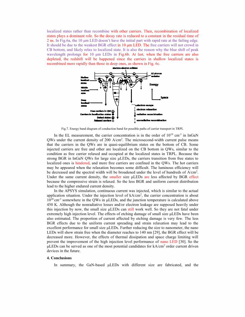
localized states rather than recombine with other carriers. Then, recombination of localized
states plays a dominant role. So the decay rate is reduced to a constant in the residual time of
2 ns. In Fig.6a, the 10 μm LED doesn’t have the initial part with rapid rate at the failing edge.
It should be due to the weakest BGR effect in 10 μm LED. The free carriers will not crowd in
CB bottom, and likely relax to localized state. It is also the reason why the blue shift of peak
wavelength prolongs for 10 μm LEDs in Fig.6b. At last, when the free carriers are also
depleted, the redshift will be happened since the carriers in shallow localized states is
recombined more rapidly than those in deep ones, as shown in Fig. 6c.
Fig.7. Energy band diagram of conduction band for possible paths of carrier transport in TRPL
In the EL measurement, the carrier concentration is in the order of 1019 cm-3 in InGaN
QWs under the current density of 200 A/cm2. The microsecond-width current pulse means
that the carriers in the QWs are in quasi-equilibrium states on the bottom of CB. Some
injected carriers are free and other are localized on the CB bottom in QWs, similar to the
condition as free carrier relaxed and occupied at the localized states in TRPL. Because the
strong BGR in InGaN QWs for large size μLEDs, the carriers transition from free states to
localized ones is hindered, and more free carriers are confined in the QWs. The hot carriers
may be appeared when the relaxation becomes some difficult. The luminous efficiency will
be decreased and the spectral width will be broadened under the level of hundreds of A/cm2.
Under the same current density, the smaller size μLEDs are less affected by BGR effect
because the compressive strain is relaxed. So the less BGR and uniform current distribution
lead to the higher endured current density.
In the APSYS simulation, continuous current was injected, which is similar to the actual
application situation. Under the injection level of kA/cm2, the carrier concentration is about
1020 cm-3 somewhere in the QWs in μLEDs, and the junction temperature is calculated above
450 K. Although the nonradiative losses and/or electron leakage are supposed heavily under
this injection by now, the small size μLEDs can still work well. So they are not fatal under
extremely high injection level. The effects of etching damage of small size μLEDs have been
also estimated. The proportion of current affected by etching damage is very few. The less
BGR effects due to the uniform current spreading and strain relaxation may lead to the
excellent performance for small size μLEDs. Further reducing the size to nanometer, the nano
LEDs will show strain free when the diameter reaches to 140 nm [29], the BGR effect will be
decreased more. However, the effects of thermal dissipation and space charge limiting will
prevent the improvement of the high injection level performance of nano LED [30]. So the
μLEDs can be served as one of the most potential candidates for kA/cm2 order current driven
devices in the future.
4. Conclusions
In summary, the GaN-based μLEDs with different size are fabricated, and the

electroluminescence (EL) measurements stimulated by pulse current are performed on the
different size μLEDs. It is found that tens micron μLEDs can work well under kA/cm2 current
density. Current distributions along the mesa of μLEDs are obtained with the simulations by
the APSYS software package. The current spreading of several tens μLEDs are almost
uniform. But due to the difference of recombination mechanism under high injection level,
the maximum endured current density of the μLEDs of tens micron are quite different. TRPL
measurements show that under high injection level, the smaller size μLEDs have a faster
recombination rate in all wavelength range because of less BGR effect. Therefore, the less
BGR effects may lead to the excellent performance for small size μLEDs, which are due to
the uniform current spreading and strain relaxation.
Acknowledgment
This work was supported by projects of National Key Basic Research Special Foundation of
China under Nos. TG2011CB301905, TG2013CB328705 and Natural Science Foundation of
China under Nos. 61334009, 60876063, 61076012. This work was also supported by
Guangdong Innovative Research Team Program (No. 2009010044).