C500-LDP01-V1 Ladder Program I/O Unitomrondoc.ru/C/W151-E1-3.pdf · Ladder Program I/O Unit...
56
C500-LDP01-V1 Ladder Program I/O Unit Operation Manual Revised January 1992
Transcript of C500-LDP01-V1 Ladder Program I/O Unitomrondoc.ru/C/W151-E1-3.pdf · Ladder Program I/O Unit...
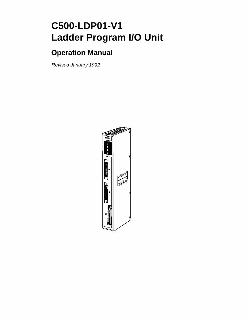
C500-LDP01-V1Ladder Program I/O Unit
Operation Manual
Revised January 1992
�
Notice:OMRON products are manufactured for use according to proper procedures by a qualified operatorand only for the purposes described in this manual.
The following conventions are used to indicate and classify warnings in this manual. Always heed theinformation provided with them.
Caution Indicates information that, if not heeded, could result in minor injury or damageto the product.
DANGER! Indicates information that, if not heeded, could result in loss of life or seriousinjury.
OMRON Product ReferencesAll OMRON products are capitalized in this manual. The word “Unit” is also capitalized when it refersto an OMRON product, regardless of whether or not it appears in the proper name of the product.
The abbreviation “Ch,” which appears in some displays and on some OMRON products, often means“word” and is abbreviated “Wd” in documentation in this sense.
The abbreviation “PC” means Programmable Controller and is not used as an abbreviation for any-thing else.
Visual AidsThe following headings appear in the left column of the manual to help you locate different types ofinformation.
Note Indicates information of particular interest for efficient and convenient operationof the product.
1, 2, 3... 1. Indicates lists of one sort or another, such as procedures, checklists, etc.
OMRON, 1992��� ������ ����� � ���� �� ���� ����������� ��� � ��������� ����� �� � ������ ������ �� ����������� �� ���
����� �� �� ��� ����� ���������� ��������� ������������� ��������� �� �������� ������� �� ����� ������ ������
���� �� ���� �
� ����� ��������� �� ������ ���� ����� �� �� �� �� �� ����������� �������� ����� ������ ����� ���� ��
���������� ������� �� ����� ��� ������������ ��������� �� ����������� �������� �� ���� ������ �� ������ �� �����
������� ������ �� ��������� ��� �� ��!� �� �� ���������� �� ���� ������� ������� ���� ������ ��
������������� ��� ����� �� ���������� ���� �� ��� ��������� ������ ��� ������ �������� ���� �� �� �� �� ��������
���� �������� �� ���� ������������
���
����� � �������
��� �� �
����������� �� � � � � � � � � � � � � � � � � � � � � � � � � � � � � � � � � � � � ���� ������� � � � � � � � � � � � � � � � � � � � � � � � � � � � � � � � � � � � � � � � � � � � � � � � � � � � � � � � � � � � � � � � �
�� � ��� ������������� � � � � � � � � � � � � � � � � � � � � � � � � � � � � � � � � � � � � � � � � � � � � � � � � � � � � � �
��� ��������� ��� ���������� ��� ��� ������������� �� � � � � � � � � � � � � � � � � � � � � � � � � � �
��� ����!"����� �� � � � � � � � � � � � � � � � � � � � � � � � � � � � � � � � � � � � � � � � � � � � � � � � � � � � � � � � � � � �
��� �� �
������������ �� � � � � � � � � � � � � � � � � � � � � � � � � � � � � � � � � � � � ��� ����� ����" �#��!�� ��� ��"�!��� $� � � � � � � � � � � � � � � � � � � � � � � � � � � � � � � � � � � � � � � � � � �
� %�!& ����" �'� �#��!� ��� � � � � � � � � � � � � � � � � � � � � � � � � � � � � � � � � � � � � � � � � � � � � � � � � � � �
��� �� �
���� ����� ��� � � � � � � � � � � � � � � � � � � � � � � � � � � � � � � � � � � � � ���� '( )'������" (�"� * +��� ��� � � � � � � � � � � � � � � � � � � � � � � � � � � � � � � � � � � � � � � � � � � � � � � � � � � �
�� ,��& %�� �-� � � � � � � � � � � � � � � � � � � � � � � � � � � � � � � � � � � � � � � � � � � � � � � � � � � � � � � � � � � � � � �
��� �( )���!��" (�"� * +��� �.� � � � � � � � � � � � � � � � � � � � � � � � � � � � � � � � � � � � � � � � � � � � � � � � � � �
��� /( )/������� (�"� * %�� �.� � � � � � � � � � � � � � � � � � � � � � � � � � � � � � � � � � � � � � � � � � � � � � � � �
��� /� )/����0�������* +��� �.� � � � � � � � � � � � � � � � � � � � � � � � � � � � � � � � � � � � � � � � � � � � � � � � � � �
��$ �1 )���� 1���� * +��� �.� � � � � � � � � � � � � � � � � � � � � � � � � � � � � � � � � � � � � � � � � � � � � � � � � � �
��� ��
���!��""��! ��� � � � � � � � � � � � � � � � � � � � � � � � � � � � � � � � � � � ���� ������� +����� ��� 1���� ����!�� � � � � � � � � � � � � � � � � � � � � � � � � � � � � � � � � � � � � �
�� 2�������� 1��� � � � � � � � � � � � � � � � � � � � � � � � � � � � � � � � � � � � � � � � � � � � � � � � � � � � � � � � � �
��� �������� ��� 2�������� 1��� � � � � � � � � � � � � � � � � � � � � � � � � � � � � � � � � � � � � � � � � � � � � � � �
��� ����������� ��3�!� �� � � � � � � � � � � � � � � � � � � � � � � � � � � � � � � � � � � � � � � � � � � � � � � � � � � � �
��� 2�"��� 2�������� �� � � � � � � � � � � � � � � � � � � � � � � � � � � � � � � � � � � � � � � � � � � � � � � � � � � � � � � �
��� �� �
���!��" �#������� ��"��! �$� � � � � � � � � � � � � � � � � � � � � � � ���� 2�������� �� (4 ��� 12 '/2( 1��� .� � � � � � � � � � � � � � � � � � � � � � � � � � � � � � � � � � � � �
�� �!�� /��� .� � � � � � � � � � � � � � � � � � � � � � � � � � � � � � � � � � � � � � � � � � � � � � � � � � � � � � � � � � � � � � �
��� '����!���� 56�!����� /��� 7� � � � � � � � � � � � � � � � � � � � � � � � � � � � � � � � � � � � � � � � � � � � � � � �
��� '02 (����� /��� �� � � � � � � � � � � � � � � � � � � � � � � � � � � � � � � � � � � � � � � � � � � � � � � � � � � � � � � �
��� �� %
&���������� ��� ����'(��)�����! ��� � � � � � � � � � � � � � � � � �$�� 5���� 1���� ��� /���8"�������� �$� � � � � � � � � � � � � � � � � � � � � � � � � � � � � � � � � � � � � � � � � �
$� 1��������!� �-� � � � � � � � � � � � � � � � � � � � � � � � � � � � � � � � � � � � � � � � � � � � � � � � � � � � � � � � � � � � �
����������+ �������� 1���" �7� � � � � � � � � � � � � � � � � � � � � � � � � � � � � � � � � � � � � � � � � � � � � � � � � � � � � � � � � � � � �
% ���!���!����� ��� � � � � � � � � � � � � � � � � � � � � � � � � � � � � � � � � � � � � � � � � � � � � � � � � � � � � � � � � � � � � � �
� ����������� '����!���� ��� � � � � � � � � � � � � � � � � � � � � � � � � � � � � � � � � � � � � � � � � � � � � � � � � � � � �
� 5���� ��� +��������! �"�� 2�������� ��� � � � � � � � � � � � � � � � � � � � � � � � � � � � � � � � � � � � � � � � � � � � �
���# �$� � � � � � � � � � � � � � � � � � � � � � � � � � � � � � � � � � � � � � � � � � �
�&*�� ��(�� �++���� �,� � � � � � � � � � � � � � � � � � � � � � � � � � � � �
*������� -�����. %�� � � � � � � � � � � � � � � � � � � � � � � � � � � � � � � � �

�#
About this Manual:
This manual describes the installation and operation of the C500-LD01-V1 Ladder Program I/O Unit andincludes the sections described below.
Please read this manual completely and be sure you understand the information provide before attempt-ing to install and operation the Ladder Program I/O Unit.
Section 1 introduces the Unit and describes its components and the way it fits into a PC system. A com-parison of the C500-LD01-V1 and the C500-LD01 is also provided.
Section 2 provides information on switch settings and how certain switch settings affect indicator opera-tion. These switch must be set before mounting and operating the Unit.
Section 3 describes the data areas available for use in programming the Unit.
Section 4 provides information related to programming and operating the Unit. A list of programming in-structions is provided in Appendix C Programming Instructions. Details on programming can be found inthe C500 Operation Manual.
Section 5 describes the scan of the Unit and how the operating mode affects it. It also describes scan timeand I/O response time calculations and provides tables of instruction execution times.
Section 6 provides basic troubleshooting steps, error messages provided by the indicators, and the fusereplacement procedure.
�
��� �� �
�����������
/�� �!���� �������!� ������� ������� ��� ���"�!����� �� ��� ������ ������� '024��� ��� ��!��8� ��# �� ��"��� �� '02
��3�!� ��� ����������� ��3�!�� '� �"� ���3��� � ��8"� ���� ��!��8� �������� ���� �� ��� �� 3����� �� ��� 4��� ���
���3��� ��� ���� ��� "�!����� �� ��� 3����� ���� �� ��� 4����
��� ������� � � � � � � � � � � � � � � � � � � � � � � � � � � � � � � � � � � � � � � � � � � � � � � � � � � � � � � � � � � � � � � � �
�� � ��� ������������� � � � � � � � � � � � � � � � � � � � � � � � � � � � � � � � � � � � � � � � � � � � � � � � � � � � � � �
��� ��������� ��� ���������� ��� ��� ������������� �� � � � � � � � � � � � � � � � � � � � � � � � � � �
��� ����!"����� �� � � � � � � � � � � � � � � � � � � � � � � � � � � � � � � � � � � � � � � � � � � � � � � � � � � � � � � � � � � �
�
1-1 FeaturesThe C500-LDP01-V1 Ladder Program I/O Unit executes a ladder program tocontrol external I/O independently of the PC. The ladder program contained inthe Unit is written by the user.
The C500-LDP01-V1 Ladder Program I/O Unit can be used with the followingSYSMAC C-series PCs: C500, C1000H, C2000H.
Applications Examples• External I/O can be controlled by the Ladder Program I/O Unit instead of the
PC.
• The Ladder Program I/O Unit can be used as a timer.
• The Ladder Program I/O Unit can be used as a high-speed input unit.
• By controlling external inputs and outputs, the Ladder Program I/O Unit canreduce the processing load handled by the PC.
C500 Instructions The Ladder Program I/O Unit uses the same instructions as the C500, so ladderprograms can be constructed in the same way. A total of 49 different instructionsis available. (Not all C500 instructions are supported.)
The 16 DC inputs and 16 transistor outputs can be connected to external I/O de-vices so the Unit can be used as for normal I/O operation. Of the 16 DC inputs, 8inputs (2 groups of 4) can be set for high-speed inputs with a minimum pulsewidth of 0.5 ms, so inputs shorter than the scan time can be detected.
The Unit connects to the PC through 16 input points and 16 output points, socontrol signals can be passed back and forth between the PC and the Unit. Fur-thermore, when the I/O WRITE and I/O READ (WRIT(87)/READ(88)) instruc-tions are executed in the PC program, up to 32 words of data can be transferredto or from the Unit.
Built-in Realtime Clock A realtime clock is built into the Unit, so it can act as a timer and manage I/Otiming.
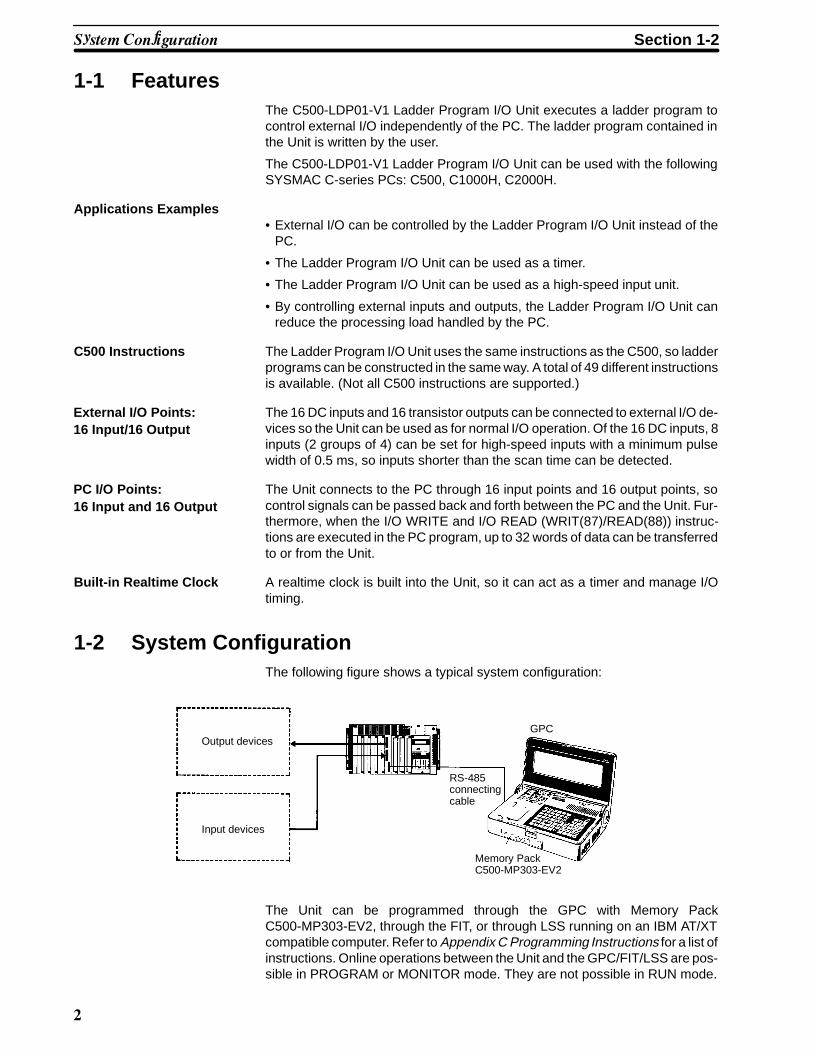
1-2 System ConfigurationThe following figure shows a typical system configuration:
RS-485connectingcable
GPC
Memory PackC500-MP303-EV2
Output devices
Input devices
The Unit can be programmed through the GPC with Memory PackC500-MP303-EV2, through the FIT, or through LSS running on an IBM AT/XTcompatible computer. Refer to Appendix C Programming Instructions for a list ofinstructions. Online operations between the Unit and the GPC/FIT/LSS are pos-sible in PROGRAM or MONITOR mode. They are not possible in RUN mode.
External I/O Points:16 Input/16 Output
PC I/O Points:16 Input and 16 Output
������ ���� ����� Section 1-2
�
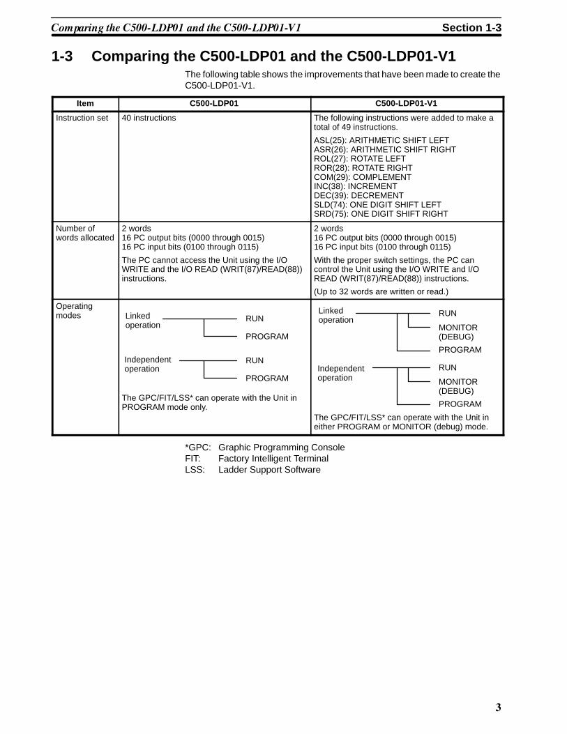
1-3 Comparing the C500-LDP01 and the C500-LDP01-V1The following table shows the improvements that have been made to create theC500-LDP01-V1.
Item C500-LDP01 C500-LDP01-V1
Instruction set 40 instructions The following instructions were added to make atotal of 49 instructions.
ASL(25): ARITHMETIC SHIFT LEFTASR(26): ARITHMETIC SHIFT RIGHTROL(27): ROTATE LEFTROR(28): ROTATE RIGHTCOM(29): COMPLEMENTINC(38): INCREMENTDEC(39): DECREMENTSLD(74): ONE DIGIT SHIFT LEFTSRD(75): ONE DIGIT SHIFT RIGHT
Number ofwords allocated
2 words16 PC output bits (0000 through 0015)16 PC input bits (0100 through 0115)
The PC cannot access the Unit using the I/OWRITE and the I/O READ (WRIT(87)/READ(88))instructions.
2 words16 PC output bits (0000 through 0015)16 PC input bits (0100 through 0115)
With the proper switch settings, the PC cancontrol the Unit using the I/O WRITE and I/OREAD (WRIT(87)/READ(88)) instructions.
(Up to 32 words are written or read.)
Operatingmodes Linked
operationRUN
PROGRAM
Independentoperation
RUN
PROGRAM
The GPC/FIT/LSS* can operate with the Unit inPROGRAM mode only.
Linkedoperation
RUN
PROGRAM
Independentoperation
MONITOR(DEBUG)
RUN
PROGRAM
MONITOR(DEBUG)
The GPC/FIT/LSS* can operate with the Unit ineither PROGRAM or MONITOR (debug) mode.
*GPC: Graphic Programming ConsoleFIT: Factory Intelligent TerminalLSS: Ladder Support Software
�������� ��� ���������� �� ��� ������������� Section 1-3

1-4 Nomenclature
Indicators
SwitchesRemove the display windowto access the switches.
Output connectorsConnector for transistor outputs.(Use connector provided.)
Input connectorConnector for 24 VDC power supply input.(Use connector provided.)
RS-485 interface connectorConnector for the GPC, FIT, orLSS. Use one of the followingcables:
3G2A2-CN221 (2 m)C500-CN523 (5 m)C500-CN131 (10 m)C500-CN231 (20 m)C500-CN331 (30 m)C500-CN431 (40 m)C500-CN531 (50 m)
Mounting screw
Backplane connector
DIP Switch
Mounting screw
Front Panel Back Panel
�������� �� Section 1-4

�
��� �� �
������������
/�� �!������!��8� ��� #��!� ������ ��9���������� �� ����������/�������������4��� ����!����:#��!� ��� !�����""�� 8
� #��!� ������: � �"� ��!��8���
�� ����� ����" �#��!�� ��� ��"�!��� $� � � � � � � � � � � � � � � � � � � � � � � � � � � � � � � � � � � � � � � � � � �
� %�!& ����" �'� �#��!� ��� � � � � � � � � � � � � � � � � � � � � � � � � � � � � � � � � � � � � � � � � � � � � � � � � � � �

%
2-1 Front Panel Switches and SelectorsSwitch/Selector Location Remove the display window using a standard screwdriver to access the
switches and selectors shown below.
Standardscrewdriver
Reset switch (SW2)Indicator selector (SW3)
Mode selector (SW4)Mode switch (SW5)
Switch/Selector Functions
SwitchNo.
Designation Function
SW 2 Reset switch The Unit can be reset and restarted by pressing the reset switch.
Note Resetting the Unit completely clears I/O bit status and data memory.
If the back panel DIP switch is set for PC-linked operation, the Unit will enter RUN orPROGRAM mode after resetting, depending on the status of the PC. If the back panelDIP switch is set for independent operation, the Unit will enter RUN, MONITOR (debug),or PROGRAM mode, depending on the setting of SW4. The same process occurs whenthe power is turned on.
SW 3 Displayselector
Select indicator operation with this selector. Refer to the following pages for details.
SW 4 Mode selector Changing this selector followed by pressing and releasing SW5 will alter the operatingmode as shown below. This switch also determines the mode entered when power isturned on or the Unit is reset.
SW 4 set to up position RUN. . . . .SW 4 set to center MONITOR (debug). . . . . . . .SW 4 set to down position PROGRAM. .
SW 5 Mode switch When this switch is pressed and released, the Unit will enter the mode set on SW4. Theoperation of this switch is enabled by turning on pin 5 of the back panel DIP switch, anddisabled by turning off pin 5.
The Unit cannot be switched to RUN or MONITOR mode when the program is beingtransferred from a Programming Device or an error has occurred.
���� ���� �������� �� ��������� Section 2-1
$
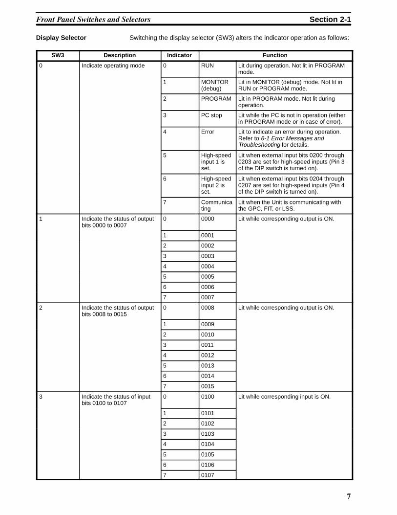
Display Selector Switching the display selector (SW3) alters the indicator operation as follows:
SW3 Description Indicator Function
0 Indicate operating mode 0 RUN Lit during operation. Not lit in PROGRAMmode.
1 MONITOR(debug)
Lit in MONITOR (debug) mode. Not lit inRUN or PROGRAM mode.
2 PROGRAM Lit in PROGRAM mode. Not lit duringoperation.
3 PC stop Lit while the PC is not in operation (eitherin PROGRAM mode or in case of error).
4 Error Lit to indicate an error during operation.Refer to 6-1 Error Messages andTroubleshooting for details.
5 High-speedinput 1 isset.
Lit when external input bits 0200 through0203 are set for high-speed inputs (Pin 3of the DIP switch is turned on).
6 High-speedinput 2 isset.
Lit when external input bits 0204 through0207 are set for high-speed inputs (Pin 4of the DIP switch is turned on).
7 Communicating
Lit when the Unit is communicating withthe GPC, FIT, or LSS.
1 Indicate the status of outputbits 0000 to 0007
0 0000 Lit while corresponding output is ON.
1 0001
2 0002
3 0003
4 0004
5 0005
6 0006
7 0007
2 Indicate the status of outputbits 0008 to 0015
0 0008 Lit while corresponding output is ON.
1 0009
2 0010
3 0011
4 0012
5 0013
6 0014
7 0015
3 Indicate the status of inputbits 0100 to 0107
0 0100 Lit while corresponding input is ON.
1 0101
2 0102
3 0103
4 0104
5 0105
6 0106
7 0107
���� ���� �������� �� ��������� Section 2-1
/
SW3 FunctionIndicatorDescription
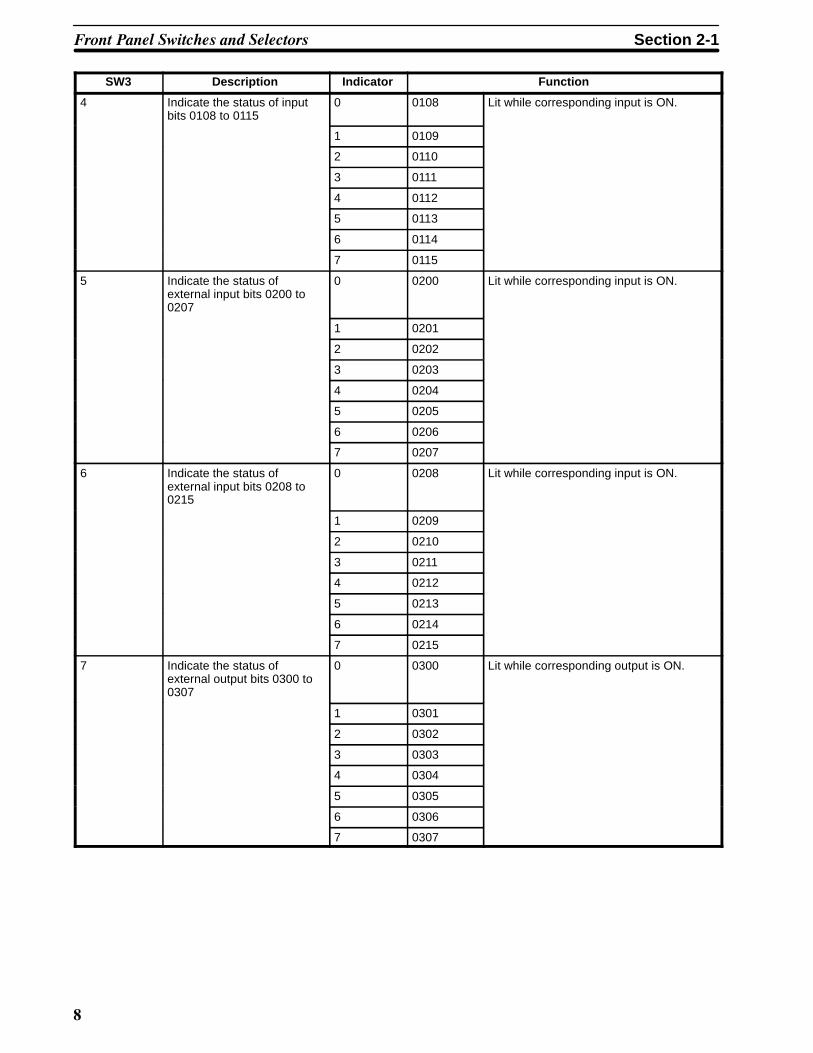
4 Indicate the status of inputbits 0108 to 0115
0 0108 Lit while corresponding input is ON.
1 0109
2 0110
3 0111
4 0112
5 0113
6 0114
7 0115
5 Indicate the status ofexternal input bits 0200 to0207
0 0200 Lit while corresponding input is ON.
1 0201
2 0202
3 0203
4 0204
5 0205
6 0206
7 0207
6 Indicate the status ofexternal input bits 0208 to0215
0 0208 Lit while corresponding input is ON.
1 0209
2 0210
3 0211
4 0212
5 0213
6 0214
7 0215
7 Indicate the status ofexternal output bits 0300 to0307
0 0300 Lit while corresponding output is ON.
1 0301
2 0302
3 0303
4 0304
5 0305
6 0306
7 0307
���� ���� �������� �� ��������� Section 2-1
,
SW3 FunctionIndicatorDescription
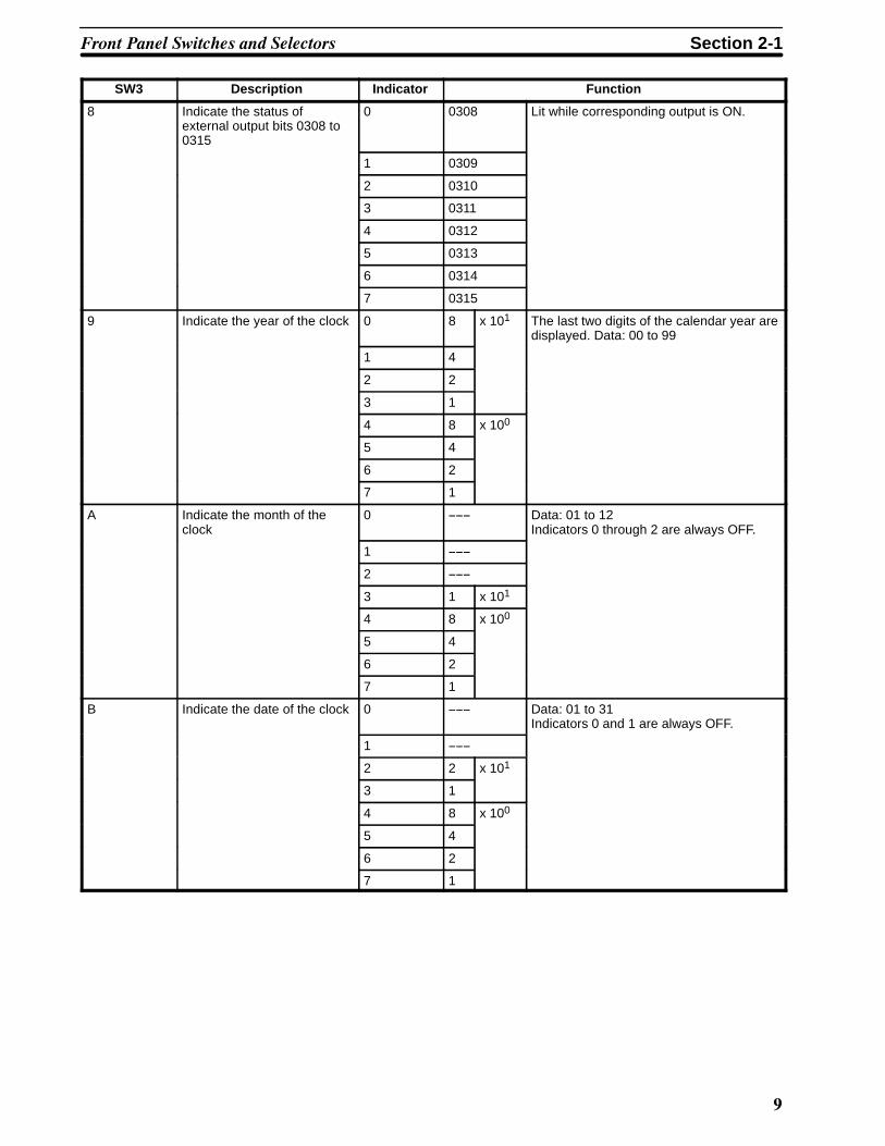
8 Indicate the status ofexternal output bits 0308 to0315
0 0308 Lit while corresponding output is ON.
1 0309
2 0310
3 0311
4 0312
5 0313
6 0314
7 0315
9 Indicate the year of the clock 0 8 x 101 The last two digits of the calendar year aredisplayed. Data: 00 to 99
1 4
2 2
3 1
4 8 x 100
5 4
6 2
7 1
A Indicate the month of theclock
0 ------ Data: 01 to 12Indicators 0 through 2 are always OFF.
1 ------
2 ------
3 1 x 101
4 8 x 100
5 4
6 2
7 1
B Indicate the date of the clock 0 ------ Data: 01 to 31Indicators 0 and 1 are always OFF.
1 ------
2 2 x 101
3 1
4 8 x 100
5 4
6 2
7 1
���� ���� �������� �� ��������� Section 2-1

�0
SW3 FunctionIndicatorDescription
C Indicate the hour of the clock 0 ------ Data: 00 to 23 (24-hour clock)Indicators 0 and 1 are always OFF.
1 ------
2 2 x 101
3 1
4 8 x 100
5 4
6 2
7 1
D Indicate the minutes of theclock
0 ------ Data: 00 to 59 (minutes)Indicator 0 is always OFF.
1 4 x 101
2 2
3 1
4 8 x 100
5 4
6 2
7 1
E Indicate the seconds of theclock
0 ------ Data: 00 to 59 (seconds)Indicator 0 is always OFF.
1 4 x 101
2 2
3 1
4 8 x 100
5 4
6 2
7 1
F Indicate the day of the week 0 ------ Data: 00 to 06Indicators 0 through 4 are always OFF.
1 ------ 00: Sunday; 01: Monday; 02: Tuesday;
2 ------ 03: Wednesday; 04: Thursday; 05: Friday;
3 ------ 06: Saturday
4 ------
5 4 x 100
6 2
7 1
���� ���� �������� �� ��������� Section 2-1
��
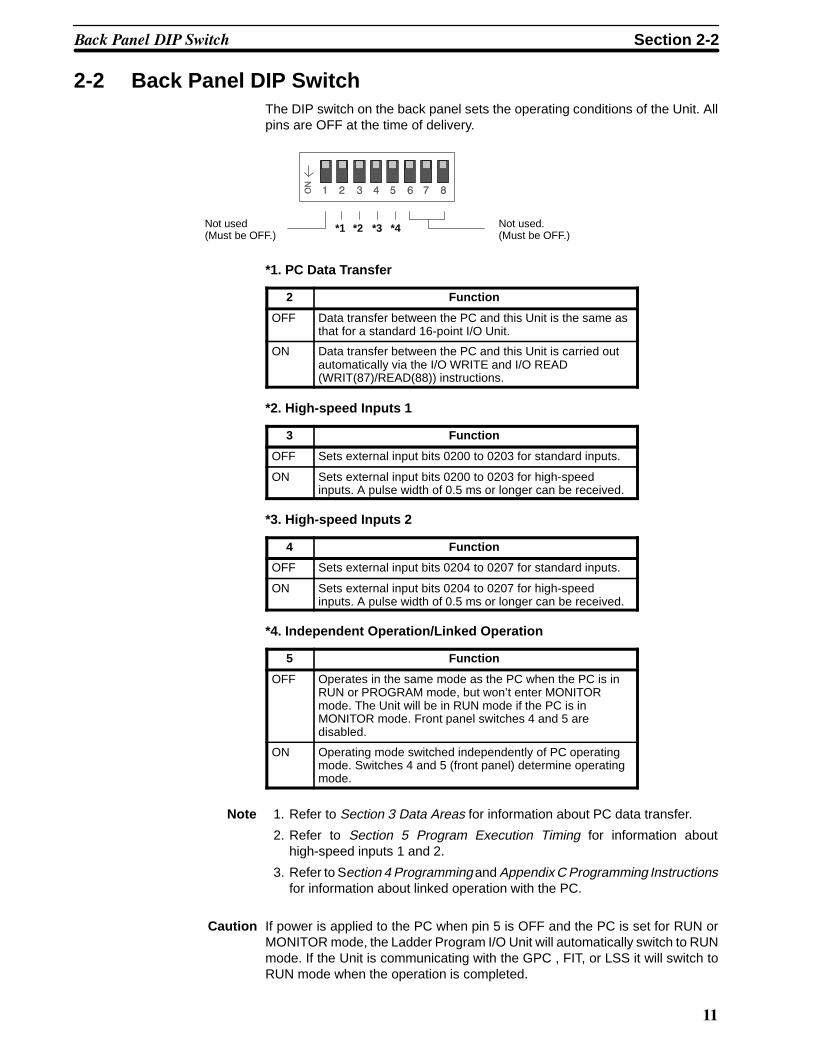
2-2 Back Panel DIP SwitchThe DIP switch on the back panel sets the operating conditions of the Unit. Allpins are OFF at the time of delivery.
*2 *3 *4 Not used.(Must be OFF.)
Not used(Must be OFF.)
*1
*1. PC Data Transfer
2 Function
OFF Data transfer between the PC and this Unit is the same asthat for a standard 16-point I/O Unit.
ON Data transfer between the PC and this Unit is carried outautomatically via the I/O WRITE and I/O READ(WRIT(87)/READ(88)) instructions.
*2. High-speed Inputs 1
3 Function
OFF Sets external input bits 0200 to 0203 for standard inputs.
ON Sets external input bits 0200 to 0203 for high-speedinputs. A pulse width of 0.5 ms or longer can be received.
*3. High-speed Inputs 2
4 Function
OFF Sets external input bits 0204 to 0207 for standard inputs.
ON Sets external input bits 0204 to 0207 for high-speedinputs. A pulse width of 0.5 ms or longer can be received.
*4. Independent Operation/Linked Operation
5 Function
OFF Operates in the same mode as the PC when the PC is inRUN or PROGRAM mode, but won’t enter MONITORmode. The Unit will be in RUN mode if the PC is inMONITOR mode. Front panel switches 4 and 5 aredisabled.
ON Operating mode switched independently of PC operatingmode. Switches 4 and 5 (front panel) determine operatingmode.
Note 1. Refer to Section 3 Data Areas for information about PC data transfer.
2. Refer to Section 5 Program Execution Timing for information abouthigh-speed inputs 1 and 2.
3. Refer to Section 4 Programming and Appendix C Programming Instructionsfor information about linked operation with the PC.
Caution If power is applied to the PC when pin 5 is OFF and the PC is set for RUN orMONITOR mode, the Ladder Program I/O Unit will automatically switch to RUNmode. If the Unit is communicating with the GPC , FIT, or LSS it will switch toRUN mode when the operation is completed.
��! ���� �"� ������ Section 2-2
��
��� �� �
���� �����
/�� �!���� ��!��8� ��� ���� ���� �3��"�8"� ��� �� �� ������������ /�� �� �� ��� '02(5+���� '02,('/5 �����!������� �"� ��!��8���
��� '( )'������" (�"� * +��� ��� � � � � � � � � � � � � � � � � � � � � � � � � � � � � � � � � � � � � � � � � � � � � � � � � � � �
����� ����" '02 2�������� ��� � � � � � � � � � � � � � � � � � � � � � � � � � � � � � � � � � � � � � � � � � � � � �
���� 2�������� 3�� ,('/).-*0(5+�)..* �$� � � � � � � � � � � � � � � � � � � � � � � � � � � � � � � � � � �
�� ,��& %�� �-� � � � � � � � � � � � � � � � � � � � � � � � � � � � � � � � � � � � � � � � � � � � � � � � � � � � � � � � � � � � � � �
��� �( )���!��" (�"� * +��� �.� � � � � � � � � � � � � � � � � � � � � � � � � � � � � � � � � � � � � � � � � � � � � � � � � � �
��� /( )/������� (�"� * %�� �.� � � � � � � � � � � � � � � � � � � � � � � � � � � � � � � � � � � � � � � � � � � � � � � � �
��� /� )/����0�������* +��� �.� � � � � � � � � � � � � � � � � � � � � � � � � � � � � � � � � � � � � � � � � � � � � � � � � � �
��$ �1 )���� 1���� * +��� �.� � � � � � � � � � � � � � � � � � � � � � � � � � � � � � � � � � � � � � � � � � � � � � � � � � �
�
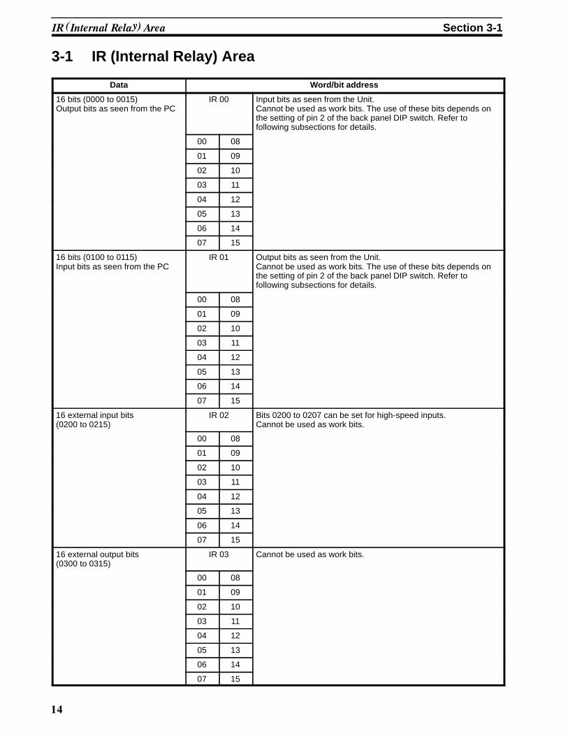
3-1 IR (Internal Relay) Area
Data Word/bit address
16 bits (0000 to 0015)Output bits as seen from the PC
IR 00 Input bits as seen from the Unit.Cannot be used as work bits. The use of these bits depends onthe setting of pin 2 of the back panel DIP switch. Refer tofollowing subsections for details.
00 08
01 09
02 10
03 11
04 12
05 13
06 14
07 15
16 bits (0100 to 0115)Input bits as seen from the PC
IR 01 Output bits as seen from the Unit.Cannot be used as work bits. The use of these bits depends onthe setting of pin 2 of the back panel DIP switch. Refer tofollowing subsections for details.
00 08
01 09
02 10
03 11
04 12
05 13
06 14
07 15
16 external input bits(0200 to 0215)
IR 02 Bits 0200 to 0207 can be set for high-speed inputs.Cannot be used as work bits.
00 08
01 09
02 10
03 11
04 12
05 13
06 14
07 15
16 external output bits(0300 to 0315)
IR 03 Cannot be used as work bits.
00 08
01 09
02 10
03 11
04 12
05 13
06 14
07 15
"# $"����� #����% &��� Section 3-1
��
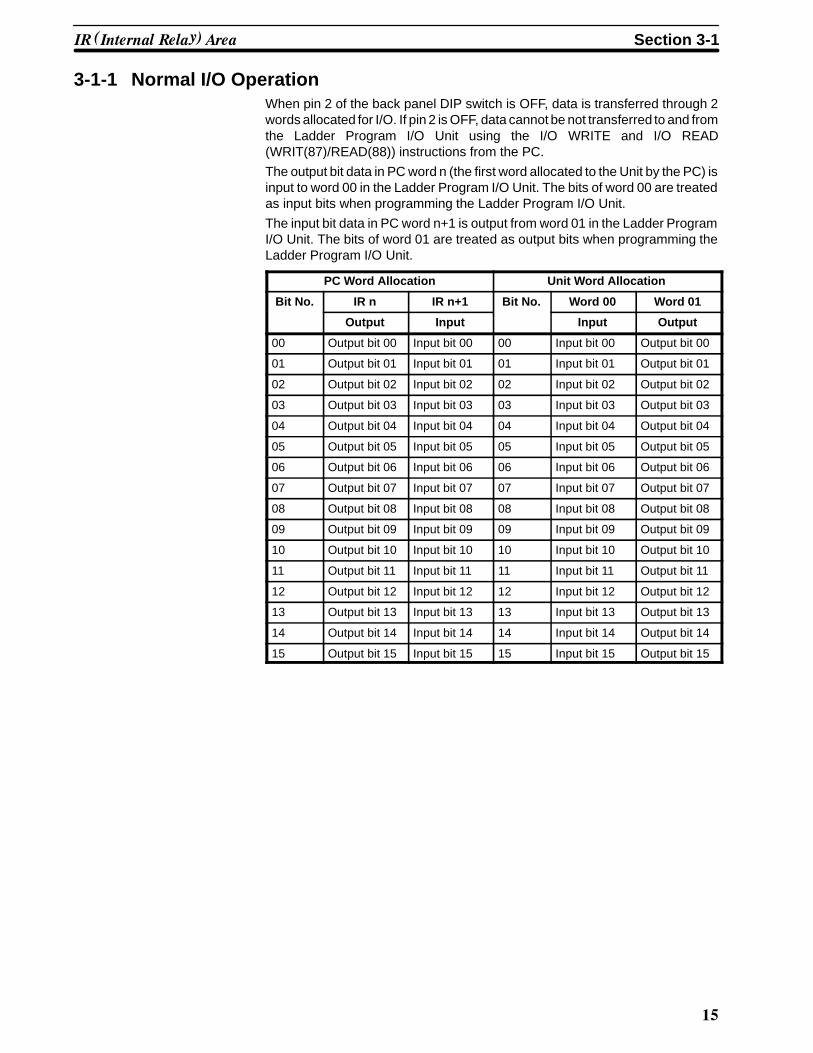
3-1-1 Normal I/O OperationWhen pin 2 of the back panel DIP switch is OFF, data is transferred through 2words allocated for I/O. If pin 2 is OFF, data cannot be not transferred to and fromthe Ladder Program I/O Unit using the I/O WRITE and I/O READ(WRIT(87)/READ(88)) instructions from the PC.
The output bit data in PC word n (the first word allocated to the Unit by the PC) isinput to word 00 in the Ladder Program I/O Unit. The bits of word 00 are treatedas input bits when programming the Ladder Program I/O Unit.
The input bit data in PC word n+1 is output from word 01 in the Ladder ProgramI/O Unit. The bits of word 01 are treated as output bits when programming theLadder Program I/O Unit.
PC Word Allocation Unit Word Allocation
Bit No. IR n IR n+1 Bit No. Word 00 Word 01
Output Input Input Output
00 Output bit 00 Input bit 00 00 Input bit 00 Output bit 00
01 Output bit 01 Input bit 01 01 Input bit 01 Output bit 01
02 Output bit 02 Input bit 02 02 Input bit 02 Output bit 02
03 Output bit 03 Input bit 03 03 Input bit 03 Output bit 03
04 Output bit 04 Input bit 04 04 Input bit 04 Output bit 04
05 Output bit 05 Input bit 05 05 Input bit 05 Output bit 05
06 Output bit 06 Input bit 06 06 Input bit 06 Output bit 06
07 Output bit 07 Input bit 07 07 Input bit 07 Output bit 07
08 Output bit 08 Input bit 08 08 Input bit 08 Output bit 08
09 Output bit 09 Input bit 09 09 Input bit 09 Output bit 09
10 Output bit 10 Input bit 10 10 Input bit 10 Output bit 10
11 Output bit 11 Input bit 11 11 Input bit 11 Output bit 11
12 Output bit 12 Input bit 12 12 Input bit 12 Output bit 12
13 Output bit 13 Input bit 13 13 Input bit 13 Output bit 13
14 Output bit 14 Input bit 14 14 Input bit 14 Output bit 14
15 Output bit 15 Input bit 15 15 Input bit 15 Output bit 15
"# $"����� #����% &��� Section 3-1

�%
3-1-2 Operation via WRIT(87)/READ(88)
When pin 2 of the back panel DIP switch is ON, data can be transferred to andfrom the Ladder Program I/O Unit using the I/O WRITE and I/O READ(WRIT(87)/READ(88)) instructions from the PC. WRIT(87) and READ(88) areused automatically for this data transfer in the Ladder Program I/O Unit and arenot available for user programming except in the PC. The Ladder Program I/OUnit must be mounted to the CPU Rack or Expansion I/O Rack of a PC that sup-ports WRIT(87)/READ(88).
Data written by the WRIT(87) instruction in the PC program is stored in DM 064through DM 095 in the Unit. A maximum of 32 words can be transferred. Dataread by the READ(88) instruction in the PC is stored in DM 096 through DM 127.A maximum of 32 words of data can be read. The bits in parentheses are con-trolled automatically (as described below) when WRIT(87)/READ(88) are en-abled. Treat these as read-only bits. The other input and output bits shown be-low can be used as normal I/O bits.
Do not output to word n with the MOV(21) instruction in the PC program. Whenoutputting to word n, set the PC Busy, PC Write Completed, and PC Read Com-pleted Flags to 0 (OFF). Also, do not output to word 01 with the MOV(21) instruc-tion in the Ladder Program I/O Unit program. When outputting to word 01, set theI/O Busy, I/O Read End, I/O Write End, I/O Read OK, and I/O Write OK Flags to 0(OFF).
Bit 0103 (the I/O Read OK Flag) is turned ON when data has been transferredcorrectly with the WRIT(87) instruction. It remains ON until the WRIT(87) in-struction is executed again. Bit 0104 (the I/O Write OK Flag) is turned ON whendata has been written from the Ladder Program I/O Unit. It is turned OFF whenthe READ(88) instruction is executed in the PC.
PC Word Allocation Unit Word Allocation
Bit No. IR n IR n+1 Bit No. Word 00 Word 01
Output Input Input Output
00 (PC Busy) (I/O Busy) 00 (PC Busy) (I/O Busy)
01 (PC WriteComplete)
(I/O ReadEnd)
01 (PC WriteComplete)
(I/O ReadEnd)
02 (PC ReadComplete)
(I/O WriteEnd)
02 (PC ReadComplete)
(I/O WriteEnd)
03 Output bit 03 (I/O Read Ok) 03 Input bit 03 (I/O Read Ok)
04 Output bit 04 (I/O Write Ok) 04 Input bit 04 (I/O Write Ok)
05 Output bit 05 Input bit 05 05 Input bit 05 Output bit 05
06 Output bit 06 Input bit 06 06 Input bit 06 Output bit 06
07 Output bit 07 Input bit 07 07 Input bit 07 Output bit 07
08 Output bit 08 Input bit 08 08 Input bit 08 Output bit 08
09 Output bit 09 Input bit 09 09 Input bit 09 Output bit 09
10 Output bit 10 Input bit 10 10 Input bit 10 Output bit 10
11 Output bit 11 Input bit 11 11 Input bit 11 Output bit 11
12 Output bit 12 Input bit 12 12 Input bit 12 Output bit 12
13 Output bit 13 Input bit 13 13 Input bit 13 Output bit 13
14 Output bit 14 Input bit 14 14 Input bit 14 Output bit 14
15 Output bit 15 Input bit 15 15 Input bit 15 Output bit 15
"# $"����� #����% &��� Section 3-1
�$
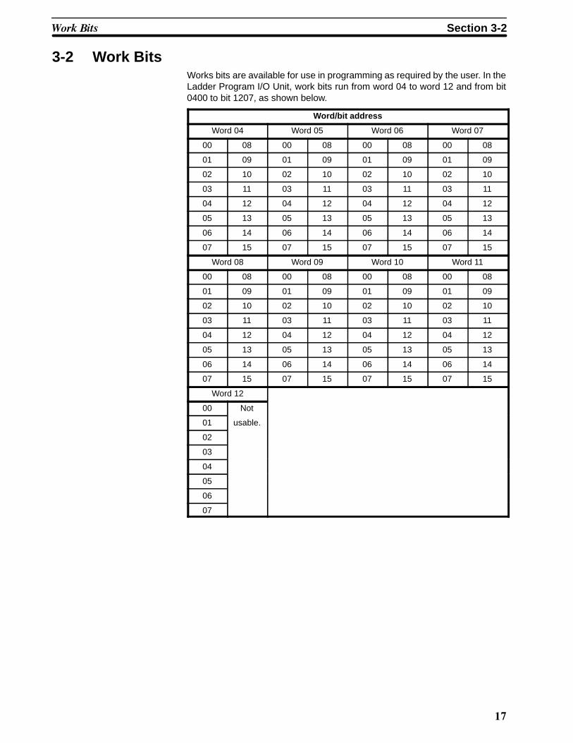
3-2 Work BitsWorks bits are available for use in programming as required by the user. In theLadder Program I/O Unit, work bits run from word 04 to word 12 and from bit0400 to bit 1207, as shown below.
Word/bit address
Word 04 Word 05 Word 06 Word 07
00 08 00 08 00 08 00 08
01 09 01 09 01 09 01 09
02 10 02 10 02 10 02 10
03 11 03 11 03 11 03 11
04 12 04 12 04 12 04 12
05 13 05 13 05 13 05 13
06 14 06 14 06 14 06 14
07 15 07 15 07 15 07 15
Word 08 Word 09 Word 10 Word 11
00 08 00 08 00 08 00 08
01 09 01 09 01 09 01 09
02 10 02 10 02 10 02 10
03 11 03 11 03 11 03 11
04 12 04 12 04 12 04 12
05 13 05 13 05 13 05 13
06 14 06 14 06 14 06 14
07 15 07 15 07 15 07 15
Word 12
00 Not
01 usable.
02
03
04
05
06
07
'��! ��� Section 3-2
�/
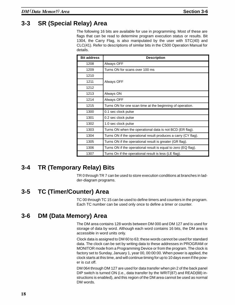
3-3 SR (Special Relay) AreaThe following 16 bits are available for use in programming. Most of these areflags that can be read to determine program execution status or results. Bit1304, the Carry Flag, is also manipulated by the user with STC(40) andCLC(41). Refer to descriptions of similar bits in the C500 Operation Manual fordetails.
Bit address Description
1208 Always OFF
1209 Turns ON for scans over 100 ms
1210
1211 Always OFF
1212
1213 Always ON
1214 Always OFF
1215 Turns ON for one scan time at the beginning of operation.
1300 0.1 sec clock pulse
1301 0.2 sec clock pulse
1302 1.0 sec clock pulse
1303 Turns ON when the operational data is not BCD (ER flag).
1304 Turns ON if the operational result produces a carry (CY flag).
1305 Turns ON if the operational result is greater (GR flag).
1306 Turns ON if the operational result is equal to zero (EQ flag).
1307 Turns On if the operational result is less (LE flag).
3-4 TR (Temporary Relay) BitsTR 0 through TR 7 can be used to store execution conditions at branches in lad-der-diagram programs.
3-5 TC (Timer/Counter) AreaTC 00 through TC 15 can be used to define timers and counters in the program.Each TC number can be used only once to define a timer or counter.
3-6 DM (Data Memory) AreaThe DM area contains 128 words between DM 000 and DM 127 and is used forstorage of data by word. Although each word contains 16 bits, the DM area isaccessible in word units only.
Clock data is assigned to DM 60 to 63; these words cannot be used for standarddata. The clock can be set by writing data to these addresses in PROGRAM orMONITOR mode from a Programming Device or from the program. The clock isfactory set to Sunday, January 1, year 00, 00:00:00. When power is applied, theclock starts at this time, and will continue timing for up to 10 days even if the pow-er is cut off.
DM 064 through DM 127 are used for data transfer when pin 2 of the back panelDIP switch is turned ON (i.e., data transfer by the WRIT(87) and READ(88) in-structions is enabled), and this region of the DM area cannot be used as normalDM words.
�( $���� (�����% &��� Section 3-6
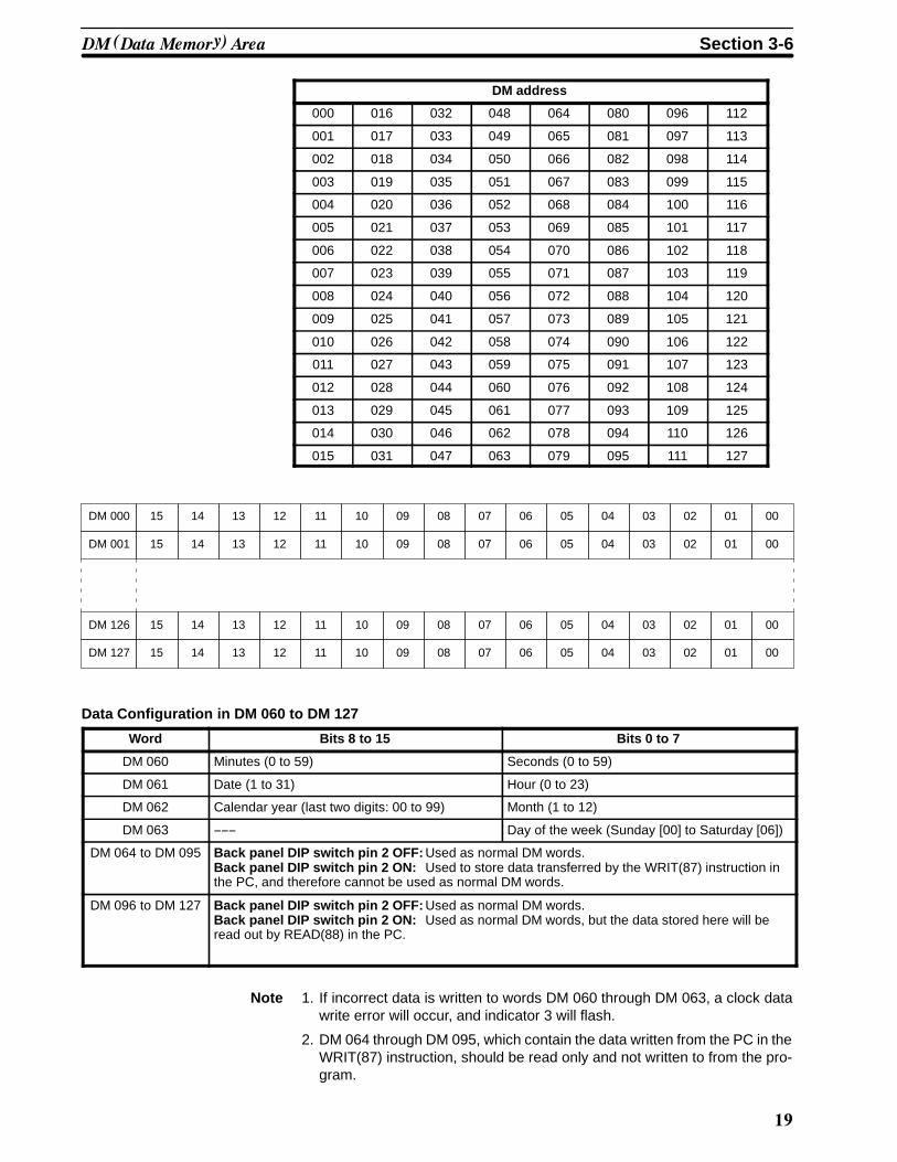
�,
DM address
000 016 032 048 064 080 096 112
001 017 033 049 065 081 097 113
002 018 034 050 066 082 098 114
003 019 035 051 067 083 099 115
004 020 036 052 068 084 100 116
005 021 037 053 069 085 101 117
006 022 038 054 070 086 102 118
007 023 039 055 071 087 103 119
008 024 040 056 072 088 104 120
009 025 041 057 073 089 105 121
010 026 042 058 074 090 106 122
011 027 043 059 075 091 107 123
012 028 044 060 076 092 108 124
013 029 045 061 077 093 109 125
014 030 046 062 078 094 110 126
015 031 047 063 079 095 111 127
15 14 13 12 11 10 09 08 07 06 05 04 03 02 01 00DM 000
DM 001
DM 126
DM 127
15 14 13 12 11 10 09 08 07 06 05 04 03 02 01 00
15 14 13 12 11 10 09 08 07 06 05 04 03 02 01 00
15 14 13 12 11 10 09 08 07 06 05 04 03 02 01 00
Data Configuration in DM 060 to DM 127
Word Bits 8 to 15 Bits 0 to 7
DM 060 Minutes (0 to 59) Seconds (0 to 59)
DM 061 Date (1 to 31) Hour (0 to 23)
DM 062 Calendar year (last two digits: 00 to 99) Month (1 to 12)
DM 063 ------ Day of the week (Sunday [00] to Saturday [06])
DM 064 to DM 095 Back panel DIP switch pin 2 OFF: Used as normal DM words.Back panel DIP switch pin 2 ON: Used to store data transferred by the WRIT(87) instruction inthe PC, and therefore cannot be used as normal DM words.
DM 096 to DM 127 Back panel DIP switch pin 2 OFF: Used as normal DM words.Back panel DIP switch pin 2 ON: Used as normal DM words, but the data stored here will beread out by READ(88) in the PC.
Note 1. If incorrect data is written to words DM 060 through DM 063, a clock datawrite error will occur, and indicator 3 will flash.
2. DM 064 through DM 095, which contain the data written from the PC in theWRIT(87) instruction, should be read only and not written to from the pro-gram.
�( $���� (�����% &��� Section 3-6
��
��� ��
���!��""��!
/�� �!���� ��!��8� ��� ����������� ��������� ���8"� ���� ��� ����������� ��3�!� ��� ��� ��������� �����,����
��� ��� ������� � 8��!�"" ��� ����#������ � ������� ��� �����: �6!��� ���� ��� �����!���� �� � � 8�� ��""�� ��� ��� ����
���� ������� (���� �� �������������� ����� ��� �����" ��#������ ��� ���������� �������������������� �������
��� ��� ��� �����!���� �� ���� !�� 8� ��� #��� ��� 4����
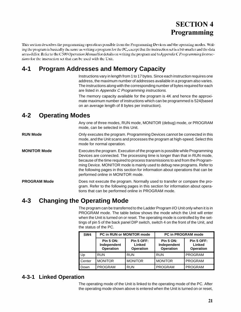
4-1 Program Addresses and Memory CapacityInstructions vary in length from 1 to 17 bytes. Since each instruction requires oneaddress, the maximum number of addresses available in a program also varies.The instructions along with the corresponding number of bytes required for eachare listed in Appendix C Programming instructions.
The memory capacity available for the program is 4K and hence the approxi-mate maximum number of instructions which can be programmed is 524(basedon an average length of 8 bytes per instruction).
4-2 Operating ModesAny one of three modes, RUN mode, MONITOR (debug) mode, or PROGRAMmode, can be selected in this Unit.
RUN Mode Only executes the program. Programming Devices cannot be connected in thismode, and the Unit scans and processes the program at high-speed. Select thismode for normal operation.
MONITOR Mode Executes the program. Execution of the program is possible while ProgrammingDevices are connected. The processing time is longer than that in RUN mode,because of the time required to process transmissions to and from the Program-ming Device. MONITOR mode is mainly used to debug new programs. Refer tothe following pages in this section for information about operations that can beperformed online in MONITOR mode.
PROGRAM Mode Does not execute the program. Normally used to transfer or compare the pro-gram. Refer to the following pages in this section for information about opera-tions that can be performed online in PROGRAM mode.
4-3 Changing the Operating ModeThe program can be transferred to the Ladder Program I/O Unit only when it is inPROGRAM mode. The table below shows the mode which the Unit will enterwhen the Unit is turned on or reset. The operating mode is controlled by the set-tings of pin 5 of the back panel DIP switch, switch 4 on the front of the Unit, andthe status of the PC.
SW4 PC in RUN or MONITOR mode PC in PROGRAM mode
Pin 5 ON:Independent
Operation
Pin 5 OFF:Linked
Operation
Pin 5 ON:Independent
Operation
Pin 5 OFF:Linked
Operation
Up RUN RUN RUN PROGRAM
Center MONITOR MONITOR MONITOR PROGRAM
Down PROGRAM RUN PROGRAM PROGRAM
4-3-1 Linked OperationThe operating mode of the Unit is linked to the operating mode of the PC. Afterthe operating mode shown above is entered when the Unit is turned on or reset,

��
the operating mode of the Unit can be changed to RUN or MONITOR mode aslong as the PC is in RUN or MONITOR mode. The operating mode cannot bechanged to PROGRAM mode or when the PC is in PROGRAM mode. When thePC mode is changed, the operating mode is determined by switch 4.
Switching to RUN Mode First set switch 4 to the up position, then press and release switch 5. The Unit willenter RUN mode. (If switch 3 is set to 0, indicator 0 will light.)
Switching to MONITOR Mode First set switch 4 to the center position, then press and release switch 5. The Unitwill enter MONITOR mode. (If switch 3 is set to 0, indicator 1 will light.)
4-3-2 Independent OperationThe operating mode can be changed arbitrarily. After the operating mode deter-mined by switch 4 is entered when the Unit is turned on or reset, the operatingmode can be changed as explained below.
Switching to RUN Mode First set switch 4 to the up position, then press and release switch 5. The Unit willenter RUN mode. (If switch 3 is set to 0, indicator 0 will light.)
Switching to MONITOR Mode First set switch 4 to the center position, then press and release switch 5. The Unitwill enter MONITOR mode. (If switch 3 is set to 0, indicator 1 will light.)
Switching to PROGRAM Mode First set switch 4 to the down position, then press and release switch 5. The Unitwill enter PROGRAM mode. (If switch 3 is set to 0, indicator 2 will light.)
Note 1. The operating mode cannot be changed from PROGRAM mode to MON-ITOR mode or RUN mode while the program is being transferred from a Pro-gramming Device. The operating mode can be changed when the programtransfer has been completed.
2. If an error occurs that stops the Unit, the operating mode will be switched toPROGRAM mode regardless of the setting of pin 5 of the back panel DIPswitch. Refer to 6-1 Error Messages and Troubleshooting regarding errorsthat stop operation.
3. When switching from PROGRAM mode to MONITOR or RUN mode, orfrom MONITOR or RUN mode to PROGRAM mode, the I/O bits and workbits will be reset completely. The DM area will not be affected.
4-4 Programming DevicesPlease use the GPC, FIT, or LSS for programming. The programming procedurefor the Ladder Program I/O Unit is identical to that for C-series PCs. Refer to theGPC, FIT, or LSS Operation Manual for details.
GPC Main unit 3G2C5-GPC03-E/3G2C5-GPC04-ESystem Memory Cassette C500-MP303-EV2Operation Manual Catalog No. W84
FIT Main unit FIT10-SET11-EOperation Manual Catalog No. W150
LSS Main unit C500-SF312-EV2/C500-SF711-EV2Operation Manual Catalog No. W113
4-5 Online OperationsOnline operations between the Unit and the GPC/FIT/LSS are possible only inPROGRAM or MONITOR mode. They are not possible in RUN mode.Only those operations listed below are possible online.
��
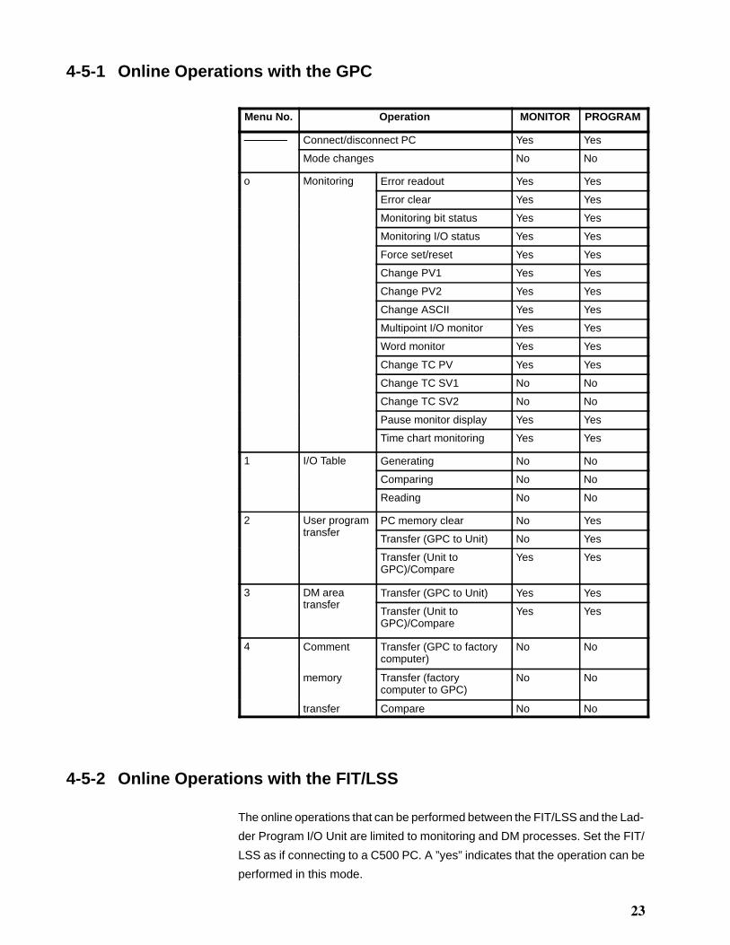
4-5-1 Online Operations with the GPC
Menu No. Operation MONITOR PROGRAM
Connect/disconnect PC Yes Yes
Mode changes No No
o Monitoring Error readout Yes Yesg
Error clear Yes Yes
Monitoring bit status Yes Yes
Monitoring I/O status Yes Yes
Force set/reset Yes Yes
Change PV1 Yes Yes
Change PV2 Yes Yes
Change ASCII Yes Yes
Multipoint I/O monitor Yes Yes
Word monitor Yes Yes
Change TC PV Yes Yes
Change TC SV1 No No
Change TC SV2 No No
Pause monitor display Yes Yes
Time chart monitoring Yes Yes
1 I/O Table Generating No No
Comparing No No
Reading No No
2 User programt f
PC memory clear No Yesgtransfer
Transfer (GPC to Unit) No Yes
Transfer (Unit toGPC)/Compare
Yes Yes
3 DM areat f
Transfer (GPC to Unit) Yes Yestransfer
Transfer (Unit toGPC)/Compare
Yes Yes
4 Comment Transfer (GPC to factorycomputer)
No No
memory Transfer (factorycomputer to GPC)
No No
transfer Compare No No
4-5-2 Online Operations with the FIT/LSS
The online operations that can be performed between the FIT/LSS and the Lad-
der Program I/O Unit are limited to monitoring and DM processes. Set the FIT/
LSS as if connecting to a C500 PC. A ”yes” indicates that the operation can be
performed in this mode.

�
Monitoring
Operation Application MONITOR PROGRAM
Monitor I/O status Yes Yes
Program transfer Ladder Program I/O Unit toFIT/LSS
Yes Yes
FIT/LSS to Ladder Program I/OUnit
Yes Yes
Compare Yes Yes
Ladder diagram (without comments) Yes Yes
Ladder diagram (with comments) Yes Yes
Online editing Line connection No Nog
I/O comments No No
Line comments No No
Scan time read No No
Data area clear No Yes
Search Yes Yes
I/O comments Yes Yes
Line comments Yes Yes
Memory display Yes Yes
I/O Monitor Operations
Operation MONITOR PROGRAM
Force Set/Reset Yes Yes
Basic Screen Function Keys
Function MONITOR PROGRAM
Release Yes Yes
Set value No No
Stop Yes Yes
Function Keys for Monitoring I/O
Function MONITOR mode PROGRAM mode
HEX:A Yes Yes
Release No No
Forced Release No No
Clear Yes Yes
Change Yes Yes
Stop Yes Yes
Note When checking TIM and TIMH(15) instructions with the ladder diagram monitoroperation while in MONITOR mode, the observed timing might be longer thanexpected.
��
��� �� �
���!��" �#������� ��"��!
/�� �!���� ��!��8� ��� �������" ���!���� �� ��� ��4: ��!"��� ��� ������� �6�!����� ! !"�: ��� �����!���� �6�!�����
����: ��� ��� '02 ������ ����� '� �"� ��!��8� ��� ��������� �� ��� ��������� ������
��� 2�������� �� (4 ��� 12 '/2( 1��� .� � � � � � � � � � � � � � � � � � � � � � � � � � � � � � � � � � � � �
�� �!�� /��� .� � � � � � � � � � � � � � � � � � � � � � � � � � � � � � � � � � � � � � � � � � � � � � � � � � � � � � � � � � � � � � �
��� '����!���� 56�!����� /��� 7� � � � � � � � � � � � � � � � � � � � � � � � � � � � � � � � � � � � � � � � � � � � � � � �
��� '02 (����� /��� �� � � � � � � � � � � � � � � � � � � � � � � � � � � � � � � � � � � � � � � � � � � � � � � � � � � � � � � �
����� ����" '02 /����� ��� � � � � � � � � � � � � � � � � � � � � � � � � � � � � � � � � � � � � � � � � � � � � � � �
���� ;�������� '���� ��� � � � � � � � � � � � � � � � � � � � � � � � � � � � � � � � � � � � � � � � � � � � � � � � �
�%
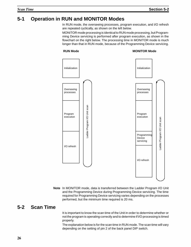
5-1 Operation in RUN and MONITOR ModesIn RUN mode, the overseeing processes, program execution, and I/O refreshare repeated cyclically, as shown on the left below.MONITOR mode processing is identical to RUN mode processing, but Program-ming Device servicing is performed after program execution, as shown in theflowchart on the right below. The processing time in MONITOR mode is muchlonger than that in RUN mode, because of the Programming Device servicing.
Initialization
Overseeingprocesses
Program
I/O refresh
Ladd
erP
rogr
amI/O
Uni
tsca
n
execution
RUN Mode
Initialization
Overseeingprocesses
Program
I/O refreshLa
dder
Pro
gram
I/OU
nits
canexecution
MONITOR Mode
ProgrammingDeviceservicing
Note In MONITOR mode, data is transferred between the Ladder Program I/O Unitand the Programming Device during Programming Device servicing. The timerequired for Programming Device servicing varies depending on the processesperformed, but the minimum time required is 20 ms.
5-2 Scan TimeIt is important to know the scan time of the Unit in order to determine whether ornot the program is operating correctly and to determine if I/O processing is timedproperly.The explanation below is for the scan time in RUN mode. The scan time will varydepending on the setting of pin 2 of the back panel DIP switch.
��� )��� Section 5-2

�$
Pin 2 ON (WRIT(87)/READ(88) Operation)Data is transferred to and from the PC using the I/O WRITE/READ(WRIT(87)/READ(88)) instructions.
Pin 2 OFF (Normal I/O Operation)Data is transferred to and from the PC through 2 words allocated for I/O.
Process Content Time requirements
Overseeing Watchdog timer set; indicators set, etc. 177 �s
Programexecution
Program executed. Total execution time for allinstructions varies with pro-gram size, the instructionsused, and execution condi-tions. Refer to InstructionExecution Times for details.
I/O refresh Pin 2 ON Pin 2 OFF Varies with the method ofdata transfer to/from the PC.
Input refreshWRIT(87)execution (seeNote 2 below)Clock read/storeREAD(88)execution (seeNote 2 below)Output refresh
Input refreshClock read/storeOutput refresh
Input refresh: 47.50 �sWRIT(87): 1.361 msClock read/store: 192.50 �sREAD(88): 753.75 �sOutput refresh: 35.00 �s
Scan time = Overseeing time + Program execution time + I/O refresh time
Note 1. The method of data transfer between the Unit and the PC is determined bythe setting of pin 2 of the back panel DIP switch.
The scan time is longer when pin 2 is ON, because of the time required toexecute WRIT(87) and READ(88), but these instructions allow a largeamount of data to be transferred all at once.
2. When WRIT(87) is executed during the I/O refresh, the data written from thePC is stored in DM 064 through DM 095 in the Unit.
When READ(88) is executed, the data stored in DM 096 through DM 127 inthe Unit is transferred to the PC.
3. The processing times given for the execution of WRIT(87) and READ(88)are the times required for the transfer of the maximum 32 words of data.
Long Scan Times
Scan time (ms) Possible adverse affects
10 or greater TIMH(15) inaccurate
100 or greater A watchdog timer error occurs, operation stops, and the Unitis automatically switched to PROGRAM mode.
Note If the scan time exceeds 100 ms, operation of the Unit is stopped and the Unit isautomatically switched to PROGRAM mode. It is necessary to recheck the pro-gram at this point.
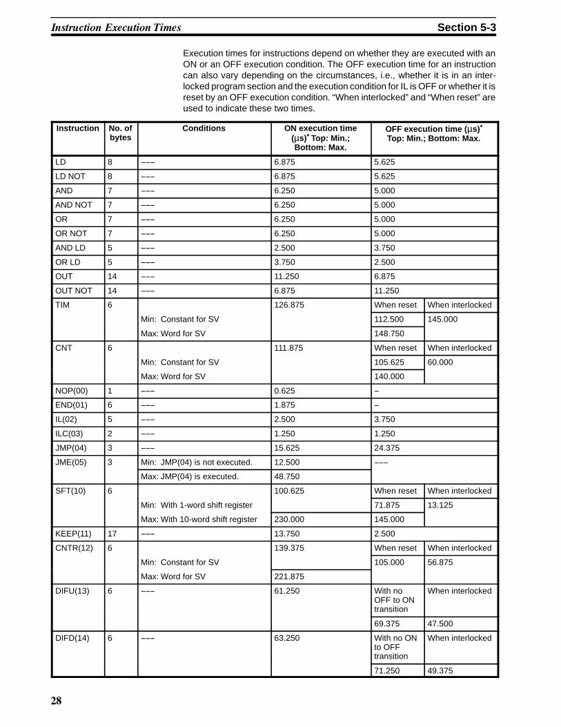
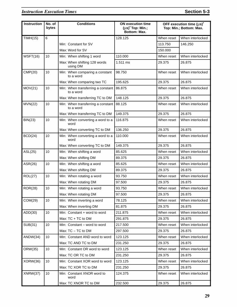
5-3 Instruction Execution TimesThis following table lists the execution times for all instructions that are availablefor the Ladder Program I/O Unit. The maximum and minimum execution timesand the conditions which cause them are given where relevant. When “word” isreferred to in the Conditions column, it implies the content of PC I/O bits, externalI/O bits, or work bits.
"��� ���� *+�� ��� )���� Section 5-3
�/
Execution times for instructions depend on whether they are executed with anON or an OFF execution condition. The OFF execution time for an instructioncan also vary depending on the circumstances, i.e., whether it is in an inter-locked program section and the execution condition for IL is OFF or whether it isreset by an OFF execution condition. “When interlocked” and “When reset” areused to indicate these two times.
Instruction No. ofbytes
Conditions ON execution time(µs)* Top: Min.;Bottom: Max.
OFF execution time ( µs)*
Top: Min.; Bottom: Max.
LD 8 ------ 6.875 5.625
LD NOT 8 ------ 6.875 5.625
AND 7 ------ 6.250 5.000
AND NOT 7 ------ 6.250 5.000
OR 7 ------ 6.250 5.000
OR NOT 7 ------ 6.250 5.000
AND LD 5 ------ 2.500 3.750
OR LD 5 ------ 3.750 2.500
OUT 14 ------ 11.250 6.875
OUT NOT 14 ------ 6.875 11.250
TIM 6 126.875 When reset When interlocked
Min: Constant for SV 112.500 145.000
Max: Word for SV 148.750
CNT 6 111.875 When reset When interlocked
Min: Constant for SV 105.625 60.000
Max: Word for SV 140.000
NOP(00) 1 ------ 0.625 --
END(01) 6 ------ 1.875 --
IL(02) 5 ------ 2.500 3.750
ILC(03) 2 ------ 1.250 1.250
JMP(04) 3 ------ 15.625 24.375
JME(05) 3 Min: JMP(04) is not executed. 12.500 ------
Max: JMP(04) is executed. 48.750
SFT(10) 6 100.625 When reset When interlocked
Min: With 1-word shift register 71.875 13.125
Max: With 10-word shift register 230.000 145.000
KEEP(11) 17 ------ 13.750 2.500
CNTR(12) 6 139.375 When reset When interlocked
Min: Constant for SV 105.000 56.875
Max: Word for SV 221.875
DIFU(13) 6 ------ 61.250 With noOFF to ONtransition
When interlocked
69.375 47.500
DIFD(14) 6 ------ 63.250 With no ONto OFFtransition
When interlocked
71.250 49.375
"��� ���� *+�� ��� )���� Section 5-3
�,
Instruction OFF execution time ( µs)*
Top: Min.; Bottom: Max.ON execution time
(µs)* Top: Min.;Bottom: Max.
ConditionsNo. ofbytes
TIMH(15) 6 128.125 When reset When interlocked
Min: Constant for SV 113.750 146.250
Max: Word for SV 150.000
WSFT(16) 10 Min: When shifting 1 word 110.000 When reset When interlocked
Max: When shifting 128 wordsusing DM
1.511 ms 29.375 26.875
CMP(20) 10 Min: When comparing a constantto a word
98.750 When reset When interlocked
Max: When comparing two TC 195.625 29.375 26.875
MOV(21) 10 Min: When transferring a constantto a word
86.875 When reset When interlocked
Max: When transferring TC to DM 148.125 29.375 26.875
MVN(22) 10 Min: When transferring a constantto a word
88.125 When reset When interlocked
Max: When transferring TC to DM 149.375 29.375 26.875
BIN(23) 10 Min: When converting a word to aword
116.875 When reset When interlocked
Max: When converting TC to DM 136.250 29.375 26.875
BCD(24) 10 Min: When converting a word to aword
110.000 When reset When interlocked
Max: When converting TC to DM 149.375 29.375 26.875
ASL(25) 10 Min: When shifting a word 85.625 When reset When interlocked
Max: When shifting DM 89.375 29.375 26.875
ASR(26) 10 Min: When shifting a word 85.625 When reset When interlocked
Max: When shifting DM 89.375 29.375 26.875
ROL(27) 10 Min: When rotating a word 93.750 When reset When interlocked
Max: When rotating DM 97.500 29.375 26.875
ROR(28) 10 Min: When rotating a word 93.750 When reset When interlocked
Max: When rotating DM 97.500 29.375 26.875
COM(29) 10 Min: When inverting a word 78.125 When reset When interlocked
Max: When inverting DM 81.875 29.375 26.875
ADD(30) 10 Min: Constant + word to word 211.875 When reset When interlocked
Max: TC + TC to DM 291.875 29.375 26.875
SUB(31) 10 Min: Constant -- word to word 217.500 When reset When interlocked
Max: TC -- TC to DM 297.500 29.375 26.875
ANDW(34) 10 Min: Constant AND word to word 123.125 When reset When interlocked
Max: TC AND TC to DM 231.250 29.375 26.875
ORW(35) 10 Min: Constant OR word to word 123.125 When reset When interlocked
Max: TC OR TC to DM 231.250 29.375 26.875
XORW(36) 10 Min: Constant XOR word to word 123.125 When reset When interlocked
Max: TC XOR TC to DM 231.250 29.375 26.875
XNRW(37) 10 Min: Constant XNOR word toword
124.375 When reset When interlocked
Max: TC XNOR TC to DM 232.500 29.375 26.875
"��� ���� *+�� ��� )���� Section 5-3
�0
Instruction OFF execution time ( µs)*
Top: Min.; Bottom: Max.ON execution time
(µs)* Top: Min.;Bottom: Max.
ConditionsNo. ofbytes
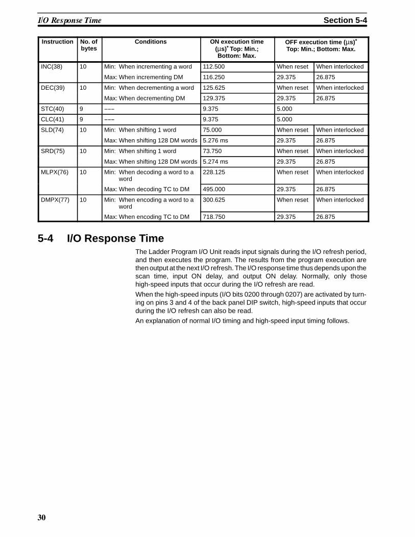
INC(38) 10 Min: When incrementing a word 112.500 When reset When interlocked
Max: When incrementing DM 116.250 29.375 26.875
DEC(39) 10 Min: When decrementing a word 125.625 When reset When interlocked
Max: When decrementing DM 129.375 29.375 26.875
STC(40) 9 ------ 9.375 5.000
CLC(41) 9 ------ 9.375 5.000
SLD(74) 10 Min: When shifting 1 word 75.000 When reset When interlocked
Max: When shifting 128 DM words 5.276 ms 29.375 26.875
SRD(75) 10 Min: When shifting 1 word 73.750 When reset When interlocked
Max: When shifting 128 DM words 5.274 ms 29.375 26.875
MLPX(76) 10 Min: When decoding a word to aword
228.125 When reset When interlocked
Max: When decoding TC to DM 495.000 29.375 26.875
DMPX(77) 10 Min: When encoding a word to aword
300.625 When reset When interlocked
Max: When encoding TC to DM 718.750 29.375 26.875
5-4 I/O Response TimeThe Ladder Program I/O Unit reads input signals during the I/O refresh period,and then executes the program. The results from the program execution arethen output at the next I/O refresh. The I/O response time thus depends upon thescan time, input ON delay, and output ON delay. Normally, only thosehigh-speed inputs that occur during the I/O refresh are read.
When the high-speed inputs (I/O bits 0200 through 0207) are activated by turn-ing on pins 3 and 4 of the back panel DIP switch, high-speed inputs that occurduring the I/O refresh can also be read.
An explanation of normal I/O timing and high-speed input timing follows.
",- #������ )��� Section 5-4
��
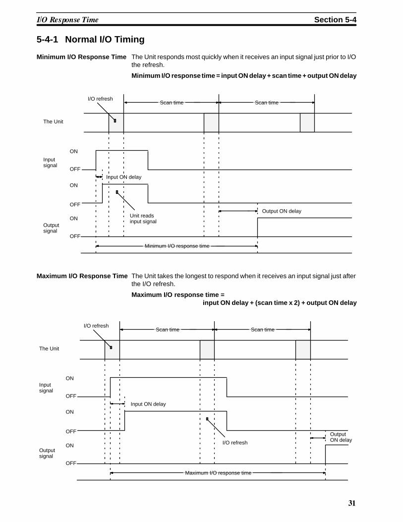
5-4-1 Normal I/O Timing
Minimum I/O Response Time The Unit responds most quickly when it receives an input signal just prior to I/Othe refresh.
Minimum I/O response time = input ON delay + scan time + output ON delay
Scan time Scan timeI/O refresh
The Unit
ON
Inputsignal
OFF
ON
OFF
ON
OFF
Outputsignal
Minimum I/O response time
Output ON delay
Input ON delay
Unit readsinput signal
Maximum I/O Response Time The Unit takes the longest to respond when it receives an input signal just afterthe I/O refresh.
Maximum I/O response time =input ON delay + (scan time x 2) + output ON delay
Scan time Scan timeI/O refresh
The Unit
ON
OFF
ON
OFF
ON
OFF
Maximum I/O response time
OutputON delay
Input ON delay
I/O refresh
Inputsignal
Outputsignal
",- #������ )��� Section 5-4

��
5-4-2 High-speed InputsHigh-speed inputs can be used by turning on pin 3 and/or pin 4 on the back panelDIP switch. Pin 3 enables high-speed inputs on IR 0200 through IR 0203; pin 4on IR 0204 through IR 0207. When high-speed inputs are enabled, any pulse of0.5 ms or longer will be acknowledged regardless of when it occurs, as shownbelow. The numbers in the following diagrams indicate processing as follows:
1, 2, 3... 1. When a pulse is received that is 0.5 ms or longer, the high-speed input bufferis turned ON. The ON status is maintained until the next refresh period re-gardless of whether or not the input remains ON.
2. When the next I/O refresh period is reached, the bit status is read from thehigh-speed input buffer to the input bit.
3. If the input is OFF during the I/O refresh period, the high-speed input bufferis turned OFF after status has been read. If the input is still ON, thehigh-speed input buffer remains ON at least until the next I/O refresh period.
4. Because the high-speed input buffer is reset if the input is OFF after readingstatus, the input bit is reset during the next I/O refresh period (unless the in-put has again come ON to activate the high-speed input buffer).
High-speed Inputs Between I/O Refresh Periods
Scan time Scan time Scan time
x
ba
(2)
(1)
(3)
(4)
I/O refresh
The Unit
ONInput bit
OFF
ON
OFF
ON
OFF
High-speedinput buffer
High-speedinput
a: Less than 0.5 msx: 0.5 msb: 0.5 ms or longer
High-speed Input Continuing after I/O Refresh Period
(3)
(1)
(2)(2)
(3)
(4)
I/O refresh
The Unit
ON
Input bitOFF
ON
OFF
ON
OFF
High-speedinput buffer
High-speedinput
x: 0.5 msb: 0.5 ms or longer
Scan time Scan time Scan time
x
b
",- #������ )��� Section 5-4

��
��� �� %
&���������� ��� ����'(��)�����!
/�� �!���� ���3��� ���������� ����!���� 8 4��� ����!���� ��� ����8"�������� ���� /�����!����� �� ���"�!� ��� ���
����� ��� 4��� � �"� ���3�����
$�� 5���� 1���� ��� /���8"�������� �$� � � � � � � � � � � � � � � � � � � � � � � � � � � � � � � � � � � � � � � � � �
$� 1��������!� �-� � � � � � � � � � � � � � � � � � � � � � � � � � � � � � � � � � � � � � � � � � � � � � � � � � � � � � � � � � � � �
�
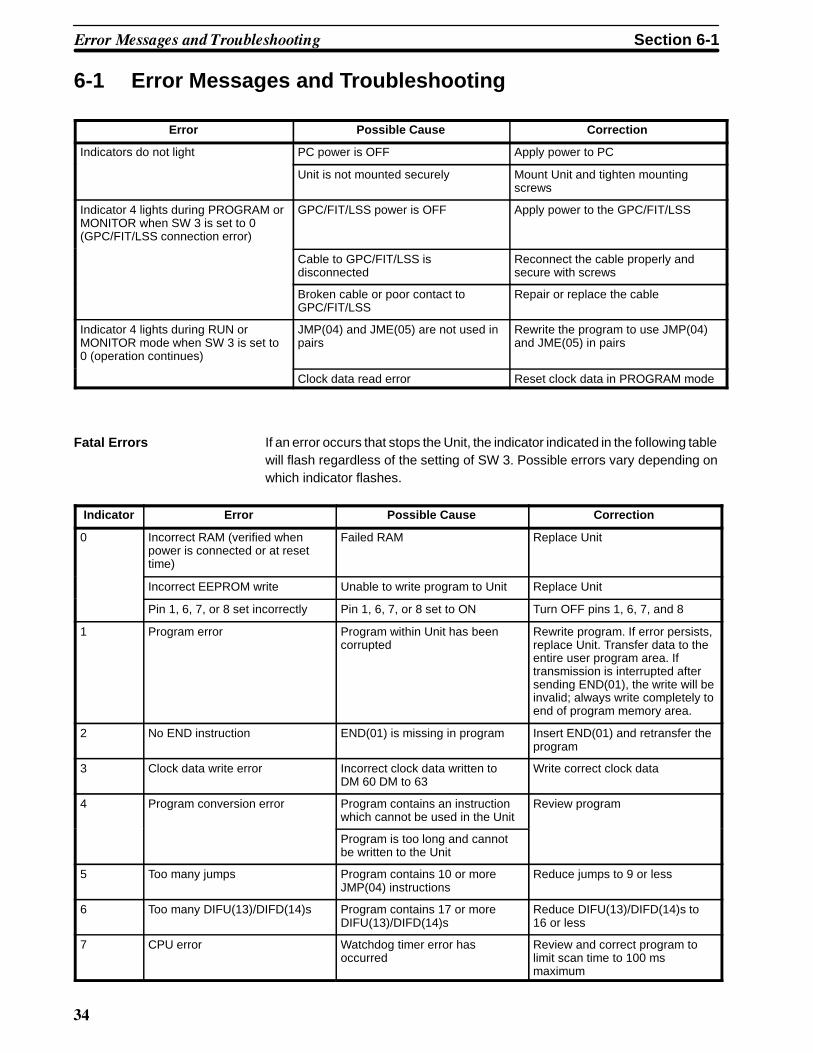
6-1 Error Messages and Troubleshooting
Error Possible Cause Correction
Indicators do not light PC power is OFF Apply power to PC
Unit is not mounted securely Mount Unit and tighten mountingscrews
Indicator 4 lights during PROGRAM orMONITOR when SW 3 is set to 0(GPC/FIT/LSS connection error)
GPC/FIT/LSS power is OFF Apply power to the GPC/FIT/LSS
Cable to GPC/FIT/LSS isdisconnected
Reconnect the cable properly andsecure with screws
Broken cable or poor contact toGPC/FIT/LSS
Repair or replace the cable
Indicator 4 lights during RUN orMONITOR mode when SW 3 is set to0 (operation continues)
JMP(04) and JME(05) are not used inpairs
Rewrite the program to use JMP(04)and JME(05) in pairs
Clock data read error Reset clock data in PROGRAM mode
Fatal Errors If an error occurs that stops the Unit, the indicator indicated in the following tablewill flash regardless of the setting of SW 3. Possible errors vary depending onwhich indicator flashes.
Indicator Error Possible Cause Correction
0 Incorrect RAM (verified whenpower is connected or at resettime)
Failed RAM Replace Unit
Incorrect EEPROM write Unable to write program to Unit Replace Unit
Pin 1, 6, 7, or 8 set incorrectly Pin 1, 6, 7, or 8 set to ON Turn OFF pins 1, 6, 7, and 8
1 Program error Program within Unit has beencorrupted
Rewrite program. If error persists,replace Unit. Transfer data to theentire user program area. Iftransmission is interrupted aftersending END(01), the write will beinvalid; always write completely toend of program memory area.
2 No END instruction END(01) is missing in program Insert END(01) and retransfer theprogram
3 Clock data write error Incorrect clock data written toDM 60 DM to 63
Write correct clock data
4 Program conversion error Program contains an instructionwhich cannot be used in the Unit
Review program
Program is too long and cannotbe written to the Unit
5 Too many jumps Program contains 10 or moreJMP(04) instructions
Reduce jumps to 9 or less
6 Too many DIFU(13)/DIFD(14)s Program contains 17 or moreDIFU(13)/DIFD(14)s
Reduce DIFU(13)/DIFD(14)s to16 or less
7 CPU error Watchdog timer error hasoccurred
Review and correct program tolimit scan time to 100 msmaximum
*���� (������� �� )�� .��������� Section 6-1
��
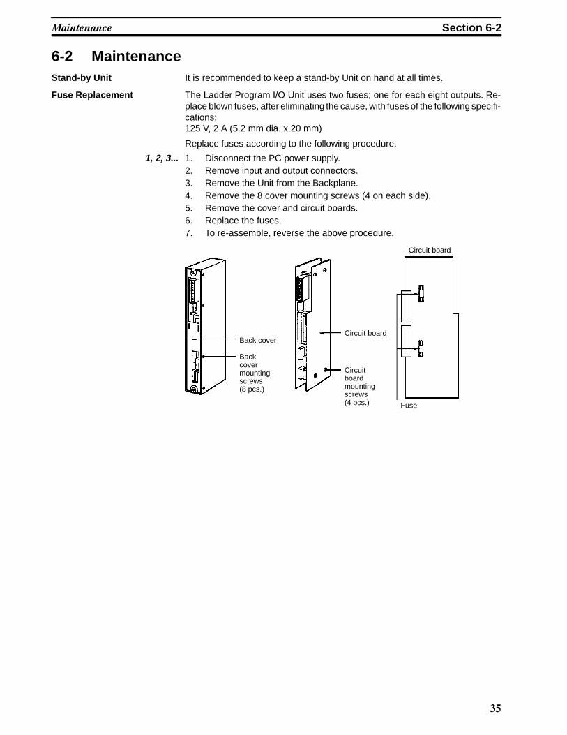
6-2 MaintenanceStand-by Unit It is recommended to keep a stand-by Unit on hand at all times.
Fuse Replacement The Ladder Program I/O Unit uses two fuses; one for each eight outputs. Re-place blown fuses, after eliminating the cause, with fuses of the following specifi-cations:125 V, 2 A (5.2 mm dia. x 20 mm)
Replace fuses according to the following procedure.
1, 2, 3... 1. Disconnect the PC power supply.2. Remove input and output connectors.3. Remove the Unit from the Backplane.4. Remove the 8 cover mounting screws (4 on each side).5. Remove the cover and circuit boards.6. Replace the fuses.7. To re-assemble, reverse the above procedure.
Back cover
Backcovermountingscrews(8 pcs.)
Circuit board
Circuitboardmountingscrews(4 pcs.) Fuse
Circuit board
(������� Section 6-2

�$
Appendix AStandard Models
Product Name Model No.
Ladder Program I/O Unit C500-LDP01-V1
GPC Main unit 3G2C5-GPC03-E/3G2C5-GPC04-E
System Memory Cassette C500-MP303-EV2
FIT FIT10-SET11-E
LSS 3 1/2” FD 720 KB (4 floppy disks) C500-SF312-EV2
5 1/4” FD 360 KB (8 floppy disks) C500-SF711-EV2
�,
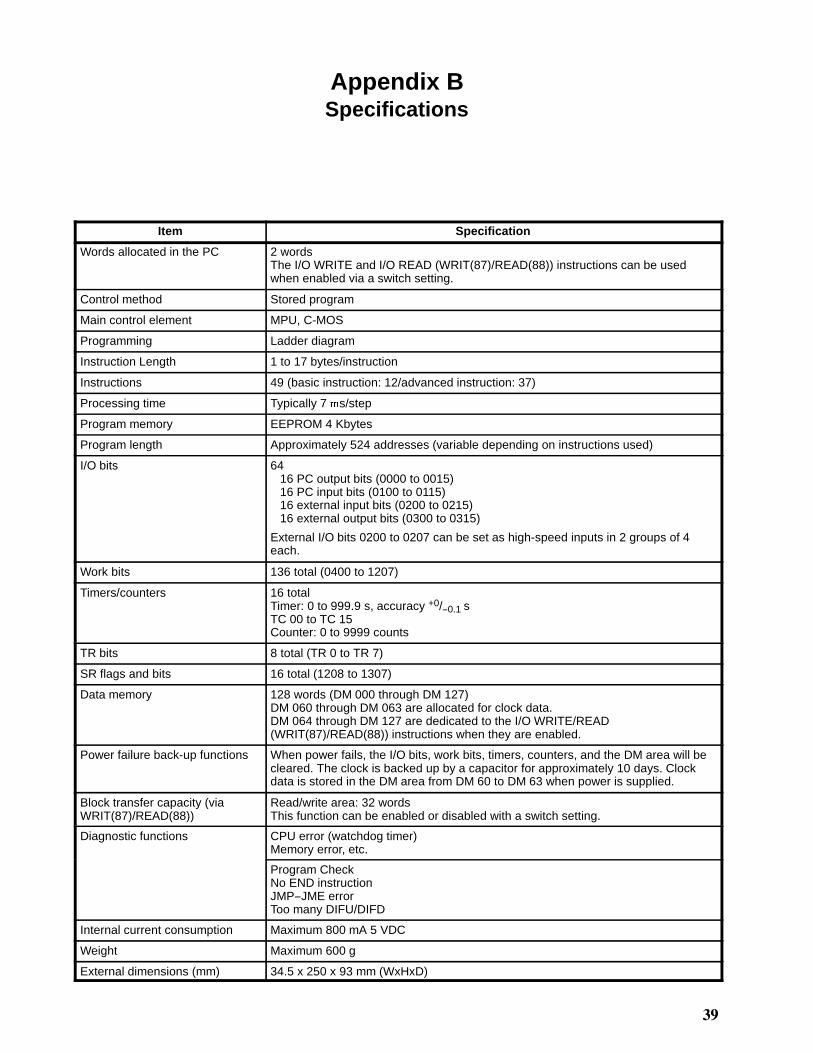
Appendix BSpecifications
Item Specification
Words allocated in the PC 2 wordsThe I/O WRITE and I/O READ (WRIT(87)/READ(88)) instructions can be usedwhen enabled via a switch setting.
Control method Stored program
Main control element MPU, C-MOS
Programming Ladder diagram
Instruction Length 1 to 17 bytes/instruction
Instructions 49 (basic instruction: 12/advanced instruction: 37)
Processing time Typically 7 �s/step
Program memory EEPROM 4 Kbytes
Program length Approximately 524 addresses (variable depending on instructions used)
I/O bits 6416 PC output bits (0000 to 0015)16 PC input bits (0100 to 0115)16 external input bits (0200 to 0215)16 external output bits (0300 to 0315)
External I/O bits 0200 to 0207 can be set as high-speed inputs in 2 groups of 4each.
Work bits 136 total (0400 to 1207)
Timers/counters 16 totalTimer: 0 to 999.9 s, accuracy +0/--0.1 sTC 00 to TC 15Counter: 0 to 9999 counts
TR bits 8 total (TR 0 to TR 7)
SR flags and bits 16 total (1208 to 1307)
Data memory 128 words (DM 000 through DM 127)DM 060 through DM 063 are allocated for clock data.DM 064 through DM 127 are dedicated to the I/O WRITE/READ(WRIT(87)/READ(88)) instructions when they are enabled.
Power failure back-up functions When power fails, the I/O bits, work bits, timers, counters, and the DM area will becleared. The clock is backed up by a capacitor for approximately 10 days. Clockdata is stored in the DM area from DM 60 to DM 63 when power is supplied.
Block transfer capacity (viaWRIT(87)/READ(88))
Read/write area: 32 wordsThis function can be enabled or disabled with a switch setting.
Diagnostic functions CPU error (watchdog timer)Memory error, etc.
Program CheckNo END instructionJMP--JME errorToo many DIFU/DIFD
Internal current consumption Maximum 800 mA 5 VDC
Weight Maximum 600 g
External dimensions (mm) 34.5 x 250 x 93 mm (WxHxD)
Appendix B������������
0
External Input/Output Specifications
DC inputs
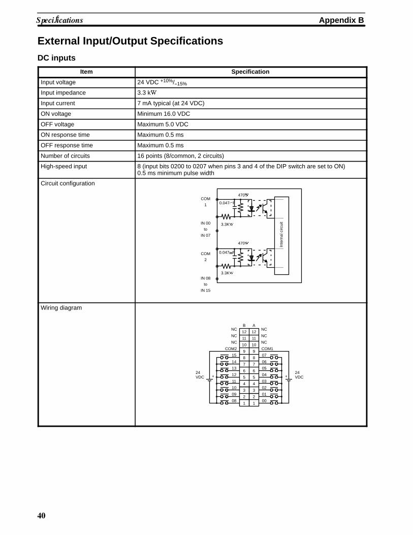
Item Specification
Input voltage 24 VDC +10%/--15%
Input impedance 3.3 k"
Input current 7 mA typical (at 24 VDC)
ON voltage Minimum 16.0 VDC
OFF voltage Maximum 5.0 VDC
ON response time Maximum 0.5 ms
OFF response time Maximum 0.5 ms
Number of circuits 16 points (8/common, 2 circuits)
High-speed input 8 (input bits 0200 to 0207 when pins 3 and 4 of the DIP switch are set to ON)0.5 ms minimum pulse width
Circuit configuration
0.047�F
0.047�FCOM
1
IN 00
to
IN 07
COM
2
IN 08
to
IN 15
470�
3.3K�
470�
3.3K�
Inte
rnal
circ
uit
Wiring diagram
0614
1
2
3
4
5
6
7
8
9
10
11
12
B
08
COM2
NC
NC
NC
1
2
3
4
5
6
7
8
9
10
11
12
A
00
COM1
NC
NC
NC
09
10
11
12
13
15
01
02
03
04
05
07
++24VDC
24VDC
Appendix B������������
�
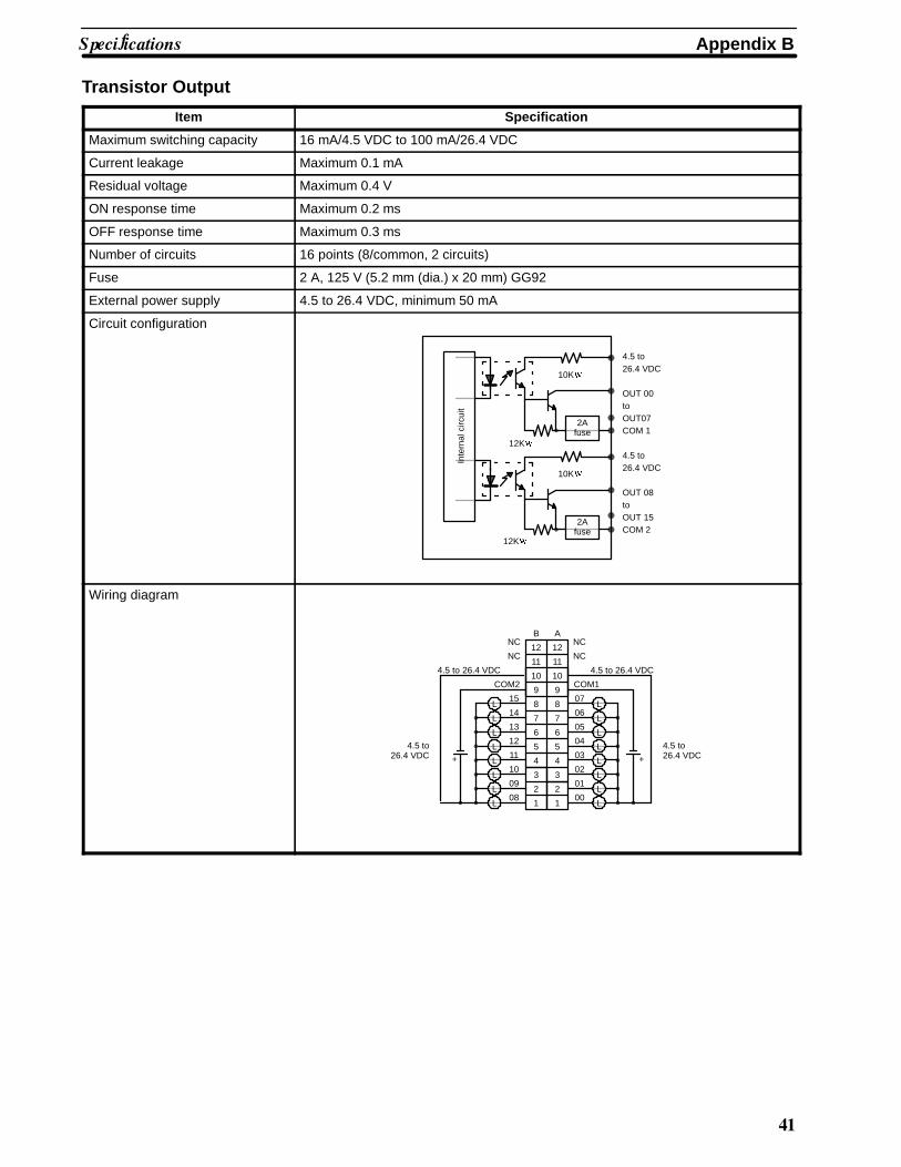
Transistor Output
Item Specification
Maximum switching capacity 16 mA/4.5 VDC to 100 mA/26.4 VDC
Current leakage Maximum 0.1 mA
Residual voltage Maximum 0.4 V
ON response time Maximum 0.2 ms
OFF response time Maximum 0.3 ms
Number of circuits 16 points (8/common, 2 circuits)
Fuse 2 A, 125 V (5.2 mm (dia.) x 20 mm) GG92
External power supply 4.5 to 26.4 VDC, minimum 50 mA
Circuit configuration
10K�
12K�
2Afuse
Inte
rnal
circ
uit
4.5 to26.4 VDC
OUT 00toOUT07COM 1
4.5 to26.4 VDC
OUT 08toOUT 15COM 2
10K�
12K�
2Afuse
Wiring diagram
0614
1
2
3
4
5
6
7
8
9
10
11
12
B
08
COM2
NC
NC
1
2
3
4
5
6
7
8
9
10
11
12
A
00
COM1
NC
NC
09
10
11
12
13
15
01
02
03
04
05
07
++
4.5 to26.4 VDC
4.5 to 26.4 VDC4.5 to 26.4 VDC
4.5 to26.4 VDC
L
L
L
L
L
L
L
LL
L
L
L
L
L
L
L
Appendix B������������
�
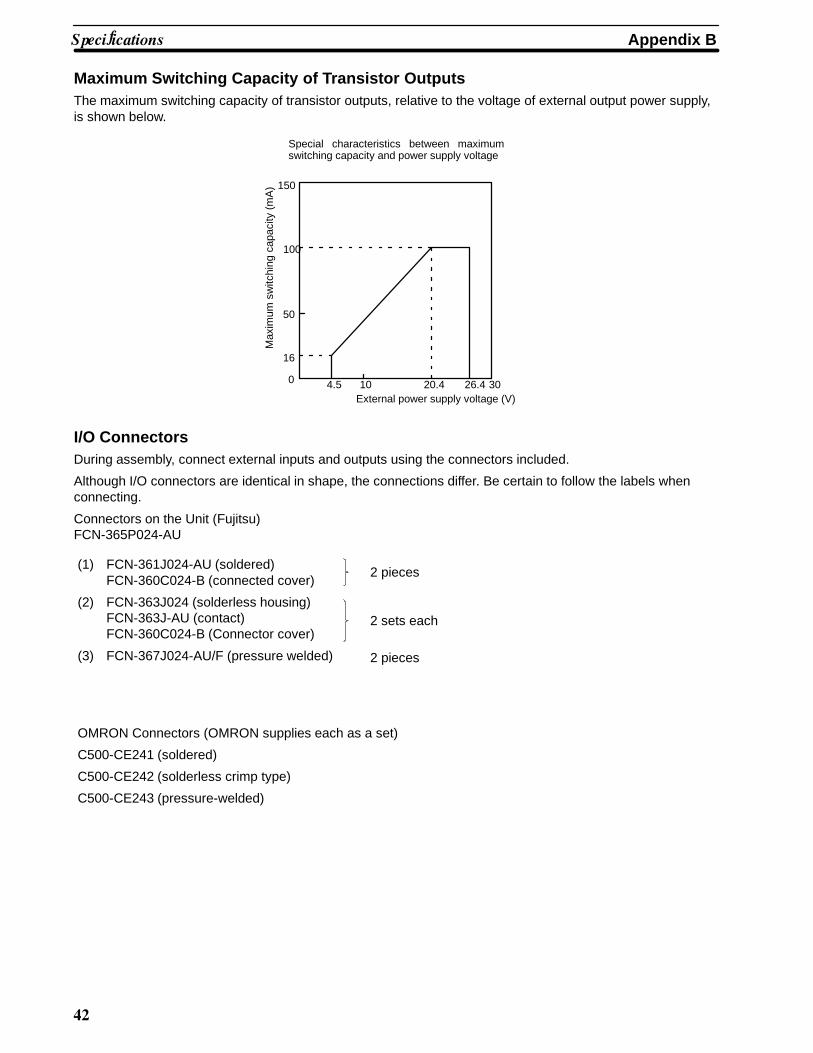
Maximum Switching Capacity of Transistor OutputsThe maximum switching capacity of transistor outputs, relative to the voltage of external output power supply,is shown below.
150
100
50
16
0 4.5 10 20.4 26.4 30External power supply voltage (V)
Special characteristics between maximumswitching capacity and power supply voltage
Max
imum
switc
hing
capa
city
(mA
)
I/O ConnectorsDuring assembly, connect external inputs and outputs using the connectors included.
Although I/O connectors are identical in shape, the connections differ. Be certain to follow the labels whenconnecting.
Connectors on the Unit (Fujitsu)FCN-365P024-AU
(1) FCN-361J024-AU (soldered)FCN-360C024-B (connected cover)
(2) FCN-363J024 (solderless housing)FCN-363J-AU (contact)FCN-360C024-B (Connector cover)
(3) FCN-367J024-AU/F (pressure welded)
OMRON Connectors (OMRON supplies each as a set)
C500-CE241 (soldered)
C500-CE242 (solderless crimp type)
C500-CE243 (pressure-welded)
2 pieces
2 sets each
2 pieces
�
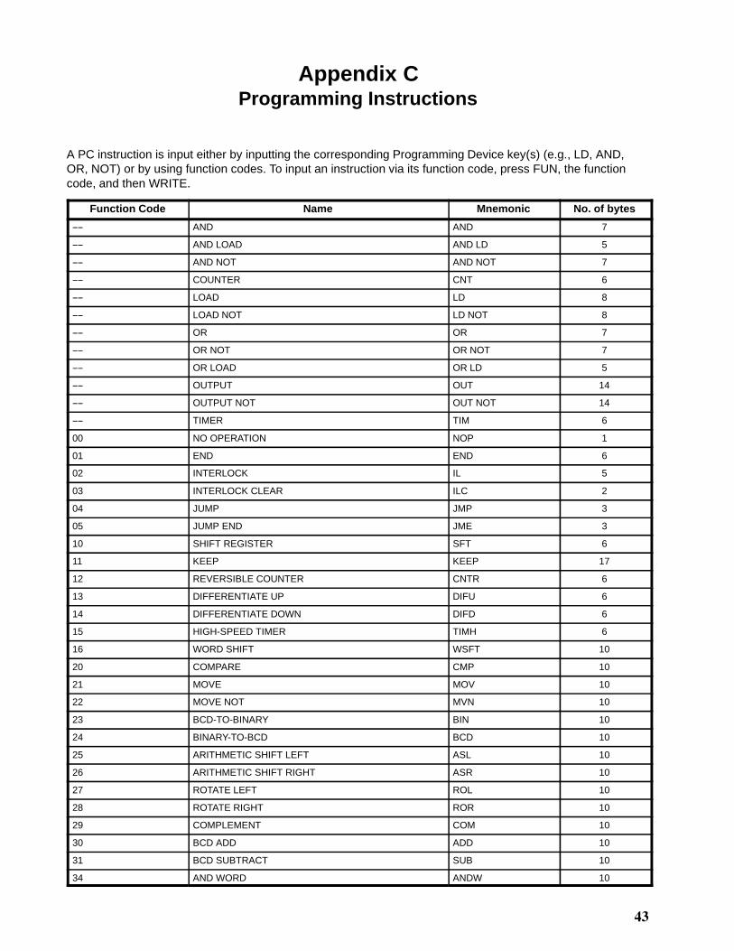
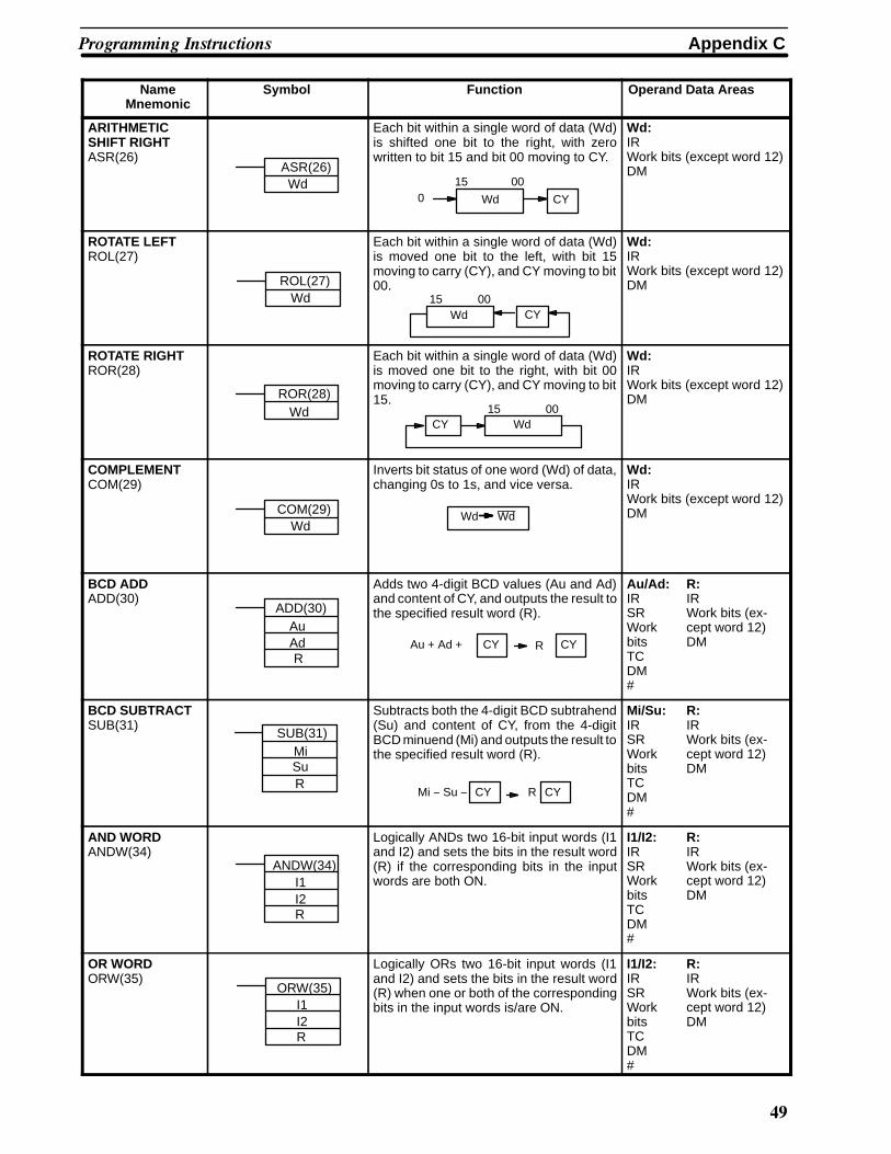
Appendix CProgramming Instructions
A PC instruction is input either by inputting the corresponding Programming Device key(s) (e.g., LD, AND,OR, NOT) or by using function codes. To input an instruction via its function code, press FUN, the functioncode, and then WRITE.
Function Code Name Mnemonic No. of bytes
---- AND AND 7
---- AND LOAD AND LD 5
---- AND NOT AND NOT 7
---- COUNTER CNT 6
---- LOAD LD 8
---- LOAD NOT LD NOT 8
---- OR OR 7
---- OR NOT OR NOT 7
---- OR LOAD OR LD 5
---- OUTPUT OUT 14
---- OUTPUT NOT OUT NOT 14
---- TIMER TIM 6
00 NO OPERATION NOP 1
01 END END 6
02 INTERLOCK IL 5
03 INTERLOCK CLEAR ILC 2
04 JUMP JMP 3
05 JUMP END JME 3
10 SHIFT REGISTER SFT 6
11 KEEP KEEP 17
12 REVERSIBLE COUNTER CNTR 6
13 DIFFERENTIATE UP DIFU 6
14 DIFFERENTIATE DOWN DIFD 6
15 HIGH-SPEED TIMER TIMH 6
16 WORD SHIFT WSFT 10
20 COMPARE CMP 10
21 MOVE MOV 10
22 MOVE NOT MVN 10
23 BCD-TO-BINARY BIN 10
24 BINARY-TO-BCD BCD 10
25 ARITHMETIC SHIFT LEFT ASL 10
26 ARITHMETIC SHIFT RIGHT ASR 10
27 ROTATE LEFT ROL 10
28 ROTATE RIGHT ROR 10
29 COMPLEMENT COM 10
30 BCD ADD ADD 10
31 BCD SUBTRACT SUB 10
34 AND WORD ANDW 10
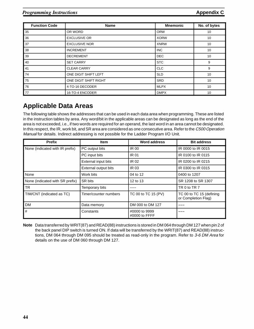
Appendix C���������� "��� �����
Function Code No. of bytesMnemonicName
35 OR WORD ORW 10
36 EXCLUSIVE OR XORW 10
37 EXCLUSIVE NOR XNRW 10
38 INCREMENT INC 10
39 DECREMENT DEC 10
40 SET CARRY STC 9
41 CLEAR CARRY CLC 9
74 ONE DIGIT SHIFT LEFT SLD 10
75 ONE DIGIT SHIFT RIGHT SRD 10
76 4-TO-16 DECODER MLPX 10
77 16-TO-4 ENCODER DMPX 10
Applicable Data AreasThe following table shows the addresses that can be used in each data area when programming. These are listedin the instruction tables by area. Any word/bit in the applicable areas can be designated as long as the end of thearea is not exceeded, i.e., if two words are required for an operand, the last word in an area cannot be designated.In this respect, the IR, work bit, and SR area are considered as one consecutive area. Refer to the C500 OperationManual for details. Indirect addressing is not possible for the Ladder Program I/O Unit.
Prefix Item Word address Bit address
None (indicated with IR prefix) PC output bits IR 00 IR 0000 to IR 0015
PC input bits IR 01 IR 0100 to IR 0115
External input bits IR 02 IR 0200 to IR 0215
External output bits IR 03 IR 0300 to IR 0315
None Work bits 04 to 12 0400 to 1207
None (indicated with SR prefix) SR bits 12 to 13 SR 1208 to SR 1307
TR Temporary bits ------ TR 0 to TR 7
TIM/CNT (indicated as TC) Timer/counter numbers TC 00 to TC 15 (PV) TC 00 to TC 15 (definingor Completion Flag)
DM Data memory DM 000 to DM 127 ------
# Constants #0000 to 9999#0000 to FFFF
------
Note Data transferred by WRIT(87) and READ(88) instructions is stored in DM 064 through DM 127 when pin 2 ofthe back panel DIP switch is turned ON. If data will be transferred by the WRIT(87) and READ(88) instruc-tions, DM 064 through DM 095 should be treated as read-only in the program. Refer to 3-6 DM Area fordetails on the use of DM 060 through DM 127.
Appendix C���������� "��� �����
�
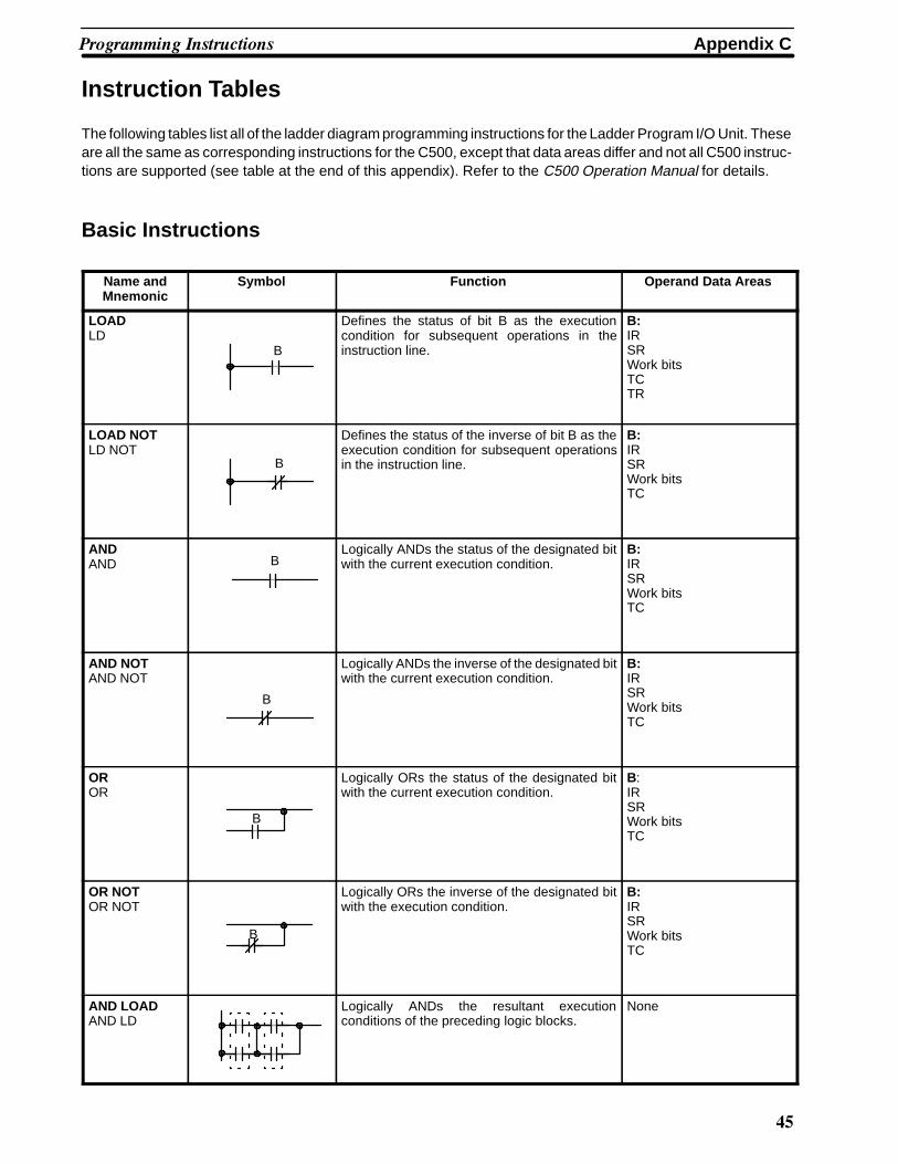
Instruction Tables
The following tables list all of the ladder diagram programming instructions for the Ladder Program I/O Unit. Theseare all the same as corresponding instructions for the C500, except that data areas differ and not all C500 instruc-tions are supported (see table at the end of this appendix). Refer to the C500 Operation Manual for details.
Basic Instructions
Name andMnemonic
Symbol Function Operand Data Areas
LOADLD
B
Defines the status of bit B as the executioncondition for subsequent operations in theinstruction line.
B:IRSRWork bitsTCTR
LOAD NOTLD NOT
B
Defines the status of the inverse of bit B as theexecution condition for subsequent operationsin the instruction line.
B:IRSRWork bitsTC
ANDAND B
Logically ANDs the status of the designated bitwith the current execution condition.
B:IRSRWork bitsTC
AND NOTAND NOT
B
Logically ANDs the inverse of the designated bitwith the current execution condition.
B:IRSRWork bitsTC
OROR
B
Logically ORs the status of the designated bitwith the current execution condition.
B:IRSRWork bitsTC
OR NOTOR NOT
B
Logically ORs the inverse of the designated bitwith the execution condition.
B:IRSRWork bitsTC
AND LOADAND LD
Logically ANDs the resultant executionconditions of the preceding logic blocks.
None
Appendix C���������� "��� �����
%
Name andMnemonic
Operand Data AreasFunctionSymbol
OR LOADOR LD
Logically ORs the resultant execution conditionsof the preceding logic blocks.
None
OUTPUTOUT
B
Turns ON B for an ON execution condition; turnsOFF B for an OFF execution condition.
B:IR (except IR 00 and IR 02)Work bitsTR
OUTPUT NOTOUT NOT
B
Turns OFF B for an ON execution condition;turns ON B for an OFF execution condition.
B:IR (except IR 00 and IR 02)Work bits
COUNTERCNT
CNT N
SV
CP
R
A decrementing counter. SV: 0 to 9999; CP:count pulse; R: reset input. The TC bit is enteredas a constant.
N:TC
SV:IRSRWork bits#
TIMERTIM
TIM N
SV
ON-delay (decrementing) timer operation. Setvalue: 000.0 to 999.9 s. The same TC bit cannotbe assigned to more than one timer/counter. TheTC bit is entered as a constant.
N:TC
SV:IRSRWork bits#
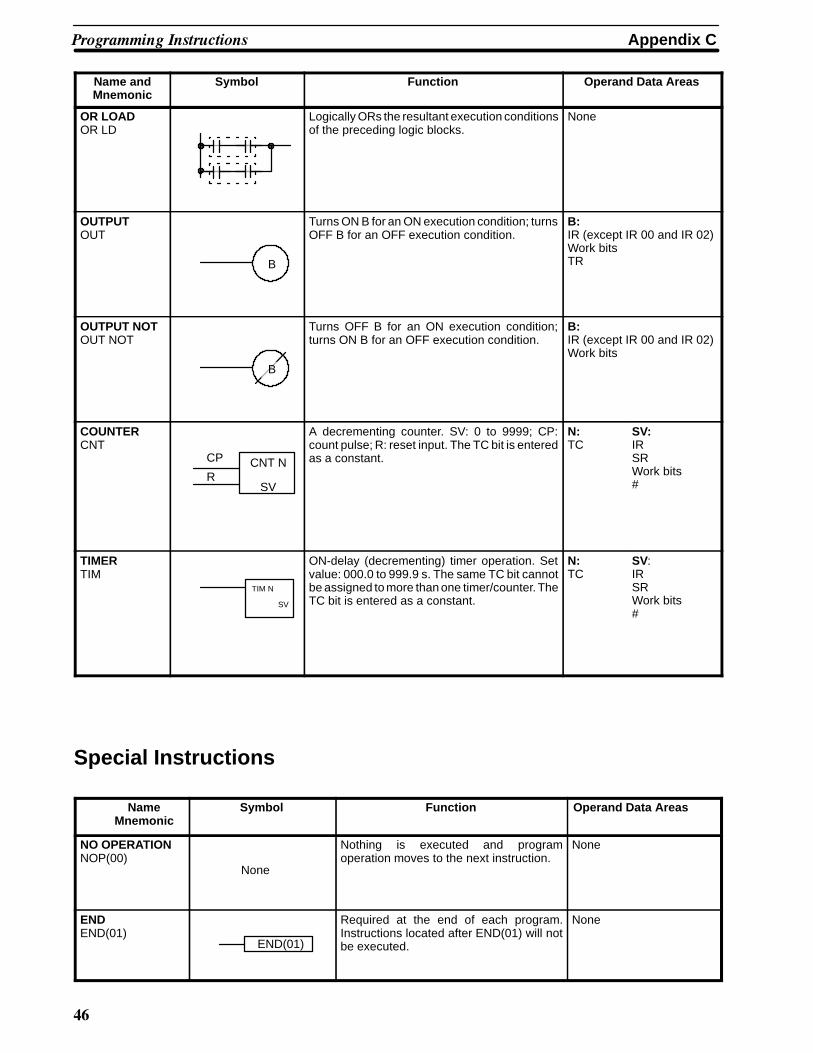
Special Instructions
NameMnemonic
Symbol Function Operand Data Areas
NO OPERATIONNOP(00)
None
Nothing is executed and programoperation moves to the next instruction.
None
ENDEND(01)
END(01)
Required at the end of each program.Instructions located after END(01) will notbe executed.
None
Appendix C���������� "��� �����
$
NameMnemonic
Operand Data AreasFunctionSymbol
INTERLOCKIL(02)INTERLOCKCLEARILC(03)
IL(02)
ILC(03)
If an interlock condition is OFF, all outputsand all timer PVs between the currentIL(02) and the next ILC(03) are turned OFFor reset, respectively. Other instructionsare treated as NOP. Counter PVs aremaintained. If the execution condition isON, execution continues normally.
None
JUMPJMP(04)JUMP ENDJME(05)
JMP(04)
JME(05)
When the execution condition for theJMP(04) instruction is ON, all instructionsbetween JMP(04) and the next JME(05)are ignored or treated as NOP(00)
None
SHIFT REGISTERSFT(10) I
P
R
SFT(10)StE
Creates a bit shift register for data from thestarting word (St) through to the endingword (E). I: input bit; P: shift pulse; R: resetinput. St must be less than or equal to E. Stand E must be in the same data area.
E St15 1500
IN00
St/E:IR (except IR00 and IR02)Work bits (except word 12)
KEEPKEEP(11)
S
KEEP(11)
BR
Defines a bit (B) as a latch, controlled bythe set (S) and reset (R) inputs.
B:IR (except IR00 and IR02)Work bits
REVERSIBLECOUNTERCNTR (12)
II
DI
RN
SV
CNTR(12)
Increases or decreases the PV by onewhenever the increment input (II) ordecrement input (DI) signals, respectively,go from OFF to ON. SV: 0 to 9999; R: resetinput. Each TC bit can be used for onetimer/counter only. The TC bit is entered asa constant.
N:TC
SV:IRSRWork bits#
DIFFERENTIATEUPDIFU(13)DIFFERENTIATEDOWNDIFD(14)
DIFU(13)
DIFD(14)
B
B
DIFU(13) turns ON the designated bit (B)for one scan on reception of the leading(rising) edge of the input signal; DIFD(14)turns ON the bit for one scan on receptionof the trailing (falling) edge. A maximum of16 DIFFERENTIATE UP/DOWN instruc-tions can be used
B:IR (except IR00 and IR02)Work bits
HIGH-SPEEDTIMERTIMH(15) TIMH(15) N
SV
A high-speed, ON-delay (decrementing)timer. SV: 00.02 to 99.99 s. Each TC bit canbe assigned to only one timer or counter.The TC bit is entered as a constant.
N:TC
SV:IRSRWork bits#
WORD SHIFTWSFT(16)
WSFT(16)
ESt
The data in the words from the startingword (St) through to the ending word (E), isshifted left in word units, writing all zerosinto the starting word. St must be less thanor equal to E, and St and E must be in thesame data area.
St/E:IRWork bits (except word 12)

Appendix C���������� "��� �����
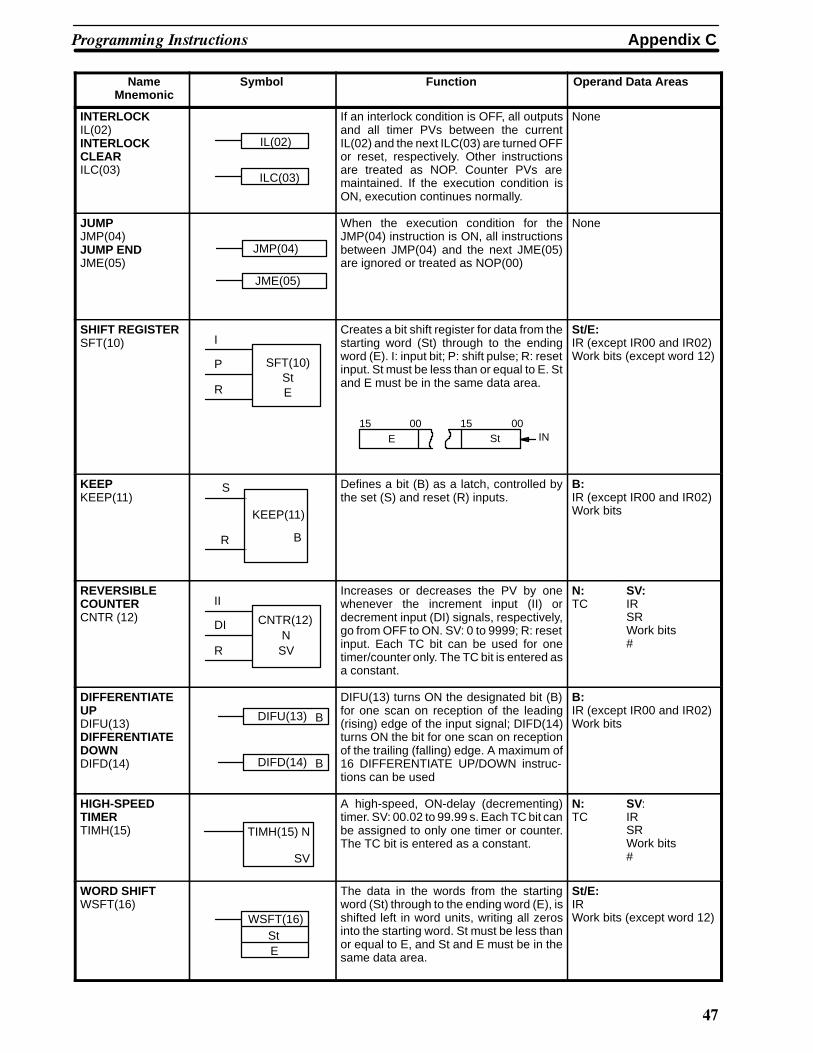
/
NameMnemonic
Operand Data AreasFunctionSymbol
COMPARECMP(20)
CMP(20)Cp1Cp2
Compares the data in two 4-digithexadecimal words (Cp1 and Cp2) andoutputs result to the GR, EQ, or LE Flags.
Cp1/Cp2:IRSRWork bitsTCDM#
MOVEMOV(21)
MOV(21)SD
Transfers data from source word, (S) todestination word (D).
S:IRSRWorkbitsTCDM#
D:IRWork bits (ex-cept word 12)DM
MOVE NOTMVN(22)
MVN(22)SD
Transfers the inverse of the data in thesource word (S) to destination word (D).
S:IRSRWorkbitsTCDM#
D:IRWork bits (ex-cept word 12)DM
BCD TO BINARYBIN(23)
BIN(23)SR
Converts 4-digit, BCD data in source word(S) into 16-bit binary data, and outputsconverted data to result word (R).
S
x100
x101
x102
x103
x160
x161
x162
x163
(BCD) (BIN)R
S:IRSRWorkbitsTCDM
R:IRWork bits (ex-cept word 12)DM
BINARY TO BCDBCD(24)
BCD(24)SR
Converts binary data in source word (S)into BCD, and outputs converted data toresult word (R).
x160
x161
x162
x163
x101
x102
x103
S R(BIN) (BCD)
x100
S:IRSRWorkbitsDM
R:IRWork bits (ex-cept word 12)DM
ARITHMETICSHIFT LEFTASL(25)
ASL(25)Wd
Each bit within a single word of data (Wd)is shifted one bit to the left, with zero writtento bit 00 and bit 15 moving to CY.
Wd
15 00
CY 0
Wd:IRWork bits (except word 12)DM
Appendix C���������� "��� �����
,
NameMnemonic
Operand Data AreasFunctionSymbol
ARITHMETICSHIFT RIGHTASR(26)
ASR(26)Wd
Each bit within a single word of data (Wd)is shifted one bit to the right, with zerowritten to bit 15 and bit 00 moving to CY.
0 Wd CY
15 00
Wd:IRWork bits (except word 12)DM
ROTATE LEFTROL(27)
ROL(27)Wd
Each bit within a single word of data (Wd)is moved one bit to the left, with bit 15moving to carry (CY), and CY moving to bit00.
15 00CYWd
Wd:IRWork bits (except word 12)DM
ROTATE RIGHTROR(28)
ROR(28)Wd 15 00
CY Wd
Each bit within a single word of data (Wd)is moved one bit to the right, with bit 00moving to carry (CY), and CY moving to bit15.
Wd:IRWork bits (except word 12)DM
COMPLEMENTCOM(29)
COM(29)Wd
Inverts bit status of one word (Wd) of data,changing 0s to 1s, and vice versa.
Wd Wd
Wd:IRWork bits (except word 12)DM
BCD ADDADD(30)
ADD(30)AuAdR
CY CY
Adds two 4-digit BCD values (Au and Ad)and content of CY, and outputs the result tothe specified result word (R).
Au + Ad + R
Au/Ad:IRSRWorkbitsTCDM#
R:IRWork bits (ex-cept word 12)DM
BCD SUBTRACTSUB(31)
SUB(31)MiSuR
Subtracts both the 4-digit BCD subtrahend(Su) and content of CY, from the 4-digitBCD minuend (Mi) and outputs the result tothe specified result word (R).
CYMi -- Su -- R CY
Mi/Su:IRSRWorkbitsTCDM#
R:IRWork bits (ex-cept word 12)DM
AND WORDANDW(34)
ANDW(34)I1I2R
Logically ANDs two 16-bit input words (I1and I2) and sets the bits in the result word(R) if the corresponding bits in the inputwords are both ON.
I1/I2:IRSRWorkbitsTCDM#
R:IRWork bits (ex-cept word 12)DM
OR WORDORW(35)
ORW(35)I1I2R
Logically ORs two 16-bit input words (I1and I2) and sets the bits in the result word(R) when one or both of the correspondingbits in the input words is/are ON.
I1/I2:IRSRWorkbitsTCDM#
R:IRWork bits (ex-cept word 12)DM
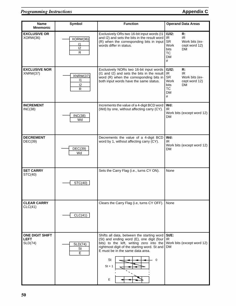
Appendix C���������� "��� �����
�0
NameMnemonic
Operand Data AreasFunctionSymbol
EXCLUSIVE ORXORW(36) XORW(36)
I1I2R
Exclusively ORs two 16-bit input words (I1and I2) and sets the bits in the result word(R) when the corresponding bits in inputwords differ in status.
I1/I2:IRSRWorkbitsTCDM#
R:IRWork bits (ex-cept word 12)DM
EXCLUSIVE NORXNRW(37)
I1I2R
XNRW(37)
Exclusively NORs two 16-bit input words(I1 and I2) and sets the bits in the resultword (R) when the corresponding bits inboth input words have the same status.
I1/I2:IRSRWorkbitsTCDM#
R:IRWork bits (ex-cept word 12)DM
INCREMENTINC(38)
INC(38)Wd
Increments the value of a 4-digit BCD word(Wd) by one, without affecting carry (CY).
Wd:IRWork bits (except word 12)DM
DECREMENTDEC(39)
DEC(39)Wd
Decrements the value of a 4-digit BCDword by 1, without affecting carry (CY).
Wd:IRWork bits (except word 12)DM
SET CARRYSTC(40)
STC(40)
Sets the Carry Flag (i.e., turns CY ON). None
CLEAR CARRYCLC(41)
CLC(41)
Clears the Carry Flag (i.e, turns CY OFF). None
ONE DIGIT SHIFTLEFTSLD(74) SLD(74)
StE
Shifts all data, between the starting word(St) and ending word (E), one digit (fourbits) to the left, writing zero into therightmost digit of the starting word. St andE must be in the same data area.
E
St
St + 1
0
St/E:IRWork bits (except word 12)DM

Appendix C���������� "��� �����
��
NameMnemonic
Operand Data AreasFunctionSymbol
ONE DIGIT SHIFTRIGHTSRD(75)
SRD(75)ESt
0 St
Shifts all data, between starting word (St)and ending word (E), one digit (four bits) tothe right, writing zero into the leftmost digitof the ending word. St and E must be in thesame data area.
E
E -- 1
St/E:IRWork bits (except word 12)DM
4-TO-16DECODERMLPX(76) MLPX(76)
SDiR
Converts up to four hexadecimal digits inthe source word (S), into decimal valuesfrom 0 to 15, and turns ON thecorresponding bit(s) in the result word(s)(R). There is one result word for eachconverted digit. Digits to be converted aredesignated by Di. (The rightmost digitspecifies the first digit. The next digit to theleft gives the number of digits to beconverted minus 1. The two leftmost digitsare not used.)
S 0 to F
R
0015
S:IRSRWorkbitsTCDM
Di:IRWorkbits (ex-ceptword12)TCDM#
R:IRWorkbits(ex-ceptword12)DM
16-TO-4ENCODERDMPX(77) DMPX(77)
SRDi
Determines the position of the leftmost ONbit in the source word(s) (starting word: S)and turns ON the corresponding bit(s) inthe specified digit of the result word (R).One digit is used for each source word.Digits to receive the converted values aredesignated by Di. (The rightmost digitspecifies the first digit. The next digit to leftgives the number of words to be convertedminus 1. The two leftmost digits are notused.)
S
15 00
0 to FR
S:IRSRWorkbitsTCDM
R:IRWorkbits (ex-ceptword12)DM
Di:IRWorkbits(ex-ceptword12)TCDM#
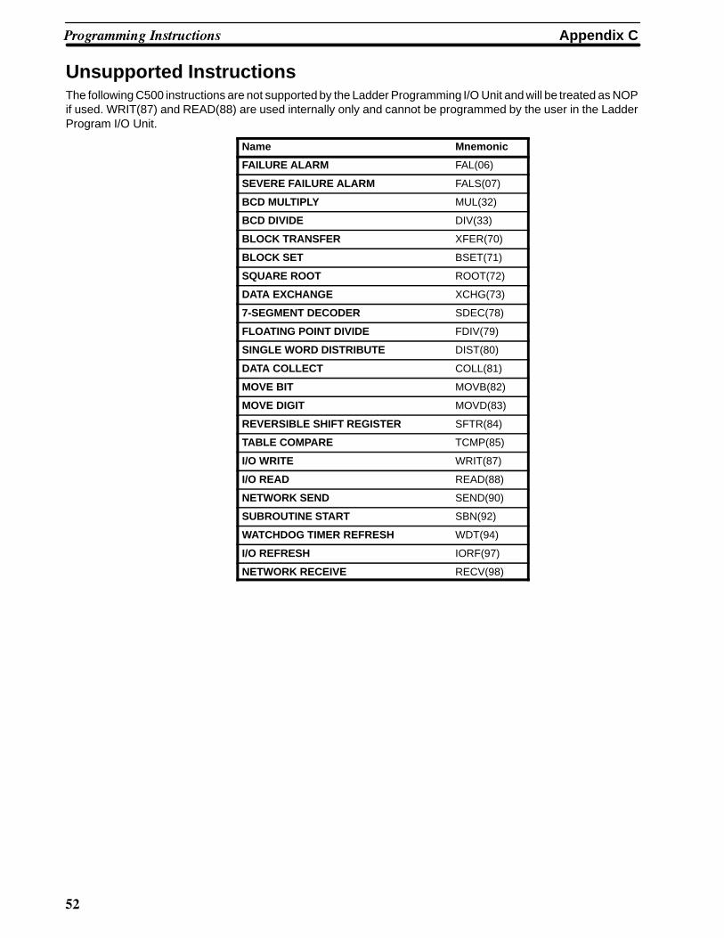
Appendix C���������� "��� �����
��
Unsupported InstructionsThe following C500 instructions are not supported by the Ladder Programming I/O Unit and will be treated as NOPif used. WRIT(87) and READ(88) are used internally only and cannot be programmed by the user in the LadderProgram I/O Unit.
Name Mnemonic
FAILURE ALARM FAL(06)
SEVERE FAILURE ALARM FALS(07)
BCD MULTIPLY MUL(32)
BCD DIVIDE DIV(33)
BLOCK TRANSFER XFER(70)
BLOCK SET BSET(71)
SQUARE ROOT ROOT(72)
DATA EXCHANGE XCHG(73)
7-SEGMENT DECODER SDEC(78)
FLOATING POINT DIVIDE FDIV(79)
SINGLE WORD DISTRIBUTE DIST(80)
DATA COLLECT COLL(81)
MOVE BIT MOVB(82)
MOVE DIGIT MOVD(83)
REVERSIBLE SHIFT REGISTER SFTR(84)
TABLE COMPARE TCMP(85)
I/O WRITE WRIT(87)
I/O READ READ(88)
NETWORK SEND SEND(90)
SUBROUTINE START SBN(92)
WATCHDOG TIMER REFRESH WDT(94)
I/O REFRESH IORF(97)
NETWORK RECEIVE RECV(98)

��
Appendix DError and Arithmetic Flag Operation
The following table shows the instructions that affect the Error (ER), Carry (CY), Greater Than (GT), Equals(EQ), and Less Than (LT) Flags. Vertical arrows in the table indicate the flags that are turned ON and OFFaccording to the result of the instruction. Instructions not shown do not affect any of the flags in the table.
In general, ER indicates that operand data is not within requirements. CY indicates arithmetic or data shift re-sults. GT indicates that a compared value is larger than some standard, LT that it is smaller, and EQ, that it isthe same. The status of these flags is maintained until another instruction that affects the flag is executed.
Although ladder diagram instructions, TIM, TIMH(15), CNT, and CNTR(12) are executed when ER is ON, oth-er instructions with a vertical arrow under the ER column are not executed if ER is ON. All of the other flags inthe following table will also not operate when ER is ON.
The status of these flags cannot be monitored from the Programming Device, because the flags are turnedOFF when the END(01) instruction is executed.
Instructions 1303 (ER) 1304 (CY) 1305 (GR) 1306 (EQ) 1307 (LE)
TIM Unaffected Unaffected Unaffected Unaffected
CNT
END(01) OFF OFF OFF OFF OFF
CNTR(12) Unaffected Unaffected Unaffected Unaffected
TIMH(15)
CMP(20) Unaffected Unaffected
MOV(21) Unaffected Unaffected Unaffected Unaffected
MVN(22)
BIN(23) Unaffected Unaffected Unaffected
BCD(24)
ASL(25) Unaffected Unaffected Unaffected
ASR(26)
ROL(27)
ROR(28)
COM(29) Unaffected Unaffected Unaffected Unaffected
ADD(30) Unaffected Unaffected
SUB(31)
ANDW(34) Unaffected Unaffected Unaffected Unaffected
ORW(35)
XORW(36)
XNRW(37)
INC(38) Unaffected Unaffected Unaffected
DEC(39)
STC(40) Unaffected ON Unaffected Unaffected Unaffected
CLC(41) Unaffected OFF Unaffected Unaffected Unaffected
SLD(74) Unaffected Unaffected Unaffected Unaffected
SRD(75)
MLPX(76)
DMPX(77)

��
���#
!"�!& ����: �1 ����: �.
!������������: �6���"�:
!����!���<��0�'/0���: �����""�����: ��
!������� ��� ���� ����
�
���� �����1: �.=�7'(: ����!��" ��"� �������������! �"��: ���������: ������� �"��: ���������: ��
�( ����: �./�: �./( 8��: �.#��& 8��: �-
���� �������: �'� #��!� ������: ��
�'� #��!�'02 ��������� ������: ��������: $: ��
�1 ����� ��� ���� ����
�
�����"��� !�� ����: 7����8"��������: �$
�������: !�������� #��� ����������: �
�'/: �
���: �-
1
<��: �
-
��������� �����: ��
��������� �����: �'� #��!� ������: ��
'02�����" ���������: ����������� 3�� ,('/).-*0(5+�)..*: �$
'02 ������: .
'02 ������ ������: �
'02 ������ ����: �
����������� ���������: �
����!��������� �����: �$�"�!���� ���������: -=��
����� 2�� ��"� : '02 ������ ����: ��
����� 2 ��"� : '02 ������ ����: ��
����""�����: !����!���: ��
�����!���� ��(5+�)..*: '02 ���������: �$��"����� #��� ����: ,('/).-*: '02 ���������: �$
�����!����: �6�!����� ����: 7
'( ����� ��� ���� ����
�
"��&�� ���������: �'� #��!� ������: ��
���: �
&
���������!�: �-
����� !���!�� :
����: !������� �"�!���: $
12 '/2( ����:
�
�����!"�����: �
"��+
�%
�
��"��� ���������� ��� ����������� ��3�!�
��������� ����: : .!�������: ����������� ���������: �"��&�� ���������:
���������: ��4 ���!����: .
������: �6�����": #��!���� !���!�� : ��
�
������� ������:
������� !���!�� :
�(2<(+1 ����:
����������� ��3�!�: ���"��� ���������: ���!������: $��"��� ����������'/0���: �<��: �
��3�!���: .
*
���� #��!�: $
(���.�� ��� !����!���
(4 ����:
�
!��: .
!�� ����: .�����: 7'02 ������ ����: �������!���� �6�!����� ����: 7
�"�!���: ������: $
��!���!�����: �6�����" '02: �
��!���!�����: ��
�( ����� ��� ���� ����
�
/� ����� ��� ���� ����
������ ��� ���� ����
/( 8��� ��� ���� ����
2
#��& 8��� ��� ���� ����
,('/).-*0(5+�)..*��� ���� �����!���� ������!� �� !�� ����: 7

%�
Revision History
A manual revision code appears as a suffix to the catalog number on the front cover of the manual.
Cat. No. W151--E1--3
Revision code
The following table outlines the changes made to the manual during each revision. Page numbers refer to theprevious version.
Revision code Date Revised content
1 February 1989 Original production (C500-LDP01)
2 June 1989 Corrections to pages 18, 22 to 26
3 January 1992 Revision for new model (C500-LDP01-V1). For a list of the differences betweenthe C500-LDP01 and the C500-LDP01-V1 refer to Section 1-3 Comparing theC500-LDP01 and the C500-LDP01-V1.