buried nmos
3
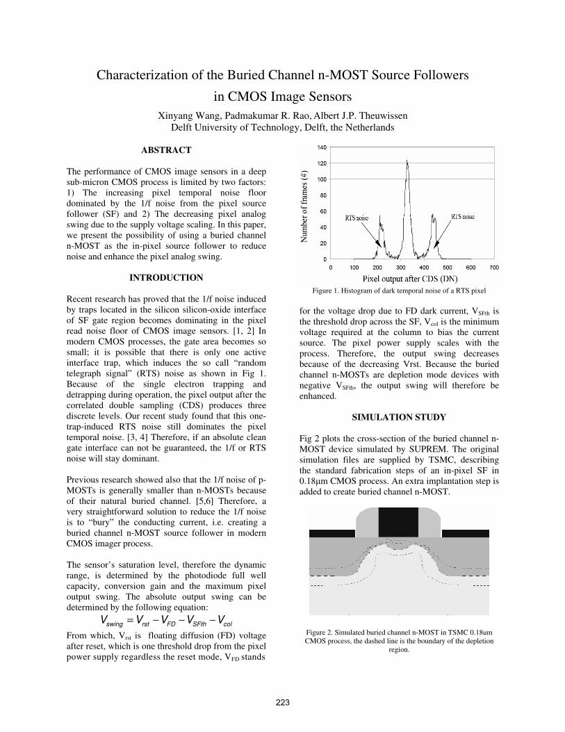
Characterization of the Buried Channel n-MOST Source Followers in CMOS Image Sensors Xinyang Wang, Padmakumar R. Rao, Albert J.P. Theuwissen Delft University of Technology, Delft, the Netherlands ABSTRACT The performance of CMOS image sensors in a deep sub-micron CMOS process is limited by two factors: 1) The increasing pixel temporal noise floor dominated by the 1/f noise from the pixel source follower (SF) and 2) The decreasing pixel analog swing due to the supply voltage scaling. In this paper, we present the possibility of using a buried channel n-MOST as the in-pixel source follower to reduce noise and enhance the pixel analog swing. INTRODUCTION Recent research has proved that the 1/f noise induced by traps located in the silicon silicon-oxide interface of SF gate region becomes dominating in the pixel read noise floor of CMOS image sensors. [1, 2] In modern CMOS processes, the gate area becomes so small; it is possible that there is only one active interface trap, which induces the so call “random telegraph signal” (RTS) noise as shown in Fig 1. Because of the single electron trapping and detrapping during operation, the pixel output after the correlated double sampling (CDS) produces three discrete levels. Our recent study found that this one- trap-induced RTS noise still dominates the pixel temporal noise. [3, 4] Therefore, if an absolute clean gate interface can not be guaranteed, the 1/f or RTS noise will stay dominant. Previous research showed also that the 1/f noise of p- MOSTs is generally smaller than n-MOSTs because of their natural buried channel. [5,6] Therefore, a very straightforward solution to reduce the 1/f noise is to “bury” the conducting current, i.e. creating a buried channel n-MOST source follower in modern CMOS imager process. The sensor’s saturation level, therefore the dynamic range, is determined by the photodiode full well capacity, conversion gain and the maximum pixel output swing. The absolute output swing can be determined by the following equation: swing rst FD SFth col V V V V V = - - - From which, V rst is floating diffusion (FD) voltage after reset, which is one threshold drop from the pixel power supply regardless the reset mode, V FD stands Figure 1. Histogram of dark temporal noise of a RTS pixel for the voltage drop due to FD dark current, V SFth is the threshold drop across the SF, V col is the minimum voltage required at the column to bias the current source. The pixel power supply scales with the process. Therefore, the output swing decreases because of the decreasing Vrst. Because the buried channel n-MOSTs are depletion mode devices with negative V SFth , the output swing will therefore be enhanced. SIMULATION STUDY Fig 2 plots the cross-section of the buried channel n- MOST device simulated by SUPREM. The original simulation files are supplied by TSMC, describing the standard fabrication steps of an in-pixel SF in 0.18μm CMOS process. An extra implantation step is added to create buried channel n-MOST. Figure 2. Simulated buried channel n-MOST in TSMC 0.18um CMOS process, the dashed line is the boundary of the depletion region. 223
-
Upload
ssyellampalli -
Category
Documents
-
view
48 -
download
7
Transcript of buried nmos
Characterization of the Buried Channel n-MOST Source Followers
in CMOS Image Sensors
Xinyang Wang, Padmakumar R. Rao, Albert J.P. Theuwissen
Delft University of Technology, Delft, the Netherlands
ABSTRACT
The performance of CMOS image sensors in a deep
sub-micron CMOS process is limited by two factors:
1) The increasing pixel temporal noise floor
dominated by the 1/f noise from the pixel source
follower (SF) and 2) The decreasing pixel analog
swing due to the supply voltage scaling. In this paper,
we present the possibility of using a buried channel
n-MOST as the in-pixel source follower to reduce
noise and enhance the pixel analog swing.
INTRODUCTION
Recent research has proved that the 1/f noise induced
by traps located in the silicon silicon-oxide interface
of SF gate region becomes dominating in the pixel
read noise floor of CMOS image sensors. [1, 2] In
modern CMOS processes, the gate area becomes so
small; it is possible that there is only one active
interface trap, which induces the so call “random
telegraph signal” (RTS) noise as shown in Fig 1.
Because of the single electron trapping and
detrapping during operation, the pixel output after the
correlated double sampling (CDS) produces three
discrete levels. Our recent study found that this one-
trap-induced RTS noise still dominates the pixel
temporal noise. [3, 4] Therefore, if an absolute clean
gate interface can not be guaranteed, the 1/f or RTS
noise will stay dominant.
Previous research showed also that the 1/f noise of p-
MOSTs is generally smaller than n-MOSTs because
of their natural buried channel. [5,6] Therefore, a
very straightforward solution to reduce the 1/f noise
is to “bury” the conducting current, i.e. creating a
buried channel n-MOST source follower in modern
CMOS imager process.
The sensor’s saturation level, therefore the dynamic
range, is determined by the photodiode full well
capacity, conversion gain and the maximum pixel
output swing. The absolute output swing can be
determined by the following equation:
swing rst FD SFth colV V V V V= − − −
From which, Vrst is floating diffusion (FD) voltage
after reset, which is one threshold drop from the pixel
power supply regardless the reset mode, VFD stands
Figure 1. Histogram of dark temporal noise of a RTS pixel
for the voltage drop due to FD dark current, VSFth is
the threshold drop across the SF, Vcol is the minimum
voltage required at the column to bias the current
source. The pixel power supply scales with the
process. Therefore, the output swing decreases
because of the decreasing Vrst. Because the buried
channel n-MOSTs are depletion mode devices with
negative VSFth, the output swing will therefore be
enhanced.
SIMULATION STUDY
Fig 2 plots the cross-section of the buried channel n-
MOST device simulated by SUPREM. The original
simulation files are supplied by TSMC, describing
the standard fabrication steps of an in-pixel SF in
0.18µm CMOS process. An extra implantation step is
added to create buried channel n-MOST.
Figure 2. Simulated buried channel n-MOST in TSMC 0.18um
CMOS process, the dashed line is the boundary of the depletion
region.
223

As shown in the Fig 2, a fully-depleted gate interface
can be achieved at zero volt gate bias condition. The
max channel potential and buried depth are
determined by the doping energy and dose.
Test structures have been fabricated in TSMC
0.18µm CMOS process with five different buried
channel implant energy and dose combinations. Fig 3
is a comparison of the simulated and the measured
gate characteristic of the buried channel transistors.
As expected, increasing the implantation dose will
shift the transistor threshold voltage towards negative.
As shown, the extracted threshold voltages are less
negative than the simulated ones; the difference is
bigger for higher implant doses. Increasing
implantation energy will slightly increase the channel
depth, however, with the penalty of a large leakage
current. Therefore, the implantation dose and energy
need to be adjusted carefully to obtain an optimized
channel depth and threshold voltage.
Figure 3. Simulation and measurement of the gate characteristic for
different buried channel n-MOSTs, with same implant energy but
different doses
MEASUREMENT RESULTS
Both single transistors and pixel test structures were
fabricated for measurements and characterizations.
Fig 4 is the schematic of the pixel test structure and
the column bias circuitry used to measure the pixel
output swing. The pixel is a standard pinned 4T
design without the row select transistor.
Fig 5 plots the measurement results of the absolute
pixel output swing. During the measurement, the
reset transistor (RST) gate is tied to the highest
voltage of the pixel, i.e. performing hard reset, and
the transfer gate is switched off. Therefore, the FD
voltage equals the reset transistor power supply. The
column bias current is 6uA for all pixels. As shown,
because of pixel output swing improves drastically.
Figure 4. Pixel schematic and column bias circuitry with buried
source follower (BSF), reset transistor (RST), transfer gate (TG),
pinned photodiode (PPD) and separated power supply to the BSF
(Vdd_bsf) and RST (Vdd_rst)
Figure 5. Measurement of the absolute pixel output swing, pixels
with standard SF and BSF
Interestingly, from Fig 5, we are also able to observe
an improved voltage gain for buried channel device,
(>0.9) compare to the standard surface mode device
(0.83).
Fig 6 is the 1/f noise measurement setup for single
transistors. The DUT is biased as the source follower
operation with the drain tied to 3.3V and 6uA
conducting current. The gate of the DUT is biased by
a normal DC source with a 1Hz filter in order to
block all AC components. The drain is tied to a
battery power supply. The conducting current is
compensated by a battery powered current source.
The test devices and the battery are in a sealed box.
Fig 7 plots the measured 1/f noise power spectrum
density of a surface and a buried channel test device
with the same dimensions. We find that the slope of
the curves for buried channel devices are normally
between -0.6 and -0.8, which indicates a different
noise mechanism from the surface origin of the
standard n-MOSTs. As shown, the low frequency
noise of the buried channel device is significantly
224

Figure 6. 1/f noise measurement setup for buried / surface channel
n-MOSTs under source follower bias condition
reduced. However, the 1/f dominated read noise of
CMOS imagers is the product of the 1/f PSD and the
CDS transfer function. Therefore, the noise reduction
efficiency highly depends on the CDS period as well
as the frequency of the crossing point is Fig 7.
Complete image sensor with BSFs was made. The
pixel pitch is 7.4µm, with power supply of 3.3V. Fig
8 is the dark random noise measurement histogram.
The random noise of each pixel is taken by
calculating the standard deviation of the pixel outputs
through 20 frames. The measurement is done in
complete dark. In order to exclude the dark current
shot noise effect, the transfer gate is switched off
during two sample and hold periods of the CDS.
Figure 7. 1/f noise measurement for surface/buried n-MOSTs
The histogram is plotted in linear scale in order to
highlight the noise improvement of the majority
pixels instead of those “hot” ones. As shown, both
the mean and the σ value of BSF pixels’ noise are
reduced.
CONCLUSIONS
Figure 8.Dark random noise histogram for buried/surface SF pixels
Buried channel n-MOSTs are successfully made
through deep sub-micron CMOS process and being
characterized regarding their source follower
application in CMOS image sensor pixels Because of
a ‘buried’ conducting current, the following
advantages are reported from the our measurement
and characterizations: 1) 1/f noise is significantly
reduced. 2) The pixel output swing is enhanced
drastically. 3) The SF voltage gain is increased.
ACKNOWLEDGEMENT
The authors would like to thank the CMOS imager
group of DALSA BV for their helps on designing the
test sensor, and TSMC for their generous offer to
make this research possible. This work is sponsored
by the Dutch Technology Foundation (STW).
REFERENCES
[1] Bedabrata Pain et.al. “Excess noise and dark
current mechanisms in CMOS imagers”, pp145-148,
IEEE Workshop on CCDs & AIS, June 2005
[2] Jung Yeon Kim et.al., “Characterization and
improvement of random noise in 1/3.2” UXGA
CMOS image sensor with 2.8um pixel using 0.13-
technology” pp149-152, IEEE Workshop on CCDs &
AIS, June 2005
[3] Xinyang Wang et.al. “Random telegraph signal in
CMOS image sensor pixels”, pp115-118, IEDM, Dec
2006
[4] Leyris C et.al. “Impact of random telegraph signal
in CMOS image sensors for low-light levels”, pp276-
379, ESSCIRC, Sep 2006.
[5] L.L.J.Vandamme et.al, “1/f noise in MOS devices,
mobility or number fluctuations” IEEE Trans on
Electron Device, Vol. 41, pp1936-1945, Nov, 1994
[6] Jimmin Chang et.al, “Flicker Noise in CMOS
Transistors from subthreshold to strong inversion at
various temperatures” IEEE Trans on Electron
Device, Vol. 41, pp1965-1971, Nov 1994
225