Bruce Jacob ENEE 359a University of Digital VLSI Design ... 4 UNIVERSITY OF MARYLAND ... • To...
33
ENEE 359a Lecture/s 23-25 DRAM Circuits Bruce Jacob University of Maryland ECE Dept. SLIDE 1 UNIVERSITY OF MARYLAND ENEE 359a Digital VLSI Design CMOS Memories and Systems: Part II, DRAM Circuits Prof. Bruce Jacob [email protected] Credit where credit is due: Slides contain original artwork (© Jacob 1999–2004, Wang 2003/4) as well as material taken from Keeth & Baker’s DRAM Circuit Design .
Transcript of Bruce Jacob ENEE 359a University of Digital VLSI Design ... 4 UNIVERSITY OF MARYLAND ... • To...
ENEE 359aLecture/s 23-25
DRAM Circuits
Bruce Jacob
University ofMaryland
ECE Dept.
SLIDE 1
UNIVERSITY OF MARYLAND
ENEE 359a
Digital VLSI Design
CMOS Memories and Systems: Part II, DRAM Cir cuits
Prof . Bruce [email protected]
Credit where credit is due:
Slides contain original artwork (© Jacob 1999–2004, Wang 2003/4) as well as material taken from Keeth & Baker’s DRAM Circuit Design.
ENEE 359aLecture/s 23-25
DRAM Circuits
Bruce Jacob
University ofMaryland
ECE Dept.
SLIDE 2
UNIVERSITY OF MARYLAND
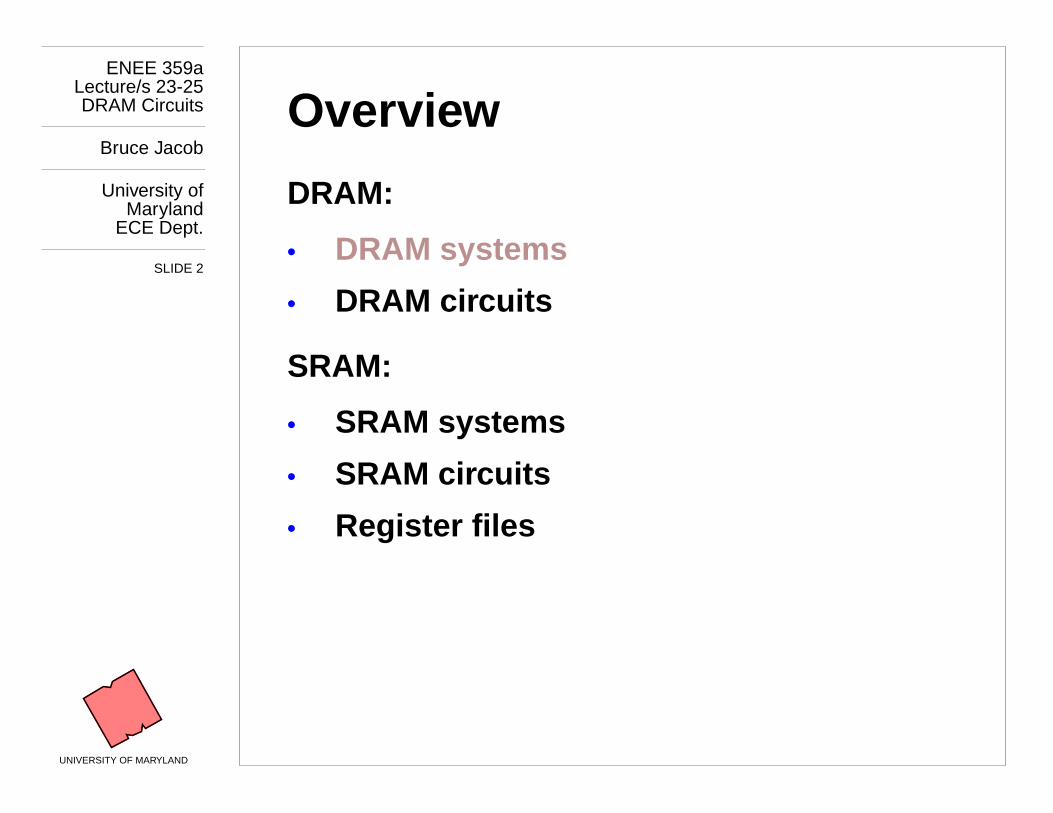
Overview
DRAM:
•
DRAM systems
•
DRAM cir cuits
SRAM:
•
SRAM systems
•
SRAM cir cuits
•
Register fi les
ENEE 359aLecture/s 23-25
DRAM Circuits
Bruce Jacob
University ofMaryland
ECE Dept.
SLIDE 3
UNIVERSITY OF MARYLAND
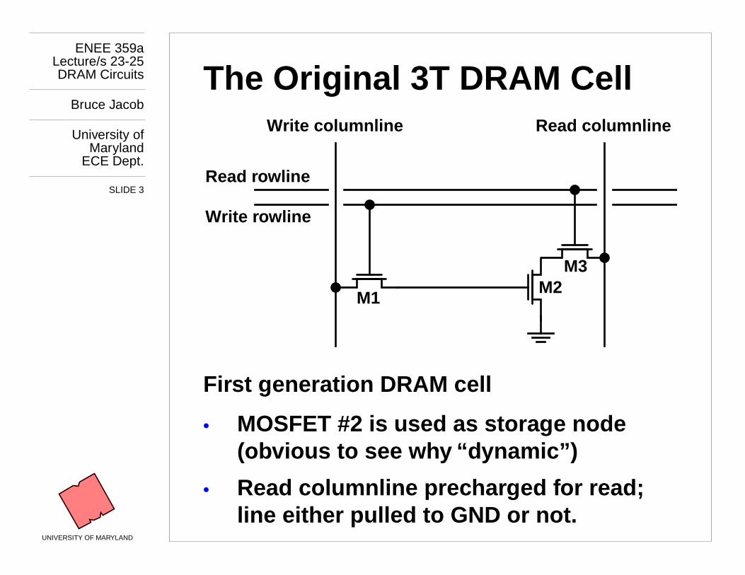
The Original 3T DRAM Cell
First g eneration DRAM cell
•
MOSFET #2 is used as stora ge node(obvious to see wh y “d ynamic”)
•
Read columnline prec harged for read; line either pulled to GND or not.
M1M2
M3
Read rowline
Write r owline
Write columnline Read columnline
ENEE 359aLecture/s 23-25
DRAM Circuits
Bruce Jacob
University ofMaryland
ECE Dept.
SLIDE 4
UNIVERSITY OF MARYLAND
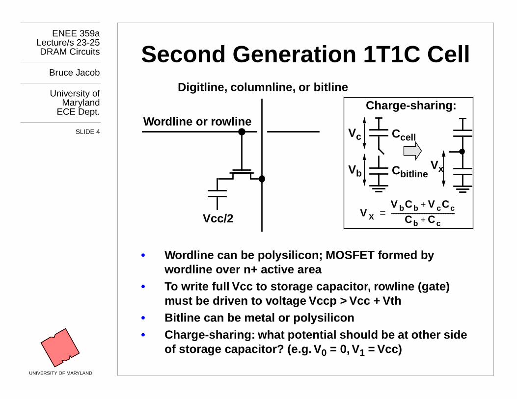
Second Generation 1T1C Cell
• Wordline can be pol ysilicon; MOSFET formed b y wordline o ver n+ active area
• To write full Vcc to stora ge capacitor , rowline (gate) must be driven to v olta ge Vccp > Vcc + Vth
• Bitline can be metal or pol ysilicon • Charge-sharing: what potential should be at other side
of stora ge capacitor? (e .g. V
0
= 0, V
1
= Vcc)
Wordline or r owline
Digitline , columnline , or bitline
Vcc/2
Charge-sharing:
C
cell
C
bitline
V
c
V
b
V
x
V
X
V
b
C
b
V
c
C
c
+
C
b
C
c
+
-------------------------------------=
ENEE 359aLecture/s 23-25
DRAM Circuits
Bruce Jacob
University ofMaryland
ECE Dept.
SLIDE 5
UNIVERSITY OF MARYLAND
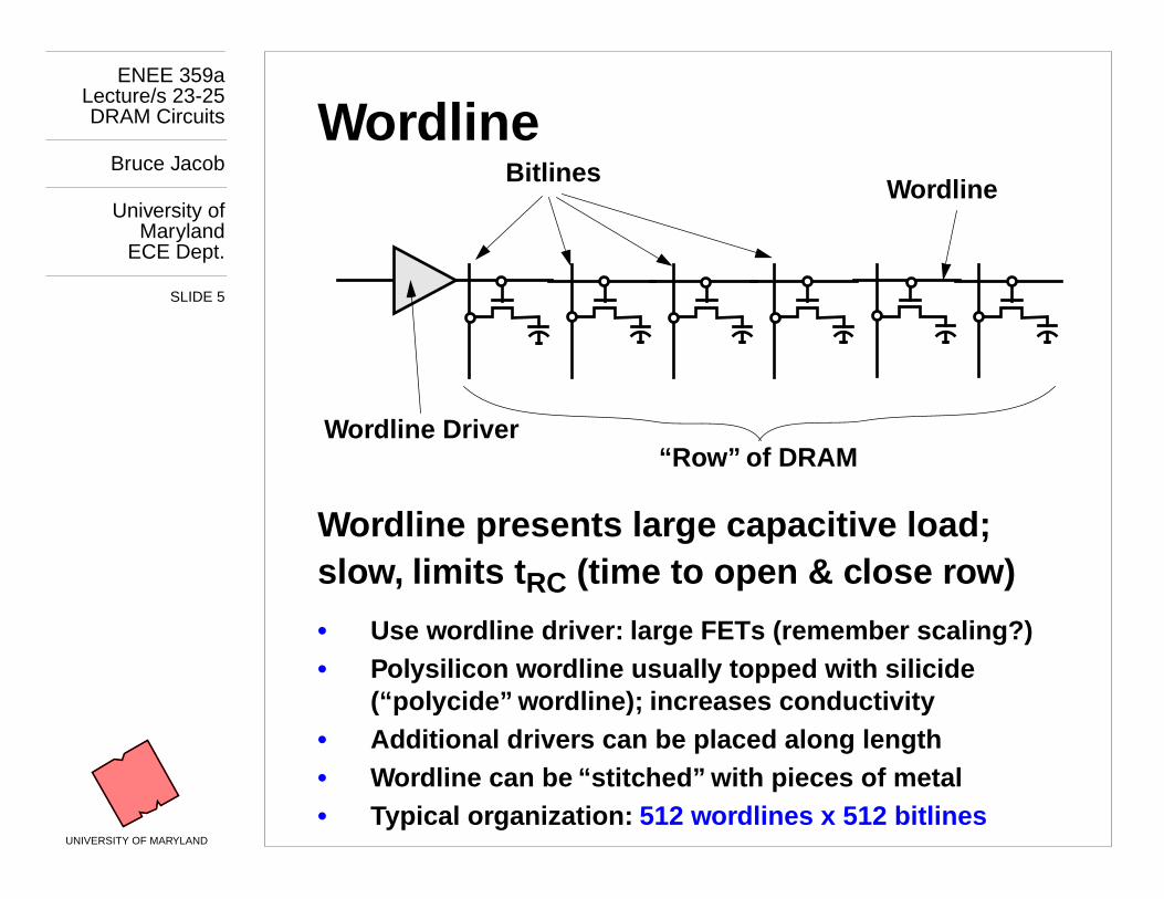
Wordline
Wordline presents lar ge capacitive load; slo w, limits t
RC
(time to open & c lose r ow)
• Use wordline driver: large FETs (remember scaling?)• Polysilicon w ordline usuall y topped with silicide
(“pol ycide” wordline); increases conductivity• Additional driver s can be placed along length• Wordline can be “stitc hed” with pieces of metal• Typical or ganization: 512 wordlines x 512 bitlines
BitlinesWordline
“Ro w” of DRAMWordline Driver
ENEE 359aLecture/s 23-25
DRAM Circuits
Bruce Jacob
University ofMaryland
ECE Dept.
SLIDE 6
UNIVERSITY OF MARYLAND
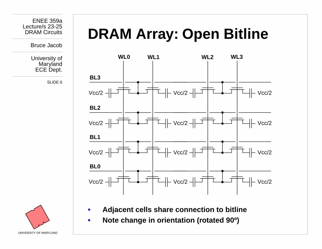
DRAM Arra y: Open Bitline
• Adjacent cells share connection to bitline• Note c hang e in orientation (r otated 90º)
Vcc/2 Vcc/2
BL3
Vcc/2
WL0 WL1 WL2 WL3
Vcc/2 Vcc/2
BL2
Vcc/2
Vcc/2 Vcc/2
BL1
Vcc/2
Vcc/2 Vcc/2
BL0
Vcc/2
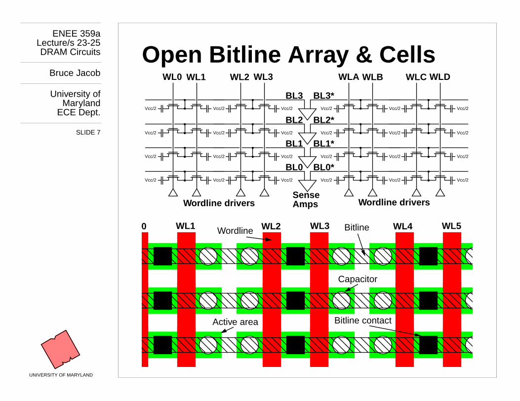
ENEE 359aLecture/s 23-25
DRAM Circuits
Bruce Jacob
University ofMaryland
ECE Dept.
SLIDE 7
UNIVERSITY OF MARYLAND
Open Bitline Arra y & Cells
Vcc/2 Vcc/2
BL3
Vcc/2
WL0 WL1 WL2 WL3
Vcc/2 Vcc/2
BL2
Vcc/2
Vcc/2 Vcc/2
BL1
Vcc/2
Vcc/2 Vcc/2
BL0
Vcc/2
Vcc/2 Vcc/2
BL3*
Vcc/2
WLA WLB WLC WLD
Vcc/2 Vcc/2
BL2*
Vcc/2
Vcc/2 Vcc/2
BL1*
Vcc/2
Vcc/2 Vcc/2
BL0*
Vcc/2
Wordline driver s Wordline driver sSenseAmps
WL2 WL3 WL4 WL5WL0 WL1
Wordline Bitline
Active area
Capacitor
Bitline contact
ENEE 359aLecture/s 23-25
DRAM Circuits
Bruce Jacob
University ofMaryland
ECE Dept.
SLIDE 8
UNIVERSITY OF MARYLAND
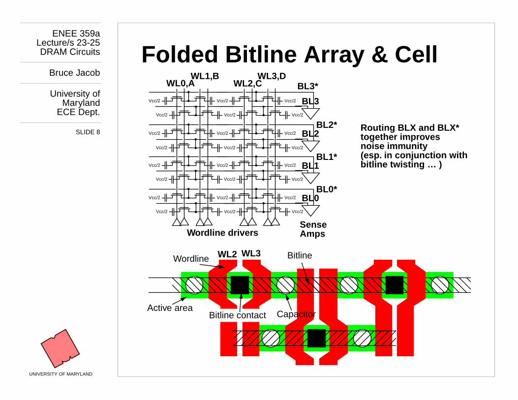
Folded Bitline Arra y & Cell
Vcc/2 Vcc/2
BL3*
Vcc/2
WL0,AWL1,B
WL2,CWL3,D
Wordline driver sSenseAmps
Vcc/2 Vcc/2 Vcc/2
BL3
Vcc/2 Vcc/2
BL2*
Vcc/2
Vcc/2 Vcc/2 Vcc/2
BL2
Vcc/2 Vcc/2
BL1*
Vcc/2
Vcc/2 Vcc/2 Vcc/2
BL1
Vcc/2 Vcc/2
BL0*
Vcc/2
Vcc/2 Vcc/2 Vcc/2
BL0
Routing BLX and BLX*tog ether impr oves noise imm unity(esp. in conjunction with
bitline twisting …
)
WL2 WL3
Wordline Bitline
Active areaCapacitorBitline contact
ENEE 359aLecture/s 23-25
DRAM Circuits
Bruce Jacob
University ofMaryland
ECE Dept.
SLIDE 9
UNIVERSITY OF MARYLAND
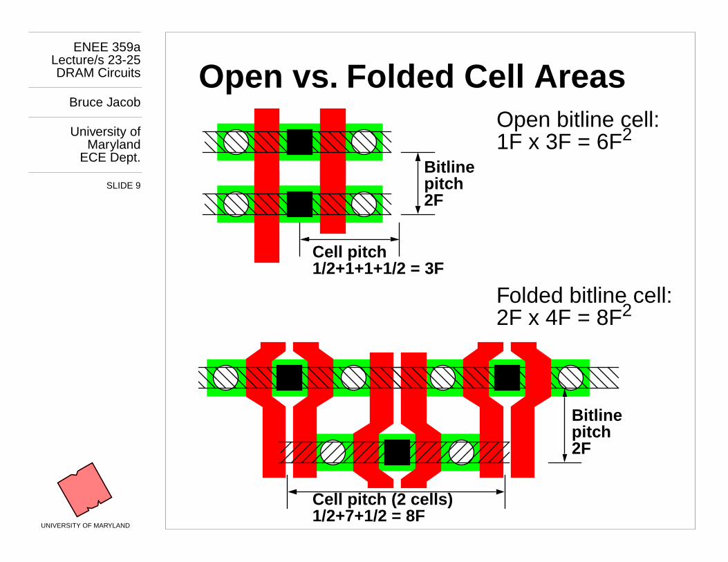
Open vs. Folded Cell Areas
Bitline pitc h2F
Cell pitc h1/2+1+1+1/2 = 3F
Open bitline cell:1F x 3F = 6F
2
Folded bitline cell:2F x 4F = 8F
2
Bitline pitc h2F
Cell pitc h (2 cells)1/2+7+1/2 = 8F
ENEE 359aLecture/s 23-25
DRAM Circuits
Bruce Jacob
University ofMaryland
ECE Dept.
SLIDE 10
UNIVERSITY OF MARYLAND
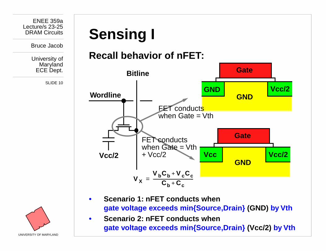
Sensing I
Recall beha vior of nFET :
• Scenario 1: nFET conducts whengate volta ge exceeds min{Sour ce,Drain} (GND) by Vth
• Scenario 2: nFET conducts when gate volta ge exceeds min{Sour ce,Drain} (Vcc/2) by Vth
Wordline
Bitline
Vcc/2
GND Vcc/2
Gate
GND
Vcc Vcc/2
Gate
GND
FET conductswhen Gate = Vth
FET conductswhen Gate = Vth+ Vcc/2
V
X
V
b
C
b
V
c
C
c
+
C
b
C
c
+
-------------------------------------=
ENEE 359aLecture/s 23-25
DRAM Circuits
Bruce Jacob
University ofMaryland
ECE Dept.
SLIDE 11
UNIVERSITY OF MARYLAND
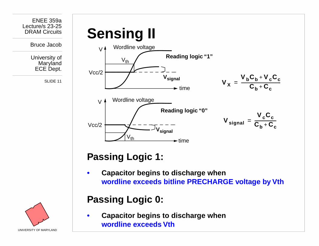
Sensing II
Passing Logic 1:
• Capacitor begins to disc harge when wordline e xceeds bitline PRECHARGE v olta ge by Vth
Passing Logic 0:
• Capacitor begins to disc harge when wordline e xceeds Vth
V
time
Vcc/2
Reading logic “1”
V
time
Vcc/2
Reading logic “0”
V
th
V
th
Wordline voltage
Wordline voltage
V
signal
V
c
C
c
C
b
C
c
+
--------------------=
V
X
V
b
C
b
V
c
C
c
+
C
b
C
c
+
-------------------------------------=
V
signal
V
signal
ENEE 359aLecture/s 23-25
DRAM Circuits
Bruce Jacob
University ofMaryland
ECE Dept.
SLIDE 12
UNIVERSITY OF MARYLAND
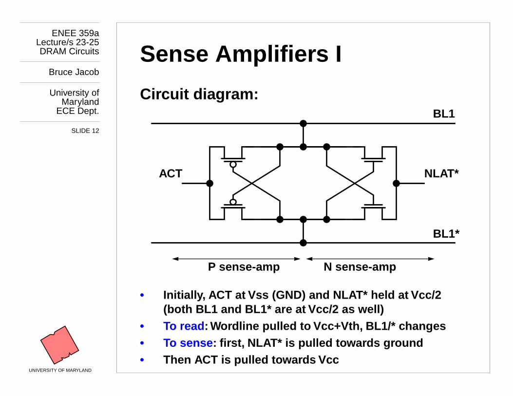
Sense Amplifi ers I
Circuit dia gram:
• Initiall y, ACT at Vss (GND) and NLA T* held at Vcc/2(both BL1 and BL1* are at Vcc/2 as well)
• To read : Wordline pulled to Vcc+Vth, BL1/* c hang es• To sense : first, NLAT* is pulled to wards gr ound• Then ACT is pulled to wards Vcc
NLAT*ACT
BL1
BL1*
N sense-ampP sense-amp
ENEE 359aLecture/s 23-25
DRAM Circuits
Bruce Jacob
University ofMaryland
ECE Dept.
SLIDE 13
UNIVERSITY OF MARYLAND
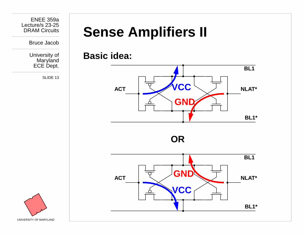
Sense Amplifi ers II
Basic idea:
NLAT*ACT
BL1
BL1*
NLAT*ACT
BL1
BL1*
OR
VCC
VCC
GND
GND
ENEE 359aLecture/s 23-25
DRAM Circuits
Bruce Jacob
University ofMaryland
ECE Dept.
SLIDE 14
UNIVERSITY OF MARYLAND
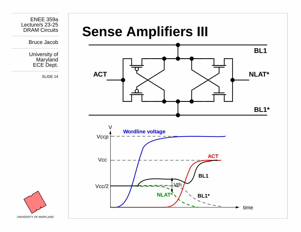
Sense Amplifi ers III
NLAT*ACT
BL1
BL1*
V
time
Vcc/2
Wordline v olta ge
Vcc
Vccp
NLAT*
ACT
BL1
BL1*
Vth
ENEE 359aLecture/s 23-25
DRAM Circuits
Bruce Jacob
University ofMaryland
ECE Dept.
SLIDE 15
UNIVERSITY OF MARYLAND
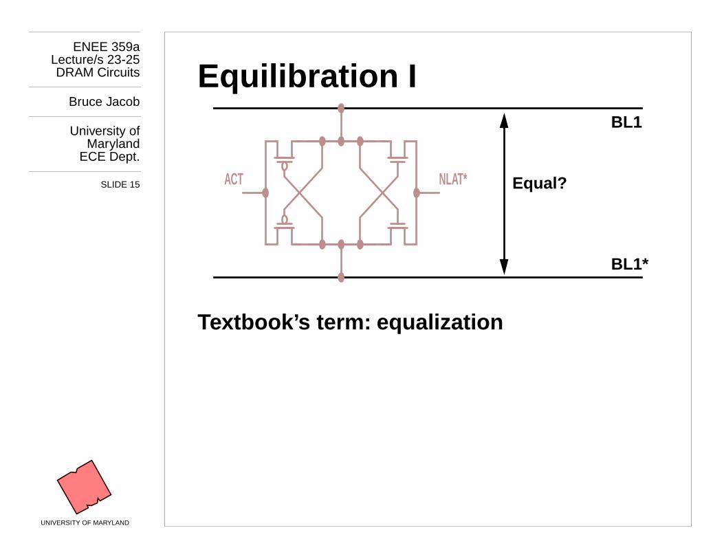
Equilibration I
Textbook’ s term:
equalization
NLAT*ACT
BL1
BL1*
Equal?
ENEE 359aLecture/s 23-25
DRAM Circuits
Bruce Jacob
University ofMaryland
ECE Dept.
SLIDE 16
UNIVERSITY OF MARYLAND
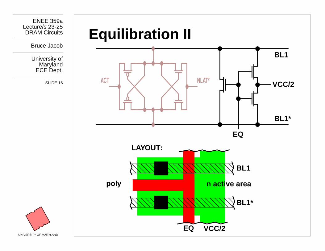
Equilibration II
NLAT*ACT
BL1
BL1*
VCC/2
EQ
n active area
LAYOUT:
pol y
EQ VCC/2
BL1
BL1*
ENEE 359aLecture/s 23-25
DRAM Circuits
Bruce Jacob
University ofMaryland
ECE Dept.
SLIDE 17
UNIVERSITY OF MARYLAND
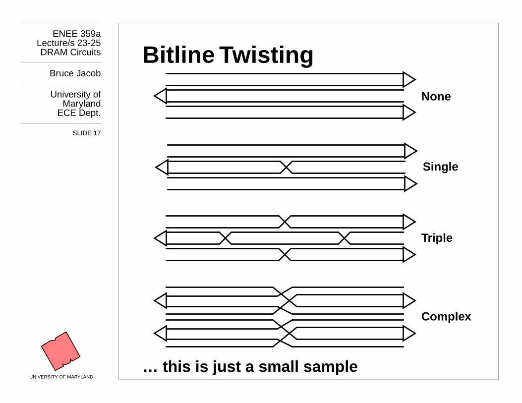
Bitline Twisting
… this is just a small sample
None
Single
Triple
Comple x
ENEE 359aLecture/s 23-25
DRAM Circuits
Bruce Jacob
University ofMaryland
ECE Dept.
SLIDE 18
UNIVERSITY OF MARYLAND
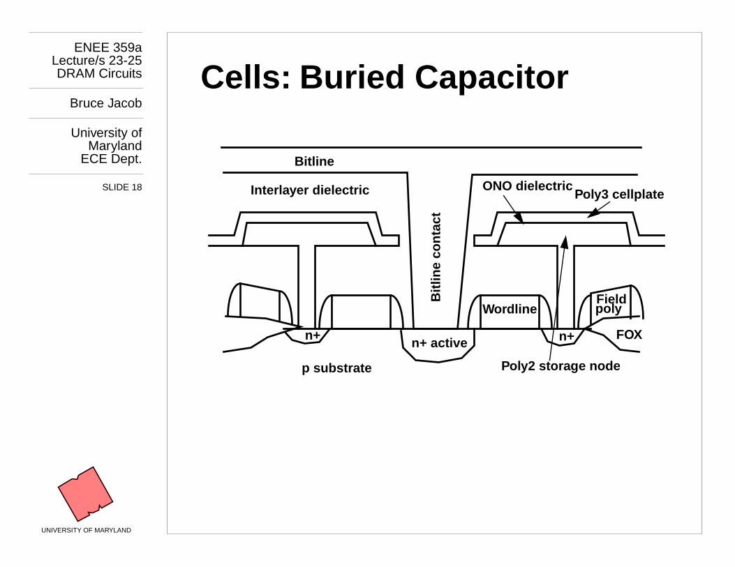
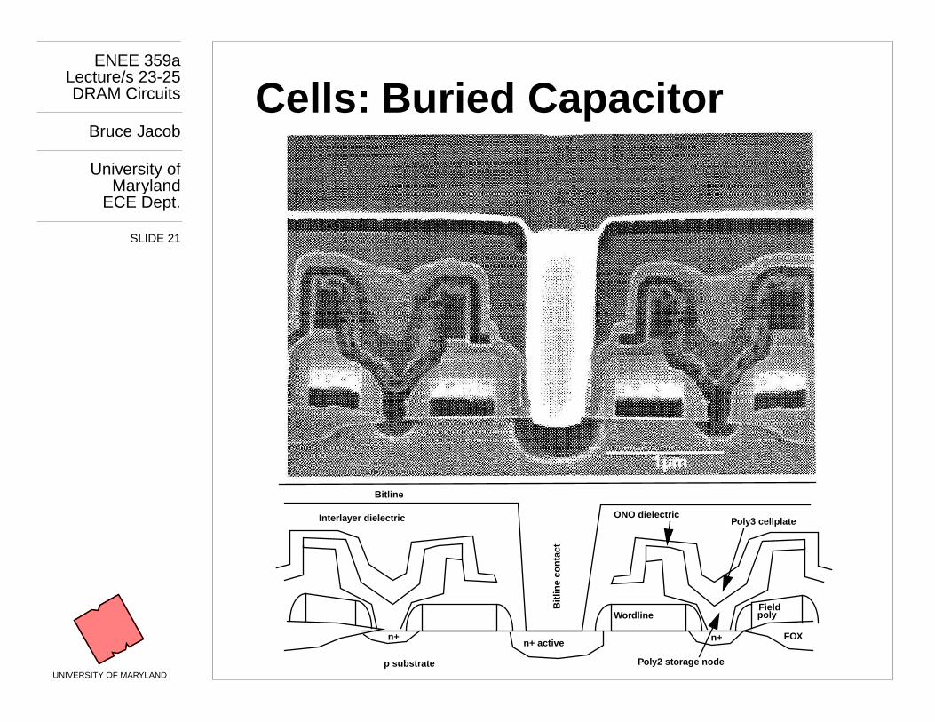
Cells: Buried Capacitor
Bitline
Bitl
ine
cont
act
Interla yer dielectric ONO dielectricPoly3 cellplate
Wordline
n+ activeFOX
Fieldpol y
p substrate Poly2 stora ge node
n+ n+
ENEE 359aLecture/s 23-25
DRAM Circuits
Bruce Jacob
University ofMaryland
ECE Dept.
SLIDE 19
UNIVERSITY OF MARYLAND
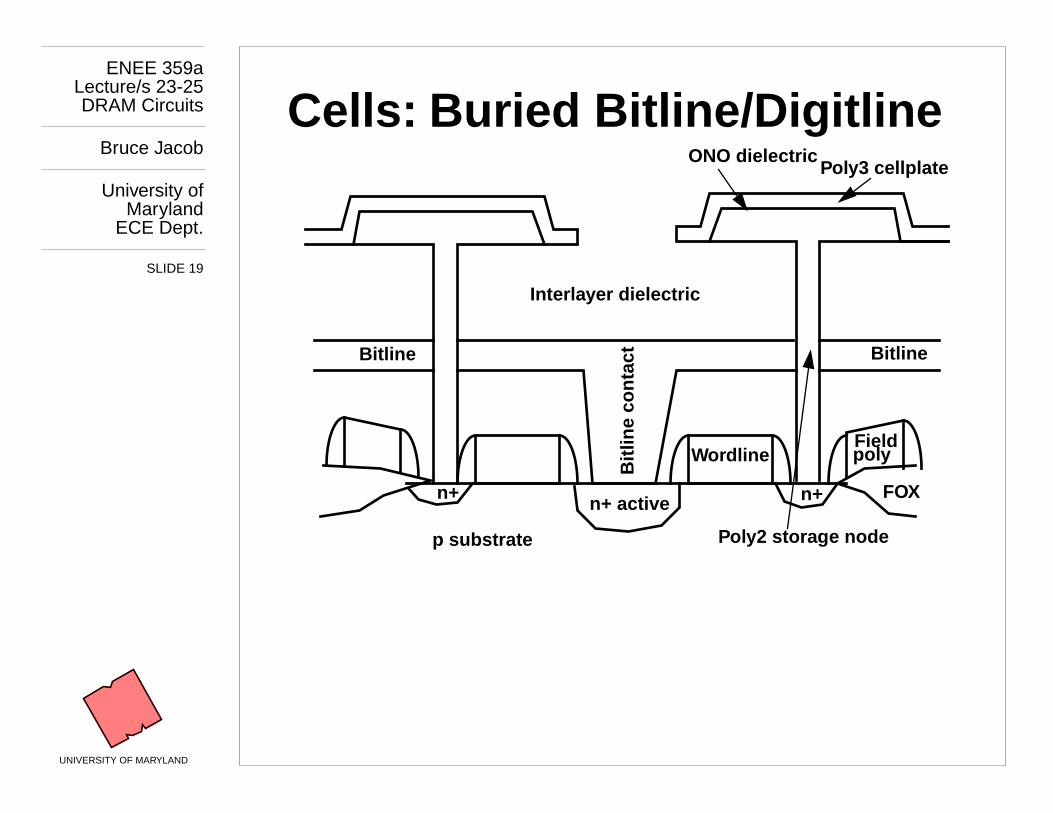
Cells: Buried Bitline/Digitline
Bitline
Bitl
ine
cont
act
Interla yer dielectric
ONO dielectricPoly3 cellplate
Wordline
n+ activeFOX
Fieldpol y
p substrate Poly2 stora ge node
n+ n+
Bitline
ENEE 359aLecture/s 23-25
DRAM Circuits
Bruce Jacob
University ofMaryland
ECE Dept.
SLIDE 20
UNIVERSITY OF MARYLAND
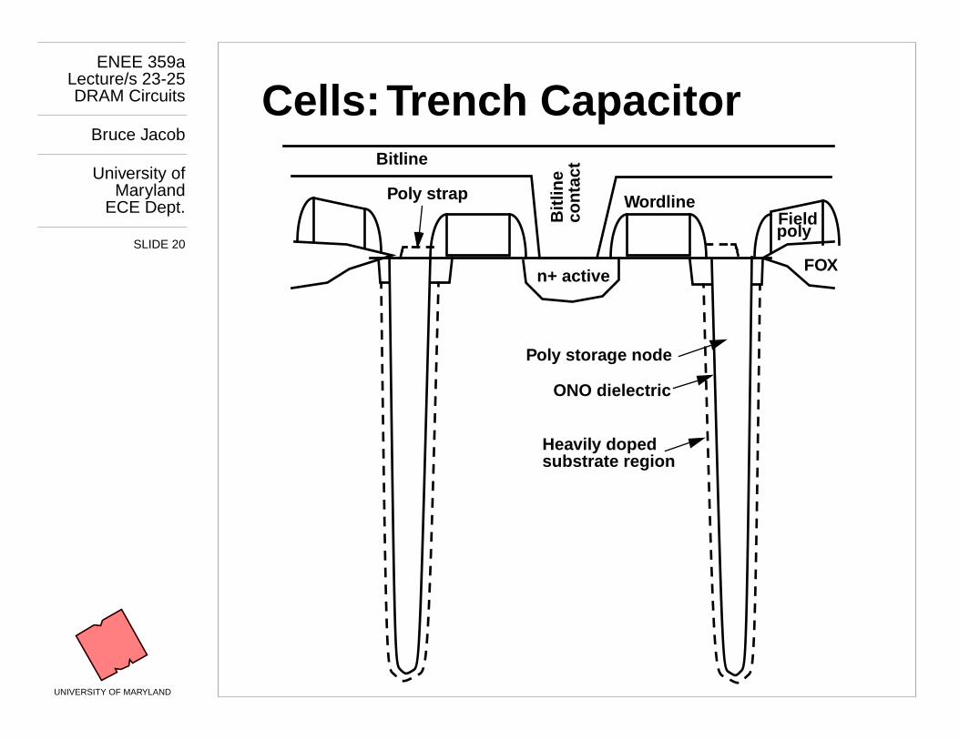
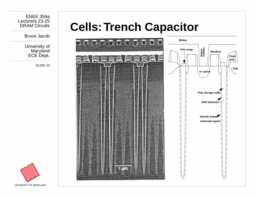
Cells: Trenc h Capacitor
Bitline
Bitl
ine
ONO dielectric
Heavil y doped
Wordline
n+ activeFOX
Fieldpol y
Poly stora ge node
cont
act
substrate region
Poly strap
ENEE 359aLecture/s 23-25
DRAM Circuits
Bruce Jacob
University ofMaryland
ECE Dept.
SLIDE 21
UNIVERSITY OF MARYLAND
Cells: Buried Capacitor
Bitline
Bitl
ine
cont
act
Interla yer dielectric ONO dielectricPoly3 cellplate
Wordline
n+ activeFOX
Fieldpol y
p substrate Poly2 stora ge node
n+ n+
ENEE 359aLecture/s 23-25
DRAM Circuits
Bruce Jacob
University ofMaryland
ECE Dept.
SLIDE 22
UNIVERSITY OF MARYLAND
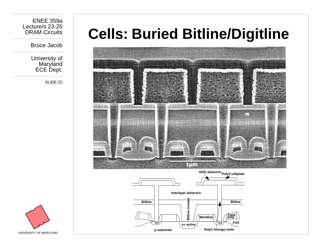
Cells: Buried Bitline/Digitline
Bitline
Bitl
ine
cont
act
Interla yer dielectric
ONO dielectric Poly3 cellplate
Wordline
n+ active FOX
Fieldpol y
p substrate Poly2 stora ge node
n+ n+
Bitline
ENEE 359aLecture/s 23-25
DRAM Circuits
Bruce Jacob
University ofMaryland
ECE Dept.
SLIDE 23
UNIVERSITY OF MARYLAND
Cells: Trenc h Capacitor
Bitline
Bitl
ine
ONO dielectric
Heavil y doped
Wordline
n+ activeFOX
Fieldpol y
Poly stora ge node
cont
act
substrate region
Poly strap
ENEE 359aLecture/s 23-25
DRAM Circuits
Bruce Jacob
University ofMaryland
ECE Dept.
SLIDE 24
UNIVERSITY OF MARYLAND
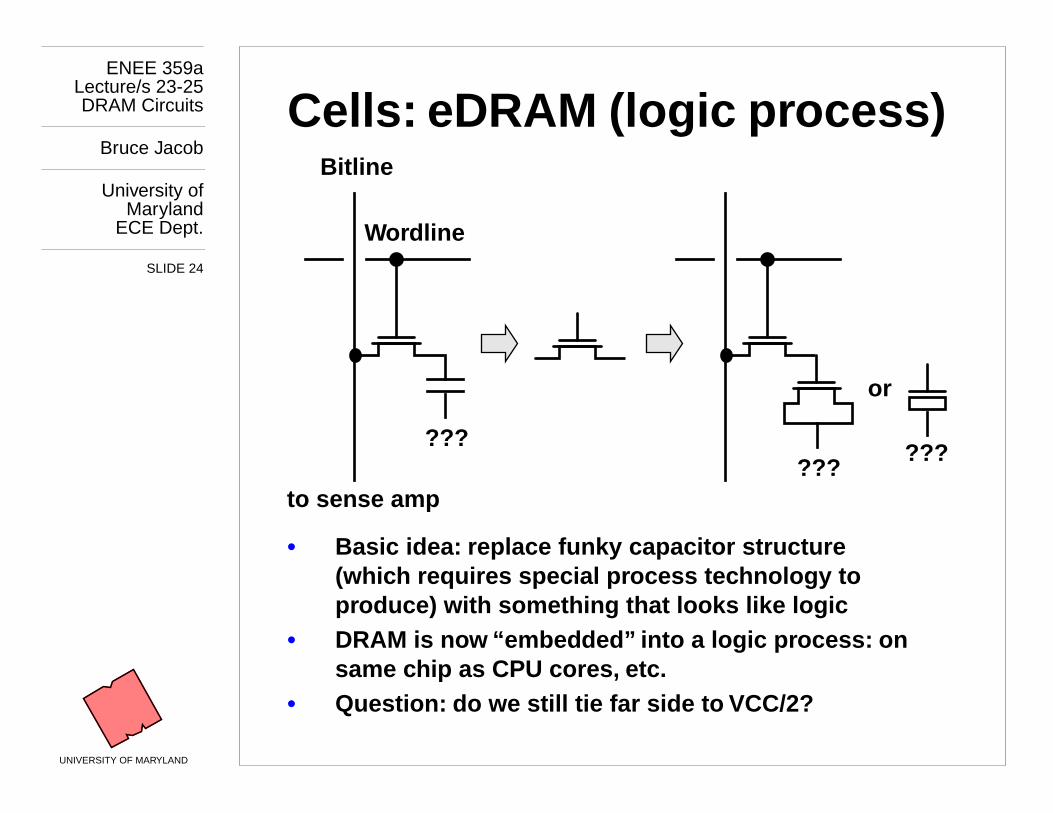
Cells: eDRAM (logic pr ocess)
• Basic idea: replace funky capacitor structure (whic h requires special pr ocess tec hnology to produce) with something that looks like logic
• DRAM is no w “embed ded” into a logic pr ocess: on same c hip as CPU cores, etc.
• Question: do we still tie far side to VCC/2?
Wordline
Bitline
??????
to sense amp
???
or
ENEE 359aLecture/s 23-25
DRAM Circuits
Bruce Jacob
University ofMaryland
ECE Dept.
SLIDE 25
UNIVERSITY OF MARYLAND
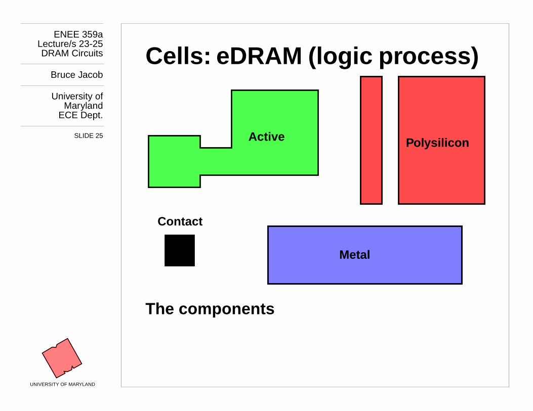
Cells: eDRAM (logic pr ocess)
The components
Active Polysilicon
Metal
Contact
ENEE 359aLecture/s 23-25
DRAM Circuits
Bruce Jacob
University ofMaryland
ECE Dept.
SLIDE 26
UNIVERSITY OF MARYLAND
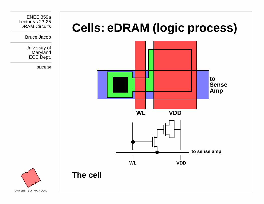
Cells: eDRAM (logic pr ocess)
The cell
VDDWL
toSenseAmp
to sense amp
WL VDD
ENEE 359aLecture/s 23-25
DRAM Circuits
Bruce Jacob
University ofMaryland
ECE Dept.
SLIDE 27
UNIVERSITY OF MARYLAND
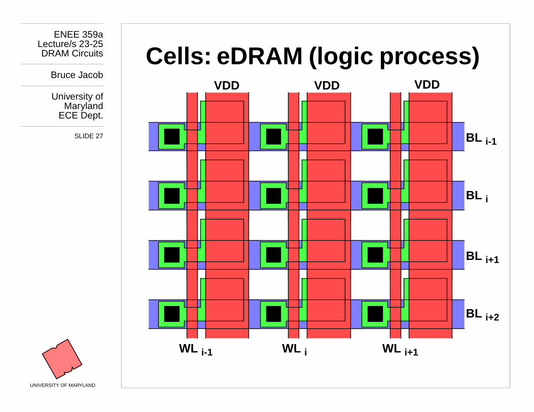
Cells: eDRAM (logic pr ocess)
VDD
WL
i-1
VDDVDD
WL
i
WL
i+1
BL
i
BL
i-1
BL
i+1
BL
i+2
ENEE 359aLecture/s 23-25
DRAM Circuits
Bruce Jacob
University ofMaryland
ECE Dept.
SLIDE 28
UNIVERSITY OF MARYLAND
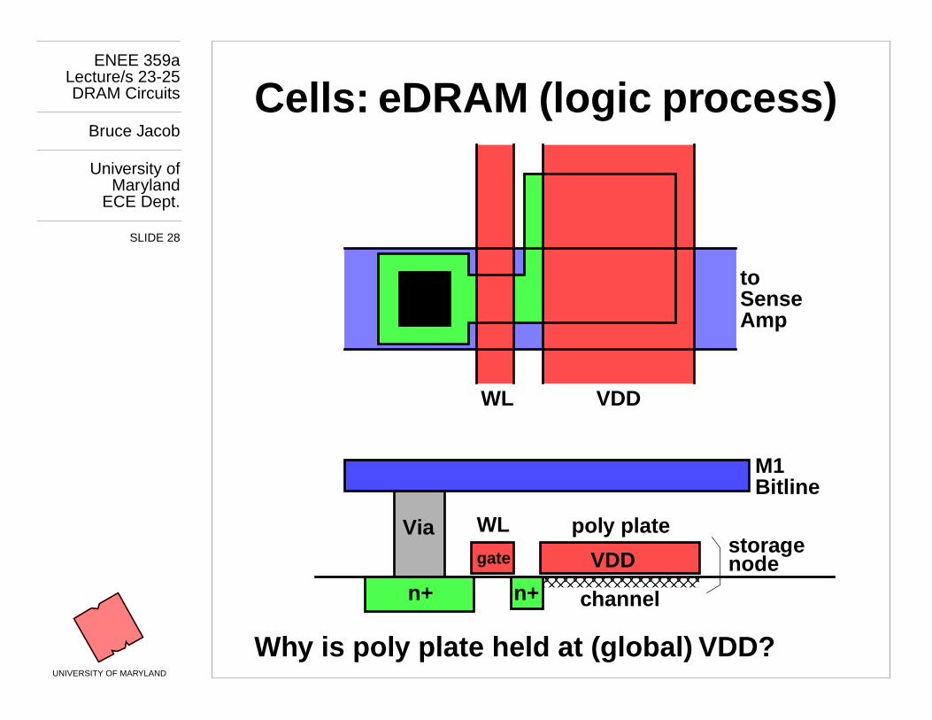
Cells: eDRAM (logic pr ocess)
Why is pol y plate held at (global) VDD?
VDDWL
toSenseAmp
M1Bitline
Via
n+ n+
WL pol y plate
channel
stora genodeVDD
gate
ENEE 359aLecture/s 23-25
DRAM Circuits
Bruce Jacob
University ofMaryland
ECE Dept.
SLIDE 29
UNIVERSITY OF MARYLAND
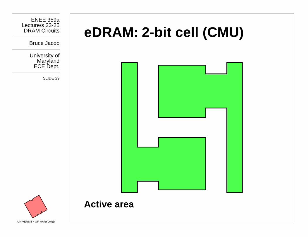
eDRAM: 2-bit cell (CMU)
Active area
ENEE 359aLecture/s 23-25
DRAM Circuits
Bruce Jacob
University ofMaryland
ECE Dept.
SLIDE 30
UNIVERSITY OF MARYLAND
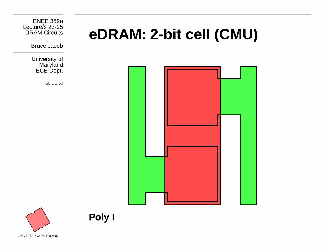
eDRAM: 2-bit cell (CMU)
Poly I
ENEE 359aLecture/s 23-25
DRAM Circuits
Bruce Jacob
University ofMaryland
ECE Dept.
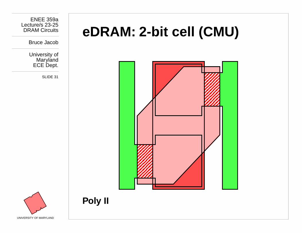
SLIDE 31
UNIVERSITY OF MARYLAND
eDRAM: 2-bit cell (CMU)
Poly II
ENEE 359aLecture/s 23-25
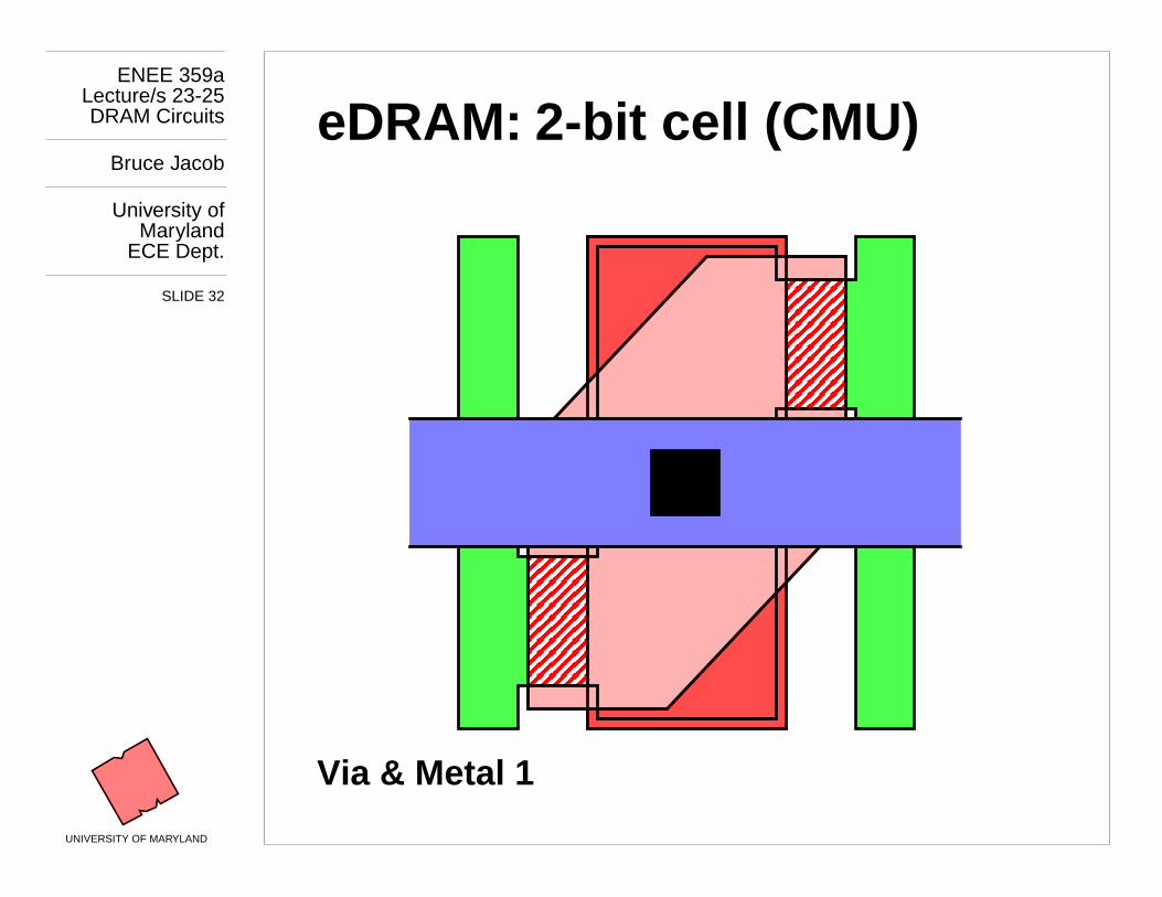
DRAM Circuits
Bruce Jacob
University ofMaryland
ECE Dept.
SLIDE 32
UNIVERSITY OF MARYLAND
eDRAM: 2-bit cell (CMU)
Via & Metal 1
ENEE 359aLecture/s 23-25
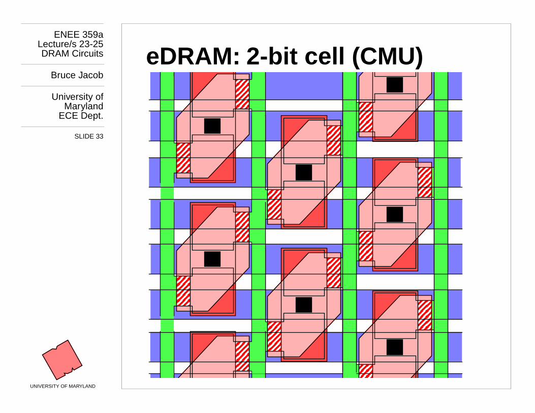
DRAM Circuits
Bruce Jacob
University ofMaryland
ECE Dept.
SLIDE 33
UNIVERSITY OF MARYLAND
eDRAM: 2-bit cell (CMU)