Project 4: Cadence Tools, part 2 (10%)classweb.ece.umd.edu/enee359a.S2007/p4.pdf · 2007-04-12 ·...
13
ENEE 359a: Digital VLSI Design — Project 4: Cadence Tools, part 2 (10%) 1 1. Purpose The objective of this project is to familiarize yourself with the different programs included in Cadence, in particular the physical layout part of VLSI design . The Cadence suite is a huge collection of programs for different CAD applications from VLSI design to high-level DSP programming. The suite is divided into different “packages,” and for VLSI design, the packages we will be using are the IC package and the DSMSE package (we’ll talk about these as we go along). Specifics: After gaining experience with schematic-level transistor design of some basic gates, the next step is to gain some familiarization with how these gates are implemented during the physi- cal layout stage of VLSI design. You will be implementing the inverter, NAND, NOR and MUX gates in a TSMC 0.25um process using the Virtuoso Layout tool. Along the way, you will also perform design rule checks (DRC), layout-versus-schematic checks (LVS), parasitic extraction and SPICE simulation to verify the functionality of your gates. Lastly, similar to project two, you will be doing verification of a pre-designed 10-bit fibonacci counter circuit block. 2. Setup 1. The first thing to do is to setup your directory structure properly so that you can use the required libraries used for the design flow. Download the two files enee359a_files.tar and IIT_stdcells.tar.gz from the Project2 Distribution directory (on course website). 2. In the root of your home directory, extract IIT_stdcells.tar.gz. (First execute ‘gunzip IIT_stdcells.tar.gz’ then untar it by doing ‘tar -xvf IIT_stdcells.tar’) 3. Create your working directory. For the rest of this walkthrough, the assumed name of the working directory will be enee359a. Copy the file enee359a_files.tar to the enee359a directory and untar it there. (Again, do a ‘tar -xvf enee359a_files.tar’). 4. Change any occurrence of the string ‘USERNAME’ in the configuration file ‘cds.lib’ into your user- name and then save as ‘cds.lib’. One way to do this is to use the following: ‘sed ‘s/USER- NAME/your_username/g’ cds.lib.orig > cds.lib’, where you replace “your_username” with your real username. This uses the program sed and redirects its output to the file cds.lib. 3. Inverter design 1. The first step is to create the physical layout of our simplest gate, the inverter. Now, create a ‘layout’ view of your inverter. To do this, in the Lib Manager window, click on simple_cells and then the ‘inv’ cell, then go to File->New->Cellview. Change the tool from Composer-Schematic to Virtuoso. The View Name field should automatically change from schematic to layout. Click on OK. This should open up at least two window -- one titled Virtuoso Layout Editing and another titled LSW. Close any other windows that may have popped-up (mainly text windows informing you what’s new in this version of the tool). 2. Before continuing, familiarize yourself first with the LSW window. This window shows you a list of layers that are available to you to draw shapes on. Most of these layers have physical significance in the sense that they directly control the physical aspects of your layout. For example, click on ‘metal1 - dg’ (this is called a layer-purpose pair in Cadence. It includes a layer name and then the purpose of that layer, which in this case, is a drawing layer, hence the abbreviation ‘dg’. Other purposes can be Project 4: Cadence Tools, part 2 (10%) ENEE 359a: Digital VLSI Design, Spring 2007 Assigned: Thursday, April 12; Due: Tuesday, April 24
Transcript of Project 4: Cadence Tools, part 2 (10%)classweb.ece.umd.edu/enee359a.S2007/p4.pdf · 2007-04-12 ·...

ENEE 359a: Digital VLSI Design
—
Project 4: Cadence Tools, par t 2 (10%)
1
1. Purpose
The objective of this project is to familiarize yourself with the different programs included inCadence, in particular
the physical layout part of VLSI design
. The Cadence suite is a huge collectionof programs for different CAD applications from VLSI design to high-level DSP programming.The suite is divided into different “packages,” and for VLSI design, the packages we will be usingare the IC package and the DSMSE package (we’ll talk about these as we go along).
Specifics: After gaining experience with schematic-level transistor design of some basic gates, thenext step is to gain some familiarization with how these gates are implemented during the physi-cal layout stage of VLSI design. You will be implementing the inverter, NAND, NOR and MUXgates in a TSMC 0.25um process using the Virtuoso Layout tool. Along the way, you will alsoperform design rule checks (DRC), layout-versus-schematic checks (LVS), parasitic extractionand SPICE simulation to verify the functionality of your gates. Lastly, similar to project two, youwill be doing verification of a pre-designed 10-bit fibonacci counter circuit block.
2. Setup
1. The first thing to do is to setup your directory structure properly so that you can use the required libraries used for the design flow. Download the two files enee359a_files.tar and IIT_stdcells.tar.gz from the Project2 Distribution directory (on course website).
2. In the root of your home directory, extract IIT_stdcells.tar.gz. (First execute ‘gunzip IIT_stdcells.tar.gz’ then untar it by doing ‘tar -xvf IIT_stdcells.tar’)
3. Create your working directory. For the rest of this walkthrough, the assumed name of the working directory will be enee359a. Copy the file enee359a_files.tar to the enee359a directory and untar it there. (Again, do a ‘tar -xvf enee359a_files.tar’).
4. Change any occurrence of the string ‘USERNAME’ in the configuration file ‘cds.lib’ into your user-name and then save as ‘cds.lib’. One way to do this is to use the following: ‘sed ‘s/USER-NAME/your_username/g’ cds.lib.orig > cds.lib’, where you replace “your_username” with your real username. This uses the program sed and redirects its output to the file cds.lib.
3. Inver ter design
1. The first step is to create the physical layout of our simplest gate, the inverter. Now, create a ‘layout’ view of your inverter. To do this, in the Lib Manager window, click on simple_cells and then the ‘inv’ cell, then go to File->New->Cellview. Change the tool from Composer-Schematic to Virtuoso. The View Name field should automatically change from schematic to layout. Click on OK. This should open up at least two window -- one titled Virtuoso Layout Editing and another titled LSW. Close any other windows that may have popped-up (mainly text windows informing you what’s new in this version of the tool).
2. Before continuing, familiarize yourself first with the LSW window. This window shows you a list of layers that are available to you to draw shapes on. Most of these layers have physical significance in the sense that they directly control the physical aspects of your layout. For example, click on ‘metal1 - dg’ (this is called a layer-purpose pair in Cadence. It includes a layer name and then the purpose of that layer, which in this case, is a drawing layer, hence the abbreviation ‘dg’. Other purposes can be
Project 4: Cadence Tools, par t 2 (10%)
ENEE 359a: Digital VLSI Design, Spring 2007Assigned: Thur sday, April 12; Due: Tuesda y, April 24

ENEE 359a: Digital VLSI Design
—
Project 4: Cadence Tools, par t 2 (10%)
2
pin (‘pn’), net (‘nt’) and others, but we will be focusing mostly on the drawing purpose). After click-ing on ‘metal1 - dg’, go to the Virtuoso Layout window. Drawing any shape on this window will cre-ate a shape on the metal1-dg layer. To do this, go to Create->Rectangle (shortcut: ‘r’). Click on any point in the screen to define one corner of the rectangle, then click on another point to finish the rect-angle. You should now be able to see a bluish rectangle. Measure the dimensions of this rectangle by going to Window->Create Ruler (shortcut: ‘k’). Use of the ruler should be straightforward, and you should be able to measure the height and width of the rectangle easily. (Note: The labels shown by the ruler are in microns) This rectangle you have drawn represents a physical artifact in the metal1 layer of the process. This means that if you submit this design to a chip foundry, a metal strip in the lowest level metal layer will be created with roughly the dimensions you’ve measured.
3. Now, try creating a 3um x 3um metal1 rectangle. One way you could do this is to “stretch” the rect-angle you’ve already drawn. Go to Edit->Stretch (shortcut: ‘s’) then point the cursor near one edge of your rectangle and click. By moving the mouse, you can stretch the size of the rectangle to any size you want. Use this in conjunction with the ruler tool to finish the 3um x 3um rectangle. (Note: If your ruler markers start getting cluttered up, you can erase all the rulers you’ve created by going to Window->Clear All Rulers, shortcut: shift-K).
4. Notice from the LSW window that our target fabrication process (TSMC 0.25um) has five metal lay-ers. Different processes have different number of layers, and as processes become more sophisti-cated, the number of metal layers tend to increase to give the chip designers more flexibility in routing their more complicated designs. Try drawing rectangles on the poly-dg, metal2-dg, metal3-dg, metal4-dg and metal5-dg to familiarize yourself with the colors of each layer. Similar to metal1-dg, shapes drawn on these layers will directly correspond to a physical artifact when fabricated.
5. Aside from the Create Rectangle command, different other commands exist to draw shapes in Virtu-oso Layout. One of the most useful of these is the Path command. Make sure that the poly-dg layer is selected in the LSW window, then go to Create->Path (shortcut: ‘p’). Click on any point to define the first point of the path. Move the mouse to see the effect. Click on a second point to define a cor-ner for the path, then click on a third point. To finish the path, just press ‘Enter’. Also, if you make a mistake in creating a point in the path, you can delete the last point you’ve defined by pressing ‘Backspace’. By default, the path command will create a path using the minimum possible width for the layer you’re using. If you want to change this width, press ‘F3’ while the path command is active and the Create Path window should pop up. You can change the value in the Width field to change the width, but the more useful command in this window is the “Change To Layer” command. From the pulldown menu, change poly-dg to metal1-dg. In the Layout window, you should now see a rect-angle at the edge of the path you’re creating. Click once, then click on another point to create a new segment then finish the path by pressing ‘Enter’. Notice that while you started the path on the poly-silicon layer, the last segments of the path are now on the metal1 layer. This is called ‘path stitching’, where Layout automatically creates cells called “vias” that are essentially holes in the layout that connect one layer to another. (Note: Right now, you may only be seeing a rectangle where the via should be. To reveal the internal details of the via, press Shift-f and to revert back to the “black box” representation, press Ctrl-f).
6. Other commands that will be useful are the Edit->Move (shortcut: ‘m’) command, the Edit->Copy (shortcut: ‘c’), the Edit->Delete (shortcut: ‘del’) command and the Edit->Undo (shortcut: ‘u’) com-mand. Also, Cadence uses a mode called “gravity” that snaps the cursor to adjacent objects. This is sometimes useful, but I find it better in general to turn it off. To toggle the Gravity mode, press ‘g’ once. You should see the result in the icfb window. Now, delete every shape you’ve created, along with any rulers left in the design.
7. Let’s now proceed with the actual layout of the inverter. The final result should look similar to that of Figure 1. Drawing all the shapes on all the proper layers to define a single MOSFET is pretty involved and will require a more detailed explanation than what we can give here. Fortunately, we can simply instantiate parameterized layouts of the MOSFETs we are going to use. Go to Create->Instance (shortcut: ‘i’). The Create Instance window should pop up. Click on the Browse button, then locate the layout cellview of the Cell ‘nmos’ in the NCSU_Techlib_tsmc03 library. The Create Instance window should now show you different parameters you can vary for this nmos. Like in the schematic, we will be mostly interested in the width of the transistor (leaving the length to be the minimum allowable). In this case, we want to create a minimum-sized NMOSFET so the default of

ENEE 359a: Digital VLSI Design
—
Project 4: Cadence Tools, par t 2 (10%)
3
Figure 1: Finished la yout of a minim um-siz ed inver ter.

ENEE 359a: Digital VLSI Design
—
Project 4: Cadence Tools, par t 2 (10%)
4
450n should be perfect (notice the grayed-out field informing you of the minimum allowable width). Click on anywhere in the Layout window to create one instance of the transistor, then deactivate the Create Instance command by pressing ‘ESC’.
8. At this point, try inspecting the transistor you’ve created. Notice that it takes the combination of a lot of layers to completely define a single NMOS, along with the connections necessary to interface to it. For now, we will only be interested in these connections, specifically the polysilicon and metal1 connections (the red and blue shapes respectively).
9. As an aside, not all shapes in the nmos cell directly correspond to physical artifacts when fabricated. Instead, a combination of some of these shapes are used to define something else. As an example, the outermost green rectangle, (on the nselect-dg layer) will not produce anything when fabricated. Instead, it is used to signify that this transistor is an NMOS, as opposed to a PMOS. For this project, it is not necessary to gain a complete understanding of how all these layers work, although it would be useful later on.
10. The next step is to create a PMOSFET. Do the same thing you did for the nmos but this time, look for the ‘pmos’ cell. In the Create Instance window, change the Width field from 450n to 900n. Again, we want to make the PMOS width twice that of the NMOS width to compensate for the lower carrier mobility in the channel of the PMOSFET so that the equivalent ON resistance of the PMOS will be equal to that of the NMOS such that their drive strengths will be the same and will result in roughly equal rise and fall times of the output. Instantiate the PMOS above the NMOS you’ve created. With the ruler and move command, align the polysilicon gates (the red shape). Also with the ruler and move command, make sure that the tip of the polysilicon gates are separated by 1.8u.
11. Now, the next step is to create the power and ground rails to which we will connect our transistors. Using the Create rectangle tool, draw a 0.9um x 3.6um metal1 rectangle that is 0.6um away from the metal1 shapes of the corresponding NMOS or PMOS transistor. Refer to the Figure 1 to see how the two supply rails should be placed.
12. The next step is to draw the shapes to connect the transistors properly to each other and to the supply rails. First, use either the Create Rectangle or Create Path to connect the two polysilicon gates together (make sure that the poly-dg layer in the LSW window is active). Next, use the Create Rect-angle to connect the drains of the MOSFETs together using a metal1-dg layer. Lastly, connect the source of the PMOS to the upper supply rail and the source of the NMOS to the lower supply rail (Note that a MOSFET is symmetric and either of its terminals can be used as a source or drain. The distinction will depend on the final connection. So for the PMOS, the terminal connected to vdd is considered as the source and the other terminal as the drain. The same goes for the NMOS, substitut-ing gnd for vdd as the supply rail to connect to)
13. Now, it should be emphasized that MOSFETs are actually four-terminal devices. In addition to the gate, source and drain terminal, we also need to be concerned where the substrate of the transistor is connected. Most often, we want to connect the PMOS substrate (which is n-type) to the highest volt-age in the circuit (most often vdd), and the NMOS substrate (which is p-type) to the lowest voltage (most often in CMOS circuits, gnd). To do this, we need to instantiate additional cells to do the con-nection. Press ‘i’ to bring up the Create Instance window, then locate the symbolic cellview of the ‘NTAP’ cell in the NCSU_Techlib_tmc03 library. These ‘NTAP’ cells are used to connect (or “tap”) the n-type substrate underneath. Add two of these ‘NTAP’ cells on top of the PMOS cells the way it is shown on Figure 1. For the NMOS, locate the layout cellview of the ‘ptap’ cell in the NCSU_Techlib_tsmc03 library. These are used to tap the p-type substrate. Instantiate two of these underneath the NMOS as shown in Figure 1. If you have placed everything correctly, the lower edge of the metal connection of the NTAP should coincide with the lower edge of the upper metal1 sup-ply, and the upper edge of the metal connection of the ptap should coincide with the upper edge of the lower metal1 supply. Before proceeding, note that addition of the NTAP causes the nwell-dg layer (the green layer surrounding the PMOS) not to be a rectangle anymore. This is not a problem with this isolated gate, but we will want to place this gate adjacent to other gates eventually, so we want the abutment to be error-free (to be discussed later in the DRC step). Draw an nwell-dg shape to restore the rectangular shape of the n-well (refer to Figure 1).

ENEE 359a: Digital VLSI Design
—
Project 4: Cadence Tools, par t 2 (10%)
5
14. The next step is to provide easy access to the input and output terminals of the inverter. The easiest way to do this is to instantiate vias to the layers we are interested in. In this case, we want to access the polysilicon through a metal2 layer, along with the metal1 output connection of both transistors. First, we need a via that connects the polysilicon to the next higher layer (in this case, metal1). Press ‘i’ to get the Create Instance window then locate the symbolic cellview of the ‘M1_POLY’ cell in the NCSU_Techlib_tsmc03 library and add an instance near the polysilicon like the way it’s shown in Figure 1 (Note that this via cell is the same cell that is automatically created when doing path stitching between metal1 and polysilicon). We now want to make both the input and output terminals available in metal2. To do this, we need to add vias that go from metal1 to metal2. In the Create Instance window, locate the symbolic cellview of the ‘M2_M1’ cell in the NCSU_Techlib_tsmc03 library and add two instances of the via as shown in Figure 1.
15. The last step is to define the input/output pins that will enable the use of this cell in higher-level designs the same way we defined input and output pins for the transistor-level schematic of our inverter. Make sure that the metal2-dg layer is active in the LSW window then go to Create->Pin (shortcut: ctrl-p). Enable “Display Pin Name”, then click on the Display Pin Name option and set Height to 0.5. In the Terminal Names field, enter “A” (without the quotes) and make sure to select ‘input’ as the I/O type. Go back to the Layout window and create a rectangle directly on top of the M2_M1 via you’ve created (Note that you don’t have to enable the Create Rectangle command to create pins). Do the same thing for the output by entering “Y” in the Terminal Names field, making sure to select ‘output’ as the I/O type, and then drawing a metal2 rectangle on top of the M2_M1 via you’ve created earlier. (Note: After creating the rectangles for the pins, you can place the resulting text label anywhere, but it’s useful to place them near the pin they refer to) Lastly, we need to tell Cadence to connect our supply rails to the global vdd and gnd. To do this, make the metal1-dg layer in the LSW window active, then using the Create Shape Pin window, draw a pin called “vdd!” defined as inputOutput I/O type (without the quote and with the exclamation point) on the upper supply rail. Do the same thing for the lower supply rail by drawing a pin called “gnd!” defined also as inputOutput.
16. If you did everything correctly, you should already have a working physical layout of an inverter. Of course, hoping that you’ve created it correctly doesn’t give us any assurance that it will work. The next step is to perform verification steps to make sure that our inverter does work. First, you need to make sure that all the shapes you’ve defined do not violate so called “process design-rules”. These rules define such things as the minimum allowable width of each shape, the spacing between shapes in the same layer and on different layers and a multitude of other things. Imposing these rules allow the chip foundries to reliably create the circuits we are designing. To perform a DRC check, go to Verify->DRC and then click OK (the defaults are perfectly useable). If you didn’t make a mistake, the icfb window should tell you that no errors were found in this layout. If you want, you can delib-erately create an error either by creating new shapes that violate either width rules (say, a metal1 shape that is less than 450n thick) or spacing rules (say, two metal1 shapes that are less than 450n apart), or you can modify the current shapes in your design to come up with an error. After a DRC with errors, you should see a list of errors in the icfb window explaining what errors were found, and error markers should now be seen in the Layout, as demonstrated in Figure 2, where the lower sup-ply rail was intentionally moved upwards, and the polysilicon connection was stretched to introduce a gap. To get an explanation of the error, go to Verify->Markers->Explain and click on an error marker. A new window should pop up with a short explanation of the error. Clicking on the error marker in the polysilicon gap tells us that polysilicon shapes should have a minimum spacing of 0.45um. If the gap was larger or equal to 0.45um, this wouldn’t be flagged as an error during DRC, but obviously the circuit shouldn’t work anymore since the input A is now only connected to the NMOS instead of being connected to the gate of both transistors. This error will be flagged later on during the LVS check since with this error, the layout doesn’t describe the same circuit as the sche-matic anymore.
17. Fix all the errors if any, and do another DRC check until no errors are present.
18. The next step is to do circuit extraction. At its simplest, this step will take all the shapes in your lay-out and try to deduce where transistors are formed and how they are connected to each other and produce a schematic that we can use to compare to our original. We will go a bit further than this and tell the extraction tool to also extract parasitic capacitances within our circuit to create a more realis-tic description of our circuit. Go to Verify->Extract. Make sure that “flat” is chosen as the Extract

ENEE 359a: Digital VLSI Design
—
Project 4: Cadence Tools, par t 2 (10%)
6
method (this creates a flattened schematic in case you have a hierarchical design), and then click on Set Switches and choose Extract_parasitic_caps. Start extraction by clicking on OK. If everything goes correctly, the icfb window should tell you that no errors were found. Mostly, these errors are caused by improperly formed transistors and such, but since we have instantiated the transistors our-selves, there is minimal chance of an error occurring unless we’ve added extra shapes that will inter-fere with the predefined transistor drawing. After extraction is finished, a new cellview called ‘extracted’ is added to the list of cellviews available for the inverter.
19. The next step is to perform a layout-versus-schematic check (LVS) to verify that all those rectangles in our physical layout actually form the same circuit as that defined in the original schematic. In the Lib Manager Window, open the schematic and extracted cellviews of the inverter. In the Virtuoso Layout window showing the extracted cellview, go to Verify->LVS. The LVS window should appear. In the Create Netlist Schematic column, choose Sel by Cursor and then click on the Virtuoso Sche-matic window containing the inverter schematic. In the Create Netlist Extracted column, choose Sel by Cursor and then click on the Virtuoso Layout window containing the extracted waveform. In the LVS options, enable “Rewiring” and “Terminals”. The LVS window should now look like the one shown in Figure 3, assuming that you used the name ‘inv’ for the cell. Start LVS by clicking on the Run button.
20. If everything goes correctly, a window should pop up that says that the LVS run succeeded. This only means that the LVS algorithm finished, and does not mean that the actual LVS check suc-ceeded. Instead, if the run failed, click on Output and then Log and see what the problem is. The most probable reason for failure is that either the schematic or layout cellview is newer than the extracted cellview. If this is the case, save the schematic cellview, then save the layout cellview and perform another extraction and afterwards, do another save and perform the LVS again.
21. To see whether the circuit passed the LVS check, click on Output. This opens a text window and if the circuit passed the check, it should say somewhere that the “net-lists match”, like the one shown in the left window in Figure 4. The LVS check for the layout where the polysilicon gap is still present (and hence the PMOS is unconnected, is shown in the right window of Figure 4. Note the
Figure 2: Inver ter La yout after a DRC c heck sho wing err or marker s (Err ors were intentionall y intr oduced).

ENEE 359a: Digital VLSI Design
—
Project 4: Cadence Tools, par t 2 (10%)
7
line saying that Net /5 merged with /A, which says that the Net /5, in this case the PMOS gate, should actually be connected to /A).
22. After making sure that your netlists match and it has passed the LVS check, the next step is to gener-ate a new cellview called analog_extracted that will be used for SPICE simulation containing the parasitic capacitances. To generate this new cellview, click on Build Analog in the LVS window. In the window that pops up, make sure that Include All is selected (this makes sure that the parasitics include all those found during extraction and any parasitics that you may have explicitly instanti-ated) The icfb window should tell you when the process is finished.
23. At this point, we have finished with the LVS check and should proceed with the SPICE verification. Close all windows except for icfb and Lib Manager. Open the inverter testbench schematic (inv_test) and invoke Analog Design Environment. Configure everything the same way you did for the first inverter SPICE simulation. Start SPICE and display the waveforms on different axes (like before as shown in Project 2)
24. This SPICE run should produce exactly the same results as before. Now, we have to tell Analog Design Environment that instead of using the circuit netlist in the ‘schematic’ cellview (as we did by default during the first SPICE simulation), it should now use the schematic stored in the ‘analog_extracted’ cellview. To do this, go to Setup->Environment and take a look at the switch view list. This is an ordered list of cellviews that Analog Design Environment uses to locate the netlist of our circuit. Even though there are four cellviews entered before ‘schematic’, since our inverter doesn’t contain any of these cellviews, the ‘schematic’ cellview was used during the first SPICE simulation. Type in ‘analog_extracted’ before ‘schematic’ so that the ‘analog_extracted’ cell-view takes precedence and will be used instead of the schematic cellview. Start the SPICE simula-tion and carefully look at the waveforms of the first run and notice the difference when they are automatically replaced by the waveforms of the present run. You will notice that you observe mini-mal changes between the runs. The first thing this means is that your layout is correct and behaves almost the same as the schematic. The second is that the extra parasitics found during extraction does not alter the inverter’s behavior drastically. To appreciate this, you must realize that the transis-tor definitions in the schematic already contain parameters used to define the capacitances of the transistors (click on a transistor then press ‘q’ to bring up its properties. Notice the parameters for drain and source diffusion area and some others. These are used to compute for such values as source and drain junction and diffusion capacitances and some other values). The main difference is that the schematic transistors assume a certain transistor geometry, and this may correspond to the transistor we’ve drawn in the layout, or may be totally way off if we did things like increasing the
Figure 3: LVS windo w for verifi cation of the in ver ter.

ENEE 359a: Digital VLSI Design
—
Project 4: Cadence Tools, par t 2 (10%)
8
area of the source and/or drain. When the design becomes bigger and bigger, extraction of the para-sitic capacitances will produce more deviations from the schematic mainly because of wire parasitic capacitances that start to be significant. In the small inverter layout for example, no parasitic capaci-tance was extracted for the short metal1 layer connecting the drains of the two transistors together.
4. NAND, NOR layout
1. After creating the inverter layout, do the same thing for the NAND and NOR cells. An example lay-out of both gates is shown in Figure5.
2. Some comments regarding the layout:
•
Make sure that the supply rails are aligned properly so that they can be abutted perfectly (i.e.made adjacent without any spacing). Also make sure that they can be abutted perfectly with theprevious inverter design.
•
Although these cells are functionally working, they are not optimized whatsoever. Notice thatthe outputs of the gates are connected together using a metal2 wire. In making standard cells,use of higher-level interconnects are avoided if it is possible to use lower-level interconnectsinstead. In this case, removing the metal1 connections from the middle terminal of the NMOSnetwork for the NAND and the PMOS network for the NOR will allow the connection of theoutputs using a metal1 wire. But to remove the metal1 shape, the PMOS and/or NMOS transis-tors involved have to be flattened (i.e. broken down into their basic layers). As a result, the wholeprocess is more complicated than is necessary four our purpose.
•
For the NOR gate shown here, the worst case drive strength of the PMOS network is weakerthan that of the NMOS network, unlike the inverter and the NAND gate where the drive streng-
Figure 4: LVS outputs f or tw o diff erent runs. The left windo w sho ws a successful L VS check, while the right windo w sho ws the L VS check for the la yout where the PMOS was intentionall y disconnected.

ENEE 359a: Digital VLSI Design
—
Project 4: Cadence Tools, par t 2 (10%)
9
hts are equal. The reason for this is that the two PMOS transistors (width=900n) are in series,yielding an effective width of 450n, which is equal to that of the worst case NMOS networkeffective width. With the difference in carrier mobility, this means that the NMOS drive strengthis roughly twice as strong, the end effect being the fall times of this gate will be faster than therise times.
3. After creating the layout, perform the necessary DRC, extraction and LVS checks the same way you did for the inverter.
4. After doing the LVS check, repeat the ‘Build Analog’ process to generate the analog_extracted cell-view of the gates. Perform SPICE verification for these gates by following the steps used for the inverter and by using the same testbench you used for the NAND and NOR schematic.
Figure 5: Sample la yout of the NAND and NOR cells.
ENEE 359a: Digital VLSI Design
—
Project 4: Cadence Tools, par t 2 (10%)
10
5. MUX design
1. In the same way we used the inverter, NAND and NOR schematic-level basic gates to come up with the gate-level design of a 2-to-1 multiplexer, we can create the multiplexer layout by instantiating the layouts of the individual gates and connecting them together.
2. Create a layout cellview of the multiplexer. Also open the schematic cellview of your multiplexer to guide you in creating the layout.
3. In the Virtuoso Layout window, instantiate instances of the gates you used in the mux schematic (Create->Instance, shortcut: ‘i’). The upper window in Figure 6 shows a multiplexer schematic using the minimum possible gates (given the choice of inv, nand and nor). The lower window shows a lay-out of these four gates instantiated and abutted together. Again, this layout is far from optimal. The gates can be abutted closer to each other such that their power rails overlap. Try abutting the gates closer to each other and use DRC checks to determine at what point further abutment results in a violation (Hint: abutment here is limited by the minimum spacing between diffusion. When the n-select and/or p-select layers overlap, the diffusion layers of the transistors become too close to each other)
4. In the placed layout, notice that the third gate (a NAND gate) is flipped horizontally to allow the A input to be closer to the inverter output to which it is connected. To do this, make the move com-mand active and in the process of moving the gate, press ‘F3’ and then click on the ‘Sideways’ but-ton.
Figure 6: Minim um-gate sc hematic and unfi nished la yout of the m ultiple xer.

ENEE 359a: Digital VLSI Design
—
Project 4: Cadence Tools, par t 2 (10%)
11
5. Next, finish the necessary connections between the gates either by drawing rectangles directly in the metal layers, or using the path command.. It is okay to be sub-optimal this time. The process of stan-dard cell creation is a pretty involved one, and we will not be discussing the techniques here.
6. After finishing the connections, the next step is to define the pins. Create pins (shortcut: ‘ctrl-p’) for the inputs A, B and SEL and the output Y. Lastly, don’t forget to create the vdd! and gnd! pins the same way you did for the basic gates. Be careful to define the I/O types of each properly and make sure to create the pins in the appropriate metal layer (metal1-dg for vdd! and gnd!, and metal2-dg for everything else). An example of the final layout can be seen in Figure 7.
7. Perform DRC, extraction and LVS-checking the same way you did for the basic gates. After passing these checks, generate the ‘analog_extracted’ cellview for use in SPICE.
8. Do SPICE verification of the multiplexer using the testbench you used before for the schematic ver-ification. Make sure to compare the results when using the ‘schematic’ netlist and the ‘analog_extracted’ netlist when doing the SPICE simulation. The presence of the significant length of wires in the final layout may result in significant wiring parasitic capacitances, resulting in more deviation between the schematic and extracted simulation since no wiring capacitances were taken into account in the schematic.
6. Fibonacci La yout
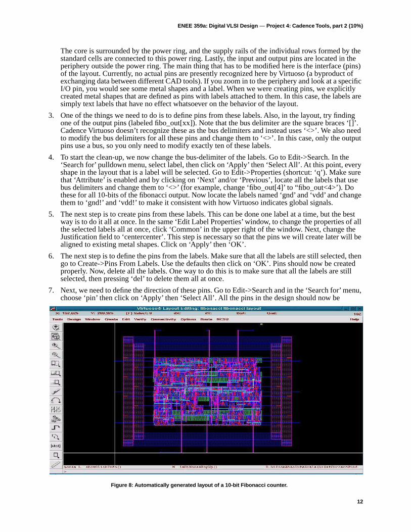
1. So far, most of what we have been doing is creating our own (albeit limited) standard cell library. As previously pointed out, creating a standard cell library is a pretty involved and complicated process. After designing the schematic and layout of the standard cells, the library designer also has to char-acterize the behavior of the standard cell library (in terms of performance, power, area, etc...) and afterwards, make sure that the library is useable on a wide variety of CAD programs from synthesis to PNR (placement and routing) tools. Project 4 will show you a walkthrough of how to complete a reasonably complicated design starting from a high-level HDL design to the final physical layout (verifying the design using DRC, LVS and SPICE along the way). As the last part of Project 3, you will be performing some clean-up of the layout of a10-bit fibonacci counter that was semi-automati-cally generated using the design flow you will use in Project 4.
2. Open the layout cellview of the fibonacci cell. You should see a layout like the one in Figure 8 (again, if you only see the black box view of the cells, press ‘shift-f’ to show everything and ‘ctrl-f’ to go back). Here, the area in the middle that is occupied by the cells is usually called the core area.
Figure 7: Final la yout of the m ultiple xer.
ENEE 359a: Digital VLSI Design
—
Project 4: Cadence Tools, par t 2 (10%)
12
The core is surrounded by the power ring, and the supply rails of the individual rows formed by the standard cells are connected to this power ring. Lastly, the input and output pins are located in the periphery outside the power ring. The main thing that has to be modified here is the interface (pins) of the layout. Currently, no actual pins are presently recognized here by Virtuoso (a byproduct of exchanging data between different CAD tools). If you zoom in to the periphery and look at a specific I/O pin, you would see some metal shapes and a label. When we were creating pins, we explicitly created metal shapes that are defined as pins with labels attached to them. In this case, the labels are simply text labels that have no effect whatsoever on the behavior of the layout.
3. One of the things we need to do is to define pins from these labels. Also, in the layout, try finding one of the output pins (labeled fibo_out[xx]). Note that the bus delimiter are the square braces ‘[]’. Cadence Virtuoso doesn’t recognize these as the bus delimiters and instead uses ‘<>’. We also need to modify the bus delimiters for all these pins and change them to ‘<>’. In this case, only the output pins use a bus, so you only need to modify exactly ten of these labels.
4. To start the clean-up, we now change the bus-delimiter of the labels. Go to Edit->Search. In the ‘Search for’ pulldown menu, select label, then click on ‘Apply’ then ‘Select All’. At this point, every shape in the layout that is a label will be selected. Go to Edit->Properties (shortcut: ‘q’). Make sure that ‘Attribute’ is enabled and by clicking on ‘Next’ and/or ‘Previous’, locate all the labels that use bus delimiters and change them to ‘<>’ (for example, change ‘fibo_out[4]’ to “fibo_out<4>’). Do these for all 10-bits of the fibonacci output. Now locate the labels named ‘gnd’ and ‘vdd’ and change them to ‘gnd!’ and ‘vdd!’ to make it consistent with how Virtuoso indicates global signals.
5. The next step is to create pins from these labels. This can be done one label at a time, but the best way is to do it all at once. In the same ‘Edit Label Properties’ window, to change the properties of all the selected labels all at once, click ‘Common’ in the upper right of the window. Next, change the Justification field to ‘centercenter’. This step is necessary so that the pins we will create later will be aligned to existing metal shapes. Click on ‘Apply’ then ‘OK’.
6. The next step is to define the pins from the labels. Make sure that all the labels are still selected, then go to Create->Pins From Labels. Use the defaults then click on ‘OK’. Pins should now be created properly. Now, delete all the labels. One way to do this is to make sure that all the labels are still selected, then pressing ‘del’ to delete them all at once.
7. Next, we need to define the direction of these pins. Go to Edit->Search and in the ‘Search for’ menu, choose ‘pin’ then click on ‘Apply’ then ‘Select All’. All the pins in the design should now be
Figure 8: Automaticall y generated la yout of a 10-bit Fibonacci counter .

ENEE 359a: Digital VLSI Design
—
Project 4: Cadence Tools, par t 2 (10%)
13
selected. Go to Edit->Properties and in the ‘Connectivity’ section, change the I/O type of the pins one by one (fibo_out<??> should be type output, vdd! and gnd! should be inputOutput, and all other else should be inputs). After finishing, click on OK. (Note: The process is pretty tedious. To make it less tedious, one solution would be to impose a criteria during the selection process such that only common pins are selected. For example, it is possible to select only all the fibonacci outputs so that the properties can be changed all at the same time using the ‘common’ button).
8. At this point, the layout should hopefully be correct. Do a DRC check to verify this. If errors exist, we first need to correct them before proceeding. Go to Verify->Markers->Find. In the window that pops up, enable ‘Zoom to Markers’ and then click on ‘Apply’. This zooms your view to the first error in the circuit and opens up a new window explaining what the error is. Click on ‘Next’ to go the next error if needed. Usually, these types of errors will be caused by some sort of misalignment during the pin-creation step that results in spacing errors between some metal shapes. Move the cre-ated pin to fix the error. From the error markers that are displayed, the source of the error and how to move the pin to fix it should be clear. Do another DRC to verify that all important errors are fixed. Once the layout passes the DRC check, proceed to extraction and LVS checking just like before.
9. After passing the LVS check, generate the ‘analog_extracted’ cellview by clicking on ‘Build Ana-log’ in the LVS window.
10. Redo the SPICE simulation using both the ‘schematic’ cellview and then the ‘analog_extracted’ cellview and compare the outputs.