Brain Inspired Semiconductor Device Technology
29
Exploratory Hybrid Electronic Device Lab. US-KOREA NANO FORUM SEOUL, SEPTEMBER 26, 2016 Byoung Hun Lee Director, Center for Emerging Electronic Materials and Systems (CEEDS) School of Material Science and Engineering, GwangjuInstitute of Science and Technology (GIST) Brain Inspired Semiconductor Device Technology
Transcript of Brain Inspired Semiconductor Device Technology
Exploratory Hybrid Electronic Device Lab.
US-KOREA NANO FORUMSEOUL, SEPTEMBER 26, 2016
Byoung Hun Lee
Director, Center for Emerging Electronic Materials and Systems (CEEDS)
School of Material Science and Engineering,
Gwangju Institute of Science and Technology (GIST)
Brain Inspired Semiconductor Device Technology
Exploratory Hybrid Electronic Device Lab.
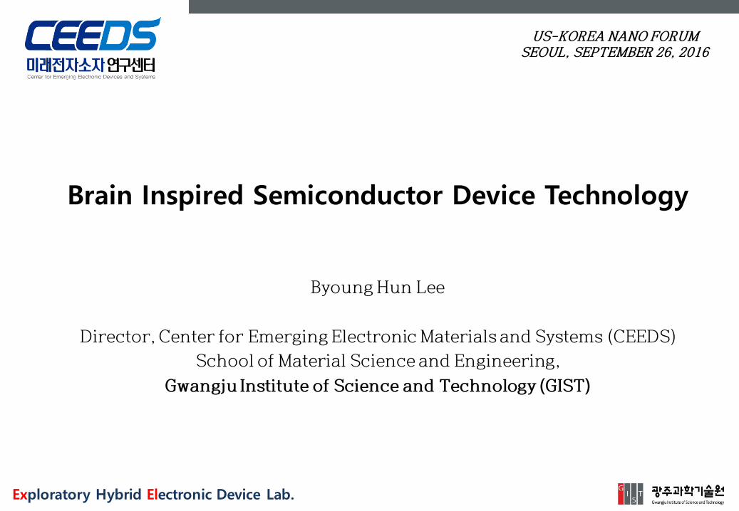
Gwangju Institute of Science and Technology
SCI papers(Papers per faculty / 18 years, 1995-2016)
1st
in the nation
Patents, Research grant 1st
in the nation(Oversea patent application)
QS World University Rankings (Citations per Faculty, 2015/16)
2nd
in the world
THE in 2015 (<50years) 33nd
in the world
KAIST
POSTECH
SNU
GIST

Exploratory Hybrid Electronic Device Lab.
Outline
• Motivation: End of roadmap and energy crisis
• Motivation: Inspirations from brain functions
• Bio inspired semiconductor device technology
• Summary
Exploratory Hybrid Electronic Device Lab.
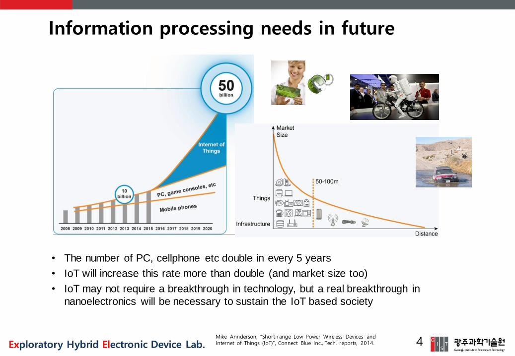
Information processing needs in future
• The number of PC, cellphone etc double in every 5 years
• IoT will increase this rate more than double (and market size too)
• IoT may not require a breakthrough in technology, but a real breakthrough in
nanoelectronics will be necessary to sustain the IoT based society
4Mike Annderson, “Short-range Low Power Wireless Devices and Internet of Things (IoT)”, Connect Blue Inc., Tech. reports, 2014.
Exploratory Hybrid Electronic Device Lab. 5
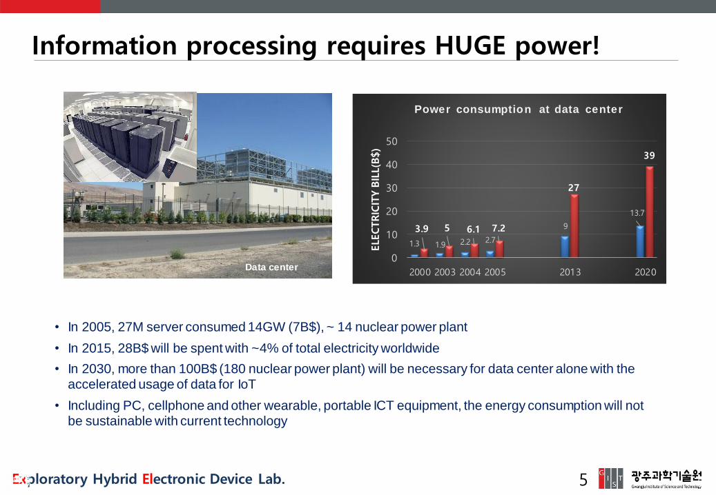
Information processing requires HUGE power!
Data center
• In 2005, 27M server consumed 14GW (7B$), ~ 14 nuclear power plant
• In 2015, 28B$ will be spent with ~4% of total electricity worldwide
• In 2030, more than 100B$ (180 nuclear power plant) will be necessary for data center alone with the accelerated usage of data for IoT
• Including PC, cellphone and other wearable, portable ICT equipment, the energy consumption will not be sustainable with current technology
1.3 1.9 2.2 2.7
9
13.7
3.9 5 6.1 7.2
27
39
0
10
20
30
40
50
2000 2003 2004 2005 2013 2020
ELECTRIC
ITY B
ILL(B
$)
Power consumption at data center
5
Exploratory Hybrid Electronic Device Lab.
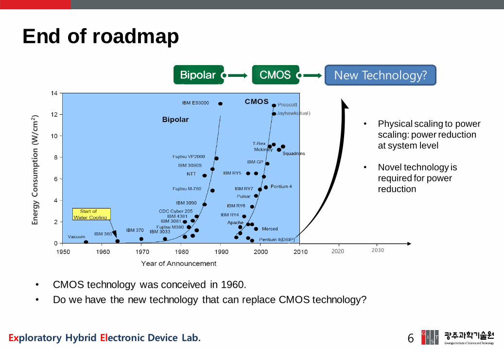
End of roadmap
• CMOS technology was conceived in 1960.
• Do we have the new technology that can replace CMOS technology?
2020 2030
Energ
y C
onsu
mption (W
/cm
2)
New Technology?
• Physical scaling to power scaling: power reduction at system level
• Novel technology is required for power reduction
6
Exploratory Hybrid Electronic Device Lab.Exploratory Hybrid Electronic Device Lab.
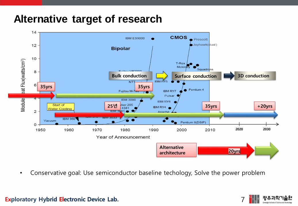
Alternative target of research
7
20yrsAlternative architecture
2020 2030
35yrs35yrs
Bulk conduction
25년 35yrs
Surface conduction 3D conduction
+20yrs
• Conservative goal: Use semiconductor baseline techology, Solve the power problem
Exploratory Hybrid Electronic Device Lab.
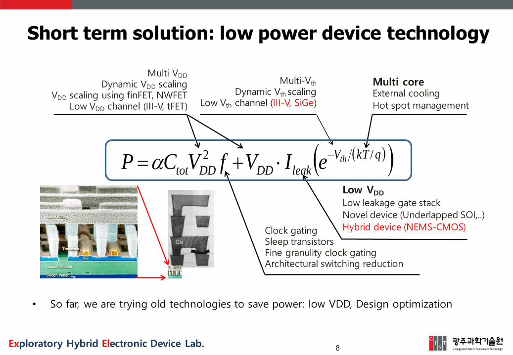
Short term solution: low power device technology
Multi coreExternal cooling
Hot spot management
qkTV
leakDDDDtottheIVfVCP
/2
Multi VDD
Dynamic VDD scalingVDD scaling using finFET, NWFET
Low VDD channel (III-V, tFET)
Clock gatingSleep transistorsFine granulity clock gatingArchitectural switching reduction
Multi-Vth
Dynamic Vth scalingLow Vth channel (III-V, SiGe)
Low VDD
Low leakage gate stack
Novel device (Underlapped SOI,..)
Hybrid device (NEMS-CMOS)
8
• So far, we are trying old technologies to save power: low VDD, Design optimization
Exploratory Hybrid Electronic Device Lab.
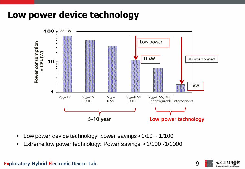
Low power device technology
• Low power device technology: power savings <1/10 ~ 1/100
• Extreme low power technology: Power savings <1/100 -1/1000
9
1
10
100
VDD=1V
Pow
er consu
mption
in C
PU
(W)
VDD=1V3D IC
VDD=0.5V
VDD=0.5V3D IC
VDD=0.5V, 3D ICReconfigurable interconnect
3D interconnect
72.5W
1.8W
Low power
11.4W
5-10 year Low power technology
Exploratory Hybrid Electronic Device Lab.
Summary
1. Problem statement• Future computing/ information processing needs far exceed the capacity of current
energy supply• Key challenge is the total power consumption of system (performance might be a
secondary issue with a parallel and cloud computing route)
2. Origin of problem• Power consumption in a semiconductor chip is reaching its limit• Rack of innovation: scaling for half century (no new device, architecture)
3. Constraints• There is not enough time to fix this problem and get back on track: implementation
of new device and architecture may take more than 20 years easily • Need to solve the problems with existing tools and live with it till full solutions are
available

Exploratory Hybrid Electronic Device Lab.
Outline
• Motivation: End of roadmap and energy crisis
• Motivation: Inspirations from brain functions
• Bio inspired semiconductor device technology
• Summary
Exploratory Hybrid Electronic Device Lab.
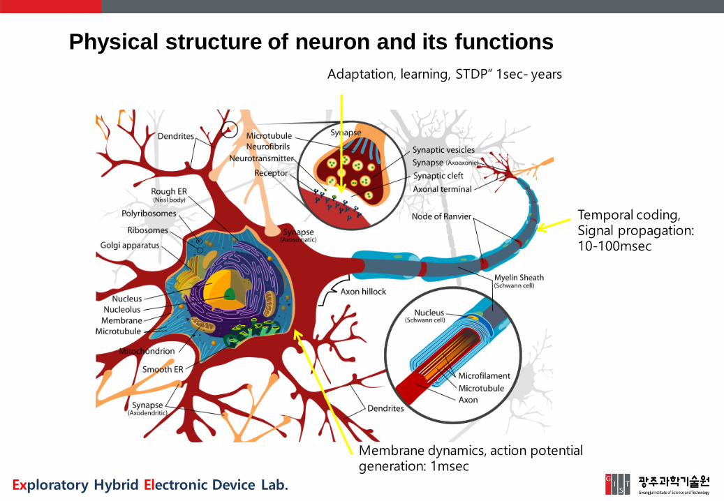
Physical structure of neuron and its functions
Adaptation, learning, STDP” 1sec- years
Temporal coding,Signal propagation: 10-100msec
Membrane dynamics, action potential generation: 1msec
Exploratory Hybrid Electronic Device Lab.
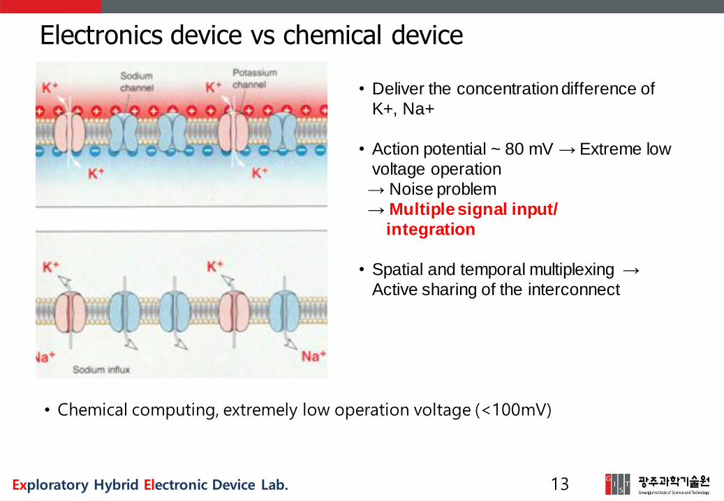
• Deliver the concentration difference of
K+, Na+
• Action potential ~ 80 mV → Extreme low
voltage operation
→ Noise problem
→ Multiple signal input/
integration
• Spatial and temporal multiplexing →
Active sharing of the interconnect
Electronics device vs chemical device
13
• Chemical computing, extremely low operation voltage (<100mV)
Exploratory Hybrid Electronic Device Lab.
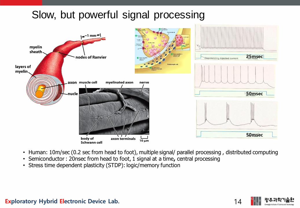
Slow, but powerful signal processing
• Human: 10m/sec (0.2 sec from head to foot), multiple signal/ parallel processing , distributed computing• Semiconductor : 20nsec from head to foot, 1 signal at a time, central processing• Stress time dependent plasticity (STDP): logic/memory function
14
25msec
50msec
50msec
Exploratory Hybrid Electronic Device Lab.
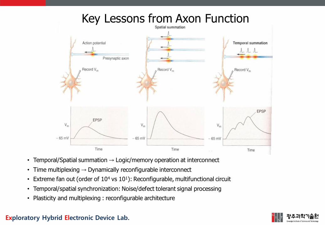
• Temporal/Spatial summation → Logic/memory operation at interconnect
• Time multiplexing → Dynamically reconfigurable interconnect
• Extreme fan out (order of 104 vs 101): Reconfigurable, multifunctional circuit
• Temporal/spatial synchronization: Noise/defect tolerant signal processing
• Plasticity and multiplexing : reconfigurable architecture
Key Lessons from Axon Function
Exploratory Hybrid Electronic Device Lab.
Vertically stacked architecture
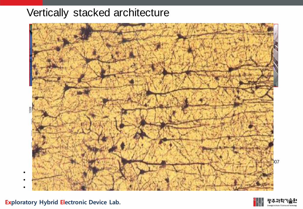
• Brain has roughly 8 device layers while semiconductor has only one
• only 3-4% of devices are operating while 96-97% of ~1B devices are idle
• Reconfigurable architecture
2D FPGA 3D FPGA C. Dong et al., TCS, 2007
New York (8.3M, 105 ppl/km2)
LA (9.8M, 9.3 ppl/km2)
Exploratory Hybrid Electronic Device Lab.
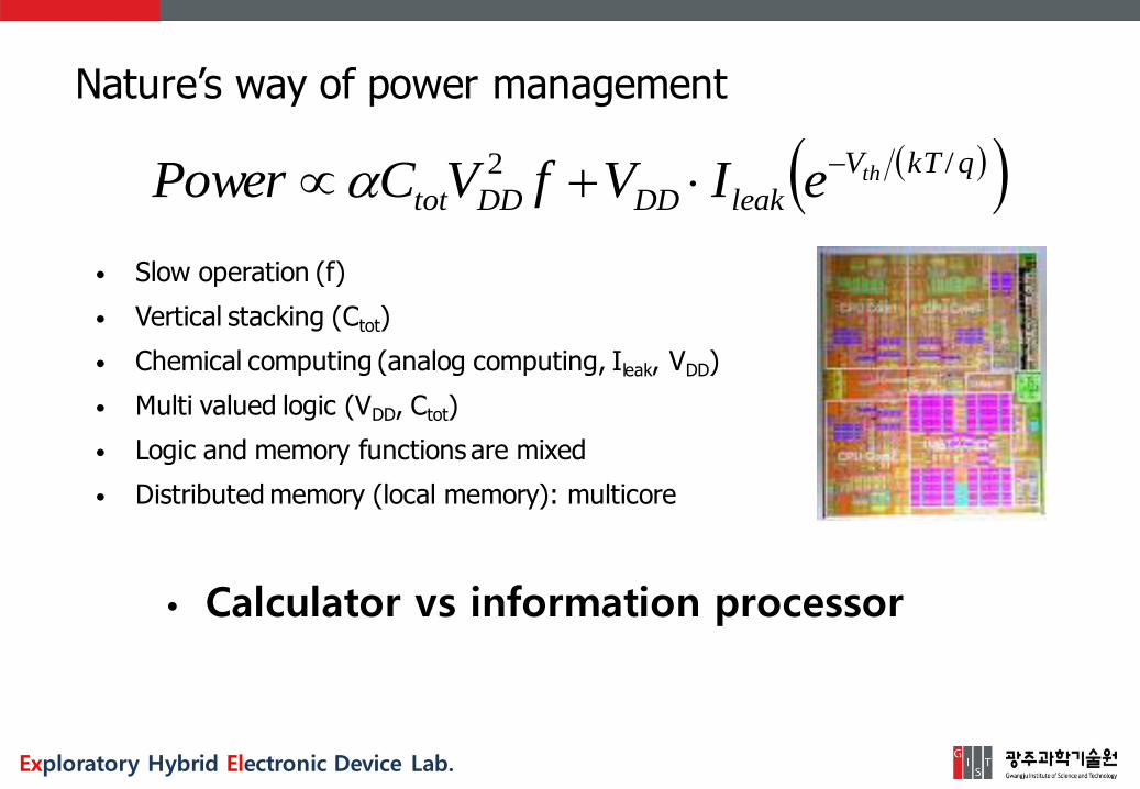
Nature’s way of power management
qkTV
leakDDDDtottheIVfVCPower
/2
• Slow operation (f)
• Vertical stacking (Ctot)
• Chemical computing (analog computing, Ileak, VDD)
• Multi valued logic (VDD, Ctot)
• Logic and memory functions are mixed
• Distributed memory (local memory): multicore
• Calculator vs information processor

Exploratory Hybrid Electronic Device Lab.
Outline
• Motivation: End of roadmap and energy crisis
• Motivation: Inspirations from brain functions
• Bio inspired semiconductor device technology
• Summary
Exploratory Hybrid Electronic Device Lab.
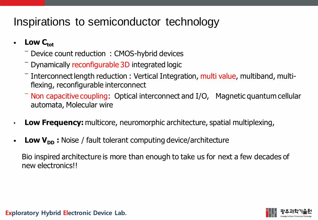
Inspirations to semiconductor technology
• Low Ctot
‾ Device count reduction : CMOS-hybrid devices
‾ Dynamically reconfigurable 3D integrated logic
‾ Interconnect length reduction : Vertical Integration, multi value, multiband, multi-flexing, reconfigurable interconnect
‾ Non capacitive coupling: Optical interconnect and I/O, Magnetic quantum cellular automata, Molecular wire
• Low Frequency: multicore, neuromorphic architecture, spatial multiplexing,
• Low VDD : Noise / fault tolerant computing device/architecture
Bio inspired architecture is more than enough to take us for next a few decades of new electronics!!
Exploratory Hybrid Electronic Device Lab.Exploratory Hybrid Electronic Device Lab.
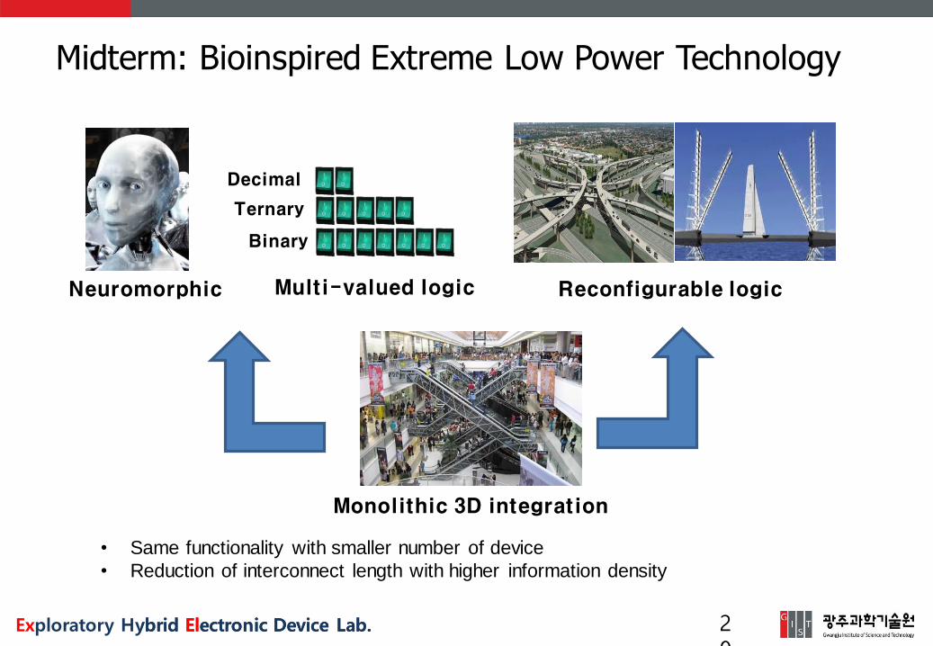
Midterm: Bioinspired Extreme Low Power Technology
Neuromorphic Reconfigurable logic
Decimal
Ternary
Binary
Multi-valued logic
Monolithic 3D integration
• Same functionality with smaller number of device
• Reduction of interconnect length with higher information density
20
Exploratory Hybrid Electronic Device Lab.
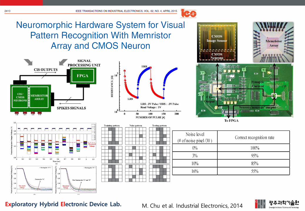
Exploratory Hybrid Electronic Device Lab. M. Chu et al. Industrial Electronics, 2014
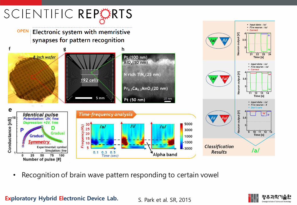
Exploratory Hybrid Electronic Device Lab.
• Recognition of brain wave pattern responding to certain vowel
S. Park et al. SR, 2015
Exploratory Hybrid Electronic Device Lab.Exploratory Hybrid Electronic Device Lab.
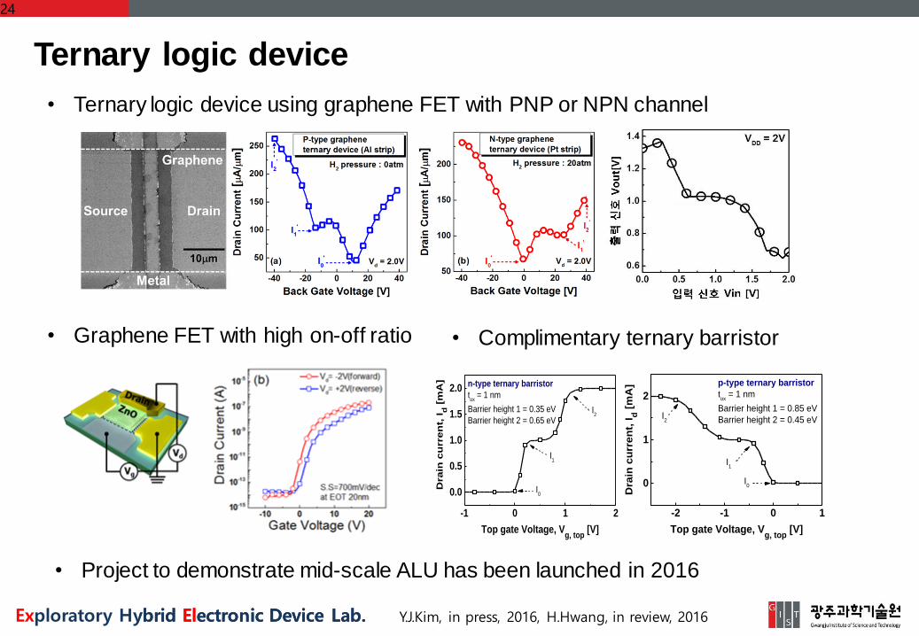
Ternary logic device
24
• Ternary logic device using graphene FET with PNP or NPN channel
• Graphene FET with high on-off ratio
Y.J.Kim, in press, 2016, H.Hwang, in review, 2016
-1 0 1 2
0.0
0.5
1.0
1.5
2.0 n-type ternary barristor
tox
= 1 nm
Barrier height 1 = 0.35 eV
Barrier height 2 = 0.65 eV
I1
Dra
in c
urr
en
t, I
d [
mA
]
Top gate Voltage, Vg, top
[V]
I2
I0
-2 -1 0 1
0
1
2
p-type ternary barristor
tox
= 1 nm
Barrier height 1 = 0.85 eV
Barrier height 2 = 0.45 eV
Dra
in c
urr
en
t, I
d [
mA
]
Top gate Voltage, Vg, top
[V]
I1
I2
I0
• Complimentary ternary barristor
• Project to demonstrate mid-scale ALU has been launched in 2016
Exploratory Hybrid Electronic Device Lab.Exploratory Hybrid Electronic Device Lab.
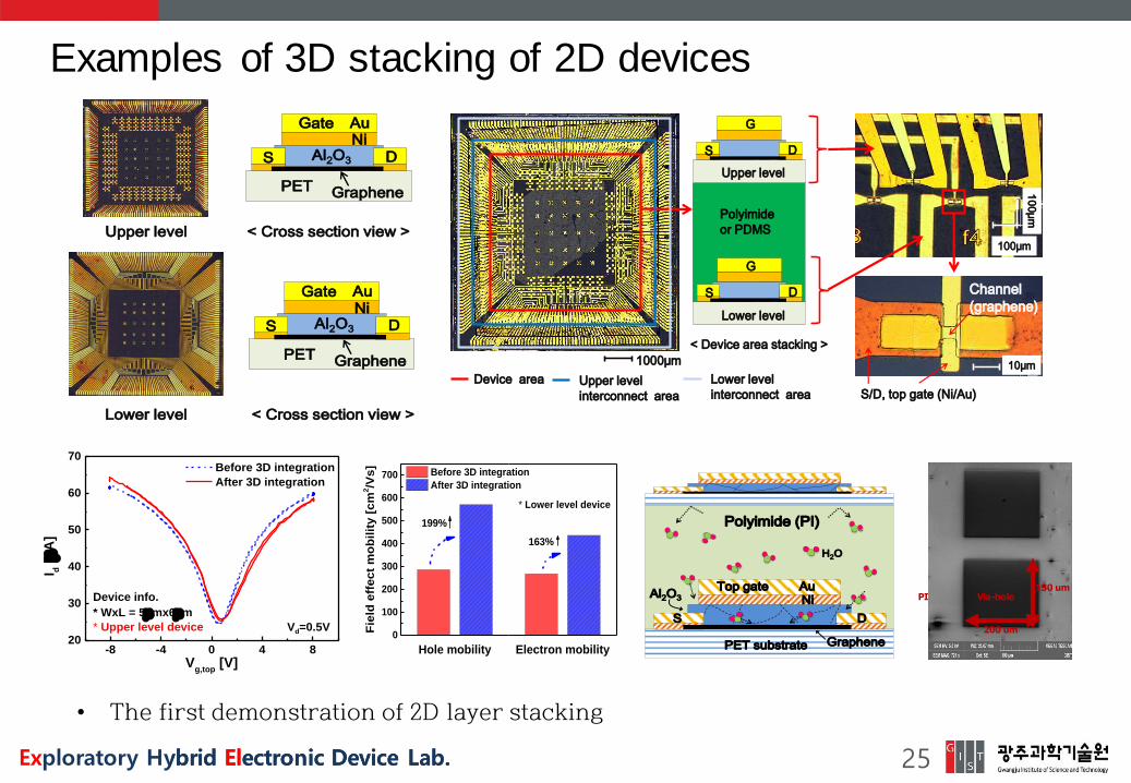
Examples of 3D stacking of 2D devices
Upper level
Lower level
PET
Gate
S D
AuNi
Al2O3
Graphene
PET
Gate
S D
AuNi
Al2O3
Graphene
< Cross section view >
< Cross section view >
1000μm
100μm
10
0μm
10μm
S/D, top gate (Ni/Au)
Channel
(graphene)
G
S D
G
S D
Polyimide
or PDMS
Upper level
Lower level
Device area Upper level
interconnect area
Lower level
interconnect area
< Device area stacking >
-8 -4 0 4 820
30
40
50
60
70
I d [
A]
Vg,top
[V]
Before 3D integration
After 3D integration
Device info.
* WxL = 5mx6m
* Upper level device Vd=0.5V0
100
200
300
400
500
600
700
163%
Before 3D integration
After 3D integration
Fie
ld e
ffect
mo
bilit
y [
cm
2/V
s]
Hole mobility
199%
* Lower level device
Electron mobility PET substrate
S D
Graphene
Al2O3
AuNi
Top gate
H2O
Polyimide (PI)
• The first demonstration of 2D layer stacking
25
150 um
200 um
PI Via-hole
Exploratory Hybrid Electronic Device Lab.
Outline
• Motivation: End of roadmap and energy crisis
• Motivation: Inspirations from brain functions
• Bio inspired semiconductor device technology
• Summary

Exploratory Hybrid Electronic Device Lab.
Summary
• New approach to adapt the novel devices into silicon fab is proposed
• Principles inspired by brain functions will be applied to minimize the power
consumption of silicon chip
• To minimize the performance loss, new technology is better to be used in
BEOL structure with a goal of ;
– Simple circuit
– Low leakage path
– Shorter information travel
– Replace some of FEOL block with power efficient circuits
• Key elements of this technology are being developed
– Dynamically reconfigurable system
– Ternary logic devices and circuits
– Neuromophic circuit
Exploratory Hybrid Electronic Device Lab. 28
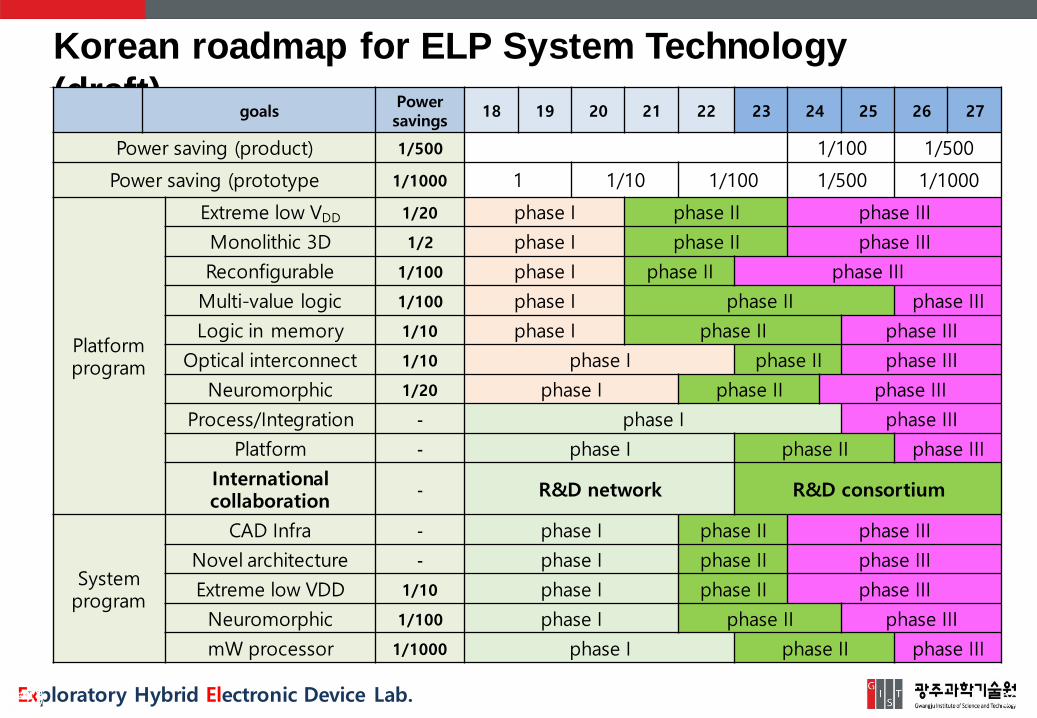
Korean roadmap for ELP System Technology
(draft)goals
Powersavings
18 19 20 21 22 23 24 25 26 27
Power saving (product) 1/500 1/100 1/500
Power saving (prototype 1/1000 1 1/10 1/100 1/500 1/1000
Platform program
Extreme low VDD 1/20 phase I phase II phase III
Monolithic 3D 1/2 phase I phase II phase III
Reconfigurable 1/100 phase I phase II phase III
Multi-value logic 1/100 phase I phase II phase III
Logic in memory 1/10 phase I phase II phase III
Optical interconnect 1/10 phase I phase II phase III
Neuromorphic 1/20 phase I phase II phase III
Process/Integration - phase I phase III
Platform - phase I phase II phase III
International collaboration
- R&D network R&D consortium
Systemprogram
CAD Infra - phase I phase II phase III
Novel architecture - phase I phase II phase III
Extreme low VDD 1/10 phase I phase II phase III
Neuromorphic 1/100 phase I phase II phase III
mW processor 1/1000 phase I phase II phase III

Exploratory Hybrid Electronic Device Lab.