Boson Thermal Imaging Core TM - FLIR are all anticipated in a future field-upgradeable SW release....
118
Copyright 2018 FLIR Systems Inc This datasheet is subject to change without notice Release 300, January 2018 This document is controlled to FLIR Technology Level 2. The information contained in this document pertains to a defense article controlled for export by the International Traffic in Arms Regulations (ITAR). Diversion contrary to US law is prohibited. US Department of State authorization is required prior to export or transfer to foreign persons or parties. Datasheet FLIR Boson TM Thermal Imaging Core General Description Boson TM is a complete thermal imaging core designed to integrate easily into an Original Equipment Manufacturer’s (OEMs) complete system. The core images Long Wave Infrared (LWIR) radiation and outputs a thermal video stream. A highly configurable platform, Boson provides a host of user-selectable features and interfaces for a variety of applications. Features ■ Multiple hardware configurations: ■ QVGA (320x256) and VGA (640x512) sensor array ■ Multiple field-of-view (FOV) options: 8 QVGA FOVs and 8 VGA FOVs ■ Integral shutter assembly ■ Low size, weight, and power (SWAP); capability to trade feature set for power ■ User-configurable I/O with multiple channels for video and command/control, including USB, parallel CMOS, and UART ■ SDIO, I2C, and SPI channels for peripheral support (e.g., memory card, external GPS, gyro, digital compass, etc.); full support to be provided in an upcoming SW upgrade ■ State-of-the-art signal processing, including advanced noise filters for superior sensitivity, eZoom, and colorization ■ Power-safe field upgrade ■ Quick start-up, approx. 2 to 3 sec, depending upon configuration and settings ■ Designed for industrial / military environment ■ RoHS compliant Applications ■ Handheld thermal-imaging systems, such as fire-service, military/paramilitary, and thermography ■ Security & surveillance systems ■ UAV / robotic vision ■ Navigation / obstacle-avoidance ■ Automotive DVE Key Specifications Unless otherwise stated, all specifications apply to all Boson configurations. Imaging Sensor technology Uncooled VOx microbolometer Array format 320x256 or 640x512 Effective frame rate Varies by settings: 60Hz or 30Hz Thermal sensitivity Varies by configuration, as low as <40 mK @ f/1.0 NUC Factory calibrated Field of view 4 o to 95 o HFOV, depending upon lens configuration Electrical Input power 3.3V Power dissipation Varies by configuration, as low as 500 mW Video channels CMOS, BT656-like, or USB2 (see note 1) Control channels UART or USB (see note 1) Peripheral channels I2C, SPI, SDIO (see note 1) Mechanical Size Varies by configuration, as small as 21 x 21 x 11 mm Weight Varies by configuration, as light as 7.5g Environmental Operating temp. -40C to 80C Shock 1500g @ 0.4msec • Note 1: USB3 video, comm via I2C, and I2C, SPI, and SDIO peripheral channels are all anticipated in a future field-upgradeable SW release.
-
Upload
dinhnguyet -
Category
Documents
-
view
215 -
download
2
Transcript of Boson Thermal Imaging Core TM - FLIR are all anticipated in a future field-upgradeable SW release....

Copyright 2018 FLIR Systems Inc This datasheet is subject to change without notice
Release 300, January 2018 This document is controlled to FLIR Technology Level 2. The information contained in this document pertains to a defense article controlled for export by the
International Traffic in Arms Regulations (ITAR). Diversion contrary to US law is prohibited. US Department of State authorization is required prior to export or transfer to foreign persons or parties.
Datasheet
F L I R B o s o n T M T h e r m a l I m a g i n g C o r e
General Description
BosonTM is a complete thermal imaging core
designed to integrate easily into an Original
Equipment Manufacturer’s (OEMs) complete
system. The core images Long Wave Infrared
(LWIR) radiation and outputs a thermal video
stream. A highly configurable platform, Boson
provides a host of user-selectable features and
interfaces for a variety of applications.
Features
■ Multiple hardware configurations:
■ QVGA (320x256) and VGA (640x512) sensor array
■ Multiple field-of-view (FOV) options: 8 QVGA FOVs and 8 VGA FOVs
■ Integral shutter assembly
■ Low size, weight, and power (SWAP); capability to trade feature set for power
■ User-configurable I/O with multiple channels for video and command/control, including USB, parallel CMOS, and UART
■ SDIO, I2C, and SPI channels for peripheral support (e.g., memory card, external GPS, gyro, digital compass, etc.); full support to be provided in an upcoming SW upgrade
■ State-of-the-art signal processing, including advanced noise filters for superior sensitivity, eZoom, and colorization
■ Power-safe field upgrade
■ Quick start-up, approx. 2 to 3 sec, depending upon configuration and settings
■ Designed for industrial / military environment
■ RoHS compliant
Applications
■ Handheld thermal-imaging systems, such as fire-service, military/paramilitary, and thermography
■ Security & surveillance systems ■ UAV / robotic vision
■ Navigation / obstacle-avoidance
■ Automotive DVE
Key Specifications Unless otherwise stated, all specifications apply to all Boson configurations.
Imaging
Sensor technology Uncooled VOx microbolometer
Array format 320x256 or 640x512
Effective frame rate Varies by settings: 60Hz or 30Hz
Thermal sensitivity Varies by configuration, as low as <40 mK @ f/1.0
NUC Factory calibrated
Field of view 4o to 95o HFOV, depending upon lens configuration
Electrical
Input power 3.3V
Power dissipation Varies by configuration, as low as 500 mW
Video channels CMOS, BT656-like, or USB2 (see note 1)
Control channels UART or USB (see note 1)
Peripheral channels I2C, SPI, SDIO (see note 1)
Mechanical
Size Varies by configuration, as small as 21 x 21 x 11 mm
Weight Varies by configuration, as light as 7.5g
Environmental
Operating temp. -40C to 80C
Shock 1500g @ 0.4msec • Note 1: USB3 video, comm via I2C, and I2C, SPI, and SDIO peripheral
channels are all anticipated in a future field-upgradeable SW release.

Boson Thermal Imaging Core
Doc. # 102-2013-40, Release 300
Information on this page is subject to change without notice
2
NOTE: All Specifications are subject to change without notice
Figure 1: Simplified System Block Diagram

Boson Thermal Imaging Core
Doc. # 102-2013-40, Release 300
Information on this page is subject to change without notice
3
Table of Contents 1 DOCUMENT ........................................................................................................................................................... 8
1.1 Revision History ............................................................................................................................................... 8 1.2 Product Upgrade History................................................................................................................................... 8 1.3 Contact Us ......................................................................................................................................................... 8 1.4 Document Conventions ..................................................................................................................................... 9 1.5 Scope ................................................................................................................................................................. 9
2 Key Specifications ................................................................................................................................................. 11 3 System Architecture ............................................................................................................................................... 13 4 Electrical Pinout ..................................................................................................................................................... 15
4.1 Pin Assignments .............................................................................................................................................. 16 4.2 External Circuitry ............................................................................................................................................ 18
5 Signal Pipeline ....................................................................................................................................................... 19
5.1 Frame Averager ............................................................................................................................................... 19 5.2 NUC ................................................................................................................................................................ 20 5.3 Spatial / Temporal Filtering ............................................................................................................................. 22 5.4 AGC ................................................................................................................................................................ 22 5.5 eZoom ............................................................................................................................................................. 23 5.6 Colorize ........................................................................................................................................................... 24 5.7 Symbol Overlay .............................................................................................................................................. 24 5.8 Latency ............................................................................................................................................................ 25
6 Camera Features ..................................................................................................................................................... 26
6.1 Power-On Defaults (User Selectable) ............................................................................................................. 26 6.2 Dynamic-Range Control ................................................................................................................................. 26 6.3 Flat-Field Correction ....................................................................................................................................... 29 6.4 Telemetry ........................................................................................................................................................ 33 6.5 AGC ................................................................................................................................................................ 36
6.5.1 AGC Mode ............................................................................................................................................... 37 6.5.2 Plateau Value ........................................................................................................................................... 37 6.5.3 Tail Rejection ........................................................................................................................................... 38 6.5.4 Max Gain ................................................................................................................................................. 38 6.5.5 Linear Percent .......................................................................................................................................... 39 6.5.6 Adaptive Contrast Enhancement (ACE) .................................................................................................. 39 6.5.7 Digital Detail Enhancement (DDE) ......................................................................................................... 41 6.5.8 Smoothing Factor ..................................................................................................................................... 41 6.5.9 Region of Interest (ROI) .......................................................................................................................... 41 6.5.10 Dampening Factor .................................................................................................................................. 42
6.6 Ezoom ............................................................................................................................................................. 43 6.7 Colorization ..................................................................................................................................................... 46 6.8 Automatic Symbols ......................................................................................................................................... 48 6.9 Customized Symbols ....................................................................................................................................... 51 6.10 Start-up Splash Screen .................................................................................................................................. 54 6.11 Field Calibration ........................................................................................................................................... 56 6.12 Diagnostic Features ....................................................................................................................................... 56
6.12.1 Test Patterns ........................................................................................................................................... 56 6.12.2 Camera Temperature .............................................................................................................................. 57 6.12.3 Status Indicators ..................................................................................................................................... 58
6.13 Upgradeability / Backward Compatibility .................................................................................................... 59

Boson Thermal Imaging Core
Doc. # 102-2013-40, Release 300
Information on this page is subject to change without notice
4
6.13.1 Configuring a Release 2 Camera to Behave Identically to a Release 1 Camera .................................... 60 7 Operating States and Modes .................................................................................................................................. 62
7.1 Start-Up States ................................................................................................................................................ 62 7.2 Overtemp Modes and States............................................................................................................................ 63 7.3 Averager Modes .............................................................................................................................................. 66 7.4 Telemetry Modes ............................................................................................................................................ 66 7.5 Gain Modes and States .................................................................................................................................... 67 7.6 FFC Modes and States .................................................................................................................................... 68
7.6.1 Non-volatile FFC ..................................................................................................................................... 71 7.7 Lens Mode....................................................................................................................................................... 72 7.8 AGC Modes .................................................................................................................................................... 73 7.9 CMOS Video-Tap Modes ............................................................................................................................... 73 7.10 CMOS Color-Encoding Modes ..................................................................................................................... 74 7.11 CMOS Output Modes ................................................................................................................................... 77 7.12 Analog Modes ............................................................................................................................................... 77
8 Interface Descriptions ............................................................................................................................................ 79
8.1 Command and Control Interface ..................................................................................................................... 79 8.2 Video Interfaces .............................................................................................................................................. 83
8.2.1 CMOS ...................................................................................................................................................... 83 8.2.2 USB .......................................................................................................................................................... 89
9 Mechanical Considerations .................................................................................................................................... 90
9.1 Mounting ......................................................................................................................................................... 90 9.2 Sealing ............................................................................................................................................................. 91 9.3 Disassembly .................................................................................................................................................... 92 9.4 Thermal Considerations .................................................................................................................................. 93
10 Optical Characteristics .......................................................................................................................................... 94 11 Image Characteristics ........................................................................................................................................... 96
11.1 Sensitivity...................................................................................................................................................... 96 11.2 Intrascene Temperature ................................................................................................................................. 97 11.3 Operability .................................................................................................................................................... 99
11.3.1 3x3 Cluster Definition .......................................................................................................................... 101 11.3.2 5x5 Cluster Definition .......................................................................................................................... 101
11.4 Image Uniformity ........................................................................................................................................ 101 12 Electrical Specifications ..................................................................................................................................... 105
12.1 DC and Logic Level Specifications ............................................................................................................ 105 12.2 Power Consumption .................................................................................................................................... 105 12.3 Absolute Maximum Ratings ....................................................................................................................... 107
13 Environmental Specifications ............................................................................................................................. 109 14 Compliance with Environmental Directives ....................................................................................................... 110 15 Reliability ........................................................................................................................................................... 110 16 Accessories ........................................................................................................................................................ 110
16.1 USB VPC Kit .............................................................................................................................................. 110 16.2 USB / Analog VPC Kit ............................................................................................................................... 110 16.3 Camera Link Accessory .............................................................................................................................. 112 16.4 Boson Dev Board ........................................................................................................................................ 112 16.5 Tripod-Mount Accessory ............................................................................................................................ 113 16.6 Focus-Tool Accessory ................................................................................................................................. 114
17 References .......................................................................................................................................................... 115
17.1 FLIR Documents ......................................................................................................................................... 115

Boson Thermal Imaging Core
Doc. # 102-2013-40, Release 300
Information on this page is subject to change without notice
5
17.2 External Documents .................................................................................................................................... 115 17.3 Abbreviations / Acronyms .......................................................................................................................... 116
List of Figures
Figure 1: Simplified System Block Diagram ............................................................................................................. 2
Figure 2: Various Configurations of Boson ............................................................................................................. 10
Figure 3: Boson Part-Numbering Schema ............................................................................................................... 10
Figure 4: Boson Simplified Architecture ................................................................................................................. 13
Figure 5: Boson Connector Pin Numbering ............................................................................................................. 15
Figure 6: Recommended USB protection circuitry, to be implemented on interfacing electronics ......................... 18
Figure 7: Boson Signal Pipeline ............................................................................................................................... 19
Figure 8: Boson’s Smart Averager Prevents Blur in Moving Scenes ....................................................................... 20
Figure 9: Example Imagery with Linear and Histogram-based Contrast Enhancement .......................................... 23
Figure 10: Example Imagery Showing eZoom ........................................................................................................ 23
Figure 11: Example Imagery Showing Colorization ............................................................................................... 24
Figure 12: Examples of Boson Symbol Types ......................................................................................................... 24
Figure 13: Example Images, High-Gain State and Low-Gain State ......................................................................... 27
Figure 14: Examples of Good and Grainy Images .................................................................................................... 30
Figure 15: Relative Spatial Noise after FFC vs. Number of Integrated Frames (factory-default = 8) ...................... 32
Figure 16: Example Images Showing Both AGC Modes ......................................................................................... 37
Figure 17: Example Images Showing Three Different Max Gain Values ................................................................ 38
Figure 18: Example Images Showing Different Values of Linear Percent ............................................................... 39
Figure 19: Graphical Illustration of ACE and a corresponding example of the piece wise approximation of the
ACE curve that is implemented. ....................................................................................................................... 40
Figure 20: Example Images Showing Different Values of ACE .............................................................................. 40
Figure 21: Example Images Showing Different Values of DDE .............................................................................. 41
Figure 22: Example Image for 2 Different ROI ........................................................................................................ 42
Figure 23: Visualization of Zoom Function ............................................................................................................. 44
Figure 24: Zoom (Relative Magnification) as a function of specified Zoom Level ................................................ 44
Figure 25: Illustration of “Pan and Tilt”, ................................................................................................................. 45
Figure 26: Boson’s Factory-Loaded Color Palettes .................................................................................................. 46
Figure 27: Sample Image1 With Boson’s Color Palettes .......................................................................................... 47
Figure 28: Sample Image2 with Boson’s Color Palettes .......................................................................................... 47
Figure 29: “FFC Imminent / In Progress” Symbol (Factory-Default) ...................................................................... 48
Figure 30: “FFC Desired” Symbol (Factory-Default) .............................................................................................. 49
Figure 31: “Table-Switch Desired” Symbol (Factory-Default) ................................................................................ 49
Figure 32: “Low-Gain” Symbol (Factory-Default) ................................................................................................... 50
Figure 33: “Overtemp” Symbol (Factory-Default) .................................................................................................. 50
Figure 34: Examples of Boson Symbol Types ......................................................................................................... 52
Figure 35: Examples of Overlapping Symbols, Illustrating Transparency and Z-Location .................................... 54
Figure 36: Example splash-screens, 320x256 and 640x512 resolution ................................................................... 55

Boson Thermal Imaging Core
Doc. # 102-2013-40, Release 300
Information on this page is subject to change without notice
6
Figure 37: Two of the Boson test patterns (shown in both White-Hot and Rainbow palettes) ................................. 57
Figure 38: Boson Start-Up States ............................................................................................................................. 62
Figure 39: Boson Overtemp and Low-power States ................................................................................................ 64
Figure 40: Boson FFC States ................................................................................................................................... 71
Figure 41: Boson Signal Pipeline ............................................................................................................................. 74
Figure 42: Boson’s Various Color-Encoding Modes ................................................................................................ 76
Figure 43: Frame Timing of the CMOS Output Channel ......................................................................................... 84
Figure 44: Line Timing of the CMOS Output Channel ............................................................................................ 85
Figure 45: Phase of Pixel Clock relative to CMOS Data .......................................................................................... 85
Figure 46: Encoding of the CMOS Output Channel for each Video-Tap Mode / Color-Encoding Mode ............... 88
Figure 47: Mounting Guidance for Large-Lens Configurations ............................................................................... 91
Figure 48: Two Camera-Enclosure Options ............................................................................................................. 92
Figure 49: Various Horizontal Fields of View Supported by Boson ........................................................................ 94
Figure 50: Expected NEDT variation over temperature ........................................................................................... 97
Figure 51: Expected maximum scene temperature vs. camera temperature, high-gain state, 320 configuration ..... 98
Figure 52: Expected maximum scene temperature vs. camera temperature, high-gain state, 640 configuration ..... 98
Figure 53: Expected maximum scene temperature vs. camera temperature, low-gain state, 320 configuration ...... 99
Figure 54: Expected maximum scene temperature vs. camera temperature, low-gain state, 640 configuration ...... 99
Figure 55: Examples of 2-pixel clusters.................................................................................................................. 101
Figure 56: Example of Type A INUs ..................................................................................................................... 102
Figure 57: Example of a Type B INU ..................................................................................................................... 102
Figure 58: Example Imagery with and without Supplemental FFC (SFFC) .......................................................... 104
Figure 59: Typical Power Variation of the 320 Release 2 Configuration over Temperature ................................. 106
Figure 60: Typical Power Variation of the 320 Release 1 Configuration over Temperature ................................. 106
Figure 61: Typical Power Variation of the 640 Release 2 Configuration over Temperature ................................. 107
Figure 62: Boson VPC Kit (shown in conjunction with the Boson Tripod Accessory) ......................................... 111
Figure 63: Boson VPC / Analog Kit (shown in conjunction with the Boson Tripod Accessory) ........................... 111
Figure 64: Boson Camera Link accessory .............................................................................................................. 112
Figure 65: Boson Dev Board (with Boson)............................................................................................................. 113
Figure 66: Boson Tripod-mount accessory ............................................................................................................. 113
Figure 67: Boson Focus-tool accessory .................................................................................................................. 114
List of Tables Table 1: Boson Key Specifications ........................................................................................................................... 11
Table 2: Boson Pin Assignments and Pin Description .............................................................................................. 16
Table 3: Assignment of GPIO Pins in Release 1 and Release 2. ............................................................................. 17
Table 4: Telemetry Line Encoding .......................................................................................................................... 33
Table 5: Factory-default attributes of the automatic symbols ................................................................................... 51
Table 6: Camera behavior in each FFC Mode in response to various operating conditions ..................................... 68

Boson Thermal Imaging Core
Doc. # 102-2013-40, Release 300
Information on this page is subject to change without notice
7
Table 7: Partial List of Modes, Parameters, and Operations Controllable through the CCI .................................... 79
Table 8: Timing of the CMOS channel as a function of camera settings, values common to continuous and one-
shot modes ........................................................................................................................................................ 86
Table 9: Timing of the CMOS channel as a function of camera settings, values which differ between continuous
and one-shot modes ........................................................................................................................................... 86
Table 10: Lens Specifications .................................................................................................................................. 95
Table 11: Temporal NEDT in high-gain state .......................................................................................................... 96
Table 12: Operability Requirements by Camera Grade, 320 Configuration .......................................................... 100
Table 13: Operability Requirements by Camera Grade, 640 Configuration .......................................................... 100
Table 14: Allowed Number of INUs by Camera Grade, 320 Configuration ......................................................... 103
Table 15: Allowed Number of INUs by Camera Grade, 640 Configuration ......................................................... 103
Table 16: DC and Logic Levels .............................................................................................................................. 105
Table 17: Absolute Maximum Ratings ................................................................................................................... 107
Table 18: Environmental Specifications ................................................................................................................. 109

Boson Thermal Imaging Core
Doc. # 102-2013-40, Release 300
Information on this page is subject to change without notice
8
1 DOCUMENT
1.1 Revision History
Version Date Comments
Rev 100 October 2016 Initial release
Rev 200 May 2017 Updated to reflect Release 2
Rev 300 Jan. 2018 Updated in reflect Release 2.0.3 for both the 320 and 640 configurations.
1.2 Product Upgrade History The list below lists each Boson software release and a summary of the incremental features/improvements provided by each.
Software Rev #
Release Date Comments
1.0.7405 October 2016 Initial product release (320 configuration only)
2.0.10715 May 2017 Release 2, 320 configuration. Key new features include:
• Symbol overlay
• Splash screen
• Supplemental FFC (SFFC)
• Non-volatile FFC (NVFFC)
• Overtemp protection
• Reduced power
2.0.13705 Jan. 2018 Release 2.0.3: minor bug fixes of the 320 configuration and the initial public release of the 640 configuration.
1.3 Contact Us
In multiple locations throughout this document, FLIR’s Boson website is referenced as a source of additional information. This website can be accessed via the following URL:
http://www.flir.com/cores/content/?id=74595 The website also contains Frequently Asked Questions and a knowledge base:
http://www.flir.com/cvs/cores/knowledgebase/ Additionally, FLIR’s Applications Engineering Department is referenced as a resource for obtaining additional help or information. Email requests can be addressed to [email protected].

Boson Thermal Imaging Core
Doc. # 102-2013-40, Release 300
Information on this page is subject to change without notice
9
1.4 Document Conventions Throughout this document, modes and parameters which are user-configurable via the command and control interface (CCI) are shown in bold font. Status variables which can be read via the CCI (and/or via the telemetry line in some cases) but not directly altered are shown in italic font.
1.5 Scope BosonTM is a highly configurable thermal imaging core comprised of the following 3 major components:
• Lens assembly: Multiple fields of view are available. A lensless configuration is also available with no lens flange. The various lens options are delineated in Section 10.
• Shutter assembly: An integral shutter assembly provides best uniformity by allowing the camera to automatically perform a periodic correction (called flat-field correction) as required.
• Sensor engine: Boson provides both a QVGA (320x256/12 μm) configuration as well as a VGA (640x512/12 μm) configuration. In either case, the focal plane array (FPA) is integrated with common signal-processing electronics, providing state-of-the-art noise filtering, image enhancement, operational logic, and camera functions, as described in Sections 5, 6, and 7. The Boson sensor engine also provides all electrical I/O on a single connector, as detailed in Section 4.
Figure 2 shows some of the available hardware configurations featuring various combinations of lens assembly, shutter assembly, and sensor assemblies. (Not shown are shutterless configurations.) See Section 10 for more information on the available lens configurations.
(a) 320 configurations

Boson Thermal Imaging Core
Doc. # 102-2013-40, Release 300
Information on this page is subject to change without notice
10
(a) 640 configurations
Figure 2: Various Configurations of Boson
Figure 3 shows the part-numbering schema for Boson.
* The last three digits (AA, X) are reserved for customized OEM configurations.
Figure 3: Boson Part-Numbering Schema

Boson Thermal Imaging Core
Doc. # 102-2013-40, Release 300
Information on this page is subject to change without notice
11
2 Key Specifications Unless otherwise stated, all specifications apply to all Boson configurations.
NOTE: As explicitly noted below, some software features are not provided in the current product
release but will be available at a later time via a field-upgradeable software update.
Table 1: Boson Key Specifications
Specification Description
Overview
Sensor technology Uncooled VOx microbolometer
Pixel size 12 μm
Spectral range Longwave infrared, nominally 8 μm to 14 μm
Array format 320x256 or 640x512
Effective frame rate • 60Hz or 30Hz (runtime selectable) • 50Hz or 25Hz (runtime selectable) See note 1
Thermal time constant Nominally 8 msec
Thermal sensitivity Varies by configuration (see Section 11.1 for more detail)
• Industrial grade: < 40 mK • Professional grade: < 50 mK • Consumer grade: < 60 mK
Operability Varies by configuration (see Section 11.3 for more detail)
• Industrial grade: >99%, no clusters > 3x3 • Professional grade: >98.5%, no clusters > 3x3 • Consumer grade: >98%. no clusters > 5x5 • Non-uniformity corrections (NUC) Shuttered configuration capable of automatic flat-field correction
(FFC); all configurations capable of FLIR’s Silent Shutterless NUC (SSN)TM suite of scene-based NUC algorithms (see Section 6.3)
Electronic zoom 1X to 8X zoom (see Section 6.6)
Image orientation Adjustable (vertical flip and/or horizontal flip) See note 2
Symbol overlay Alpha blending for translucent overlay
Snapshots Full-frame snapshot, SDIO interface to support removable media See note 2
Electrical
Video output channel Two options: (see Section 8.2)
• CMOS • USB2 See note 3

Boson Thermal Imaging Core
Doc. # 102-2013-40, Release 300
Information on this page is subject to change without notice
12
Specification Description
Video output format Three runtime-selectable options (see Section 7.9): • Data before AGC (16b, output resolution = sensor
resolution) • Data after AGC, before digital zoom (8b, output resolution
= sensor resolution) • Data after colorization (various bit-width, output resolution
= 640x512 regardless of sensor resolution)
Input clock None required
Frame sync Two runtime-selectable options: • Free-running: Frame timing internally synchronized • Slave mode: Frame timing externally synchronized See note 2
Command & Control Interface (CCI) Three options: (see Section 8.1)
• UART • USB • I2C See note 2
Command & Control API See Boson Software Interface Description Document (IDD)
Peripheral Interfaces • SPI (Boson as master, peripheral as slave device) See note 2 • I2C (Boson as master, peripheral as slave device) See note 2 • SDIO See note 2
Input supply voltage (nominal) 3.3V (See Section 12.1)
Power dissipation Between 500 mW and 1550 mW, configuration and temperature dependent (See Section 12.2)
Mechanical
Package dimensions, lens-less and shutter-less configuration
320 and 640 sensor engine: 21 mm x 21 mm x 11 mm (w x h x d) Note: dimensioned drawings for each Boson configuration are not included herein but are available on the FLIR website. STEP files available upon request. (See Section 1.3)
Weight Varies by configuration, a low as 7.5g. (See Section 10)
Environmental (see Section 13)
Operating temperature range
-40 °C to +80 °C
Storage temperature range -50 °C to +105 °C
Shock 1500 G @ 0.4 ms
ESD EN 61000-4-2 Level 4
Note 1: 50Hz / 25Hz is available only with the CMOS channel configured for BT.656-like output and is
only intended for interface to a display. See Section 7.12.
Note 2: Feature is not provided in the current product release but is anticipated at a later time via field-
upgradable software revision.
Note 3: USB3 is anticipated at a later time via field-upgradeable software revision.

Boson Thermal Imaging Core
Doc. # 102-2013-40, Release 300
Information on this page is subject to change without notice
13
3 System Architecture A simplified architectural diagram of the Boson thermal imaging core is shown in Figure 4.
Figure 4: Boson Simplified Architecture
The lens assembly focuses infrared radiation from the scene through the shutter aperture onto the
sensor engine. The shutter assembly periodically blocks radiation from the scene, presenting a uniform
thermal signal to the sensor array. This uniform input signal allows internal correction terms to be
updated, improving image quality. For applications in which there is little to no movement of the
Boson core relative to the scene (for example, fixed-mount security applications), the shutter assembly
is highly recommended. For applications in which there is ample scene movement (for example,
handheld applications), the shutter is less essential due to FLIR’s Silent Shutterless NUC (SSN)TM
technology, further described in Section 5.3. That said, the shutter is capable of improving image
quality in all applications and is always highly recommended, especially at start-up.

Boson Thermal Imaging Core
Doc. # 102-2013-40, Release 300
Information on this page is subject to change without notice
14
The sensor engine consists of a focal plane array (FPA) integrated with a System on a Chip (SoC). The
FPA is a two-dimensional array of vanadium-oxide (VOx) microbolometers with 12-micron pitch. The
QVGA configuration provides 320x256 pixels while the VGA configuration provides 640x512. The
temperature of each microbolometer varies in response to incident flux. The temperature change
causes a proportional change in the detector’s resistance. VOx provides a high temperature coefficient
of resistance (TCR) and low 1/f noise, resulting in excellent thermal sensitivity and highly stable
uniformity. The microbolometer array is grown monolithically on top of a readout integrated circuit
(ROIC). Once per frame, the ROIC senses the resistance of each detector by applying a bias one row at
a time. The resulting signal is digitized and processed by the SoC, which provides signal conditioning
and output formatting. The SoC is also responsible for all camera logic as well as the Command and
Control Interface (CCI). The signal pipeline is fully defined in Section 5 while the output interfaces are
defined in Section 8.

Boson Thermal Imaging Core
Doc. # 102-2013-40, Release 300
Information on this page is subject to change without notice
15
4 Electrical Pinout As shown in Figure 5, electrical interface to the Boson core is via a single 80-pin connector, Hirose DF40C-80DP-0.4V(51). The recommended mating connector is Hirose 80-pin board-to-board receptacle (socket) DF40HC-(4.0)-80DS-0.4V(51), for a mating stack height of 4.0 mm. Note that the correct orientation of the camera is as depicted in this figure. Rotating the camera 180 degrees such that the connector is below centerline rather than above will result in an upside-down image.
Figure 5: Boson Connector Pin Numbering

Boson Thermal Imaging Core
Doc. # 102-2013-40, Release 300
Information on this page is subject to change without notice
16
4.1 Pin Assignments Pin assignments and description for the Boson main connector are shown in Table 2 and Table 3. Any channels or signals which will not be used should be left floating.
Table 2: Boson Pin Assignments and Pin Description
Pin #
Pin Name
Signal
Type
Signal Level
Description
1, 3, 5, 7, 10, 13, 19, 20, 29, 30, 39, 40, 49, 50, 59, 60, 69, 70, 79
DGND Power GND Digital Ground
2, 4, 6, 8 3V3 Power 3.3V Input Power
11 USB_D_P Diff Pair USB spec compliant USB2 data+
9 USB_D_N Diff Pair USB spec compliant USB2 data-
15 USB_VBUS Power USB spec compliant USB VBus (sense line only, not used to power the Boson core)
17 USB_ID I/O USB spec compliant USB ID
14 USB_TX_P Diff Pair USB spec compliant Reserved for USB3 transmit+ (See note 1)
12 USB_TX_N Diff Pair USB spec compliant Reserved for USB3 transmit-
18 USB_RX_P Diff Pair USB spec compliant Reserved for USB3 receive+
16 USB_RX_N Diff Pair USB spec compliant Reserved for USB3 receive-
21, 22, 23, 25, 26, 27, 28, 31, 32, 33, 34, 35, 36, 37, 38, 41, 42, 43, 44, 45, 46, 47, 48, 51, 52, 53, 54, 55, 56, 57, 58, 61, 62, 63, 64, 65, 66, 67, 68, 71, 73, 74, 75, 76, 77, 78
GPIO I/O 1.8V See Table 3
24 RESET I/O 1.8V (asserted low) See Section 7.1
72 EXT_SYNC I/O 1.8V Reserved for external sync (See note 1)
80 No Connect n/a
Note 1: USB3 and external sync capability are both anticipated via a future field-upgradeable software release.

Boson Thermal Imaging Core
Doc. # 102-2013-40, Release 300
Information on this page is subject to change without notice
17
Table 3: Assignment of GPIO Pins in Release 1 and Release 2.
The discrete I/O pins, I2C channel, SD channel, and SPI channel are not used in Boson Release 1 or Release 2 but are anticipated features of a future field-programmable software upgrade.
Connector pin Signal Name Signal Description
23 GPIO Discrete I/O pin 0
26 GPIO Discrete I/O pin 1
33 uart_apb_sin UART input
43 uart_apb_sout UART output
41 cmos_data_13 CMOS bit13
21 cmos_data_14 CMOS bit14
38 cmos_data_15 CMOS bit15
34 cmos_data_16 CMOS bit16
22 cmos_data_17 CMOS bit17
42 cmos_data_18 CMOS bit18
37 cmos_data_19 CMOS bit19
52 cmos_data_20 CMOS bit20
54 cmos_data_21 CMOS bit21
35 cmos_data_22 CMOS bit22
36 cmos_data_23 CMOS bit23
58 GPIO Discrete I/O pin 2
44 GPIO Discrete I/O pin 3
51 cmos_data_2 CMOS bit2
56 cmos_data_3 CMOS bit3
27 cmos_data_4 CMOS bit4
28 cmos_data_5 CMOS bit5
32 cmos_data_6 CMOS bit6
31 cmos_data_7 CMOS bit7
25 cmos_data_8 CMOS bit8
46 cmos_data_9 CMOS bit9
45 cmos_data_10 CMOS bit10
48 cmos_data_11 CMOS bit11
47 cmos_data_12 CMOS bit12
55 cmos_pclk CMOS pixel clk
53 cmos_vsync CMOS vsync
73 cmos_hsync CMOS hsync
78 cmos_data_valid CMOS data valid
77 cmos_data_0 CMOS bit0
62 cmos_data_1 CMOS bit1
63 i2c_scl I2C Clk
67 i2c_sda I2C Data
75 sd_clk SD clk
66 sd_cmd SD command/response
65 sd_dat_0 SD data0
68 sd_dat_1 SD data1
61 sd_dat_2 SD data2
64 sd_dat_3 SD data3
57 spi_mosi SPI master-out slave-in
76 spi_miso SPI master-in slave-out
74 spi_sclk_out SPI clk
71 spi_ss_out_in_1 SPI chip select

Boson Thermal Imaging Core
Doc. # 102-2013-40, Release 300
Information on this page is subject to change without notice
18
4.2 External Circuitry
• FLIR highly recommends implementing the protection circuit for the USB channel shown in Figure 6 on interfacing electronics if the USB channel is utilized.
• External pull-up resistors (4.7Kohm to 10Kohm) are recommended on all I2C signals if the channel is utilized.
• A pull-down resistor (4.7Kohm to 10Kohm) is recommended on the SPI chip select if the SPI channel is utilized.
• A pull-up resistor (4.7Kohm to 10Kohm) is recommended on the uart_apb_sin signal if the UART is utilized.
Figure 6: Recommended USB protection circuitry, to be implemented on interfacing electronics
Boson Thermal Imaging Core
Doc. # 102-2013-40, Release 300
Information on this page is subject to change without notice
19
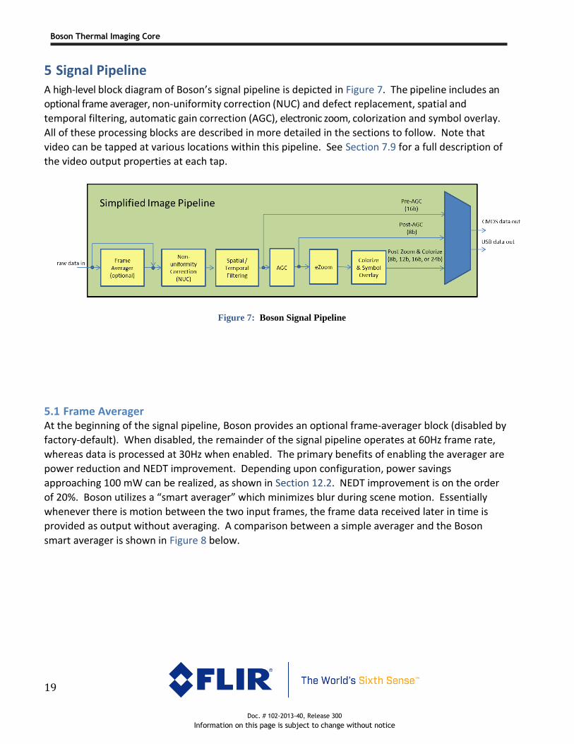
5 Signal Pipeline A high-level block diagram of Boson’s signal pipeline is depicted in Figure 7. The pipeline includes an
optional frame averager, non-uniformity correction (NUC) and defect replacement, spatial and
temporal filtering, automatic gain correction (AGC), electronic zoom, colorization and symbol overlay.
All of these processing blocks are described in more detailed in the sections to follow. Note that
video can be tapped at various locations within this pipeline. See Section 7.9 for a full description of
the video output properties at each tap.
Figure 7: Boson Signal Pipeline
5.1 Frame Averager At the beginning of the signal pipeline, Boson provides an optional frame-averager block (disabled by
factory-default). When disabled, the remainder of the signal pipeline operates at 60Hz frame rate,
whereas data is processed at 30Hz when enabled. The primary benefits of enabling the averager are
power reduction and NEDT improvement. Depending upon configuration, power savings
approaching 100 mW can be realized, as shown in Section 12.2. NEDT improvement is on the order
of 20%. Boson utilizes a “smart averager” which minimizes blur during scene motion. Essentially
whenever there is motion between the two input frames, the frame data received later in time is
provided as output without averaging. A comparison between a simple averager and the Boson
smart averager is shown in Figure 8 below.

Boson Thermal Imaging Core
Doc. # 102-2013-40, Release 300
Information on this page is subject to change without notice
20
Figure 8: Boson’s Smart Averager Prevents Blur in Moving Scenes
NOTE: By factory-default, the frame averager is disabled. Intended use case is that the averager
is enabled once at start-up and optionally saved as a power-on default. Toggling the averager off
and on more than once per power cycle is not recommended and may result in video instability.
5.2 NUC The non-uniformity correction (NUC) block applies correction terms to ensure a uniform output from
each pixel when the camera is imaging a uniform thermal scene such as a blackbody plate. Factory-
calibrated NUC terms are applied to compensate for temperature effects, pixel response variations,
lens-illumination roll-off, and out-of-field irradiance. These terms are enabled by factory default, and
most users will have no reason to ever disable them except as noted below.
• FFC: Unlike all the other corrections applied by the NUC block, FFC is not one-time calibrated but is
instead updated periodically at runtime via a process called flat-field correction (FFC). The FFC
process is further described in Section 6.3.
• Temp-correction: a correction term which compensates for pixel-to-pixel offset variation over
operating temperature
• Gain: a correction term which compensates for pixel-to-pixel responsivity variation. This term is
actually the product of two components, one which compensates for variations stemming from the
sensor assembly and another which compensates for variations stemming from the lens assembly.
On lens-less configurations of Boson or when the Boson camera is installed behind another optical
component, the latter component of the gain term (referred to as the lens-gain map) should be field
calibrated by the user, as described in Section 6.11.

Boson Thermal Imaging Core
Doc. # 102-2013-40, Release 300
Information on this page is subject to change without notice
21
• SFFC: a correction term which compensates for out-of-field irradiance (i.e., the heat radiating from
surfaces inside the camera assembly). If Boson is installed in an enclosure or environment which
significantly increases or reduces camera self-heating, it is recommended that SFFC be field-
calibrated by the user, as described in Section 6.11. Note that SFFC should be disabled when
operating in external FFC mode (see Section 7.6) since the FFC process itself corrects for out-of-field
irradiance when performed using an external source.
• Bad pixel replacement (BPR): a correction process whereby pixels identified as defective are
replaced by a value generated from nearest neighbors
All of the above corrections are arranged into three separate constructs:
• NUC Tables: contain the temperature-compensation terms, and the portion of the gain term which
compensates for variations stemming from the sensor assembly. All NUC tables are factory-
calibrated. There are up to 4 NUC tables stored within the camera:
o NUC Table 0: for professional and industrial-grade configurations, NUC Table 0 is calibrated
for low-gain state and spans the full operating temperature range, -40C to 80C. Consumer-
grade configurations do not contain a Table 0.
o NUC Tables 1 -3: NUC Tables 1 through 3 are calibrated for high-gain state, and each spans a
portion of the total operating temperature range. NUC Table 1 is calibrated from
approximately -40C to -20C, NUC Table 2 s calibrated from approximately -20C to 60C, and
NUC Table 3 is calibrated from approximately 60C to 80C. At start-up, Boson automatically
loads and applies the proper table, and if during operation the camera heats or cools down
such that a different table is optimum, the camera switches tables automatically (if in
automatic FFC mode) or signals a Table Switch Desired status if in manual or external FC
mode. See Section 7.6 for a description of FFC modes. See Section 6.12.3 for a description
of the Table Switch Desired Status.
• Lens Tables: the lens tables are comprised of the portion of the gain term stemming from the
lens assembly, the SFFC correction, and (if field-calibrated), the NVFFC. At start-up, Boson
automatically loads whichever lens table is stored as the power-on default (Lens 0 or Lens 1).
The switch from one lens table to another is only via user-command. Boson configurations
which include a lens are shipped with factory-calibrated lens-gain and SFFC correction terms in
Lens 0, while Lens 1 is empty. As described in Section 6.11, it may be beneficial to replace the
factory calibration with a field calibration, depending upon installation conditions. Lens-less
configurations are shipped with both Lens 0 and Lens 1 empty, and it is necessary to perform a
field calibration once a lens is installed. The decision to calibrate the NVFFC map is application-
dependent, as described in Section 7.6.1.

Boson Thermal Imaging Core
Doc. # 102-2013-40, Release 300
Information on this page is subject to change without notice
22
• Defect Map: there is a single defective-pixel map, which is applied independently of NUC-table
or Lens-table selection. The map is factory calibrated, but the user has the option of adding
pixels to it. (This operation occurs automatically as part of the lens-calibration process described
in Section 6.11.) The user also has the option to restore the factory-calibrated map in the event
that non-defective pixels are inadvertently added during operation.
5.3 Spatial / Temporal Filtering The signal pipeline includes a number of sophisticated image filters designed to enhance signal-to-
noise ratio (SNR) by reducing temporal noise and residual non-uniformity. The filtering suite includes
FLIR’s Silent Shutterless NUC (SSN)TM technology, which is an advanced set of scene-based NUC
algorithms. SSN relies on motion within the scene to isolate fixed pattern noise (FPN), which is then
removed dynamically. The filtering suite also contains algorithms optimized for reduction of row and
column noise. Like the NUC block, the filtering steps performed in this block are transparent to the
user and require no external intervention or support.
Below is a brief description of the various filters which are all enabled by factory default. Most users will
have no reason to ever disable any of them, and generally speaking, temporal noise or uniformity will
degrade as the result of doing so.
• Spatial column noise reduction (SCNR): a filter intended to minimize column noise
• Silent Shutterless NUC (SSN): a filter intended to minimize random spatial noise
• Temporal filter (TF): a filter intended to minimize temporal noise
NOTE: While the spatial filtering algorithms described above are intended to minimize residual
non-uniformity, FLIR always recommends using either Boson’s internal shutter or an external
shutter design to perform periodic FFC for highest image quality.
5.4 AGC Boson provides a highly-configurable contrast-enhancement algorithm for converting 16-bit data to
an 8-bit output suitable for display. Unlike the NUC block and Spatial / Temporal Filtering block, the
AGC block includes a number of user-selectable parameters which allow the image enhancement to
be tailored for application, scene conditions, and subjective taste. See Section 6.5 for a complete
description of the algorithm and all associated parameters.

Boson Thermal Imaging Core
Doc. # 102-2013-40, Release 300
Information on this page is subject to change without notice
23
(a) Linear AGC example. (b) Histogram-based AGC example
Figure 9: Example Imagery with Linear and Histogram-based Contrast Enhancement
5.5 eZoom The electronic zoom block provides an optional interpolation of a subset of the field of view to the
640x512 resolution of the output stream. For example, it is possible to select the central 50% of
the pixel area and stretch it to the full output resolution, resulting in a 2X zoom. See Section 6.6 for
a more complete description of the feature and its associated parameters.
(a) 1X zoom (full FOV displayed) (b) 2X zoom (half FOV displayed)
Figure 10: Example Imagery Showing eZoom

Boson Thermal Imaging Core
Doc. # 102-2013-40, Release 300
Information on this page is subject to change without notice
24
5.6 Colorize The colorize block takes the contrast-enhanced, post-eZoom thermal image as input and generates
an output in which a color palette is applied. Boson provides a number of built-in color palettes,
as described in Section 6.7.
(c) Monochrome Image (d) Colorized Image
Figure 11: Example Imagery Showing Colorization
5.7 Symbol Overlay The symbol-overlay block overlays symbol patterns over the infrared image. In addition to several
automatic symbols described in Section 6.8, the symbol overlay block also allows display of user-
specified symbols, as exemplified in Figure 12. A full description of Boson’s custom-symbol
capabilities is provided in Section 6.9.
Figure 12: Examples of Boson Symbol Types

Boson Thermal Imaging Core
Doc. # 102-2013-40, Release 300
Information on this page is subject to change without notice
25
5.8 Latency Latency of the Boson signal pipeline is defined as the time difference between when the signal level
of a given pixel is read from the sensor and when that signal is available as output from the camera.
Referring to Figure 7, it is the amount of time for “raw data in” to be fully processed to “data out” at
the selected video channel. The value varies depending upon where in the signal chain the output is
tapped, as follows:
• Pre-AGC: ~18 msec
• Post-AGC: ~19 msec (1 msec greater than the pre-AGC tap)
• Post-zoom: ~37 msec (18 msec greater than the post-AGC tap)
For all three tap points, the output channel utilizes a multi-frame buffer as described in Section
7.11. This buffer introduces a frame of latency, which is the dominant latency source for the pre-
AGC and post-AGC taps. For the post-zoom tap-point, the zoom operation itself also utilizes a
multi-frame buffer, introducing a second frame of latency. The remaining fractions of a frame-time
in the latency values provided above are the processing time required by the various blocks in the
signal pipeline.
NOTE: The averager function combines two frames of the data from the sensor. The latency
numbers shown above are applicable to the second of the two frames (the later frame) when the
averager is enabled.
NOTE: Boson’s sensor assembly has a characteristic thermal time constant, nominally 8 msec.
It is not traditional to include time constant in the latency definition.

Boson Thermal Imaging Core
Doc. # 102-2013-40, Release 300
Information on this page is subject to change without notice
26
6 Camera Features Boson provides a number of operating features, more completely defined in the sections which follow.
■ Power-On Defaults, page 26 ■ Dynamic-Range Control, page 26 ■ Flat-field Correction, page 29 ■ Telemetry, page 33 ■ AGC, page 36 ■ E-Zoom, page 43 ■ Colorization, page 46 ■ Symbol Overlay, page 48 ■ Field Calibration, page 56 ■ Diagnostic Features, page 56 ■ Upgradeability / Backward Compatibility, page 59
6.1 Power-On Defaults (User Selectable) Boson provides a “save defaults” capability which allows all current mode and parameter settings to be stored as power-on defaults. Boson also provides the ability to restore the original factory default settings (which can then be re-saved as power-on defaults). See Table 7 in Section 8.1 for a list of affected modes and parameters. The table also shows the factory-default value for each setting.
6.2 Dynamic-Range Control To support a wide range of scene temperatures while providing optimum sensitivity, the industrial and professional grades of Boson provide two gain states: high-gain and low-gain. In high-gain state, the thermal sensitivity is highest (i.e., NEDT is lowest), but hot objects in the scene are prone to saturation. In low-gain state, the thermal sensitivity is lower, but scene range is significantly higher. (See Sections 11.1 and 11.2, respectively, for NEDT and intrascene range in both gain states.) Figure 13 depicts example imagery for both states. In the high-gain example, it is easier to see subtle temperature differences (e.g., the smoke rising from the grill), but the entire surface of the grill is saturated. In the low-gain example, it is possible to resolve thermal details within the hot grill (because the pixels are not saturated), but the subtler temperature differences are harder to discern.

Boson Thermal Imaging Core
Doc. # 102-2013-40, Release 300
Information on this page is subject to change without notice
27
(a) High-gain state
(higher sensitivity, lower scene range)
(b) Low-gain state
(lower sensitivity, higher scene range)
Figure 13: Example Images, High-Gain State and Low-Gain State
NOTE: The consumer grade of Boson does not provide multiple dynamic-range-control modes
and instead always operates in high-gain mode.
There are a number of user-selectable parameters associated with Boson’s dynamic range control
feature, each of which is described below.
■ Gain Mode (high-gain, low-gain, or automatic): determines whether or not Boson
automatically determines the optimum gain state based on current scene conditions. See
Section 7.5 for a detailed description of these modes. Default value is high-gain. None of
the remaining parameters listed below have any effect except when in automatic gain
mode.

Boson Thermal Imaging Core
Doc. # 102-2013-40, Release 300
Information on this page is subject to change without notice
28
■ High-to-Low Intensity Threshold: In conjunction with the parameter High-to-Low
Population, the High-to-Low Intensity Threshold parameter defines the scene conditions
which result in the camera determining that a switch from high-gain state to low-gain
state is desired. (When operating in automatic gain mode and automatic FFC mode, an
automatic switch of gain state takes place when the camera determines it is desired.
When operating in automatic gain mode and manual or external FFC mode, a desired gain
switch is signaled via the Table Switch Desired flag and the Desired NUC Table status
having a value of 0, as described below.) The High-to-Low Intensity Threshold represents
the intensity above which a pixel is scored as being one which would benefit from
transition to low-gain state. It is typically set to a value near high-gain saturation. (The
factory-default value, 90% represents 90% of the maximum output value and is
recommended under most operating conditions.)
■ High-to-Low Population Threshold: In conjunction with the parameter High-to-Low
Intensity Threshold, the High-to-Low Population defines the scene conditions which
result in a desired change from high-gain state to low-gain state. It represents the
percentage of the pixel population which must have intensity exceeding High-to-Low
Intensity Threshold for a desired gain-state change to be signaled. The factory-default
value is 5%. A larger value requires a larger percentage of pixels to be imaging hot
objects to produce that result.
■ Low-to-High Population Threshold: In conjunction with the Hysteresis and High-to-Low
Intensity Threshold parameters, Low-to-High Population Threshold defines the scene
conditions which result in the camera determining that a switch from low-gain state to
high-gain state is desired. The Low-to-High Population Threshold represents the
percentage of the pixel population which must have intensity below the Low-to-High
Intensity Threshold for a desired gain-state change to be signaled. The factory-default
value is 98%. The value cannot be set to less than (100% - High-to-Low Population
Threshold) to prevent scene conditions which might result in oscillation between gain
states.
■ Hysteresis: In conjunction with the High-to-Low Intensity Threshold parameter,
Hysteresis affects the calculated camera variable Low-to-High Intensity Threshold. The
factory-default value of Hysteresis is 95%. The lower the value, the cooler the scene
must be to result in a desired switch back to high-gain state.
In addition to the user-selectable parameters associated with the dynamic-range control feature,
Boson provides three status variables reported via the telemetry line (see Section 6.4) or by status
request on the CCI (see Section 8.1):
■ Current NUC Table: The Current NUC Table variable has a value of 0 when operating in low-
gain state and a value greater than 0 (either 1, 2, or 3) when operating in high-gain state. For
an explanation of NUC Tables, see Section 5.2.

Boson Thermal Imaging Core
Doc. # 102-2013-40, Release 300
Information on this page is subject to change without notice
29
■ Desired NUC Table: The Desired NUC Table variable is automatically set based on ambient
temperature, scene conditions and the selectable parameters described above. When in
automatic gain mode, an automatic NUC table switch takes place whenever the Desired
NUC Table value does not match the value indicated via Current NUC Table. In manual or
external FFC mode, a table switch only occurs in response to “Table Switch” command.
Note that if Current NUC Table = 0, and Desired NUC Table > 0, a NUC table switch
(automatic or commanded) causes the camera to switch from low-gain state to high-gain
state. Conversely, if Current NUC Table > 0, and Desired NUC Table = 0, a table switch
causes the camera to switch from high-gain state to low-gain state. Note that the “Table
Switch” command has no effect when Current NUC Table = Desired NUC Table. That is, no
table switch occurs under that condition.
■ Table Switch Desired: The Table Switch Desired flag is set whenever Desired NUC Table is
not equal to Current NUC Table. When in automatic FFC mode, this flag is never set
because instead an automatic table switch takes place. When in manual or external FFC
mode, commanding a table switch when this flag is set will cause the switch to take place.
(Commanding a table switch when the flag is not set has no effect.) By factory default, a
red circle will appear in a location which circumscribes the FFC Desired symbol whenever
the Table Switch Desired flag is set. (See Figure 31 in Section 6.9.)
6.3 Flat-Field Correction Boson is factory calibrated to produce output imagery which is highly uniform when viewing a
uniform-temperature scene, such as shown in Figure 14a. However, drift over long periods of time can
degrade uniformity, resulting in imagery which appears more grainy (Figure 14b). Operation over a
very wide temperature range (for example, powering on at -20 °C and heating to 60 °C) can also lead
to a grainier image.

Boson Thermal Imaging Core
Doc. # 102-2013-40, Release 300
Information on this page is subject to change without notice
30
(a) Uniform image
(b) Grainy image
Figure 14: Examples of Good and Grainy Images
For scenarios in which there is ample scene movement, such as most handheld applications, Boson is
capable of automatically compensating for drift effects with FLIR’s Silent Shutterless NUC (SSN) suite of
algorithms. However, for use cases in which the scene is essentially stationary, such as fixed-mount
applications, SSN is less effective. In those scenarios, it is recommended to periodically perform a flat-
field correction (FFC). FFC is a process whereby the NUC terms applied by the camera's signal
processing engine are recalibrated to produce optimal image quality. The sensor is briefly exposed to a
uniform thermal scene, and the camera updates the NUC terms to ensure uniform output. The entire
process takes less than a second. As described in Section 7.6, Boson can be configured to perform a
FFC automatically or only upon command via the CCI. Furthermore, Boson can be configured to use
its internal shutter or to use an external scene as the uniform source. In the latter case, the camera
must be viewing the uniform scene before FFC is commanded.
NOTE: If FFC is performed in “External” FFC mode while imaging a non-uniform scene, the
scene will be “burned in” to the correction map, resulting in severe image artifacts.

Boson Thermal Imaging Core
Doc. # 102-2013-40, Release 300
Information on this page is subject to change without notice
31
There are a number of user-selectable parameters associated with the FFC process which control
when FFC events occur. Each is described below.
■ FFC Mode (automatic, manual, or external) determines whether or not Boson performs FFC
automatically and whether or not it uses the internal shutter during an FFC event. See
Section 7.6 for a detailed description of these modes. Factory-default is “automatic”,
which means that FFC events are triggered by:
• Start-up
• Expiration of internal timer with period specified by FFC Period (see below)
• Temperature change beyond FFC Temp Delta (see below)
• Change in NUC table (see Section 5.2)
• Explicit command
■ FFC Integration Period: During each FFC event, the camera automatically integrates n
frames of sensor data to generate the resulting correction term. FFC Integration Period
specifies the value of n, either 2, 4, 8 or 16. Utilizing fewer frames obviously decreases
the FFC period (with diminishing returns due to overhead) whereas utilizing more frames
provides greater reduction of spatial noise (also with diminishing returns due to 1/f noise).
Figure 15 quantifies the benefit. The factory-default value is 8 frames. Note that with
averager enabled (i.e., 30Hz output rather than 60Hz output), a value of 8 frames
represents twice as much time as with averager disabled. That is, for the same value of
FFC Integration Period, the time required to complete FFC is approximately twice as long
with averager enabled.
■ FFC Period: When the camera is in automatic FFC mode, FFC Period defines the
maximum elapsed time between automatic FFC events. When the camera is in manual or
external FFC mode, this parameter defines the maximum elapsed time before the FFC
Desired flag is enabled. (See below.) FFC Period is specified in seconds (e.g., the factory-
default value of 900 represents a 900 second (15 minute) maximum time between
successive FFC events). A specified value of 0 is an exception which disables the time-
based trigger. The factory-default value is recommended under most operating
conditions.
■ FFC Temp Delta: When the camera is in automatic FFC mode, FFC Temp Delta defines
the maximum temperature change of the FPA between automatic FFC events. When the
camera is in manual or external FFC mode, this parameter defines the temperature
change which triggers the FFC Desired flag to be set. FFC Temp Delta is specified in
tenths of a Celsius degree (e.g., the factory-default value of 30 represents a 3 deg temp
change between successive FFC events). A specified value of 0 is an exception which
disables the temp-based trigger. The factory-default value is recommended under most
operating conditions.

Boson Thermal Imaging Core
Doc. # 102-2013-40, Release 300
Information on this page is subject to change without notice
32
■ FFC Start-up Period: When Boson is first powered, it experiences rapid self-heating in the
first few minutes of operation. During this time, it benefits from more frequent FFC
events than required during steady-state operation. FFC Start-up Period specifies a
period of time (in seconds) after power-up during which the camera triggers FFC in
response to temperature change equal to one-third of the value of FFC Temp Delta. For
example, if FFC Temp Delta is set to its factory-default value, which results in an FFC
event every 3 degrees when at steady-state, then an FFC event occurs every 1 degree
from start-up until a time period equal to FFC Start-up Period. The value of FFC Start-up
Period is user-selectable, but it is not recommended to change the factory-default value,
150 seconds.
■ FFC Warn Time: Prior to any automatic FFC event, Boson enters an “FFC Imminent” state,
which is signaled via the telemetry line and via an on-screen warning. (See Section 7.6 for
more detail regarding the “FFC Imminent” state.) The time that the camera remains in
“FFC Imminent” state is user-selectable via the FFC Warn Time parameter. The factory-
default value is 2 seconds.
Figure 15: Relative Spatial Noise after FFC vs. Number of Integrated Frames (factory-default = 8)
Boson Thermal Imaging Core
Doc. # 102-2013-40, Release 300
Information on this page is subject to change without notice
33
In addition to the user-selectable parameters associated with the FFC process, Boson provides two
status variables reported via the telemetry line (see Section 6.4):
■ FFC State: provides information about the FFC event (i.e., has it been initiated since start-up,
is it imminent, is it in progress, is it complete). Section 7.6 defines each of the FFC states.
■ FFC Desired: In manual and external FFC modes, the FFC Desired flag is used to signal the
user to command FFC at the next possible opportunity. In automatic FFC mode, the flag
is never set because the same conditions which cause it in manual and external FFC
instead cause an automatic FFC. See Section 7.6 for detailed description of these
conditions.
NOTE: For shutterless configurations, it is recommended to perform an external FFC whenever
the FFC Desired flag is set.
6.4 Telemetry Boson provides the option to enable a single line of telemetry as either the first or last line in each frame. The telemetry line contains metadata describing the image stream and the camera. A complete list of the telemetry-line contents is provided in Table 4.
NOTE: Telemetry is provided on the CMOS video channel only and is not currently an option
for the USB video channel.
Table 4: Telemetry Line Encoding
Word start
(16b mode)
Byte Start
(8b mode)
Number
of Bytes Name Notes
0 0 2 Telemetry Revision 0001 for Release 1
0002 for Release 2
1 2 4 Camera serial number
3 6 4 Sensor serial number
5 10 20 Camera part number ASCII encoded
15 30 14 Reserved

Boson Thermal Imaging Core
Doc. # 102-2013-40, Release 300
Information on this page is subject to change without notice
34
Word start
(16b mode)
Byte Start
(8b mode)
Number
of Bytes Name Notes
22 44 12 Camera software revision Bytes 44-47: SW major revision #
Bytes 48-51: SW minor revision #
Bytes 52-55: SW patch revision #
28 56 2 Frame rate This is the actual data rate of the data
channel in frames per second when in
continuous mode. For some
configurations, frames are duplicated
to generate an effective frame rate
which is less than the value shown in
this field.
29 58 18 Reserved
38 76 8 Status bits Bits 0-1: FFC state
00 = never started
01 = imminent
10 = in progress
11 = complete)
Bits 2-4: Gain mode
000 = high gain
001 = low gain
010 = automatic
011 – 111 = reserved)
Bit 5: FFC Desired
Bit 6: Table Switch Desired
Bit 7: Low-power state
Bit 8: Overtemp state
All other bits reserved.
42 84 4 Frame Counter Rolling counter of output frames
since start-up.
44 88 4 Frame Counter at last FFC Value of the frame counter at the
last FFC event
46 92 2 Reserved

Boson Thermal Imaging Core
Doc. # 102-2013-40, Release 300
Information on this page is subject to change without notice
35
Word start
(16b mode)
Byte Start
(8b mode)
Number
of Bytes Name Notes
47 94 2 Camera temperature In Kelvin x 10 (e.g., 3001 = 300.1K)
48 96 2 Camera temperature at last FFC
49 98 12 Reserved
55 110 4 Pipeline enable bits Bit 0 = FFC offset enable/disable
Bit 1 = Gain enable/disable
Bit 2 = Temp compensation en/dis
Bit 3 = Averager enable/disable
Bit 4 = Temporal filter en/dis
Bit 5 = SCNR enable/disable
Bit 6 = SPNR enable/disable
Bit 7 = BPR enable/disable
Bit 8 = reserved
Bit 9 = SFFC enable/disable
All other bits reserved
57 114 2 Number of frames to integrate at
next FFC
58 116 42 Reserved
79 158 2 Current NUC Table See note 2 of Table 6 in Section
7.6
80 160 2 Desired NUC Table See note 2 of Table 6 in Section
7.6 81 162 4 Core Temp In Celsius x 1000 (e.g., 30021 =
30.021C)
83 166 4 Overtemp event counter
85 170 4 ROI Population Below Low-
to_High Threshold
87 174 4 ROI Population Below
High_to_Low Threshold

Boson Thermal Imaging Core
Doc. # 102-2013-40, Release 300
Information on this page is subject to change without notice
36
Word start
(16b mode)
Byte Start
(8b mode)
Number
of Bytes Name Notes
89 178 6 Toggling pattern (intended as
check of stuck CMOS signals)
Bytes 178-179: 0x5A5A
Bytes 180-181: 0xA55A
Bytes 182-183: 0xA5A5
92 184 4 Zoom factor
94 188 4 Zoom X-center Row number
96 192 4 Zoom Y-center Column number
98 196 444 Reserved
6.5 AGC Automatic gain correction (AGC) is the process whereby the 16-bit resolution of the signal pipeline is
converted an 8-bit signal suitable for a display system. Boson provides a sophisticated AGC algorithm
which is highly customizable via a large number of parameters. It is a variant of classic histogram
equalization (HEQ), which uses the cumulative histogram as the transfer function. (For a detailed
explanation of histograms and AGC in general, refer to FLIR’s Camera Adjustments Application Note,
available from the Boson website linked in Section 1.3.) In classic HEQ, an image with 60% sky will
devote 60% of the available 8-bit values (referred to as grayshades here forward) to the sky and leave
only 40% for the remainder of the image. Boson’s algorithm provides a number of parameters
intended to allocate the grayshades more optimally according to user preferences. The AGC signal-
processing block also incorporates FLIR’s Digital Detail Enhancement (DDE) algorithm, which is
capable of accentuating details. A list of the 10 AGC parameters is provided below, and a more
detailed explanation of each one follows.
■ AGC Mode
■ Plateau Value
■ Tail Rejection
■ Max Gain
■ Linear Percent
■ Adaptive Contrast Enhancement (ACE)
■ Digital Detail Enhancement (DDE)
■ Smoothing Factor
■ Region of Interest (ROI)
■ Dampening Factor

Boson Thermal Imaging Core
Doc. # 102-2013-40, Release 300
Information on this page is subject to change without notice
37
6.5.1 AGC Mode AGC Mode (Information-Based Equalization enabled/disabled) determines the weighting of pixels when the histogram is generated. Many scenes are comprised of a small number of objects superimposed against a fairly uniform background (or perhaps two backgrounds such as sky and ground). In classic HEQ, the background dominates the histogram for such scenes and is therefore allocated a large percentage of the 8-bit gray shades, leaving few for the foreground details. In Information-Based Equalization Enabled mode, the scene data is segregated into details and background using a High-Pass (HP) and Low-Pass (LP) filter. Pixel values in the HP image are weighted more heavily during the histogram-generation process, resulting in details being allocated more 8-bit gray shades and thus benefiting from higher contrast in the output image. When Information-Based Equalization is disabled, every pixel is weighted equally. The factory-default value of AGC Mode is “Information-Based Equalization enabled”. Figure 16 shows an example image for both modes. With Information-Based Equalization disabled, the sky and pavement are assigned more grayshades, whereas when enabled, the ship and people receive more emphasis. Note that not all of the images shown in this section of the datasheet were acquired using a Boson camera.
(a) Information-Based Equalization Disabled (b) Information-Based Equalization Enabled
Figure 16: Example Images Showing Both AGC Modes
6.5.2 Plateau Value As mentioned above, one of the characteristics of classic HEQ is that it will devote grayshades proportionally to histogram population, meaning that large, mostly uniform portions of a scene will receive a large percentage of the grayshades. This characteristic can lead to those portions of the scene receiving excessive contrast (i.e., appearing noisy) while small objects are washed out due to getting a small allocation of gray shades. The Plateau Value parameter can reduce this effect by clipping the maximum value of any histogram bin. The factory-default value is 7%. Note that because the parameter value is expressed as a percentage, it is not required to modify the value if the Region of Interest (see Section 6.5.9) is modified.

Boson Thermal Imaging Core
Doc. # 102-2013-40, Release 300
Information on this page is subject to change without notice
38
6.5.3 Tail Rejection Tail Rejection determines what percentage of histogram outliers to ignore when generating the transfer function between 16b and 8b. For example, if the value is set to 2%, the mapping function ignores the bottom 2% of the histogram as well as the top 2%, optimizing the mapping function for the central 96%. Any pixels in the lower rejected tail are mapped to minimum gray value, and any in the upper rejected tail are mapped to maximum gray value. The factory-default value of Tail Rejection is 0%.
6.5.4 Max Gain Max Gain determines the maximum slope of the transfer function between 16b and 8b. In scenes with very little thermal contrast (i.e., narrow histograms), an unconstrained transfer function can allocate essentially all 256 grayshades to a small number of 16b values. While this does enhance the displayed contrast, it also makes image noise more obvious. Limiting the maximum slope of the transfer function can result in images which are more pleasing to the eye in that they appear less grainy. Figure 17 shows an example image with 3 values of Max Gain, illustrating the pros and cons of low and high values. The factory-default value is 1.38, but perhaps more than any other AGC parameter, the optimal value varies with application and personal preference.
(a) Low value of Max Gain (b) Mid value of Max Gain (c) High value of Max Gain
Figure 17: Example Images Showing Three Different Max Gain Values

Boson Thermal Imaging Core
Doc. # 102-2013-40, Release 300
Information on this page is subject to change without notice
39
6.5.5 Linear Percent One of the benefits of non-linear AGC algorithms is efficient mapping of grayshades. Consider a scene containing a single hot object against a cold background. The resulting histogram is bimodal, with a large unpopulated region separating the two modes. A linear mapping function causes one of those modes to be mapped to very dark shades and the other to very bright shades; all of the mid-level shades are wasted since the unpopulated bins between the two modes map to them. A non-linear transfer function solves the problem by essentially collapsing the two modes of the input histogram together, preventing any empty bins between them in the resulting output histogram. However, this too can be non-ideal in some scenes. Consider for example a scene with a person standing in front of a wall. Even if the person is significantly warmer than the wall, the contrast in the displayed image between the two objects might collapse to nearly zero as the result of a non-linear mapping. Linear Percent provides a compromise between true linear AGC and a non-linear AGC by defining the percentage of the histogram which will be allotted to linear mapping. As shown Figure 18, a higher value leads to more “separation” in gray shades between the person and the hot furnace in the image. The default value of Linear Percent is 20%, but like Max Gain, the optimal value varies with application and personal preference.
(a) Linear Percent = 0% (b) Linear Percent = 30%
Figure 18: Example Images Showing Different Values of Linear Percent
6.5.6 Adaptive Contrast Enhancement (ACE) ACE provides contrast adjustment dependent on relative scene temperature. The scale of values ranges from 0.5-4.0. In white-hot polarity, an ACE value less than one darkens the image, increasing contrast in hotter scene content, while an ACE value greater than one will do the opposite. Figure 19 shows the of ACE effect on the transfer function, and Figure 20 shows an example image with 3 different values. The factory-default is 0.97.

Boson Thermal Imaging Core
Doc. # 102-2013-40, Release 300
Information on this page is subject to change without notice
40
NOTE: When toggling between white-hot and black-hot, it is suggested to toggle the ACE value
between 1-X and 1+X. For example, if a value of 0.90 is utilized in white-hot mode, a value of
1.10 is suggested in black-hot mode.
Figure 19: Graphical Illustration of ACE and a corresponding example of the piece wise approximation of the ACE
curve that is implemented.
(a) ACE = 0.9 (b) ACE = 1.0 (c) ACE = 1.3
Figure 20: Example Images Showing Different Values of ACE

Boson Thermal Imaging Core
Doc. # 102-2013-40, Release 300
Information on this page is subject to change without notice
41
6.5.7 Digital Detail Enhancement (DDE) The DDE parameter either attenuates (values less than unity) or amplifies (values greater than unity) the HP content of the scene. Examples are shown in Figure 21. The factory-default value is 0.95.
(a) DDE = 0.8 (b) DDE = 1.3
Figure 21: Example Images Showing Different Values of DDE
6.5.8 Smoothing Factor The Smoothing Factor parameter defines which spatial frequencies are included in the HP image and which are in the LP image, both of which are relevant to the Information-Based-Equalization Enabled mode of operation and to the DDE algorithm.. A higher value results in more frequencies being included in the HP portion of the image. The factory-default value of Smoothing Factor is 1250, and for almost every use cases, FLIR recommends using this value.
6.5.9 Region of Interest (ROI) In some scenarios, it may be desirable to optimize the AGC for some subset of the total field of view, such as the central portion of the scene. Or perhaps for a fixed-mount application, it may be beneficial to exclude some portion of the scene, as illustrated in Figure 22. The ROI provides this capability. It is actually comprised of four parameters (Start Column, Start Row, End Column, End Row), which define the corners of a rectangle. The default ROI is the full sensor array (Start Column = 0, Start Row = 0, End Column = 319 for the 320 configuration or 639 for the 640 configuration, End Row = 255 for the 320 configuration or 511 for the 640 configuration).

Boson Thermal Imaging Core
Doc. # 102-2013-40, Release 300
Information on this page is subject to change without notice
42
(a) ROI = Full Image
(b) Sky excluded from ROI
Figure 22: Example Image for 2 Different ROI
6.5.10 Dampening Factor The AGC algorithm computes the optimum transfer function for each new frame of incoming data. However, it is not always beneficial to allow the applied transfer function to change rapidly. Consider when a mid-sized hot object enters an otherwise bland scene. The new object will be allocated brighter grayshades, resulting in the background migrating towards darker shades. If this transition happens suddenly from one frame to the next, it can be disconcerting to a viewer, appearing as an image flash. Boson provides a temporal filter which can mitigate against a sudden flash by limiting how quickly the AGC can react to a change in scene conditions. A lower value of the Dampening Factor parameter allows the algorithm to react quicker. A value of 0% results in no filtering at all, and a value of 100% causes the AGC transfer function to stops updating altogether. The factory-default value is 85%.

Boson Thermal Imaging Core
Doc. # 102-2013-40, Release 300
Information on this page is subject to change without notice
43
6.6 Ezoom Boson provides a digital zoom capability in which a zoom window (either the full sensor-array data or some cropped subset) is interpolated to the 640x512 resolution of the post-zoom output stream, as exemplified in Figure 23. For the 320 configuration, the maximum size of the zoom window is 320x256, which in effect means the minimum interpolation factor is 2:1 (640x512 output from 320x256 input). However, using the classical definition of digital zoom, sensor FOV divided by displayed FOV, the minimum zoom is 1X. That is the definition of zoom used herein. The zoom function provides 49 discrete zoom levels (0 – 48). The transfer function between zoom and specified Zoom Level, ZL, is as follows:
Zoom = 2 ^ (ZL/16) This transfer function is depicted graphically in Figure 24. Note that the maximum zoom is 23 = 8X. By factory default, the cropped “zoom window” is concentric with the center of the array. However, it is possible to specify the center of the zoom window to be any valid row/column in the sensor array, a feature known as “pan and tilt” of the zoom window. This feature is illustrated in Figure 25 for a 2X zoom window (ZL=16). The left-hand pane of the figure shows the default location of the zoom window relative to the full sensor array, and the right-hand pane shows the zoom window panned and tilted to the upper left. The camera automatically range checks the specified center row and column of the zoom window and will disallow an invalid value (i.e., one which would cause the zoom window to extend outside the edge of the sensor array). For example, if Zoom Level is set to 16, the column used for center of the zoom window is automatically constrained to values between 80 and 240.

Boson Thermal Imaging Core
Doc. # 102-2013-40, Release 300
Information on this page is subject to change without notice
44
(a) 1X zoom (Displayed FOV = 100% of Camera FOV)
(b) 3.3X zoom (Displayed FOV = 30% of Camera FOV)
Figure 23: Visualization of Zoom Function
Figure 24: Zoom (Relative Magnification) as a function of specified Zoom Level

Boson Thermal Imaging Core
Doc. # 102-2013-40, Release 300
Information on this page is subject to change without notice
45
(a) Centered Zoom Window
• Center row = 128
• Center column = 160
(b) Panned and Tilted Zoom Window
• Center row = 64
• Center column = 80
Figure 25: Illustration of “Pan and Tilt”,
In summary, the following parameters provide full control of the zoom function:
■ Zoom Level is a variable between 0 and 48 which determines the applied zoom according
the equation:
Zoom = 2 ^ (ZL/16)
The factory-default value of Zoom Level is 0.
■ Zoom Center Column is the x-coordinate of the sensor array at which the zoom window is
centered. For maximum zoom (width of zoom window = 40 rows), valid values range
between 20 and 300. However, the valid range automatically shrinks as the zoom
window grows to prevent it from spilling outside the sensor array. For example, for
minimum zoom (width of zoom window = 320 columns), the only valid value for Zoom
Center Column is 160. The factory-default value is 160.
■ Zoom Center Row is the y-coordinate of the sensor array at which the zoom window is
centered. For maximum zoom (height of zoom window = 32 rows), valid values range
between 16 and 240. However, the valid range automatically shrinks as the zoom
window grows to prevent it from spilling outside the sensor array. For example, for
minimum zoom (height of zoom window = 256 rows), the only valid value for Zoom
Center Row is 128. The factory-default value is 128.
NOTE: None of the zoom parameters (Zoom Level, Zoom Center Column, or Zoom Center
Row) have any effect on the video signal if it is tapped prior to zoom. See Section 7.9.
640
51
2

Boson Thermal Imaging Core
Doc. # 102-2013-40, Release 300
Information on this page is subject to change without notice
46
6.7 Colorization As shown in Figure 26, Boson provides a number of factory-installed palettes, also referred to as color look-up tables or LUTs. (In these illustrations of the palettes, the upper left corner represents the color associated with an 8-bit input value of 0, and the lower-right represents the color associated with a value of 255.) Figure 27 and Figure 28 show two sample images with each palette applied. In a later software release, Boson will additionally provide the option to replace the factory-installed palettes with custom palettes defined by the user. Changing the parameter Color Palette causes the applied palette to change. The factory-default value is “white hot”.
NOTE: The selected Color Palette has no effect on the video signal if it is tapped prior to
colorization. See Section 7.9.
Figure 26: Boson’s Factory-Loaded Color Palettes

Boson Thermal Imaging Core
Doc. # 102-2013-40, Release 300
Information on this page is subject to change without notice
47
Figure 27: Sample Image1 With Boson’s Color Palettes
Figure 28: Sample Image2 with Boson’s Color Palettes

Boson Thermal Imaging Core
Doc. # 102-2013-40, Release 300
Information on this page is subject to change without notice
48
6.8 Automatic Symbols The Boson Release 2 configurations provide 5 symbol overlays which are automatically enabled or disabled in response to various system states and conditions, as described below. An override is provided for each. (For example, it is possible to override automatic display of the overtemp symbol while leaving all other symbols unaffected.) Additionally, it is possible to globally disable the display of all symbol overlays, which includes the automatic symbols described in this section as well as any custom symbols described in the next section.
• FFC In Progress: By factory default, the symbol shown in Figure 29 is displayed whenever the FFC State = “FFC Imminent” or “FFC in Progress”. (See Section 7.6 for full description of the FFC states.)
• FFC Desired: By factory default, the symbol shown in Figure 30 is displayed whenever the “FFC Desired” flag is set. (See Section 6.12.3 and Section 7.6.)
• Table-Switch Desired: By factory default, the symbol shown in Figure 31 is displayed whenever the “Table-Switch Desired” flag is set. (See Section 6.12.3 and Section 7.6.).
• Low-Gain State: By factory default, the symbol shown in Figure 32 is displayed whenever the camera is operating in low-gain state. (See Section 6.2 for a full description of this state.)
• Overtemp State: By factory default, the symbol shown in Figure 33 is displayed whenever the camera is in the overtemp state. (See Section 7.2 for full description of this state.)
Figure 29: “FFC Imminent / In Progress” Symbol (Factory-Default)

Boson Thermal Imaging Core
Doc. # 102-2013-40, Release 300
Information on this page is subject to change without notice
49
Figure 30: “FFC Desired” Symbol (Factory-Default)
Figure 31: “Table-Switch Desired” Symbol (Factory-Default)
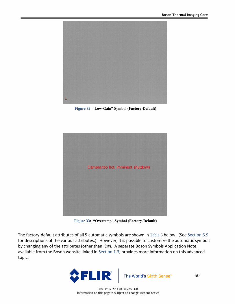
Boson Thermal Imaging Core
Doc. # 102-2013-40, Release 300
Information on this page is subject to change without notice
50
Figure 32: “Low-Gain” Symbol (Factory-Default)
Figure 33: “Overtemp” Symbol (Factory-Default)
The factory-default attributes of all 5 automatic symbols are shown in Table 5 below. (See Section 6.9 for descriptions of the various attributes.) However, it is possible to customize the automatic symbols by changing any of the attributes (other than ID#). A separate Boson Symbols Application Note, available from the Boson website linked in Section 1.3, provides more information on this advanced topic.

Boson Thermal Imaging Core
Doc. # 102-2013-40, Release 300
Information on this page is subject to change without notice
51
Table 5: Factory-default attributes of the automatic symbols
FFC Imminent
FFC Desired Table-Switch Desired
Low-gain Overtemp
ID# 10 11 12 13 14
Element Type Filled Rectangle
Outlined Rectangle
Arc Text Text
X Position 620 620 614 10 150
Y Position 50 50 45 470 200
Width 10 10 22 20 400
Height 10 10 22 20 25
Color 0000FF00 0000FF00 00FF0000 00762710 00FF0000
Z-position 0 0 0 0 0
Start Angle 0
End Angle 0
Font 1 1
Size 24 24
Alignment TOP LEFT TOP LEFT
ASCII Text L Camera too hot, imminent shutdown
6.9 Customized Symbols The Boson Release 2 configurations provide the option to specify custom symbol overlays. The camera supports several built-in symbol types, including rectangles, elliptical arcs, text, and lines, as exemplified in Figure 34. In addition to built-in symbols types, the camera also allows bitmaps to be uploaded to the camera for display. Width of the bitmap must be an integer multiple of 8.
NOTE: The Boson Graphical User Interface (GUI) is capable of opening PNG, BMP, and JPEG
files and converting them into the correct bitmap format.

Boson Thermal Imaging Core
Doc. # 102-2013-40, Release 300
Information on this page is subject to change without notice
52
Figure 34: Examples of Boson Symbol Types
Each symbol type has a variety of user-specified attributes, as listed below. Symbol attributes common to every symbol type:
• Symbol ID# (0 to 254): a handle for addressing the symbol when changing its attributes. Note that ID numbers 10 to 14 are pre-allocated for automatic symbols such as the FFC imminent icon. (See Section 6.8.) Changing the attributes of any of these symbol IDs will alter the appearance of the associated built-in symbol. See Table 5 for the ID# and other attributes of each automatic symbol.
• Symbol enable: 0 = not currently drawn, 1 = currently drawn • X and Y coordinates, where x=0, y=0 is the upper left of the image and x=639, y=511 is the
lower right. The upper-left corner of the symbol is placed at the specified coordinates. Note the symbol map/canvas is always 640x512 since symbol overlay occurs at the post-colorization tap in the pipeline, and that tap has 640x512 size regardless of sensor resolution. (See Section 7.9) It is not permissible to specify a location such that a portion of a symbol is outside the 640x512 canvas. (Attempting to do so will result in an error.)
• Transparency, where a value of 0 represents an opaque symbol and a value of 127 represents a completely transparent symbol. (Transparency values of 127-255 are invalid, and have undefined behavior.) Setting a transparency value greater than 0 allows a symbol to be shown without completing hiding the infrared imagery (or other symbols) behind it, as illustrated in Figure 35.
• Z-position, indicating a background (z=0) or foreground plane (z=1-255), used to determine precedence in the event of overlapping symbols. For example, a symbol with 0% transparency on the nth plane will completely hide a symbol located on the n-1 plane, as illustrated in Figure 35. (If two overlapping symbols both have the same z-position, the behavior is undefined.)

Boson Thermal Imaging Core
Doc. # 102-2013-40, Release 300
Information on this page is subject to change without notice
53
• Group number, from 1 to 19. It is possible to place multiple symbol ID#s into a common group. Doing so allows the entire group to be enabled/disabled and/or moved simultaneously. Moving a group causes the X/Y location of each symbol within the group to be updated automatically.
Other attributes for built-in symbol types • Color, specified as an RGBA index. This is a required attribute for all symbol types except
bitmaps. • Height / Width, specified in number of rows (1 to 512)_ / number of columns (1 to 640).
This is a required attribute for filled rectangles, outline rectangles, elliptical arc segments, filled ellipses, and text symbol types. For text symbols, the height and width refer to the bounding box for the text. If actual text width exceeds specified width, wrapping will be applied (potentially exceeding specified height).
• Start radius / end radius, from 0 to 360. This attribute applies to the arc segment symbol type only. It specifies the starting angle and ending angle, where angle = 0 is to the right and angle = 180 is to the left. The arc between the starting angle and ending angle is drawn clockwise. For example, the arc segment shown in Figure 34 has starting radius = 270 and ending radius = 180.
• Start point / end point, each specified as an x/y coordinate. This attribute applies to line segment symbol type only.
• Font type. 1 = built in font (Chrome Croscore Arimo font, used under authority of the Apache License, Version 2.0), 2 = user uploaded font file. This attribute applies to text symbol type only. All of the text shown in Figure 34 was generated with the built-in font.
• Font size. This attribute applies to text symbol type only and controls the nominal height of each character of text, in rows. For example, a font size of 32 results in a character height which consumes ~1/8th of the total image height.
• Justification. This attribute applies to text symbol type only, and the valid options are o LEFT_TOP o CENTER_TOP o RIGHT_TOP o LEFT_MIDDLE o CENTER_MIDDLE o RIGHT_MIDDLE o LEFT_BOTTOM o CENTER_BOTTOM o RIGHT_BOTTOM
• Text, in UTF-8 characters. The text string is a fixed-width, null-terminated buffer containing exactly 128 bytes. This attribute applies to text symbol type only.

Boson Thermal Imaging Core
Doc. # 102-2013-40, Release 300
Information on this page is subject to change without notice
54
Figure 35: Examples of Overlapping Symbols, Illustrating Transparency and Z-Location
A separate Boson Symbols Application Note, available from the Boson website linked in Section 1.3, provides many more examples and more detailed treatment of the custom-symbols feature.
6.10 Start-up Splash Screen Release 2 configurations of Boson provide the option of outputting one or two user-specified splash screens at start-up, such as a company logo and camera configuration data. The splash screens are displayed consecutively, Splash Screen 1 first, possibly followed by Splash Screen 2 if one has been uploaded to the camera. The lengths of time that each splash screen is displayed, Splash1 Duration and Splash2 Duration, are variable in millisecond increments from 0 to 120,000 msec. If the sum of Splash1 Duration and Splash2 Duration is less than the time required for the camera to transition out of “booting” state to a fully-operational state (see Section 7.1 for a description of start-up states), display of the final splash screen is automatically extended. By factory-default, a uniform black splash screen is displayed for the minimum booting time, and there is no second splash screen.
Splash screens can be uploaded to the camera in .PNG format in either 320x256 or 640x512 resolution. If a 320x256 splash screen is provided, it will be centered within a 640x512 color border, as exemplified in Figure 36. The border color, Splash1 Background Color and/or Splash2 Background Color, is user-selectable.

Boson Thermal Imaging Core
Doc. # 102-2013-40, Release 300
Information on this page is subject to change without notice
55
(a) Example 320x256 splash screen, centered within a color border
(b) Example 640x512 splash screen (output with no border)
Figure 36: Example splash-screens, 320x256 and 640x512 resolution
NOTE: Splash screens are only properly displayed on video channels configured for post-
colorization output. The post-colorization output tap has 640x512 size regardless of the sensor
resolution. (See Section 7.9.)

Boson Thermal Imaging Core
Doc. # 102-2013-40, Release 300
Information on this page is subject to change without notice
56
6.11 Field Calibration Most configurations of Boson include a set of factory-calibrated NUC terms which compensate for temperature effects, pixel response variations, lens-illumination roll-off, and out-of-field irradiance. For such configurations, the generation and application of NUC terms is transparent to the user and requires no external intervention or support. However, there are three notable exceptions to the above, each of which benefit from a one-time calibration process performed by the user:
a) The Boson lens-less configuration
b) A Boson installed behind a window or other optical assembly, resulting in a change to the illumination pattern onto the focal plane array.
c) A Boson installed in an environment which significantly affects self-heating, for example in an insulative enclosure or in a convective air flow. As a rule of thumb, re-calibration is recommended if the installation of the camera in the operating environment causes its steady state temperature to be more than one Celsius degree hotter or cooler than it would otherwise be when operated in the same ambient temperature in still-air with no enclosure.
NOTE: Exposing any thermal camera to rapid thermal transients will reduce the effectiveness
of the calibration and the quality of the image. For best results, the Boson camera should be
isolated from the thermal effects of window heaters, variable fans, power circuits, electric motors,
or similar intermittent thermal sources, as noted in Section 9.4.
The calibration process requires exposing the camera in its final installation condition (e.g., in enclosure behind a window if applicable) to two different blackbody temperatures (e.g., room temperature and 20C above room temperature). The Boson Graphical User Interface (GUI) sequences all the steps required to complete the calibration process. For a detailed tutorial on using the GUI, refer to FLIR’s Lens Calibration Application Note, available from the Boson website linked in Section 1.3.
6.12 Diagnostic Features Boson provides a number of diagnostic features, more completely defined in the sections that follow.
6.12.1 Test Patterns Boson provides capability to display a number of test patterns, two of which are illustrated in Figure 37. The test patterns are intended primarily to adjust display properties and/or for diagnostic purposes (for example, to verify the core is providing a valid output).

Boson Thermal Imaging Core
Doc. # 102-2013-40, Release 300
Information on this page is subject to change without notice
57
(a) Checkerboard test pattern
(b) Vertical-shade test pattern
Figure 37: Two of the Boson test patterns (shown in both White-Hot and Rainbow palettes)
6.12.2 Camera Temperature Boson provides capability to report its temperature via the Camera Temperature status variable. Accuracy of the measurement is +5Co. This temperature represents that of the sensor and is the value used to determine the proper NUC table (see Section 5.2) and to trigger FFC (see Section 6.3). Boson also provides capability to report the temperature of its internal signal-processing engine via the Core Temperature status variable. This temperature is the value used by the overtemp logic described in Section 7.2.

Boson Thermal Imaging Core
Doc. # 102-2013-40, Release 300
Information on this page is subject to change without notice
58
6.12.3 Status Indicators Boson provides a number of status indicators, reported via the telemetry line (see Section 6.4), via
the CCI, and in some cases as optional symbol overlays on the video signal. These indicators are listed
below. See the referenced sections for context and/or more detailed information.
NOTE: The text below describes the factory-default location and appearance of each symbol
overlay, but it is possible to change any attribute of these status-indicating symbols. For example,
rather than a solid green rectangle appearing in the upper right of the video signal during FFC, it
is possible to configure Boson to display text or any other symbol (including an uploaded bitmap
file) at any location. It is also possible to disable any or all of the status-indicating symbols such
that they do not appear.
■ FFC State: The FFC State variable provides information about the FFC event (i.e., has it been
initiated since start-up, is it imminent, is it in progress, is it complete). Section 7.6 defines
each of the FFC states. By factory default, a small solid green square will appear in the
upper right of the post-colorization video signal when FFC state = “FFC imminent” or “FFC
In Progress”. (See Figure 29 in Section 6.8.)
■ FFC Desired: When operating in manual or external FFC mode, the FFC Desired flag is
used to signal the user to command FFC at the next possible opportunity. In automatic
FFC mode, the flag is never set because an automatic FFC takes place instead. See
Section 7.6 for detailed description of the conditions which cause the flag to be set. By
factory default, a small unfilled square (green border) will appear in the upper right of the
post-colorization video signal whenever the FFC Desired flag is set. (See Figure 30 in
Section 6.8.)
■ Table Switch Desired: When operating in manual or external FFC mode, the Table Switch
Desired flag is set when the camera is operating outside the range of the current NUC
table. (See Section 5.2 for more details.) When in automatic FFC mode, this flag is never
set because instead an automatic table switch takes place. By factory default, a red circle
will appear in a location which circumscribes the FFC Desired symbol whenever the Table
Switch Desired flag is set. (See Figure 31 in Section 6.8.)
■ Current NUC Table: The Current NUC Table variable indicates the current NUC table in which
the camera is operating. As described in Section 5.2, a value of 0 indicates Boson is in low-
gain state while a value of 1, 2, or 3 indicates Boson is in high-gain state. There is no symbol
overlay symbol to indicate this status directly. However, when Boson is operating in low-gain
state, a purple “L” will appear by factory-default in the lower-left of the post-colorization
video signal. (See Figure 32 in Section 6.8.)

Boson Thermal Imaging Core
Doc. # 102-2013-40, Release 300
Information on this page is subject to change without notice
59
■ Desired NUC Table: The Desired NUC Table variable indicates the NUC table the camera will
switch to upon receipt of the Table Switch command. See Section 6.2 and Section 7.6 for
more information regarding the Table Switch command. There is no symbol overlay symbol
to indicate this status. However, when Desired NUC Table differs from Current NUC Table,
the Table Switch Desired flag described above is set.
■ Overtemp: The Overtemp flag indicates the camera has exceeded its maximum operating
temperature and will automatically enter Low-Power state. See Section 7.2 for more
information regarding the Overtemp feature and Low-Power state. By factory default, a text
warning will appear in the center of the display whenever the Overtemp flag is set. (See
Figure 33 in Section 6.8.)
■ Low-Power State: The Low-Power flag indicates the camera is in Low-Power state, typically
the result of an overtemp event. See Section 7.2 for more information regarding the
Overtemp feature and Low-Power state. There is no symbol overlay associated with Low-
Power State because the video signal is disabled when in this state. The telemetry line
will enable the Low-Power flag one frame before Boson enters the Low-Power state.
6.13 Upgradeability / Backward Compatibility Boson can be updated with new software releases via the CCI. The upgrade is easily accomplished using the Boson Graphical User Interface (GUI). A more detailed Boson Software Upgrade Application Note provides step-by-step directions for those users who wish to update Boson’s software from their own host platform rather than via the Boson GUI. This App Note is available from the Boson website linked in Section 1.3. Boson provides fault-tolerant software upgradeability, meaning that if power to the camera is disrupted during an upgrade event, the core is capable of rebooting with the functionality required to repeat the upgrade process. All future releases of Boson software will be backwards compatible with all production versions of Boson. In other words, upgrading a production core with an authorized software release will not result in a loss of function or performance.
NOTE: Not all feature improvements planned for later releases will necessarily work when a
fielded camera is upgraded because some may require factory calibration to function properly.
However, in all cases, a new feature will at worst simply not function rather than causing an
upgraded core to behave erroneously.

Boson Thermal Imaging Core
Doc. # 102-2013-40, Release 300
Information on this page is subject to change without notice
60
6.13.1 Configuring a Release 2 Camera to Behave Identically to a Release 1 Camera The key differences of Boson Release 2 relative to Release 1 are listed below. Note that all changes are additional capabilities. For each difference, the steps required to configure a Release 2 camera to behave exactly like a Release 1 camera are described.
• Symbol overlay. (See Sections 6.8 and 6.9 for a detailed description.) Each of the system symbols such as the FFC imminent icon and overtemp icon can be enabled/disabled individually. To configure a Release 2 camera such that it displays no symbols whatsoever (like Release 1), there is also a global symbol enable/disable.
• Splash screen. (See Section 6.10 for a detailed description.) By factory default, a flat black splash screen is enabled on a Release 2 Boson camera at start-up for the minimum time required for the camera to boot up and enable IR video. In the Release 1 configuration, there is no splash screen as the function did not exist; instead random imagery appeared on the display signal until IR video was enabled. To configure a Release 2 camera such that it has no splash screen at start-up and instead displays random imagery like a Release 1 camera, the default splash screen can be erased via command.
• Overtemp protection. (See Section 7.2 for a detailed description.) By factory default, a Release 2 Boson camera will automatically enter a non-imaging low-state mode when its internal temperature exceeds its maximum safe value for more than 10 seconds. It is not recommended to override this safety feature since extended operation in an overtemp state is likely to result in permanent damage and will void the warranty. However, in certain critical scenarios (for example, a firefighting application), it may be preferred to risk permanent damage rather than have the camera automatically enter the lower-power state. In such applications, it is possible to disable automatic entry into the low-power state. The overtemp warning will be generated even if the automatic low-power state is overridden, but it is possible to disable the on-screen symbol which provides the warning via command. (The status bit and overtemp counter in the telemetry line cannot be disabled.)
• Non-volatile FFC. (See Section 7.6.1 for a detailed description) Release 2 Boson cameras are delivered without a stored non-volatile FFC (NVFFC) map and will therefore behave identical to a Release 1 Boson regarding start-up behavior. If a NVFFC map is stored after delivery, start-up behavior may differ from a Release 1 configuration (as described in Section 7.6), but simply erasing the map via command will result in start-up behavior identical to Release 1.
• Supplemental FFC. (See Section 5.2 for a more-detailed description of SFFC.) Release 2 Boson cameras which are shipped with a factory-installed lens will include a factory-calibrated Supplemental FFC (SFFC) map. SFFC is intended to improve non-uniformity compared to a Release 1 camera, and it is not recommended to deliberately disable it unless operating in external FFC state. However, the option to do so is provided.

Boson Thermal Imaging Core
Doc. # 102-2013-40, Release 300
Information on this page is subject to change without notice
61
• More frequent FFC at start-up. As described in Section 6.3, Release 2 configurations of Boson will perform more frequent FFC at start-up by factory-default. It is not recommended to change the FFC Start-up Period variable, but setting it to 0 will disable the more frequent FFC at start-up, resulting in behavior identical to Release 1.
• Lower power. As described in Section 12.2, Release 2 Boson configurations consume less power than Release 1 configurations. This is primarily the result of more efficient signal processing and clock management. There is no direct way to intentionally increase the power consumption of a Release 2 Boson to the same level as a Release 1 Boson, but it is assumed no user would want to do so.

Boson Thermal Imaging Core
Doc. # 102-2013-40, Release 300
Information on this page is subject to change without notice
62
7 Operating States and Modes Boson provides a number of operating states and modes, more completely defined in the sections which follow. Generally speaking, modes of operation are user-selectable (i.e., the camera operates this way or that way depending upon user selections) whereas states are camera behaviors or operating conditions which take place automatically.
■ Start-Up States, page 62 ■ Overtemp and Low-Power States, page 63 ■ Averager Modes, page 66 ■ Telemetry Modes, page 66 ■ Gain Modes and States, page 67 ■ FFC Modes and States, page 68 ■ Lens Modes, page 72 ■ AGC Modes, page 73 ■ CMOS Video-Tap Modes, page 73 ■ CMOS Color-Encoding Modes, page 74 ■ CMOS Output Modes, page 77
7.1 Start-Up States Boson provides four start-up states. In most cases, the transitions between states are the result of
explicit action from the user, indicated by bold text in Figure 38. The transition from “booting” to
“fully booted” is automatic, requiring no user intervention. The four states and the transitions
between them are described in more detail below.
Figure 38: Boson Start-Up States

Boson Thermal Imaging Core
Doc. # 102-2013-40, Release 300
Information on this page is subject to change without notice
63
■ Off: When no voltage is applied, Boson is in the Off state. In the off state, no camera
functions are available, and the camera consumes no power.
■ In Reset: When voltage is applied but the reset pin asserted, Boson is in the “In Reset”
state. In the “In Reset” state, no camera functions are available, and the camera consumes
minimal power (~65mW). Note that the Reset pin is asserted low.
■ Booting: In the “Booting” state, Boson is loading its program and initializing itself for full
operation. Note that the reset pin must be floating for Boson to exit from the “Booting”
state to the “Fully-booted” state.
■ Fully Booted: In the “Fully-booted” state, Boson is fully functional, producing imagery, and
capable of responding to commands via the CCI. Typical start-up time to the fully booted
state is 3.0 seconds for the 320 configuration and 4.4 seconds for the 640 configuration.
NOTE: It is not strictly necessary to connect the reset pin to power on the Boson camera, but it
must be floating when the camera is in the “Booting” state, not tied to 3.3V or ground.
NOTE: It is recommended to avoid sending commands via the CCI while the camera is in any
state other than ‘fully booted’. This is indicated by output of imagery on the CMOS and/or USB
channels.
7.2 Overtemp Modes and States
The Release 2 configuration of Boson provides two overtemp shutdown modes:
■ Enabled (factory default): The camera automatically transitions to a low-power state when internal core temperature exceeds the maximum safe value. The camera is capable of responding to commands in the low-power state, but the image pipeline is deliberately disabled to reduce power dissipation and thereby reduce core temperature. As illustrated in Figure 39, the transition between the normal imaging state and the low-power state is via a temporary “overtemp” state, as described below.
■ Disabled: The camera transitions to the overtemp state but not to the low-power state in response to core temperature exceeding the maximum safe value. This mode is provided strictly for mission-critical applications (such as firefighting) in which it is essential to extend mission life as much as possible, even at risk of permanent damage. Because of the high risk of damage resulting from extended operation in the overtemp state, operation in the “Overtemp Shutdown Disabled” mode voids the camera warranty.

Boson Thermal Imaging Core
Doc. # 102-2013-40, Release 300
Information on this page is subject to change without notice
64
Figure 39: Boson Overtemp and Low-power States
■ Normal Imaging State to Overtemp State: When the camera’s internal core temperature
exceeds its maximum safe value, 105C, the camera automatically transitions to the overtemp
state. In this state, an overtemp status flag is set (Bit 8 of the status bits provided in columns 38 –
41 of the telemetry line, see Section 6.4), an overtemp event counter is incremented (columns 83
and 84 of the telemetry line), and the on-screen warning shown in Figure 33 is provided on the
post-colorize / symbol overlay video tap. (It is possible to disable the display of the on-screen
warning. See Section 6.8.) A countdown timer starts when the camera first enters the overtemp
state. The factory-default timeout period of the countdown timer is 10 seconds. ■ Overtemp State to Normal-Imaging State: If core temperature falls into a safe operating
range (< 100C) while the camera is still in overtemp state, a transition back to normal-imaging
state takes place. The overtemp status flag is cleared, the on-screen warning is removed, and the
countdown timer is stopped and restored to its starting value. ■ Ovetemp State to Low-Power State: Unless overtemp shutdown mode has been set to
“disabled” (as described above), the camera automatically transitions from overtemp to
the low-power state when the overtemp countdown timer times out. In low-power state,
the camera continues to respond to commands sent over the CCI, but the image-
processing pipeline is disabled, causing no further output frames to be provided at the
video channels. The fact that the camera is in the low-power state can be ascertained via

Boson Thermal Imaging Core
Doc. # 102-2013-40, Release 300
Information on this page is subject to change without notice
65
a low-power status flag readable via the CCI. The same status is also provided in the
telemetry line (Bit 7 of the status bits provided in columns 38 – 41 of the telemetry line) on the
very last frame before the camera transitions from overtemp state to low-power state. It
is also worth noting that the camera’s core temperature value can be read via the CCI
while in the low-power state.
■ Low-Power State to Normal Imaging State. The only exit from the low-power state is by
toggling camera power or by reset (by asserting the reset signal or via a reset command).
Note that if the camera’s core temperature is still above maximum safe value after reset,
the entire process will start over again. That is, the camera will immediately transition
back into the overtemp state.
The factory default value of the timeout period of the overtemp countdown timer is 10 sec, but it can be varied between 0 and 20 seconds. A value of 0 is treated as an exception. Instead of causing the camera to immediately transition from overtemp to non-imaging state (i.e., a zero-second stay in the overtemp state), a value of 0 causes the camera to never transition to the low-power state. That is, a value of 0 is effectively treated like infinity and is therefore an alternative means of preventing the automatic transition to low-power state.
NOTE: It is highly recommended to leave the overtemp shutdown mode at “enabled” and the
timeout period of the overtemp countdown timer to a value between 1 and 20 seconds. Setting
overtemp shutdown mode to “disabled” and/or setting the timeout period to 0 seconds (which
is treated as an exception, as described above) voids the camera warranty.
NOTE: See Section 6.12.2 for the distinction between Camera Temperature and Core
Temperature. The latter is the relevant variable for triggering the overtemp and low-power states.
NOTE: See Section 9.1 for recommended heatsinking practices to avoid an overtemp condition.

Boson Thermal Imaging Core
Doc. # 102-2013-40, Release 300
Information on this page is subject to change without notice
66
7.3 Averager Modes
Boson provides two averager modes affecting the video output signal:
■ Averager disabled (factory default) ■ Averager enabled
The mode is selected using the Averager Enable command. As described in Section 5.1, the primary
benefit of enabling the averager is power reduction for those applications which do not require a high
frame rate.
NOTE: By factory-default, the frame averager is disabled. Intended use case is that the averager
is enabled once at start-up and optionally saved as a power-on default. Toggling the averager off
and on more than once per power cycle is not recommended and may result in video instability.
7.4 Telemetry Modes Boson provides three telemetry modes affecting the CMOS output signal:
■ Telemetry enable is either true or false. Factory-default value is true.
■ Telemetry location determines whether the telemetry line is provided on the first row (as
a header) or on the last row (as a footer) of each video frame. Factory-default value is
header.
■ Telemetry encoding determines how the telemetry line is provided on the CMOS pins:
• 16b mode: In this mode, the factory-default, each telemetry datum is provided as a 16b
word on cmos_data[0-15].
• 8b mode: In this mode, each telemetry datum is provided as two consecutive bytes
(big-endian order) on cmos_data[0-7]. Consequently, twice as many clock periods are
required to transmit the data, so each datum takes up twice as many “pixels” compared
to 16m mode.
• 8b-swapped mode (“Y”mode): This mode is identical to 8b mode except bytes are
provided in little-endian order (least-significant byte provided first).
See Section 6.4 for a complete description of the telemetry line.
NOTE: In the current product release, telemetry mode only affects the CMOS output as
telemetry is not an option for the USB video channel. It is anticipated that telemetry will be
optional on the USB channel in a later field-upgradeable software release.

Boson Thermal Imaging Core
Doc. # 102-2013-40, Release 300
Information on this page is subject to change without notice
67
7.5 Gain Modes and States As described in Section 6.2, Boson provides two gain states: high and low. However, there are 3 gain
modes which determine in which gain state it operates:
■ High-gain mode (factory default): Boson operates in high-gain state only and does not signal Table Switch Desired in response to scene conditions.
■ Low-gain mode: Boson operates in low-gain state only and does not signal Table Switch Desired in response to scene conditions.
■ Automatic gain mode: In automatic FFC mode (see Section 7.6), Boson automatically transitions between high-gain state and low-gain state based on scene conditions and user-specified parameters. In manual and external FFC mode, Table Switch Desired is set based on scene conditions and user-specified parameters. See Section 6.2 for a detailed description of the parameters.
NOTE: With Release 1 software, automatic gain mode and AGC Information-Equalization
mode are mutually exclusive, and an error results from trying to enable one while the other is
already enabled. With Release 2 software, the two features are not mutually exclusive.

Boson Thermal Imaging Core
Doc. # 102-2013-40, Release 300
Information on this page is subject to change without notice
68
7.6 FFC Modes and States
Boson provides three different FFC modes:
■ Automatic (factory default): The camera periodically performs automatic FFC in response to a number of conditions, as described in more detail in Table 6. (See Section 6.3 for a more general description of the FFC feature.)
■ Manual: The camera may perform automatic FFC at start-up, depending upon whether or not a valid non-volatile FFC map is stored (as described in Section 7.6.1). Thereafter, it only performs FFC upon command. The camera sets an FFC Desired flag under a number of conditions described in Table 6.
■ External: The camera never performs FFC except upon receipt of the “Do FFC” command. Moreover, it does not utilize the internal shutter for FFC but instead must be imaging a uniform external source before FFC is commanded. (The uniform source must be held in place until the FFC State changes from FFC In Progress to FFC Complete, as described below.) The camera sets an FFC Desired flag under a number of conditions described in Table 6.
NOTE: When operating in external FFC mode, the SFFC correction should be disabled since
the SFFC correction is invalid when an external source is used for FFC. See Section 5.2 for a
description of SFFC.
Table 6: Camera behavior in each FFC Mode in response to various operating conditions
Condition Behavior in Auto FFC mode
Behavior in Manual
FFC mode
Behavior in External FFC mode
Start-up Automatic FFC take place
If a valid NVFFC map is stored (see Section 7.6.1), it is loaded. Otherwise, automatic FFC takes place.
If a valid NVFFC map is stored (see Section 7.6.1), it is loaded. Otherwise FFC Desired flag is set.
Commanded FFC (Do FFC) FFC takes place FFC takes place; FFC Desired is cleared
Frame Counter – Frame Counter at Last FFC > FFC Period (see note 1)
Automatic FFC takes place
FFC Desired is set
|Camera Temp – Camera Temp at Last FFC| > FFC Delta Temp (see note 1 and note 2)
Automatic FFC take place
FFC Desired is set

Boson Thermal Imaging Core
Doc. # 102-2013-40, Release 300
Information on this page is subject to change without notice
69
Condition Behavior in Auto FFC mode
Behavior in Manual
FFC mode
Behavior in External FFC mode
Camera is outside the temp span of the current high-gain NUC Table while in high-gain state (see Section 5.2)
Automatic NUC Table switch takes place, followed by automatic FFC
Table Switch Desired is set. Desired NUC Table is set to the optimal NUC-table value (which will differ from Current NUC Table).
While in automatic gain mode, scene conditions are sufficient to trigger a gain-state change (i.e., from high to low or vice versa). See Section 6.2.
Automatic gain switch takes place, possibly followed by automatic FFC as described in note 3.
Table Switch Desired is set. Desired NUC Table set to the optimal NUC-table value (which will differ from Current NUC Table).
Table Switch Commanded while Table Switch Desired is set.
n/a (Table Switch Desired is never set.)
NUC table switch takes place and Table Switch Desired is cleared, possibly followed by automatic FFC as described in note 3.
NUC table switch takes place and Table Switch Desired is cleared, possibly followed by FFC Desired being set as described in note 3.
Commanded switch to low-gain mode while in high-gain state or commanded switch to high-gain mode while in low-gain state.
Gain switch takes place, possibly followed by automatic FFC as described in note 3.
Gain switch takes place, possibly followed by FFC Desired flag being set as described in note 3.
• Note 1: Frame Counter, Frame Counter at Last FFC, Camera Temp, Camera Temp at Last FFC are all status variables which are provided via the telemetry line (see Section 6.4) or via command on the CCI. FFC Period and FFC Delta Temp are both user-selectable parameters which can be specified via the CCI, as further described in Section 6.3.
• Note 2: From start-up until a time specified by FFC Start-up Period, the condition is instead |Camera Temp – Camera Temp at Last FFC| > FFC Delta Temp / 3, as described in Section 6.3.
• Note 3: Boson is capable of transitioning between high-gain and low-gain state without an intervening FFC operation. Separate FFC maps are maintained for high-gain and low-gain states, as well as separate values of Frame Counter at Last FFC and Camera Temp at Last FFC. When transitioning between gain states, whether the result of an automatic switch or commanded switch, automatic FFC or a set of the FFC Desired flag only occurs if elapsed time since FFC in that state and/or temperature change since the last FFC in that state dictate that an FFC take place. See the example below.
Examples of FFC behavior when transitioning between gain states:
• With the camera in automatic FFC mode and high-gain mode, FFC is commanded while Camera Temperature has a value of 3000 (300.0K). Following FFC, Camera Temperature at Last FFC = 3000 (300.0K). FFC Temp Delta is at its factory-default value, 30 (3.0C).
• When Camera Temperature = 301.0K, the camera is commanded into low-gain mode for the first time. Gain switch takes place, and now Camera Temperature at Last FFC = 0 since FFC has never been

Boson Thermal Imaging Core
Doc. # 102-2013-40, Release 300
Information on this page is subject to change without notice
70
performed in low-gain state. Consequently, automatic FFC takes place, and now Camera Temperature at Last FFC = 3010 (301.0K).
• When the camera is at 302.0K, the camera is commanded into high-gain mode. Camera Temperature at Last FFC = 3000 again. No FFC takes place and FFC Desired is not set since |Camera Temperature - Camera Temperature at Last FFC| < FFC Temp Delta.
• When the camera is at 303.0K, it is commanded back to low-gain state. Gain switch takes place, and Camera Temperature at Last FFC = 3010 again. No FFC takes place and FFC Desired is not set since |Camera Temperature - Camera Temperature at Last FFC| < FFC Temp Delta.
• The camera continues to heat while in low-gain state until it reaches 304.0K. Now an automatic FFC takes place because |Camera Temperature - Camera Temperature at Last FFC| > FFC Temp Delta. Following FFC, Camera Temperature at Last FFC = 3040 (304.0K) and FFC Desired is cleared.
• With temperature still at 304.0K, the camera is commanded to high-gain mode. Now Camera Temperature at Last FFC = 3000, and another automatic FFC takes place because |Camera Temperature - Camera Temperature at Last FFC| > FFC Temp Delta.
While the FFC mode defines when and how Boson performs FFC, the FFC state pertains to the FFC event itself. There are four FFC states, as illustrated in Figure 40.
1. FFC not initiated (power-on default): In this state, Boson applies no FFC terms. In automatic FFC
mode, this state is never seen because Boson always performs automatic FFC at start-up.
2. FFC imminent: The camera only enters this state when it is operating in automatic FFC mode. The
camera enters “FFC imminent” state at a user-specified period prior to initiating an automatic FFC
(factory default = 2 sec). The intent of this status is to warn the user that an FFC is about to occur.
3. FFC in progress: Boson enters this state when FFC is commanded from the CCI or when an
automatic FFC event is initiated. During each FFC event, the shutter is closed (if in automatic or
manual FFC mode), frames of sensor data are collected to generate the correction map, the
shutter is opened, and the new FFC map is applied.
Boson’s video output is “frozen” throughout the “FFC in progress” state. That is, the last valid
frame prior to entering “FFC in progress” is repeated throughout the event. (The telemetry
line is not frozen, only the thermal image.)
4. FFC complete: Boson automatically enters this state whenever a commanded or automatic FFC is
completed.

Boson Thermal Imaging Core
Doc. # 102-2013-40, Release 300
Information on this page is subject to change without notice
71
Figure 40: Boson FFC States
7.6.1 Non-volatile FFC The Boson Release 2 configuration provides the option to store the current FFC map to non-volatile memory. The intent of the feature is to support a faster transition from start-up to useable imagery, particularly in those cases where the camera has only been powered down briefly since the last FFC. When the camera receives the command to store the current FFC map, it also stores the value of “Camera temperature at last FFC” (the same value reported in the telemetry line, as shown in Table 4 of Section 6.4) as well as the current NUC table. (See note 2 of Table 6 for a description of NUC tables.) The next time the camera powers up, the decision to utilize the stored NVFFC map depends upon FFC mode, as described below.
• Automatic FFC: The camera does not load the stored NVFFC map but always performs automatic FFC instead. If the option of a faster start-up is desired, the power-on default FFC mode should be set to manual mode instead.

Boson Thermal Imaging Core
Doc. # 102-2013-40, Release 300
Information on this page is subject to change without notice
72
• Manual FFC: If the stored NVFFC map was generated in the same NUC table as the start-up NUC table, then it is loaded and applied. Otherwise, an automatic FFC takes place under the assumption that the stored map is invalid for the current conditions (i.e., will result in sub-optimal image quality). If the map is loaded, the value of “Camera temperature at last FFC” will be set to the value stored with the NVFFC map, and the value of “Frame counter at last FFC” will be set to 0. Note that the FFC Desired flag may be set immediately after the NVFFC map is loaded, assuming the difference between current camera temperature and “Camera temperature at last FFC” exceeds the value of FFC Delta Temp, as depicted in Table 6.
• External FFC: If the stored NVFFC map was generated in the same gain state as the start-up gain state (see Sections 6.2 and 7.5), then it is loaded and applied. Otherwise, no FFC offset is applied (and the FFC Desired flag will be set) under the assumption that the stored map is invalid for the current conditions. If the map is loaded, the value of “Camera temperature at last FFC” will be set to the value stored with the NVFFC map, and the value of “Frame counter at last FFC” will be set to 0. Note that the FFC Desired flag may be set immediately after the NVFFC map is loaded, assuming the difference between current camera temperature and “Camera temperature at last FFC” exceeds the value of FFC Delta Temp, as depicted in Table 6.
NOTE: Generally speaking, it is always preferred to generate a fresh FFC map at start-up rather
than relying on a stored, potentially stale NVFFC map. The NVFFC feature is intended primarily
for the case in which a camera has only been powered down briefly since the previous FFC. The
NVFFC feature does not preclude the need for shutterless configurations to perform FFC at start-
up.
7.7 Lens Mode Boson provides two lens modes:
■ Lens 0 (factory default)
■ Lens 1 The primary intent of multiple lens modes is to support a dual-FOV lens assembly. For such a lens, the illumination pattern and the out-of-field irradiance may differ between the two FOVs, in which case better image quality can be obtained by switching the applied correction terms when switching the FOV. This can be accomplished by toggling the lens mode, which causes the following terms to be swapped:
• Lens-gain map. (See Section 5.2)
• SFFC map. (See Section 5.2)

Boson Thermal Imaging Core
Doc. # 102-2013-40, Release 300
Information on this page is subject to change without notice
73
• NVFFC map. (See Section 7.6.1) The NVFFC map is only loaded at start-up, and the power-on default selection of lens mode determines which of the two will be loaded. Switching lens mode after start-up will not cause the other NVFFC map to load. Instead, the current FFC map will continue to be applied.
NOTE: For any Boson configuration which includes a factory-installed lens, Lens 0 is factory-
calibrated and Lens 1 is empty. For lensless configurations, both Lens 0 and Lens 1 are empty,
as it is intended that a lens-calibration procedure will be performed by the user after installing a
lens assembly.
7.8 AGC Modes As described in Section 6.5, Boson provides two AGC modes:
■ Information-Based Equalization Mode Enabled (factory default): AGC transfer function is based on the amount of information in the scene. That is, portions of the scene which contain variations (e.g., foliage) are weighted more heavily than portions which only vary gradually (e.g., sky).
■ Information-Based Equalization Mode Disabled: AGC transfer function weights all pixels equally.
NOTE: Unlike Release 1, automatic gain mode and AGC Information-Based Equalization are
not mutually exclusive in a Release 2 Boson. That is, it is possible to enable automatic gain mode
and Information-Based Equalization mode simultaneously.
7.9 CMOS Video-Tap Modes As described in Section 5 and shown again in Figure 41, there are multiple locations in the signal pipeline where video can be tapped for output on the CMOS channel. Boson provides the following CMOS video-tap modes:
■ Pre-AGC (16-bit) (factory default): The output is linearly proportional to incident irradiance; output resolution is the same as FPA resolution (e.g., 320x256 or 640x512). Data is provided on CMOS_Data[0:15]. Note that AGC settings, zoom settings, and color-encoding settings have no effect on the output signal at this tap point.
■ Post-AGC / Pre-Zoom (8-bit): The output is contrast enhanced via the AGC algorithm; output resolution is the same as FPA resolution. Data is provided on CMOS_Data[0:7]. Note that zoom settings and color-encoding settings have no effect on the output signal at this tap point.

Boson Thermal Imaging Core
Doc. # 102-2013-40, Release 300
Information on this page is subject to change without notice
74
■ Post-Zoom, Post-Colorize (various bit-width options depending upon color-encoding mode, see Section 7.10): The output is stretched to 640x512 resolution regardless of array format, and the displayed field of view is a function of the user-specified zoom parameters. The output is transformed to color space using the specified color palette (see Section 6.7) and specified color encoding mode (see Section 7.10).
Figure 41: Boson Signal Pipeline
7.10 CMOS Color-Encoding Modes Boson provides the following color-encoding modes which affect formatting of the output video signal when the post-colorize tap is selected:
■ YCbCr 4:2:2 (16-bit per pixel) (factory-default): The signal consists of a luminance channel (8 bits per clock on CMOS_Data[0:7]), a blue chrominance channel (8 bits on each even clock cycle on CMOS_Data[8-15]), and a red chrominance channel (8 bits on each odd clock cycle on CMOS_Data[8-15]).
■ YCrCb 4:2:2 (16-bit per pixel): The signal is identical to YCbCr except the red and blue chrominance channels are swapped. That is, the red chrominance channel is provided on the even clock cycle and the blue chrominance channel on the odd clock cycle.
NOTE: Only YCbCr 4:2:2 and YCrCb 4:2:2 are validated in the current software release. All
remaining options shown below are capable of being selected but are not currently validated.
FLIR does not recommend relying on any of these without thoroughly testing in the end
application.
■ RGB 8:8:8 (24-bit per pixel): The signal consists of a red channel (8 bits per clock on CMOS_Data[0:7]), a green
channel (8 bits per clock on CMOS_Data[8-15]), and a blue channel (8 bits per clock on CMOS_Data[16-23]). ■ BGR 8:8:8 (24-bit per pixel): The signal is identical to RGB 8:8:8 except the blue and red channels are swapped.
That is, the blue channel is provided on CMOS_Data[0:7] and the red channel on CMOS_Data[16:23]. ■ YCbCr 4:2:2 muxed (16-bit per pixel, 2 clocks per pixel): The luminance and chrominance channels are time-
multiplexed on CMOS_Data[0:7]. Specifically, the luminance is provided on clock cycles n and n+2, the blue chrominance channel on clock cycle n+1, and the red chrominance channel on clock cycle n+3, for n = 0, 4, 8…. The CMOS pixel clock rate is doubled when in this mode.

Boson Thermal Imaging Core
Doc. # 102-2013-40, Release 300
Information on this page is subject to change without notice
75
■ YCrCb 4:2:2 muxed (16-bit per pixel, 2 clocks per pixel): The signal is identical to YCbCr 4:2:2 muxed except the order of the red and blue chrominance channels are swapped. That is, the red chrominance channel is provided on clock cycles n+1 and the blue chrominance channel on cycles n+3. The CMOS pixel clock rate is doubled when in this mode.
■ RGB 8:8:8 muxed (24-bit per pixel, 2 clocks per pixel): The red, green, and blue color channels are time-multiplexed on CMOS_Data[0:11]. Specifically, on even clocks cycles the red channel is provided on CMOS_Data[0:7] and the 4 LSBs of the green channel are provided on CMOS_Data[8:11]. On odd cycles, the MSBs of the green channel are provided on CMOS_Data[0:3] and the blue channel is provided on CMOS_Data[4:11]. The CMOS pixel clock rate is doubled when in this mode.
■ BGR 8:8:8 muxed (24-bit per pixel, 2 clocks per pixel): The signal is identical to RGB 8:8: muxed except the blue and red channels are swapped. That is, the blue channel is provided on CMOS_Data[0:7] on even cycles and the red channel on CMOS_Data[4:11] on odd cycles. The green channel encoding is unchanged. The CMOS pixel clock rate is doubled when in this mode.
For reference, the color encoding of each mode is depicted graphically in Figure 42. Note the CMOS color-encoding mode has no effect on the video signal unless CMOS video-tap mode is “post colorize”.

Boson Thermal Imaging Core
Doc. # 102-2013-40, Release 300
Information on this page is subject to change without notice
76
Color Mode
Clk CMOS_Data
23 22 21 20 19 18 17 16 15 14 13 12 11 10 9 8 7 6 5 4 3 2 1 0
YCbCr 4:2:2
0 Unused Cb[7:0] Y0[7:0]
1 Unused Cr[7:0] Y1[7:0]
YCrCb 4:2:2
0 Unused Cr[7:0] Y0[7:0]
1 Unused Cb[7:0] Y1[7:0]
RGB 8:8:8
B[7:0] G[7:0] R[7:0]
BGR 8:8:8
R[7:0] G[7:0] B[7:0]
YCbCr 4:2:2 muxed
0 unused Y0[7:0]
1 unused Cb[7:0]
2 unused Y1[7:0]
3 unused Cr[7:0]
YCrCb 4:2:2 muxed
0 unused Y0[7:0]
1 unused Cb[7:0]
2 unused Y1[7:0]
3 unused Cr[7:0]
RGB 8:8:8
muxed
0 unused G[3:0] R[7:0]
1 unused B[7:0] G[7:4]
BGR 8:8:8
muxed
0 unused G[3:0] B[7:0]
1 unused R[7:0] G[7:4]
Figure 42: Boson’s Various Color-Encoding Modes
Modes which are highlighted in gray have not yet been validated in the current product release.

Boson Thermal Imaging Core
Doc. # 102-2013-40, Release 300
Information on this page is subject to change without notice
77
7.11 CMOS Output Modes The final stage in the Boson signal pipeline is a multi-frame buffer. The CMOS output channel reads the front buffer while the signal pipeline writes a background buffer. Boson provides two CMOS output modes which affect the behavior of the CMOS channel in relation to the multi-frame buffer:
■ Continuous (factory-default): In this mode, the CMOS channel provides data at a regular cadence
(i.e., exact same clocks per frame period without exception). If the background buffer is still
being written when the front buffer has been fully read out, the front buffer is read out again,
resulting in a duplicated frame. This mode of operation is preferred for interfacing to a display
system which requires data at a regular interval.
NOTE: Since the frame rate of the sensor and frame rate of the output channel are nominally
identical, it is very uncommon for duplicated frames in continuous mode. The presence of a
duplicated frame can be detected via the frame counter in the telemetry line since the frame
counter does not increment for a duplicated frame.
■ One-shot: In this mode, the CMOS channel inserts idle time between successive frames in those
instances where there is not a back buffer ready for readout when the front buffer has been
completely read. Consequently, the number of clocks per frame period is not a constant but
can instead vary slightly. In this mode of operation, every frame is unique. This mode of
operation is preferred for interfacing to a frame grabber which can tolerate slight frame-rate
jitter.
NOTE: The CMOS Output mode has no effect on the USB video channel. The USB video
channel always operates in one-shot mode.
7.12 Analog Modes Boson provides the option of outputting a BT.656 signal using the pins normally used to provide the CMOS video channel. This capability is utilized by the the FLIR USB / Analog VPC Accessory (see Section 16.2) to obtain analog video output. There are three “analog modes”:
■ Analog Disabled (factory default): The CMOS channel is configured to output video according to the timing and logic described in Section 8.2.1.
■ NTSC: The CMOS channel is configured for BT.656 output at 60Hz frame rate, outputting 525 lines per frame (525/60).
■ PAL: The CMOS channel is configured for BT.656 output at 50Hz frame rate, outputting 625 lines per frame (626/50).

Boson Thermal Imaging Core
Doc. # 102-2013-40, Release 300
Information on this page is subject to change without notice
78
When the CMOS channel is configured for BT.656 output, cmos_vsync, cmos_hsync, and cmos_data_valid are unused, as are cmos_data[8-23]. That is, only cmos_pclk and cmos_data[0-7] are utilized, with the most-significant bit provided on cmos_data7, and the least significant bit provided on cmos_data0. Clock rate remains 27 MHz when the channel is configured for BT.656 output. There are several noteworthy caveats regarding Boson’s BT.656 output signal:
• The output is single-ended, not differential.
• Digital line alignment does not follow the BT.656 standard exactly. Specifically, in a strictly-compliant implementation, each video line begins with an EAV code, then blanking, then SAV code, then Video Data. In Boson, digital alignment is achieved by observing EAV/SAV pairs only when only the “H’ bit is changing, making it a non-standard implementation. FLIR has not seen any resulting problems from this.
• No scaling of BT.656 output (vertical or horizontal) is supported in Boson Release 1 and 2.
• FLIR has observed some image pulsing on older CRT monitors. LCD monitors are recommended for optimal analog display.
• BT.656 limits output to values within the range 16 to 235. Because the BT.656 channel and the USB channel both receive data from a common output buffer, the USB video signal will also be limited to values within the range 16 to 235 when Analog mode is set to NTSC or PAL.
When Boson is mated with the FLIR USB / Analog VPC Accessory, it automatically detects a video encoder on the accessory and will not normally allow the NTSC or PAL modes to be selected unless this video encoder is detected. It is possible (and necessary) to override this automatic detection feature for applications which intend to utilize the BT.656 output without installing the FLIR USB / Analog VPC Accessory. This override is accomplished via command over the CCI.
NOTE: When analog mode is set to NTSC or PAL, Boson automatically sets the CMOS Video-
Tap Mode to Post Colorization (see Section 7.9), the CMOS Color-Encoding Mode to YCbCr
4:2:2.(see Section 7.10), and the CMOS Output Mode to Continuous (see Section 7.11). These are
required settings, and changing any of them will prevent the BT.656 channel from functioning
properly.
NOTE: When averager mode is set to enabled, the BT.656 output channel continues to provide
data at either 60Hz (NTSC mode) or 50Hz (PAL mode) by duplicating every frame at the output.

Boson Thermal Imaging Core
Doc. # 102-2013-40, Release 300
Information on this page is subject to change without notice
79
8 Interface Descriptions This section describes the primary electrical interfaces to the camera:
■ Command and Control Interface, page 79 ■ Video Interfaces, page 83
8.1 Command and Control Interface
Boson provides two options for a command and control interface (CCI):
• UART (for asynchronous serial interfaces such as RS232), 921600/8-N-1 (921.6kBaud, 8 data
bits, no parity bit, 1 stop bit)
• USB, 8-N-1
Each interface is described in a separate document, the Boson Software Interface Description
Document (IDD), FLIR document #102-2013-42. For both CCI channels, the Boson core is a “slave”
device which never transmits a message without first receiving one and always transmits a reply to a
received message. Generally speaking, all commands issued through the CCI take the form of a “get”
(reading data), a “set” (writing data), or a “run” command (executing a function). Table 7 shows a
partial list of modes, parameters, and operations which are controllable through the CCI. A graphical
user interface (GUI) which provides full command and control is available for download on FLIR’s
Boson website. (See Section 1.3).
Table 7: Partial List of Modes, Parameters, and Operations Controllable through the CCI
Mode, Parameter, or Operation
Factory Default Section in this Document Telemetry Line Location
Mode Controls
Overtemp Mode Enabled 7.2 n/a
Averager Mode Disabled 7.3 28
Telemetry Mode Enabled 7.4 n/a
Gain Mode High 7.5 38
FFC Mode Automatic 7.6 n/a
AGC Mode Information-Based Equalization enabled
7.6.1 n/a
Lens Mode Lens 0 0 n/a

Boson Thermal Imaging Core
Doc. # 102-2013-40, Release 300
Information on this page is subject to change without notice
80
Mode, Parameter, or Operation
Factory Default Section in this Document Telemetry Line Location
CMOS Video-Tap Mode Pre-AGC 7.9 n/a
CMOS Color-Encoding Mode
Continuous 7.10 n/a
CMOS Output Mode Continuous 7.11 n/a
Parameter Controls
Telemetry Location Header 7.4 n/a
Telemetry Encoding 16b 7.4 n/a
Gain-switch High-to-Low Temperature Threshold
90 6.2 n/a
Gain-switch High-to-Low Population Threshold
5 6.2 n/a
Gain-switch Low-to-High Population Threshold
98 6.2 n/a
Hysteresis 95 6.2 n/a
FFC Period 1200 (20 minutes) 6.3 n/a
FFC Delta Temp 30 (3.0 Celsius degrees)
6.3 n/a
FFC Integration Period 8 (8 frames) 6.3 57
FFC Warn Period 20 (2 seconds) 6.3 n/a
FFC Start-Up Period 150 (2.5 minutes) 6.3 n/a
Plateau Value 7% 6.5.2 n/a
Tail Rejection 0 6.5.3 n/a
Max Gain 1.38 6.5.4 n/a
Linear Percent 20% 6.5.5 n/a
ACE 0.97 6.5.6 n/a
DDE 0.95 6.5.7 n/a
Smoothing Factor 1250 6.5.8 n/a

Boson Thermal Imaging Core
Doc. # 102-2013-40, Release 300
Information on this page is subject to change without notice
81
Mode, Parameter, or Operation
Factory Default Section in this Document Telemetry Line Location
AGC ROI Start Row
0 6.5.9 n/a
AGC ROI Start Col 0 6.5.9 n/a
AGC ROI End Row 255 6.5.9 n/a
AGC ROI End Col 319 6.5.9 n/a
Dampening Factor 85% 6.5.10 n/a
Zoom Factor 0 6.6 n/a
Zoom-Center Column 160 6.6 n/a
Zoom-Center Row 128 6.6 n/a
Color Palette White Hot 6.7 n/a
Specify Symbol Attributes
n/a 6.9 n/a
Splash 1 Duration / Splash 2 Duration
0 (min time) 6.10 n/a
Splash 1 Background Color / Splash 2 Background Color
n/a 6.10 n/a
Operations
SW Reset n/a 7.1 n/a
Set Defaults n/a 6.1 n/a
Restore Factory Defaults
n/a 6.1 n/a
Perform FFC n/a 7.2, 6.3 n/a
Get Part Number n/a 5-14
Get Serial Number n/a 1-2
Read SW Revision n/a 21-26
Write NVFFC n/a 7.6.1 n/a

Boson Thermal Imaging Core
Doc. # 102-2013-40, Release 300
Information on this page is subject to change without notice
82
Mode, Parameter, or Operation
Factory Default Section in this Document Telemetry Line Location
Erase NVFFC n/a 7.6.1 n/a
Upload Symbol Bitmap n/a 6.9 n/a
Upload Splash Screen n/a 6.10 n/a
Erase Splash Screen n/a 6.10 n/a

Boson Thermal Imaging Core
Doc. # 102-2013-40, Release 300
Information on this page is subject to change without notice
83
8.2 Video Interfaces Boson provides two separate channels for output video:
1. CMOS
2. USB
NOTE: It is possible to provide simultaneous output on both channels. For example, CMOS
can be configured to provide 16-bit data prior to AGC while USB provides the post-colorization
video tap.
8.2.1 CMOS Boson provides the option of a digital data protocol resembling that of a typical CMOS camera. Specifically:
1. The CMOS video channel is comprised of a pixel clock, up to 24 parallel bits of data, a vertical sync, a horizontal sync, and a data-valid signal. The channel utilizes 1.8V logic levels. See Table 3 in Section 4.1 for pin assignments. The vertical sync and horizontal sync are asserted low. The data-valid and all data lines are asserted high.
2. Each frame period consists of three distinct sections, as illustrated in Figure 43:
a. The vertical sync period, during which the vertical sync, cmos_vsync, is asserted. The width of the vertical sync pulse, vsw, varies depending upon whether or not telemetry is enabled, as depicted in Table 8. The value can be requested via command over the CCI. Note: in one-shot mode, it is possible that the width of vsw can vary slightly from the values shown in Table 8.
b. A period during which successive rows of data are provided. The total number of rows during each frame, nr, varies depending upon settings, as shown in Table 8.
c. A variable blank period between the end of the last row period and the next vertical sync. This variable blank period is only present in “one shot” CMOS output mode. (See Section 7.11.) In “continuous” CMOS output mode, this period is always 0 clocks.
3. Each row period consists of four distinct sections, as depicted in Figure 44:
a. The horizontal sync period, during which the horizontal sync, cmos_hsync, is asserted. The width of the horizontal sync pulse, hsw, is 8 clocks, as depicted in Table 8. The value can be requested via command over the CCI.
b. A variable blanking period between the horizontal sync and the start of valid data referred to as the front porch. The width of the front porch, fp, is not guaranteed, but its value can be requested via command over the CCI.
c. The period during which valid data is provided on cmos_data[0:23] and during which cmos_data_valid is asserted. The number of pixels (i.e., number of clocks) in the data valid period, ppr, varies depending upon the CMOS tap point, as shown in Table 8.

Boson Thermal Imaging Core
Doc. # 102-2013-40, Release 300
Information on this page is subject to change without notice
84
d. A variable blanking period between the end of valid data and the end of the row period, referred to as the back porch. Like the front porch, the width of the back porch, bp, is not guaranteed but its value can be requested via command over the CCI. Given that fp and bp can vary, it is imperative that receiving electronics monitor cmos_data_valid to ascertain the start of valid pixel data on a row.
4. All signals in the CMOS channel are latched on the rising edge of the pixel clock, cmos_pclk, as illustrated in Figure 45. As shown in Table 9, the period of the pixel clock is either 27.000 MHz or 13.500 MHz, depending upon whether or not the averager feature is enabled (see Section 7.2).
5. The output frame rate is also dependent upon whether or not the averager is enabled (30.0Hz) or disabled (60.0Hz).
6. As described in Section 7.9 and Section 7.10, the number of valid data bits piped out the CMOS channel is either 8, 16, or 24, depending upon the CMOS video-tap mode and possibly on the colorization mode (if and only if video-tap mode = post-colorization). The CMOS channel encoding for each tap-mode / color-encoding mode is repeated in Figure 46 below.
Figure 43: Frame Timing of the CMOS Output Channel
See Table 8 for the values of vsw and nr. See Table 9 for the value of cpf,

Boson Thermal Imaging Core
Doc. # 102-2013-40, Release 300
Information on this page is subject to change without notice
85
Figure 44: Line Timing of the CMOS Output Channel
See Table 8 for the values of hsw, cpr, and ppr. fp and bp are configuration dependent.
Figure 45: Phase of Pixel Clock relative to CMOS Data
See Table 8 for the value of t_clk.

Boson Thermal Imaging Core
Doc. # 102-2013-40, Release 300
Information on this page is subject to change without notice
86
Table 8: Timing of the CMOS channel as a function of camera settings, values common to continuous and one-shot
modes
CMOS Tap Point 320 Configuration: Pre-AGC and Post-AGC taps
320 Configuration: Post-Zoom / Post-
Colorization tap
640 Configuration: All CMOS Tap Modes
Telemetry Disabled Enabled Disabled Enabled Vertical sync width, vsw (in row periods) 44 43 88 87
Vertical sync width, vsw (in clock periods)
66,000 64,500 66,000 65,250
Valid rows per frame, nr 256 257 512 513
Row periods per frame
(vsw + nr) 263 519
Horz sync width, hsw
(in clocks) 8
Pixels per row, ppr 320 640
Clocks per row period, cpr
(hsw + fp + pp r+ bp) 1500 750
Table 9: Timing of the CMOS channel as a function of camera settings, values which differ between continuous and
one-shot modes
(a) Continuous mode settings
CMOS Tap Point
320 Configuration: Pre-AGC and Post-AGC taps
320 Configuration: Post-Zoom / Post-
Colorization tap
640 Configuration: All CMOS Tap Modes
Averager Disabled Enabled Disabled Enabled Clocks per frame, cpf
(cpr x (vsw + nr)) 450,000
Clock rate, (1/t_clk)
(in MHz) 27.000 13.5 27.000 13.5
Frame rate = 1/(cpf x t_clk) 60.000 30.000 60.000 30.000

Boson Thermal Imaging Core
Doc. # 102-2013-40, Release 300
Information on this page is subject to change without notice
87
(b) One-shot mode settings
CMOS Tap Point
320 Configuration: Pre-AGC and Post-AGC taps
320 Configuration: Post-Zoom / Post-
Colorization tap
640 Configuration: All CMOS Tap Modes
Averager Disabled Enabled Disabled Enabled Clocks per frame, cpf
(cpr x (vsw + nr))
See note 1
Varies, >450,000
Varies, >450,000
Clock rate, (1/t_clk)
(in MHz) 27.000 13.5 27.000 13.5
Frame rate = 1/(cpf x t_clk) <60.000 <30.000 <60.000 <30.000
Note 1: Additional clock periods of blanking are inserted as necessary at the end of the last row of valid data. The next vertical sync appears as soon as the next frame is ready.

Boson Thermal Imaging Core
Doc. # 102-2013-40, Release 300
Information on this page is subject to change without notice
88
Mode Clk CMOS_Data
23 22 21 20 19 18 17 16 15 14 13 12 11 10 9 8 7 6 5 4 3 2 1 0
Pre-AGC
unused Data[15:0]
Post-AGC / Pre-Color
unused Data[7:0]
YCbCr 4:2:2
0 unused Cb[7:0] Y0[7:0]
1 unused Cr[7:0] Y1[7:0]
YCrCb 4:2:2
0 unused Cr[7:0] Y0[7:0]
1 unused Cb[7:0] Y1[7:0]
RGB 8:8:8
B[7:0] G[7:0] R[7:0]
BGR 8:8:8
R[7:0] G[7:0] B[7:0]
YCbCr 4:2:2 muxed
0 unused Y0[7:0]
1 unused Cb[7:0]
2 unused Y1[7:0]
3 unused Cr[7:0]
YCrCb 4:2:2 muxed
0 unused Y0[7:0]
1 unused Cb[7:0]
2 unused Y1[7:0]
3 unused Cr[7:0]
RGB 8:8:8
muxed
0 unused G[3:0] R[7:0]
1 unused B[7:0] G[7:4]
BGR 8:8:8
muxed
0 unused G[3:0] B[7:0]
1 unused R[7:0] G[7:4]
Figure 46: Encoding of the CMOS Output Channel for each Video-Tap Mode / Color-Encoding Mode
Modes which are highlighted in gray are implemented but have not been validated in the current product release. Use is discouraged until a later field-upgradeable software release in which all modes are fully validated.
NOTE: The CMOS color-encoding mode has no effect on the video signal unless CMOS video-
tap mode is “post colorize”.

Boson Thermal Imaging Core
Doc. # 102-2013-40, Release 300
Information on this page is subject to change without notice
89
8.2.2 USB Boson is capable of providing digital data as a USB Video Class (UVC) compliant device. Two output options are provided. Note the options are not selected via the CCI but rather by the video capture or viewing software selected by the user. The options are:
■ Pre-AGC (16-bit): The output is linearly proportional to the flux incident on each pixel in the array; output resolution is 320x256 for the 320 configuration, 640x512 for the 640 configuration. Note that AGC settings, zoom settings, and color-encoding settings have no effect on the output signal at this tap point. This option is identified with a UVC video format 4CC code of “Y16 ” (16-bit uncompressed greyscale image)
■ Post-Colorize, YCbCrb: The output is transformed to YCbCr color space using the specified color palette (see Section 6.7). Resolution is 640x512 for both the 320 and 640 configurations. Three options are provided, identified via the UVC video format 4CC code:
• I420: 8 bit Y plane followed by 8 bit 2x2 subsampled U and V planes • NV12: 8-bit Y plane followed by an interleaved U/V plane with 2x2 subsampling • NV21: same as NV12 except reverse order of U and V planes

Boson Thermal Imaging Core
Doc. # 102-2013-40, Release 300
Information on this page is subject to change without notice
90
9 Mechanical Considerations
9.1 Mounting Boson provides two primary mounting options:
■ Rear Mounting: The rear cover of the Boson assembly provides 4 threaded holes
(M1.6x0.35). See the relevant Mechanical IDD for more detailed information. Zinc plated
screws with thread penetration of 2.5 to 3.5mm are recommended.
■ Lens Mounting: Generally speaking, Boson should be supported at its lens for all Boson
configurations for which the mass of the lens assembly is greater than the mass of the
sensor engine. This condition is true for the following configurations:
• 320 with 12o HFOV
• 320 with 6o HFOV
• 320 with 4o HFOV
• 640 with 24o HFOV
• 640 with 18o HFOV
• 640 with 12o HFOV
• 640 with 8o HFOV
• 640 with 6o HFOV
Each of the lens assemblies listed above provides suitable features for mounting and
sealing, as summarized in Figure 47. It is worth noting that even configurations which are
mounted via the lens features require heatsinking via the rear surface. It is also worth
noting that the correct orientation of the camera is with the connector located above
centerline, as depicted in Figure 5. Rotating the camera 180 degrees such that the
connector is below centerline rather than above will result in an upside-down image.

Boson Thermal Imaging Core
Doc. # 102-2013-40, Release 300
Information on this page is subject to change without notice
91
Figure 47: Mounting Guidance for Large-Lens Configurations
9.2 Sealing Two options exist for environmentally sealing the camera – protruding the lens assembly through the enclosure (depicted in Figure 48a) and encapsulating the entire camera behind an LWIR-transparent window (depicted in 48b). To facilitate the option shown in Figure 48a, all Boson lens assemblies are sealed at the front element and rated to IP67. The larger lens configurations include an o-ring groove on the lens barrel, the smaller lens configurations are intended to be sealed by inserting the camera through an o-ring groove in the enclosure. For use in an abrasive or marine environment, the fully-enclosed sealing option (that shown in Figure 48b) is highly recommended. That is primarily because almost all the Boson lens assemblies provide a high-durability anti-reflection (HAR) coating qualified against mild abrasion (MIL-C-675C section 4.5.11, Moderate Abrasion) but not intended to withstand harsh abrasion (e.g., blowing sand) or salt fog. (The lone exception is the Boson 320 configuration with 92 deg HFOV. The lens installed on that configuration provides a diamond-like coating (DLC) qualified against harsh abrasion and > 240 hours exposure to salt-

Boson Thermal Imaging Core
Doc. # 102-2013-40, Release 300
Information on this page is subject to change without notice
92
fog.) The fully-enclosed option is also recommended in applications which are subject to highly dynamic temperature conditions (e.g., thermal shock, solar loading, convection currents, and other forms of non-symmetrical heat-loading / heatsinking). And the fully-enclosed option is also preferred when system de-icing is required. That is because heating a window is far less likely to produce thermal gradients within the camera compared to heating the camera’s lens assembly. See FLIR’s INU Application Note, available from the Boson website linked in Section 1.3, for more guidance on integrating the Boson camera into an end system.
Figure 48: Two Camera-Enclosure Options
For use in dry, benign environments, a sealed enclosure is not absolutely essential. However, it should be noted that the Boson core utilizes a magnesium-alloy housing and rear cover, both of which are susceptible to corrosion when exposed to humidity. Furthermore, the edge of a circuit-card assembly (CCA) is exposed on the Boson core and is susceptible to failure and permanent damage when exposed to moisture.
9.3 Disassembly Removal of the lens assembly is not recommended except for the purpose of swapping out an alternative lens. Removing the lens (or removing the protective cap factory-installed on lens-less configurations) should only be performed in a certified clean room (Class 1000 / ISO 6 or cleaner). When the lens is removed, extreme care must be exercised to avoid exposing the interior of the core to contamination or damage from foreign objects. Even microscopic debris is problematic and prone to causing image blemishes. Exposing the interior of the camera to forced air and/or any cleaning agents is likely to damage or further contaminate the unit and will void the warranty. Consequently, debris removal should not be attempted, and instead a contaminated unit should be returned to FLIR. In the event of contamination, contact FLIR to arrange a Return Merchandise Authorization (RMA).
NOTE: Disassembly of the Boson core for any purpose other than swapping out a lens will void
the warranty.

Boson Thermal Imaging Core
Doc. # 102-2013-40, Release 300
Information on this page is subject to change without notice
93
9.4 Thermal Considerations Adequate heatsinking must be provided to prevent the Boson core from overheating, particularly
when operated in temperatures approaching the upper temperature range of the device. The rear
camera cover must be maintained at a temperature below 80C at all times. If the camera’s internal
core temperature exceeds its maximum safe temperature, Boson signals an overtemp condition, and
by factory-default, enters a low-power non-imaging state 10 seconds later. See Section 7.2 for a
detailed description of this feature.
To the extent possible, Boson should be insulated from rapid thermal transients. Extreme thermal shock will reduce the effectiveness of calibration and degrade the quality of the image. For best results, the camera should be isolated from the thermal effects of window heaters, variable fans, and other intermittent thermal loads. It is particularly important to minimize temperature gradients across the camera, especially in the axes perpendicular to the optical line of sight. Avoid mounting conditions which expose the camera to asymmetric heating from heaters, high-powered devices, and other thermal loads. If convective cooling is required, airflow should be constant and as symmetric as possible about the optical line of sight.

Boson Thermal Imaging Core
Doc. # 102-2013-40, Release 300
Information on this page is subject to change without notice
94
10 Optical Characteristics As summarized in Figure 49, both the QVGA and VGA configurations of Boson provides 8 lens options ranging from very wide field of view to very narrow field of view (FOV). All lens assemblies are athermalized for stable focus quality across the full operating temperature range. Table 10 summarizes key specifications unique to each lens assembly.
Figure 49: Various Horizontal Fields of View Supported by Boson

Boson Thermal Imaging Core
Doc. # 102-2013-40, Release 300
Information on this page is subject to change without notice
95
Table 10: Lens Specifications
Config. FOV (HxV) (deg)
f/# Focal length (mm)
Hyperfocal Distance
(m)
Avg. Trans-missio
n,
MTF (nominal
at Nyquist, on-axis,
20C)
Distortion (%)
Thread pitch
Lens Max. Diam. (mm)
Camera Length (mm)
Camera Weight (grams)
320
92 deg
91.9 x 74.0 1.00 2.3 0.3 87% 42% <43% M18x0.5 20.0 33 30
320
50 deg
50.0x40.0 1.00 4.3 0.9 93% 42% <12% M18x0.5 20.0 27 18
320
34 deg
34.1x27.3 1.01 6.3 1.9 94% 43% < 1% M18x0.5 20.0 27 15
320
24 deg
24.1x19.2 1.02 9.1 4.0 82% 42% < 1% M18x0.5 20.0 27 15
320
16 deg
16.0x12.8 1.01 13.8 9.3 84% 46% < 3% M24x0.5 26.0 28 38
320
12 deg
12.2x9.7 1.04 18.0 15.0 90% 43% < 1% M24x0.5 27.6 38 39
320
6 deg
6.1x4.9 1.00 36.0 64.8 90% 40% < 1% M34x0.5 51.0 64 127
320
4 deg
4.0x3.2 1.01 55.0 151.3 86% 40% < 1% M34x0.5 68.4 75 189
640
95 deg
95.0x77.0 1.10 4.9 1.0 88% 38% < 50% M24x0.5 32.0. 50 59
640
50 deg
50.0x40.0 1.00 8.7 3.8 90% 43% < 11% M24x0.5 26.0 46 71
640
32 deg
32.0x25.6 1.00 14.0 9.8 92% 42% < 3% M24x0.5 26.0 35 27
640
24 deg
24.3x19.5 1.04 18.0 15.0 90% 43% < 2% M24x0.5 27.6 38 41
640
18 deg
18.0x14.4 1.00 24.3 21.7 89% 41% < 2% M24x0.5 37.0 45 53
640
12 deg
12.2x9.8 1.00 36.0 64.8 90% 40% < 1% M34x0.5 51.0 64 133
640
8 deg
8.0x6.4 1.01 55.0 151.3 89% 40% < 2% M34x0.5 68.4 75 192
640
6 deg
6.0x4.8 1.05 72.8 240.4 89% 38% < 1% M34x0.5 82.0 100 396
All configurations above have a standard high-durability AR coating on the outermost lens surface. The lone exception is the 320 92-degree configuration, which has a diamond-like coating (DLC) on its outermost surface.

Boson Thermal Imaging Core
Doc. # 102-2013-40, Release 300
Information on this page is subject to change without notice
96
11 Image Characteristics
11.1 Sensitivity Table 11 shows sensitivity as a function of configuration, normalized to f/1.0. The specified requirements are when operating in the high-gain state at 20C, with the averager disabled, imaging a 30C background. (See Section 5.1 for a description of the averager. NEDT values with averager enabled are approximately 20% lower than shown in the table.) For the 320 configuration, NEDT requirements in low-gain state are 250% of the values shown in Table 11. (See Section 6.2 for a description of high-gain and low-gain states. Only industrial and professional-grade configurations provide a low-gain state.) For the 640 configuration, NEDT requirements in low-gain state 300% of the values shown in Table 11.
Table 11: Temporal NEDT in high-gain state
Camera Grade Random temporal noise (tvh) Column noise (th) Row noise (tv)
Industrial < 40 mK < 14 mK < 14 mK
Professional < 50 mK < 18 mK < 18 mK
Consumer < 60 mK < 21 mK < 21 mK
NEDT values shown are acceptance-test limits representing the lensless configuration with an f/1.0 aperture installed. With a lens installed, test limits are scaled by (f/#)2 / , where f/# and are as shown in Table 10.
For reference, Figure 50 illustrates the expected variation in sensitivity as a function of camera temperature. Two curves are shown in the figure, one in which scene temperature is assumed to be 20C regardless of camera temperature and one in which scene temperature is equal to camera temperature. When scene temperature is constant, the NEDT variation over temperature is due to the
fact that noise and responsivity of the camera vary at different rates over temperature (i.e., / T ≠
R / T). When scene temperature also changes with camera temperature, a greater NEDT variation is
seen due to the fact that the differential radiance versus temperature (i.e., W / T) increases with temperature. That is, the difference in infrared energy is significantly higher for an 80C target relative to a 79C background than that from a -39C target relative to a -40C background.

Boson Thermal Imaging Core
Doc. # 102-2013-40, Release 300
Information on this page is subject to change without notice
97
Figure 50: Expected NEDT variation over temperature
11.2 Intrascene Temperature Intrascene temperature refers to the span of scene temperatures which map to the camera’s 16-bit output range (i.e., the temperatures which can be imaged without railing the output). Figure 51 shows the maximum scene temperature of the 320 configuration as a function of camera temperature when in high-gain state, and Figure 52 shows the same for the 640 configuration. Both figures depict typical values as well as the worst-case value expected of every camera. Maximum scene temperature in low-gain state is shown for the 320 configuration in Figure 53 and for the 640 configuration in Figure 54. (Low-gain state is applicable to industrial and professional-grade configurations only, not consumer grade). Minimum scene temperature is at least -40C for both configuration in both gain states across the full operating temperature range. (While FLIR has not tested Boson with scene temperatures below -40C , analysis supports a capability to image temperatures approaching absolute zero when in low-gain state.)

Boson Thermal Imaging Core
Doc. # 102-2013-40, Release 300
Information on this page is subject to change without notice
98
Figure 51: Expected maximum scene temperature vs. camera temperature, high-gain state, 320 configuration
Figure 52: Expected maximum scene temperature vs. camera temperature, high-gain state, 640 configuration

Boson Thermal Imaging Core
Doc. # 102-2013-40, Release 300
Information on this page is subject to change without notice
99
Figure 53: Expected maximum scene temperature vs. camera temperature, low-gain state, 320 configuration
Figure 54: Expected maximum scene temperature vs. camera temperature, low-gain state, 640 configuration
11.3 Operability Operability refers to requirements pertaining to the number and location/grouping of non-operable pixels. Table 12 defines the operability requirements for the 320 configuration as a function of camera

Boson Thermal Imaging Core
Doc. # 102-2013-40, Release 300
Information on this page is subject to change without notice
100
grade, and Table 13 provides the same for the 640 configuration. By factory-default, all defective pixels are replaced in the output-video stream by data from adjacent non-defective pixels.
Table 12: Operability Requirements by Camera Grade, 320 Configuration
Camera Grade Total
Defects Bad columns / rows
(see note below) Defect Clusters
Industrial < 1% 0 No 3x3 clusters (see Section 11.3.1)
Professional < 1.5% < 2 total (non-adjacent)
<1 in central 160x128 No 3x3 clusters
Consumer < 2% < 4 total (<2 adjacent)
<2 in central 160x128
No 5x5 clusters
< 1 3x3 cluster, none in the central 160x128
Table 13: Operability Requirements by Camera Grade, 640 Configuration
Camera Grade Total
Defects Bad columns / rows
(see note 1) Defect Clusters
Industrial < 1% 0 No 3x3 clusters (see Section 11.3.1)
Professional < 1.5% < 4 total (non-adjacent)
<1 in central 320x256 No 3x3 clusters
Consumer < 2% < 6 total (<2 adjacent)
<2 in central 320x256
No 5x5 clusters
< 1 3x3 cluster, none in the central 320x256
Note: Number of bad columns / rows shown is total allowance. For example, if the requirement is <2, then the array is permitted to have 2 bad columns OR 2 bad rows OR 1 bad column and 1 bad row.
A defective cluster is defined as any grouping of adjacent defective pixels. Two pixels are considered adjacent if they have a common side or corner. Various examples of 2-pixel clusters are shown in Figure 55.

Boson Thermal Imaging Core
Doc. # 102-2013-40, Release 300
Information on this page is subject to change without notice
101
Figure 55: Examples of 2-pixel clusters
11.3.1 3x3 Cluster Definition A 3x3 cluster refers to any grouping of defective pixels in which there is a defective pixel which does not have at least 1 adjacent neighbor which is non-defective. For example, a 3x3 neighborhood in which all pixels are defective is a 3x3 cluster since the center pixel does not have a non-defective neighbor adjacent to it. Furthermore, a defective pixel on the edge of the array for which all 5 adjacent neighbors are defective also constitutes a 3x3 cluster, as does a defective pixel in a corner of the array for which all 3 adjacent pixels are defective.
11.3.2 5x5 Cluster Definition A 5x5 cluster refers to any grouping of defective pixels in which there is a defective pixel which does not have at least 1 neighbor within +2 rows or columns which is non-defective. For example, a 5x5 neighborhood in which all pixels are defective is a 5x5 cluster since the center pixel does not have any neighbor within 2 rows or 2 columns which is non-defective. As with a 3x3 cluster, a 5x5 cluster which contains less than 25 defective pixels is also possible if located on the edge or corner of the array.
11.4 Image Uniformity Image uniformity is a metric of the variation in the output image when the camera is imaging a uniform scene, such as a blackbody. An image non-uniformity (INU) is defined as a group of pixels which are prone to varying slightly from their local neighborhood under certain imaging conditions, as exemplified in Figure 56 and Figure 57. For more examples as well as a detailed explanation of INU’s and the conditions under which they are most observable, see FLIR’s INU Application Note, available from the Boson website linked in Section 1.3.

Boson Thermal Imaging Core
Doc. # 102-2013-40, Release 300
Information on this page is subject to change without notice
102
Figure 56: Example of Type A INUs
Figure 57: Example of a Type B INU

Boson Thermal Imaging Core
Doc. # 102-2013-40, Release 300
Information on this page is subject to change without notice
103
Table 14 defines the allowed number of INUs for each camera grade. A type A INU has a radius < 10 pixels while a Type B INU is one with radius >10 pixels.
Table 14: Allowed Number of INUs by Camera Grade, 320 Configuration
Camera Grade In Central 160x120 Outside Central 160x120
Industrial 0 <1 Type A
<1 Type B
Professional 0 <1 Type A
<1 Type B
Consumer <3 Type A
<1 Type B
<3 Type A
<2 Type B
Table 15: Allowed Number of INUs by Camera Grade, 640 Configuration
Camera Grade In Central 320x240 Outside Central 320x240
Industrial 0 <2 Type A
<2 Type B
Professional 0 <2 Type A
<2 Type B
Consumer <6 Type A
<2 Type B
<6 Type A
<4 Type B
The SFFC feature provided in Release 2 configurations of Boson helps to reduce the appearance of INUs in most imaging conditions. Figure 58 compares an image with and without SFFC. (The INU shown in this image is considered objectionable and not representative of one which would be seen on a delivered camera. It is shown for illustration only to highlight the ability of SFFC to improve the appearance of INUs.) Note that even cameras delivered with Release 1 software can be upgraded to Release 2 and benefit from SFFC after performing the calibration process described in Section 6.11.
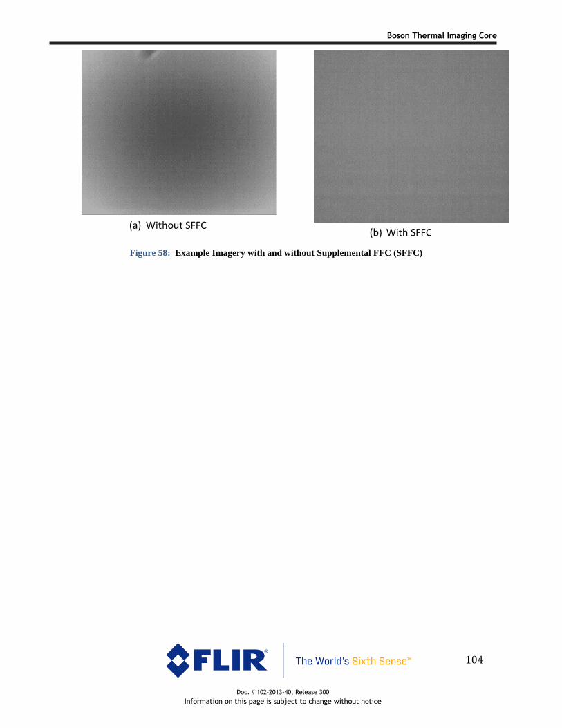
Boson Thermal Imaging Core
Doc. # 102-2013-40, Release 300
Information on this page is subject to change without notice
104
(a) Without SFFC
(b) With SFFC
Figure 58: Example Imagery with and without Supplemental FFC (SFFC)

Doc. # 102-2013-40, Release 300
Information on this page is subject to change without notice
F L I R B o s o n ® T h e r m a l I m a g i n g C o r e P r o d u c t D a t a s h e e t
105
12 Electrical Specifications
12.1 DC and Logic Level Specifications
Table 16: DC and Logic Levels
Parameter Description Min Typ Max Ripple,
p-p max
Units
3V3 Core Voltage (primary power for the Boson core)
3.14
See note 1
3.30 3.46 0.060 Volts
USB_VBUS USB Power 4.40 5.00 5.25 -- Volts
I_3V3 Primary supply current for Boson core
-- See note 2 560 / 1030
See note 3 n/a mA
I_VBUS Supply current for USB -- -- 0.130 n/a mA
Note(s)
1. 3V3 rise time from 0V to minimum voltage shall not exceed 1 msec.
2. Typical current varies with settings. See Section 12.2.
3. The first number shown is for the 320 configuration, the second for the 640 configuration. In either case, the value shown is during shutter actuation.
12.2 Power Consumption
Boson power consumption is dependent upon three primary variables:
• Camera operating temperature
• Whether the frame averager function is enabled (see Section 5.1)
• Whether the USB channel is streaming video (see Section 8.2.2)
Figure 59 shows typical power consumption of the 320 Release 2 configuration over the full operating temperature range with and without the frame averager enabled and with and without the USB channel streaming video. For reference, Figure 60 shows the same set of curves for the Release 1 configuration. As can be seen by comparing the two figures, upgrading a Release 1 camera to Release 2 software will result in a power savings between 130mW and 260 mW, depending upon temperature and use conditions.
Power consumption for the 640 Release 2 configuration is depicted in Figure 61. (There is no equivalent Release 1 configuration for Boson 640.)

Doc. # 102-2013-40, Release 300
Information on this page is subject to change without notice
106
Figure 59: Typical Power Variation of the 320 Release 2 Configuration over Temperature
Figure 60: Typical Power Variation of the 320 Release 1 Configuration over Temperature

Doc. # 102-2013-40, Release 300
Information on this page is subject to change without notice
F L I R B o s o n ® T h e r m a l I m a g i n g C o r e P r o d u c t D a t a s h e e t
107
Figure 61: Typical Power Variation of the 640 Release 2 Configuration over Temperature
NOTE: The power curves shown in the figures above are average values. The instantaneous
power when the camera’s internal shutter is actuated will be higher. For the 320 configuration,
the current draw increases by as much as 315 mA during a shutter event, and for the 640
configuration, the increase is as much as 550 mA. These values are included in the max. current
supply values listed in Table 16.
12.3 Absolute Maximum Ratings
Electrical stresses beyond those listed in Table 17 may cause permanent damage to the device. These are stress rating only, and functional operation of the device at these or any other conditions beyond those indicated under the recommended operating conditions listed in Table 16 is not implied. Exposure to absolute-maximum-rated conditions for extended periods of time may affect device reliability.
Table 17: Absolute Maximum Ratings
Parameter Absolute Maximum Rating

Doc. # 102-2013-40, Release 300
Information on this page is subject to change without notice
108
Core Voltage (3V3) 3.63V
USB VBUS 5.25V
Voltage on any GPIO pin 1.98V
Voltage on any USB signal pin 5.25V
Core temperature during operation 105C

Doc. # 102-2013-40, Release 300
Information on this page is subject to change without notice
F L I R B o s o n ® T h e r m a l I m a g i n g C o r e P r o d u c t D a t a s h e e t
109
13 Environmental Specifications
Environmental stresses beyond those listed in Table 18 may cause permanent damage to the
device. Exposure to absolute-maximum-rated conditions for extended periods of time may affect
device reliability.
Table 18: Environmental Specifications
Stress Maximum Rating
Operating Temperature Range1 -40° C to 80° C
Storage Temperature -50° C to 105° C
Altitude (pressure) 12 km altitude equivalent
Relative Humidity 93% non-condensing
Thermal Shock Air-to-air, between 20C and storage temp. extremes (i.e., 20° C to -50° C, -50° C to 20° C, 20C to 85C, 85C to 20C))
Mechanical Shock 250g, 1.5 msec
500g, 0.8 msec
1500 g, 0.5 msec
Vibration Transportation profile, 4.3 grms
Salt Fog2,3 HAR configs: unspecified
DLC configs: 240 hours per MIL-STD-810G
Method 509.4 IP Rating2 IP67 per IEC 60529
Abrasion3 HAR configs: MIL-C-675C (section 4.5.11) moderate abrasion
DLC configs: RSRE TS1888 Windscreen Wiper Test
ESD4 EN 61000-4-2 Level 4
• 8kV direct discharge
• 15 kV air-gap discharge
Note(s)
1. Temperature refers to that at the rear mounting surface of the camera
2. Salt fog and IP rating only applies to the portion of the lens assembly in front of the sealing surface (i.e.,
the o-ring groove on large lens configurations, the cylindrical portion of the lens flange for smaller-lens
configurations).
3. Most Boson lens assemblies have a high-durability AR (HAR) coating. The 92 deg (2.3mm) lens
configuration has a Diamond-Like Coating (DLC). See Section 10.
4. Proper ESD packaging and handling procedures are required to protect the Boson Core from ESD
Damage. Additionally, it is highly recommended for host electronics to incorporate the protection
circuitry shown in Section 4.2.

Doc. # 102-2013-40, Release 300
Information on this page is subject to change without notice
110
14 Compliance with Environmental Directives
Boson complies with the following directives and regulations:
■ Directive 2011/65/EC, “Restriction of the use of certain Hazardous Substances in electrical and electronic equipment (RoHS)”
■ Directive 2002/96/ EC, “Waste Electrical and Electronic Equipment (WEEE)”. ■ Regulation (EC) 1907/2006, “Registration, Evaluation, Authorization and Restriction of
Chemicals (REACH)
15 Reliability Section to be added in next release, pending life testing currently in progress.
16 Accessories A number of accessories have been designed for use with Boson. These are listed below and described in more detail in the sections to follow.
• Boson USB VPC Kit (421-0061-00)
• Boson USB / Analog Video Power Connector (VPC) Kit (421-0062-00)
• Boson Camera Link Accessory (250-0609-00)
• Boson Dev Board (250-0593-00)
• Boson Tripod Mount (261-2608-00)
• Boson Lens Focus Tool (421-2609-00)
16.1 USB VPC Kit The USB VPC kit, depicted in Figure 62, turns the Boson camera into a webcam. Power, digital video, and comm are all via USB2. The kit includes a 3-foot USB-A to USB-C cable.
16.2 USB / Analog VPC Kit The USB / Analog VPC kit, depicted in Figure 63, is identical to the USB VPC kit except that includes a custom 6-foot cable with a BNC pigtail providing an additional analog video signal (NTSC-compliant).

Doc. # 102-2013-40, Release 300
Information on this page is subject to change without notice
F L I R B o s o n ® T h e r m a l I m a g i n g C o r e P r o d u c t D a t a s h e e t
111
Figure 62: Boson VPC Kit (shown in conjunction with the Boson Tripod Accessory)
Figure 63: Boson VPC / Analog Kit (shown in conjunction with the Boson Tripod Accessory)
NOTE: Cable lengths shown in Figure 63 and Figure 62 are not to scale. Actual length is 0.9m
(3.0ft) for the VPC kit and 1.8m (6.0 ft) for the VPC / Analog kit.

Doc. # 102-2013-40, Release 300
Information on this page is subject to change without notice
112
16.3 Camera Link Accessory The Camera Link accessory, depicted in Figure 64, converts Boson’s CMOS video signal into a Camera-Link-compliant output, with physical interface via a standard SDR-26 receptacle. Communication and power to the Boson is provided via a standard USB-3 micro-B (Super Speed) receptacle. Note that a USB-2 micro-B cable is an acceptable alternative to a USB-3 micro-B cable for communication and power.
Figure 64: Boson Camera Link accessory
16.4 Boson Dev Board The Boson Development Board, shown in Figure 65, is intended to support the electronics developer integrating the Boson into an end system. It provides full access to the Boson 80-pin connector with a number of fan-out connectors:
• standard USB-3 micro-B (Super Speed) receptacle
• standard SDR-26 receptacle with Camera-Link compliant output
• SDIO card slot
• UART header
• I2C header
• SPI header
• Power jacks

Doc. # 102-2013-40, Release 300
Information on this page is subject to change without notice
F L I R B o s o n ® T h e r m a l I m a g i n g C o r e P r o d u c t D a t a s h e e t
113
Figure 65: Boson Dev Board (with Boson)
16.5 Tripod-Mount Accessory The Tripod-mount accessory, previously shown in Figure 63 and also shown in Figure 66, provides a means to mount a Boson assembly (or a Boson configured with either the VPC Accessory or the Camera Link Accessory) to a tripod via a standard 1/4-20 thread. It is designed to interface to the rear of the Boson via 4xM1.6 screws.
Figure 66: Boson Tripod-mount accessory

Doc. # 102-2013-40, Release 300
Information on this page is subject to change without notice
114
16.6 Focus-Tool Accessory The focus-tool accessory, shown in Figure 67, allows any FLIR Boson lens which cannot be focused by hand to be focused by engaging the appropriate slots on the lens barrel such that it can be rotated inside the lens flange. The focus tool has been properly sized such that no vignetting results when it engages the slots on the lens barrel. Note that lens configurations with focal length >25mm do not require a focus tool since focus is achieved by simply turning the outer barrel of the lens assembly by hand.
Figure 67: Boson Focus-tool accessory

Doc. # 102-2013-40, Release 300
Information on this page is subject to change without notice
F L I R B o s o n ® T h e r m a l I m a g i n g C o r e P r o d u c t D a t a s h e e t
115
17 References
17.1 FLIR Documents
Document Number
Document Title
102-2013-01 Boson Quick-Start Guide
102-2013-43 Boson Software IDD
Various Mechanical Interface Description Drawing (varies by part number)
102-2013-100-XX Various Boson Application Notes
17.2 External Documents
Document Number
Document Title
Directive 2011/65/EC Restriction of the use of certain Hazardous Substances in electrical and electronic equipment (RoHS)
IEC 61000-4-2 Electromagnetic Compatibility (EMC) Testing and Measurement Techniques, ESD Immunity Test
IEC 60529 Degrees of protection provided by enclosures (IP Code)
JESD22-A115C Electrostatic Discharge Sensitivity Testing, Machine Model (MM)
JESD22-C101E Field-Induced Charged-Device Model Test Method for Electrostatic Discharge Withstand Thresholds of Microelectronic Components
JEDEC JS-001-2012 Electrostatic Discharge Sensitivity Testing, Human Body Model (HBM) -- Component Testing
MIL-C-675C Coating of Glass Optical Elements (Anti-reflection)
MIL-STD-810G DoD Test Method Standard: Environmental Engineering Considerations and Laboratory Tests

Doc. # 102-2013-40, Release 300
Information on this page is subject to change without notice
116
17.3 Abbreviations / Acronyms
Abbreviation/ Acronym
Components
4CC Four Character Code
ACE Adaptive Contrast Enhancement
AGC Automatic Gain Control
API Application Program Interface
AR Anti-Reflection
CCI Command and Control Interface
CDM Charged-Device Model
CMOS Complementary Metal-Oxide-Semiconductor
CRC Cyclical Redundancy Check
DDE Digital Detail Enhancement
DVE Driver’s Vision Enhancer
EMC Electromagnetic Compatibility
ESD Electrostatic Damage
FFC Flat Field Correction
FOV Field of View
FPA Focal Plane Array
FPN Fixed Pattern Noise
GPIO General Purpose Input / Output
GUI Graphical User Interface
HBM Human Body Model
HEQ Histogram Equalization
HFOV Horizontal Field of View
I2C Inter-Integrated Circuit
IDD Interface Description Drawing / Document
IIR Infinite Impulse Response
IP Ingress Protection (also Intellectual Property)
LUT Look-Up Table
LWIR Long Wave Infrared
MISO Master In / Slave Out
MM Machine Model
MOSI Master-Out / Slave In

Doc. # 102-2013-40, Release 300
Information on this page is subject to change without notice
F L I R B o s o n ® T h e r m a l I m a g i n g C o r e P r o d u c t D a t a s h e e t
117
MTBF Mean Time Between Failure
MTF Modulation Transfer Function
NETD Noise Equivalent Temperature Difference
NFOV Narrow Field of View
NUC Non-Uniformity Correction
NVFFC Nonvolatile FFC
QVGA Quarter VGA, Quarter Video Graphic Array
REACH Registration, Evaluation, Authorization, and Restriction of CHemicals
RGB Red, Green, Blue (color space used to represent digital video)
RoHS Reduction of Hazardous Substances
ROI Region of Interest
ROIC Readout Integrated Circuit
UART Universal Asynchronous Receiver / Transmitter
USB Universal Serial Bus
UVC USB Video-Device Class
SBNUC Scene-Based Non-Uniformity Correction
SDIO Secure Digital Input Output
SDK Software Developers’ Kit
SFFC Supplemental FFC
SNR Signal-to-Noise Ratio
SSN Silent Shutterless NUC
SWAP Size, Weight, and Power
UAV Unmanned Aerial Vehicle
USB Universal Serial Bus
TBD To Be Determined
TCR Temperature Coefficient of Resistance
SoC System on a Chip
VGA Video Graphic Array
VOx Vanadium Oxide
WEEE Waste Electrical and Electronic Equipment
WFOV Wide Field of View
YCrCb Luma, Red Chrominance, Blue Chrominance (color space used to represent digital video)

Doc. # 102-2013-40, Release 300
Information on this page is subject to change without notice
118
© FLIR Commercial Systems, 2018. All rights reserved worldwide. No parts of this manual, in whole or in part, may be copied, photocopied, translated, or transmitted to any electronic medium or machine readable form without the prior written permission of FLIR Commercial Systems Names and m a r k s appearing on the p r o d u c t s herein are either registered trademarks or trademarks of FLIR Commercial Systems and/or its subsidiaries. All other trademarks, trade names, or company names referenced herein are used for identification only and a re the property of their respective owners. This product is protected by patents, design patents, patents pending, or design patents pending. Croscore fonts are copyright 2010 by Google Corporation and are used under authority of the Apache License, Version 2.0. Information about this license can be found at:
http://www.apache.org/licenses/LICENSE-2.0 If you have q u e s t i o n s that are not covered in this ma nua l contact FLIR Commercial Systems Customer Support ([email protected]) for additional information. Contact Customer Support for questions related to the use of open-source software in this product. And contact Customer Support prior t o returning a camera which is in need of service. This documentation and the requirements specified herein are subject to change without notice.
This equipment must be disposed of as electronic waste. Contact your nearest FLIR Commercial Systems, Inc. representative for instructions on how to return the p r o d u c t to FLIR for proper disposal.
FCC Notice. This device is a subassembly designed for incorporation into other products in order to provide an infrared camera function. It is not an end-product fit for consumer use. When incorporated into a host device, the end-product will generate, use, and radiate radio frequency energy that may cause radio interference. As such, the end-product incorporating this subassembly must be tested and approved under the rules of the Federal Communications Commission (FCC) before the end-product may be offered for sale or lease, advertised, imported, sold, or leased in the United States. The FCC regulations are designed to provide reasonable protection against interference to radio communications. See 47 C.F.R. §§ 2.803 and 15.1 et seq. Industry Canada Notice. This device is a subassembly designed for incorporation into other products in order to provide an infrared camera function. It is not an end-product fit for consumer use. When incorporated into a host device, the end-product will generate, use, and radiate radio frequency energy that may cause radio interference. As such, the end-product incorporating this subassembly must be tested for compliance with the Interference-Causing Equipment Standard, Digital Apparatus, ICES-003, of Industry Canada before the product incorporating this device may be: manufactured or offered for sale or lease, imported, distributed, sold, or leased in Canada. Avis d’Industrie Canada. Cet appareil est un sous-ensemble conçu pour être intégré à un autre produit afin de fournir une fonction de caméra infrarouge. Ce n’est pas un produit final destiné aux consommateurs. Une fois intégré à un dispositif hôte, le produit final va générer, utiliser et émettre de l’énergie radiofréquence qui pourrait provoquer de l’interférence radio . En tant que tel, le produit final intégrant ce sous-ensemble doit être testé pour en vérifier la conformité avec la Norme sur le matériel brouilleur pour les appareils numériques (NMB-003) d’Industrie Canada avant que le produit intégrant ce dispositif puisse être fabriqué, mis en vente ou en location, importé, distribué, vendu ou loué au Canada. EU Notice. This device is a subassembly or component intended only for product evaluation, development or incorporation into other products in order to provide an infrared camera function. It is not a finished end-product fit for general consumer use. Persons handling this device must have appropriate electronics training and observe good engineering practice standards. As such, this product does not fall within the scope of the European Union (EU) directives regarding electromagnetic compatibility (EMC). Any end-product intended for general consumer use that incorporates this device must be tested in accordance and comply with all applicable EU EMC and other relevant directives.