Black Phosphorus and Phosphorene for Device...
28
Black Phosphorus and Phosphorene for Device Applications Peide (Peter) Ye School of Electrical and Computer Engineering and Birck Nanotechnology Center, Purdue University NSF US-EU Workshop on 4/23/2015
Transcript of Black Phosphorus and Phosphorene for Device...
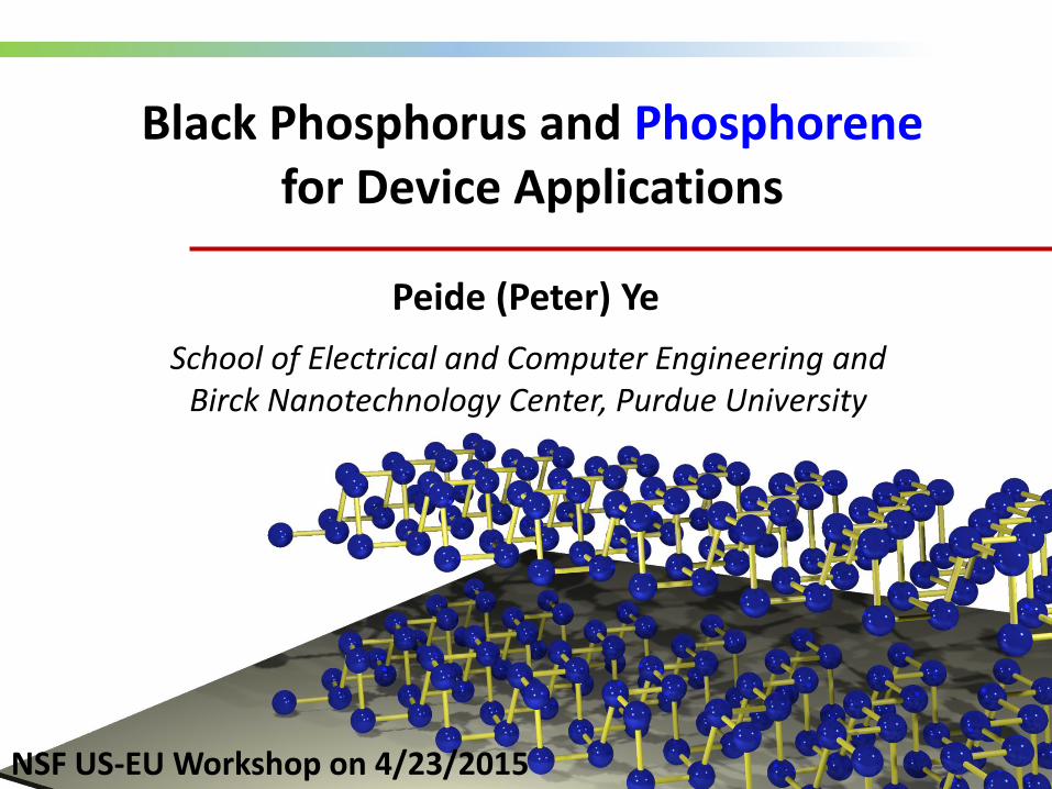
Black Phosphorus and Phosphorene for Device Applications
Peide (Peter) Ye
School of Electrical and Computer Engineering and Birck Nanotechnology Center Purdue University
NSF US-EU Workshop on 4232015
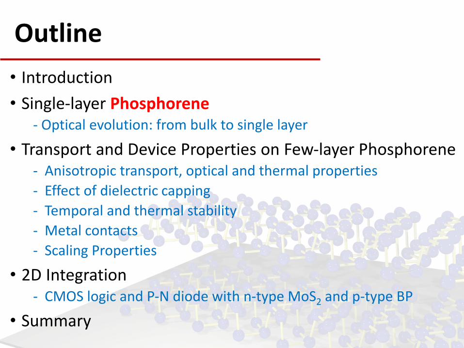
Outline
bull Introduction
bull Single-layer Phosphorene - Optical evolution from bulk to single layer
bull Transport and Device Properties on Few-layer Phosphorene - Anisotropic transport optical and thermal properties
- Effect of dielectric capping
- Temporal and thermal stability
- Metal contacts
- Scaling Properties
bull 2D Integration - CMOS logic and P-N diode with n-type MoS2 and p-type BP
bull Summary
White Phosphorus
Red Phosphorus
Explosion
Safety Matches
Allotropes of Phosphorus
Black Phosphorus Electronics
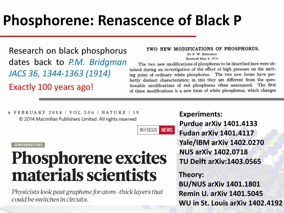
Phosphorene Renascence of Black P
Research on black phosphorus dates back to PM Bridgman JACS 36 1344-1363 (1914)
Exactly 100 years ago
Experiments Purdue arXiv 14014133 Fudan arXiv 14014117 YaleIBM arXiv 14020270 NUS arXiv 14020718 TU Delft arXiv14030565
Theory BUNUS arXiv 14011801 Remin U arXiv 14015045 WU in St Louis arXiv 14024192
DFT Band Structure
Single layer black phosphorus ndash ldquoPhosphorenerdquo
Band Structure of Phosphorene In collaborations with Prof Tomanek (MSU)
055 nm
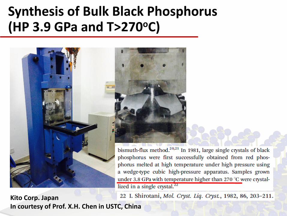
Kito Corp Japan In courtesy of Prof XH Chen in USTC China
Synthesis of Bulk Black Phosphorus (HP 39 GPa and Tgt270oC)
S Lange et al Inorg Chem 46 4028 2007 M Kopf et al arXiv 14067275
Synthesis of Black P using SnSnI4
300 350 400 450 500
Inte
nsity
Raman shift
Purdue Yersquos group
Single-layer Phosphorene
1 μm
T = 085 nm
13 14 15 16 17 18
0
100
200
300
400
500
600
Single-Layer
Phosphorene
Inte
nsity (
au
)
Energy (eV)
Bulk BP
330 360 390 420 450 480
Bulk
2L
B2gA2
g
Ram
an
Inte
nsity
Raman Shift (cm-1)
A1g
1L
Atomic Force Microscopy Photoluminescence
Raman Spectra
In collaborations with Prof Xu (Purdue)
arXiv 1407 0502 Zhang et al
Australian National University
Phosphorene Transistors
-30 -20 -10 0 10 20 30
10-4
10-3
10-2
10-1
100
101
102
103
Dra
in C
urr
en
t (m
Am
m) Vds=001V
Vds=05V
Dra
in C
urr
en
t (m
Am
m)
Back Gate Voltage (V)
00
05
10
15
T=300 K
FE=286cm2Vs
-20 -15 -10 -05 00
0
50
100
150
200
30V
0V
Dra
in C
urr
en
t (m
Am
m)
Drain Voltage (V)
-30V Phosphorene p-type FET
Lch=1m
Drain current 194 mAmm Field Effect Mobility 286 cm2Vs
Phosphorene ~5 nm thick
90 nm SiO2
TiAu contact
1 μm gate length
Global gate modulation
Field-effect Mobility
Side View
Top View
measympmhasymp03m0 mhasymp83 m0 measymp26 m0
Anisotropic Effective Mass
0 5 10 15 20 25 30
0
50
100
150
200
250
300
Mo
bili
ty (
cm
2Vs
)
Thickness (nm)
Anisotropic Field-effect Mobility
bull Devices are randomly distributed of crystal orientations H Liu et al ACS Nano March 2014
Theoretical work K-T Lam et al EDL 35 963 2014 K Gong et al PBB 90 125441 2014
Vds=-05 V
Vds=-005 V
0 60 120 180 240 300 360
80
100
120
140
160
Dra
in C
urr
ent (m
Am
m)
Angle (degrees)
032
036
040
044
048
Gm
(m
Sm
m)
0
45 o
o
An anisotropic transport of over 50 difference in conductance is observed
Anisotropic Transport
120590=120590119909119909sin2(120579 minus 1205790) + 120590119910119910cos
2(120579 minus 1205790
H Liu et al ACS Nano March 2014 Also Xia et al arXiv 14020270
Anisotropic Optical Properties
Z Luo et al arXiv 150306167 2015 Also F Xia et al Nature Communication 2014
A Favron et al arXiv 14080345
In collaborations with Prof Xianfan Xu (Purdue)
Anisotropic Thermal Properties
In collaborations with Xianfan Xursquos group at Purdue
Z Luo et al arXiv 150306167 2015
Theoretical work reported by R Fei et al NL 146393 2014
B Liao et al arXiv 14104242 G Qin et al arXiv 14090279
Stability of Phosphorene in ambient
After device fabrication After 48 hours in ambient
A Favron et al arXiv 14080345
(1) O2 H2O light accelerate the degrade process (2) Our XPS studies show that H2O is critical phosphorus acid could be formed Y Deng et al APS March Meeting 2015
Solutions (1) Atomic-Layer-Deposited (ALD) capping layer (2) Other organic polymer type capping layer (3) h-BNphosphoreneh-BN heterostructure
JO Island et al 2D Materials 2015
ALD Dielectric Capping
φbe
φbh
φbe
φbh
+ +
wo Al2O3 capping w Al2O3 capping
EC
EV EF
-30 -20 -10 0 10 20 30
10-5
10-4
10-3
10-2
10-1
100
101 16 nm Al2O3 on top
Back gate modulation
Vds= -05 V
Vds=-001 V
Dra
in C
urr
en
t (m
Am
m)
Back Gate Voltage (V)
~x103
-30 -20 -10 0 10 20 30
10-4
10-3
10-2
10-1
100
101
102
Dra
in C
urr
ent (m
Am
m)
Vds=-001 V
Gate Voltage (V)
p=956 cm2Vs
Vds=-05 V
0
20
40
60
80
100
H Liu et al IEEE EDL July 2014 Low Temperature ALD (150oC or 200oC)
ALD Dielectric Capping
JD Wood et al Nano Letters 14 6964 2014
H Wang et al Nano Letters 14 6424 2014
J-S Kim et al arXiv 14120355
h-BNphosphoreneh-BN Capping
L Li et al arXiv 14116572 N Gillgren et al 2D Materials 2 1001 2015
Similar work also reported V Tayari et al arXiv14120259 X Chen et al arXiv 14121357 A Avsar et al arXiv 14121191 RA Doganov et al arXiv 14121274 Y Cao et al arXiv 150203755
Metal Contacts
Ni-Contact Ambipolar Pd-Contact P-type
-40 -20 0 20 4010
-2
10-1
100
101
102
Vds= 001 V
Vds= 05 V
Dra
in C
urr
en
t (m
Am
m)
Back Gate Voltage (V)
FE
=1705 cm2Vs
Ni
0
5
10
15
20
25
-40 -20 0 20 40
10-2
10-1
100
101
102
Vds= 001 V
Vds= 05 V
Dra
in C
urr
en
t (m
Am
m)
Back Gate Voltage (V)
FE
=1865 cm2Vs
Pd
0
5
10
15
20
25
30
35
Band edge alignment
φbe
φbh
EC
EV EF Rc=15-20 Ωmiddotmm
N-type and P-type Doping Technique on Phosphorene is under development
-40 -20 0 20 40
100
101
102
P-type Pd-contact
BP Transistors
Vds = 05 V
L = 100 nm
L = 200 nm
L = 500 nm
L = 2 m
Dra
in C
urr
ent (m
Am
m)
Back Gate Voltage (V)-40 -20 0 20 40
100
101
102
Ambipolar Ni-contact
BP Transistors
Vds = 05 V
L = 100 nm
L = 200 nm
L = 500 nm
L = 2 m
Dra
in C
urr
en
t (m
Am
m)
Back Gate Voltage (V)
Scaling Properties
Long-channel Short-channel
Enhanced Ambipolarity
Ni-Contact Pd-Contact
Фse
Vds
Фse
Vds Reduced SB width
Y Du et al ACS Nano 2014 10 nm Back-gated Phosphorene FET is under development
2D CMOS Logic
VDD
VOUT
GND
VIN
VDD
GND
VIN VOUT
Phosphorene PMOS
MoS2 NMOS
SiSiO2 substrate
Al2O3 dielectric
TiAu contacts
TiAu metal gates
H Liu et al ACS Nano March 2014
2D CMOS Logic - VTC
-10 -8 -6 -4 -2
00
02
04
06
08
10
Vo
ut (V
)
Vin (V)
VDD=1V
00
03
06
09
12
15
Gain
2D Hetero-structure
Y Deng et al ACS Nano July 2014
BP Homo-junction Y Deng et al IEDM 2014 Also M Buscema et al Nano Letters 2014
Photo-response of BPMoS2 pn diode
Maximum photo-detection responsivity of 418 mAW
PV energy conversion with an external quantum efficiency of 03
Energy harvesting of BPMoS2 pn diode
Other phosphorene work on photonic applications
M Buscema et al Nano Letters 2014
M Engel et al Nano Letters 2014
T Low et al PRB 90 081408 2014
Summary
bull Single-layer phosphorene is demonstrated first time with strong PL peak and Raman shift
bull High performance transistor are achieved on few-layer phosphorene crystals An on-current of 194 mAmm and field-effect hole mobility of 286 cm2Vs are obtained
bull Anisotropic transport is observed at the orthogonal direction and attributed to different effective mass
bull Dielectric capping temporalthermal stability metal contacts and scaling properties are investigated with phosphorene transistors
bull 2D CMOS inverter and 2D p-n diode are demonstrated with n-type MoS2 p-type phosphorene
Acknowledgement
Prof Jun Lou Prof Pulickel Ajayan Mr Sina Najmaei
Prof David Tomanek Mr Zhen Zhu
Han Liu (Intel) Adam Neal (AFRL) Yuchen Du Yexin Deng Lingming Yang Zhe Luo Prof X Xu
Prof James CM Hwang Mr Xi Luo Yaghoob Rahbarihagh
Acquiring Black P from vendors
$100 in ebay by the end of 2012 $800 similar quantity
a factor of 8 increases
Outline
bull Introduction
bull Single-layer Phosphorene - Optical evolution from bulk to single layer
bull Transport and Device Properties on Few-layer Phosphorene - Anisotropic transport optical and thermal properties
- Effect of dielectric capping
- Temporal and thermal stability
- Metal contacts
- Scaling Properties
bull 2D Integration - CMOS logic and P-N diode with n-type MoS2 and p-type BP
bull Summary
White Phosphorus
Red Phosphorus
Explosion
Safety Matches
Allotropes of Phosphorus
Black Phosphorus Electronics
Phosphorene Renascence of Black P
Research on black phosphorus dates back to PM Bridgman JACS 36 1344-1363 (1914)
Exactly 100 years ago
Experiments Purdue arXiv 14014133 Fudan arXiv 14014117 YaleIBM arXiv 14020270 NUS arXiv 14020718 TU Delft arXiv14030565
Theory BUNUS arXiv 14011801 Remin U arXiv 14015045 WU in St Louis arXiv 14024192
DFT Band Structure
Single layer black phosphorus ndash ldquoPhosphorenerdquo
Band Structure of Phosphorene In collaborations with Prof Tomanek (MSU)
055 nm
Kito Corp Japan In courtesy of Prof XH Chen in USTC China
Synthesis of Bulk Black Phosphorus (HP 39 GPa and Tgt270oC)
S Lange et al Inorg Chem 46 4028 2007 M Kopf et al arXiv 14067275
Synthesis of Black P using SnSnI4
300 350 400 450 500
Inte
nsity
Raman shift
Purdue Yersquos group
Single-layer Phosphorene
1 μm
T = 085 nm
13 14 15 16 17 18
0
100
200
300
400
500
600
Single-Layer
Phosphorene
Inte
nsity (
au
)
Energy (eV)
Bulk BP
330 360 390 420 450 480
Bulk
2L
B2gA2
g
Ram
an
Inte
nsity
Raman Shift (cm-1)
A1g
1L
Atomic Force Microscopy Photoluminescence
Raman Spectra
In collaborations with Prof Xu (Purdue)
arXiv 1407 0502 Zhang et al
Australian National University
Phosphorene Transistors
-30 -20 -10 0 10 20 30
10-4
10-3
10-2
10-1
100
101
102
103
Dra
in C
urr
en
t (m
Am
m) Vds=001V
Vds=05V
Dra
in C
urr
en
t (m
Am
m)
Back Gate Voltage (V)
00
05
10
15
T=300 K
FE=286cm2Vs
-20 -15 -10 -05 00
0
50
100
150
200
30V
0V
Dra
in C
urr
en
t (m
Am
m)
Drain Voltage (V)
-30V Phosphorene p-type FET
Lch=1m
Drain current 194 mAmm Field Effect Mobility 286 cm2Vs
Phosphorene ~5 nm thick
90 nm SiO2
TiAu contact
1 μm gate length
Global gate modulation
Field-effect Mobility
Side View
Top View
measympmhasymp03m0 mhasymp83 m0 measymp26 m0
Anisotropic Effective Mass
0 5 10 15 20 25 30
0
50
100
150
200
250
300
Mo
bili
ty (
cm
2Vs
)
Thickness (nm)
Anisotropic Field-effect Mobility
bull Devices are randomly distributed of crystal orientations H Liu et al ACS Nano March 2014
Theoretical work K-T Lam et al EDL 35 963 2014 K Gong et al PBB 90 125441 2014
Vds=-05 V
Vds=-005 V
0 60 120 180 240 300 360
80
100
120
140
160
Dra
in C
urr
ent (m
Am
m)
Angle (degrees)
032
036
040
044
048
Gm
(m
Sm
m)
0
45 o
o
An anisotropic transport of over 50 difference in conductance is observed
Anisotropic Transport
120590=120590119909119909sin2(120579 minus 1205790) + 120590119910119910cos
2(120579 minus 1205790
H Liu et al ACS Nano March 2014 Also Xia et al arXiv 14020270
Anisotropic Optical Properties
Z Luo et al arXiv 150306167 2015 Also F Xia et al Nature Communication 2014
A Favron et al arXiv 14080345
In collaborations with Prof Xianfan Xu (Purdue)
Anisotropic Thermal Properties
In collaborations with Xianfan Xursquos group at Purdue
Z Luo et al arXiv 150306167 2015
Theoretical work reported by R Fei et al NL 146393 2014
B Liao et al arXiv 14104242 G Qin et al arXiv 14090279
Stability of Phosphorene in ambient
After device fabrication After 48 hours in ambient
A Favron et al arXiv 14080345
(1) O2 H2O light accelerate the degrade process (2) Our XPS studies show that H2O is critical phosphorus acid could be formed Y Deng et al APS March Meeting 2015
Solutions (1) Atomic-Layer-Deposited (ALD) capping layer (2) Other organic polymer type capping layer (3) h-BNphosphoreneh-BN heterostructure
JO Island et al 2D Materials 2015
ALD Dielectric Capping
φbe
φbh
φbe
φbh
+ +
wo Al2O3 capping w Al2O3 capping
EC
EV EF
-30 -20 -10 0 10 20 30
10-5
10-4
10-3
10-2
10-1
100
101 16 nm Al2O3 on top
Back gate modulation
Vds= -05 V
Vds=-001 V
Dra
in C
urr
en
t (m
Am
m)
Back Gate Voltage (V)
~x103
-30 -20 -10 0 10 20 30
10-4
10-3
10-2
10-1
100
101
102
Dra
in C
urr
ent (m
Am
m)
Vds=-001 V
Gate Voltage (V)
p=956 cm2Vs
Vds=-05 V
0
20
40
60
80
100
H Liu et al IEEE EDL July 2014 Low Temperature ALD (150oC or 200oC)
ALD Dielectric Capping
JD Wood et al Nano Letters 14 6964 2014
H Wang et al Nano Letters 14 6424 2014
J-S Kim et al arXiv 14120355
h-BNphosphoreneh-BN Capping
L Li et al arXiv 14116572 N Gillgren et al 2D Materials 2 1001 2015
Similar work also reported V Tayari et al arXiv14120259 X Chen et al arXiv 14121357 A Avsar et al arXiv 14121191 RA Doganov et al arXiv 14121274 Y Cao et al arXiv 150203755
Metal Contacts
Ni-Contact Ambipolar Pd-Contact P-type
-40 -20 0 20 4010
-2
10-1
100
101
102
Vds= 001 V
Vds= 05 V
Dra
in C
urr
en
t (m
Am
m)
Back Gate Voltage (V)
FE
=1705 cm2Vs
Ni
0
5
10
15
20
25
-40 -20 0 20 40
10-2
10-1
100
101
102
Vds= 001 V
Vds= 05 V
Dra
in C
urr
en
t (m
Am
m)
Back Gate Voltage (V)
FE
=1865 cm2Vs
Pd
0
5
10
15
20
25
30
35
Band edge alignment
φbe
φbh
EC
EV EF Rc=15-20 Ωmiddotmm
N-type and P-type Doping Technique on Phosphorene is under development
-40 -20 0 20 40
100
101
102
P-type Pd-contact
BP Transistors
Vds = 05 V
L = 100 nm
L = 200 nm
L = 500 nm
L = 2 m
Dra
in C
urr
ent (m
Am
m)
Back Gate Voltage (V)-40 -20 0 20 40
100
101
102
Ambipolar Ni-contact
BP Transistors
Vds = 05 V
L = 100 nm
L = 200 nm
L = 500 nm
L = 2 m
Dra
in C
urr
en
t (m
Am
m)
Back Gate Voltage (V)
Scaling Properties
Long-channel Short-channel
Enhanced Ambipolarity
Ni-Contact Pd-Contact
Фse
Vds
Фse
Vds Reduced SB width
Y Du et al ACS Nano 2014 10 nm Back-gated Phosphorene FET is under development
2D CMOS Logic
VDD
VOUT
GND
VIN
VDD
GND
VIN VOUT
Phosphorene PMOS
MoS2 NMOS
SiSiO2 substrate
Al2O3 dielectric
TiAu contacts
TiAu metal gates
H Liu et al ACS Nano March 2014
2D CMOS Logic - VTC
-10 -8 -6 -4 -2
00
02
04
06
08
10
Vo
ut (V
)
Vin (V)
VDD=1V
00
03
06
09
12
15
Gain
2D Hetero-structure
Y Deng et al ACS Nano July 2014
BP Homo-junction Y Deng et al IEDM 2014 Also M Buscema et al Nano Letters 2014
Photo-response of BPMoS2 pn diode
Maximum photo-detection responsivity of 418 mAW
PV energy conversion with an external quantum efficiency of 03
Energy harvesting of BPMoS2 pn diode
Other phosphorene work on photonic applications
M Buscema et al Nano Letters 2014
M Engel et al Nano Letters 2014
T Low et al PRB 90 081408 2014
Summary
bull Single-layer phosphorene is demonstrated first time with strong PL peak and Raman shift
bull High performance transistor are achieved on few-layer phosphorene crystals An on-current of 194 mAmm and field-effect hole mobility of 286 cm2Vs are obtained
bull Anisotropic transport is observed at the orthogonal direction and attributed to different effective mass
bull Dielectric capping temporalthermal stability metal contacts and scaling properties are investigated with phosphorene transistors
bull 2D CMOS inverter and 2D p-n diode are demonstrated with n-type MoS2 p-type phosphorene
Acknowledgement
Prof Jun Lou Prof Pulickel Ajayan Mr Sina Najmaei
Prof David Tomanek Mr Zhen Zhu
Han Liu (Intel) Adam Neal (AFRL) Yuchen Du Yexin Deng Lingming Yang Zhe Luo Prof X Xu
Prof James CM Hwang Mr Xi Luo Yaghoob Rahbarihagh
Acquiring Black P from vendors
$100 in ebay by the end of 2012 $800 similar quantity
a factor of 8 increases
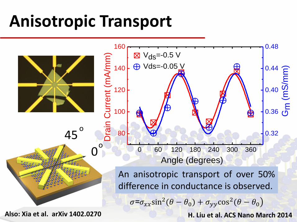
Vds=-05 V
Vds=-005 V
0 60 120 180 240 300 360
80
100
120
140
160
Dra
in C
urr
ent (m
Am
m)
Angle (degrees)
032
036
040
044
048
Gm
(m
Sm
m)
0
45 o
o
An anisotropic transport of over 50 difference in conductance is observed
Anisotropic Transport
120590=120590119909119909sin2(120579 minus 1205790) + 120590119910119910cos
2(120579 minus 1205790
H Liu et al ACS Nano March 2014 Also Xia et al arXiv 14020270
Anisotropic Optical Properties
Z Luo et al arXiv 150306167 2015 Also F Xia et al Nature Communication 2014
A Favron et al arXiv 14080345
In collaborations with Prof Xianfan Xu (Purdue)
Anisotropic Thermal Properties
In collaborations with Xianfan Xursquos group at Purdue
Z Luo et al arXiv 150306167 2015
Theoretical work reported by R Fei et al NL 146393 2014
B Liao et al arXiv 14104242 G Qin et al arXiv 14090279
Stability of Phosphorene in ambient
After device fabrication After 48 hours in ambient
A Favron et al arXiv 14080345
(1) O2 H2O light accelerate the degrade process (2) Our XPS studies show that H2O is critical phosphorus acid could be formed Y Deng et al APS March Meeting 2015
Solutions (1) Atomic-Layer-Deposited (ALD) capping layer (2) Other organic polymer type capping layer (3) h-BNphosphoreneh-BN heterostructure
JO Island et al 2D Materials 2015
ALD Dielectric Capping
φbe
φbh
φbe
φbh
+ +
wo Al2O3 capping w Al2O3 capping
EC
EV EF
-30 -20 -10 0 10 20 30
10-5
10-4
10-3
10-2
10-1
100
101 16 nm Al2O3 on top
Back gate modulation
Vds= -05 V
Vds=-001 V
Dra
in C
urr
en
t (m
Am
m)
Back Gate Voltage (V)
~x103
-30 -20 -10 0 10 20 30
10-4
10-3
10-2
10-1
100
101
102
Dra
in C
urr
ent (m
Am
m)
Vds=-001 V
Gate Voltage (V)
p=956 cm2Vs
Vds=-05 V
0
20
40
60
80
100
H Liu et al IEEE EDL July 2014 Low Temperature ALD (150oC or 200oC)
ALD Dielectric Capping
JD Wood et al Nano Letters 14 6964 2014
H Wang et al Nano Letters 14 6424 2014
J-S Kim et al arXiv 14120355
h-BNphosphoreneh-BN Capping
L Li et al arXiv 14116572 N Gillgren et al 2D Materials 2 1001 2015
Similar work also reported V Tayari et al arXiv14120259 X Chen et al arXiv 14121357 A Avsar et al arXiv 14121191 RA Doganov et al arXiv 14121274 Y Cao et al arXiv 150203755
Metal Contacts
Ni-Contact Ambipolar Pd-Contact P-type
-40 -20 0 20 4010
-2
10-1
100
101
102
Vds= 001 V
Vds= 05 V
Dra
in C
urr
en
t (m
Am
m)
Back Gate Voltage (V)
FE
=1705 cm2Vs
Ni
0
5
10
15
20
25
-40 -20 0 20 40
10-2
10-1
100
101
102
Vds= 001 V
Vds= 05 V
Dra
in C
urr
en
t (m
Am
m)
Back Gate Voltage (V)
FE
=1865 cm2Vs
Pd
0
5
10
15
20
25
30
35
Band edge alignment
φbe
φbh
EC
EV EF Rc=15-20 Ωmiddotmm
N-type and P-type Doping Technique on Phosphorene is under development
-40 -20 0 20 40
100
101
102
P-type Pd-contact
BP Transistors
Vds = 05 V
L = 100 nm
L = 200 nm
L = 500 nm
L = 2 m
Dra
in C
urr
ent (m
Am
m)
Back Gate Voltage (V)-40 -20 0 20 40
100
101
102
Ambipolar Ni-contact
BP Transistors
Vds = 05 V
L = 100 nm
L = 200 nm
L = 500 nm
L = 2 m
Dra
in C
urr
en
t (m
Am
m)
Back Gate Voltage (V)
Scaling Properties
Long-channel Short-channel
Enhanced Ambipolarity
Ni-Contact Pd-Contact
Фse
Vds
Фse
Vds Reduced SB width
Y Du et al ACS Nano 2014 10 nm Back-gated Phosphorene FET is under development
2D CMOS Logic
VDD
VOUT
GND
VIN
VDD
GND
VIN VOUT
Phosphorene PMOS
MoS2 NMOS
SiSiO2 substrate
Al2O3 dielectric
TiAu contacts
TiAu metal gates
H Liu et al ACS Nano March 2014
2D CMOS Logic - VTC
-10 -8 -6 -4 -2
00
02
04
06
08
10
Vo
ut (V
)
Vin (V)
VDD=1V
00
03
06
09
12
15
Gain
2D Hetero-structure
Y Deng et al ACS Nano July 2014
BP Homo-junction Y Deng et al IEDM 2014 Also M Buscema et al Nano Letters 2014
Photo-response of BPMoS2 pn diode
Maximum photo-detection responsivity of 418 mAW
PV energy conversion with an external quantum efficiency of 03
Energy harvesting of BPMoS2 pn diode
Other phosphorene work on photonic applications
M Buscema et al Nano Letters 2014
M Engel et al Nano Letters 2014
T Low et al PRB 90 081408 2014
Summary
bull Single-layer phosphorene is demonstrated first time with strong PL peak and Raman shift
bull High performance transistor are achieved on few-layer phosphorene crystals An on-current of 194 mAmm and field-effect hole mobility of 286 cm2Vs are obtained
bull Anisotropic transport is observed at the orthogonal direction and attributed to different effective mass
bull Dielectric capping temporalthermal stability metal contacts and scaling properties are investigated with phosphorene transistors
bull 2D CMOS inverter and 2D p-n diode are demonstrated with n-type MoS2 p-type phosphorene
Acknowledgement
Prof Jun Lou Prof Pulickel Ajayan Mr Sina Najmaei
Prof David Tomanek Mr Zhen Zhu
Han Liu (Intel) Adam Neal (AFRL) Yuchen Du Yexin Deng Lingming Yang Zhe Luo Prof X Xu
Prof James CM Hwang Mr Xi Luo Yaghoob Rahbarihagh
Acquiring Black P from vendors
$100 in ebay by the end of 2012 $800 similar quantity
a factor of 8 increases

ALD Dielectric Capping
φbe
φbh
φbe
φbh
+ +
wo Al2O3 capping w Al2O3 capping
EC
EV EF
-30 -20 -10 0 10 20 30
10-5
10-4
10-3
10-2
10-1
100
101 16 nm Al2O3 on top
Back gate modulation
Vds= -05 V
Vds=-001 V
Dra
in C
urr
en
t (m
Am
m)
Back Gate Voltage (V)
~x103
-30 -20 -10 0 10 20 30
10-4
10-3
10-2
10-1
100
101
102
Dra
in C
urr
ent (m
Am
m)
Vds=-001 V
Gate Voltage (V)
p=956 cm2Vs
Vds=-05 V
0
20
40
60
80
100
H Liu et al IEEE EDL July 2014 Low Temperature ALD (150oC or 200oC)
ALD Dielectric Capping
JD Wood et al Nano Letters 14 6964 2014
H Wang et al Nano Letters 14 6424 2014
J-S Kim et al arXiv 14120355
h-BNphosphoreneh-BN Capping
L Li et al arXiv 14116572 N Gillgren et al 2D Materials 2 1001 2015
Similar work also reported V Tayari et al arXiv14120259 X Chen et al arXiv 14121357 A Avsar et al arXiv 14121191 RA Doganov et al arXiv 14121274 Y Cao et al arXiv 150203755
Metal Contacts
Ni-Contact Ambipolar Pd-Contact P-type
-40 -20 0 20 4010
-2
10-1
100
101
102
Vds= 001 V
Vds= 05 V
Dra
in C
urr
en
t (m
Am
m)
Back Gate Voltage (V)
FE
=1705 cm2Vs
Ni
0
5
10
15
20
25
-40 -20 0 20 40
10-2
10-1
100
101
102
Vds= 001 V
Vds= 05 V
Dra
in C
urr
en
t (m
Am
m)
Back Gate Voltage (V)
FE
=1865 cm2Vs
Pd
0
5
10
15
20
25
30
35
Band edge alignment
φbe
φbh
EC
EV EF Rc=15-20 Ωmiddotmm
N-type and P-type Doping Technique on Phosphorene is under development
-40 -20 0 20 40
100
101
102
P-type Pd-contact
BP Transistors
Vds = 05 V
L = 100 nm
L = 200 nm
L = 500 nm
L = 2 m
Dra
in C
urr
ent (m
Am
m)
Back Gate Voltage (V)-40 -20 0 20 40
100
101
102
Ambipolar Ni-contact
BP Transistors
Vds = 05 V
L = 100 nm
L = 200 nm
L = 500 nm
L = 2 m
Dra
in C
urr
en
t (m
Am
m)
Back Gate Voltage (V)
Scaling Properties
Long-channel Short-channel
Enhanced Ambipolarity
Ni-Contact Pd-Contact
Фse
Vds
Фse
Vds Reduced SB width
Y Du et al ACS Nano 2014 10 nm Back-gated Phosphorene FET is under development
2D CMOS Logic
VDD
VOUT
GND
VIN
VDD
GND
VIN VOUT
Phosphorene PMOS
MoS2 NMOS
SiSiO2 substrate
Al2O3 dielectric
TiAu contacts
TiAu metal gates
H Liu et al ACS Nano March 2014
2D CMOS Logic - VTC
-10 -8 -6 -4 -2
00
02
04
06
08
10
Vo
ut (V
)
Vin (V)
VDD=1V
00
03
06
09
12
15
Gain
2D Hetero-structure
Y Deng et al ACS Nano July 2014
BP Homo-junction Y Deng et al IEDM 2014 Also M Buscema et al Nano Letters 2014
Photo-response of BPMoS2 pn diode
Maximum photo-detection responsivity of 418 mAW
PV energy conversion with an external quantum efficiency of 03
Energy harvesting of BPMoS2 pn diode
Other phosphorene work on photonic applications
M Buscema et al Nano Letters 2014
M Engel et al Nano Letters 2014
T Low et al PRB 90 081408 2014
Summary
bull Single-layer phosphorene is demonstrated first time with strong PL peak and Raman shift
bull High performance transistor are achieved on few-layer phosphorene crystals An on-current of 194 mAmm and field-effect hole mobility of 286 cm2Vs are obtained
bull Anisotropic transport is observed at the orthogonal direction and attributed to different effective mass
bull Dielectric capping temporalthermal stability metal contacts and scaling properties are investigated with phosphorene transistors
bull 2D CMOS inverter and 2D p-n diode are demonstrated with n-type MoS2 p-type phosphorene
Acknowledgement
Prof Jun Lou Prof Pulickel Ajayan Mr Sina Najmaei
Prof David Tomanek Mr Zhen Zhu
Han Liu (Intel) Adam Neal (AFRL) Yuchen Du Yexin Deng Lingming Yang Zhe Luo Prof X Xu
Prof James CM Hwang Mr Xi Luo Yaghoob Rahbarihagh
Acquiring Black P from vendors
$100 in ebay by the end of 2012 $800 similar quantity
a factor of 8 increases
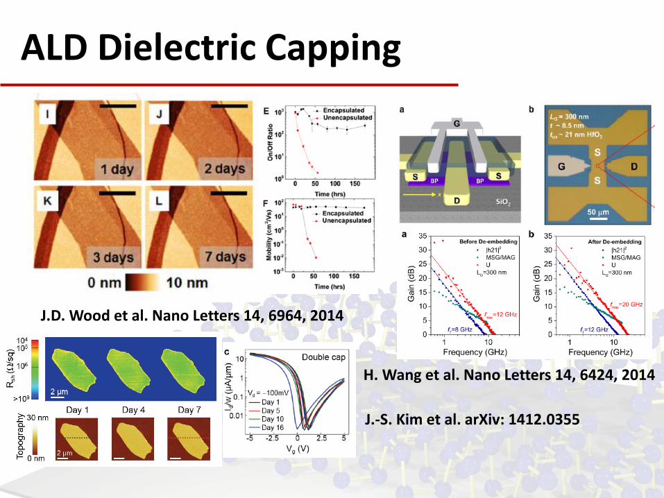
ALD Dielectric Capping
JD Wood et al Nano Letters 14 6964 2014
H Wang et al Nano Letters 14 6424 2014
J-S Kim et al arXiv 14120355
h-BNphosphoreneh-BN Capping
L Li et al arXiv 14116572 N Gillgren et al 2D Materials 2 1001 2015
Similar work also reported V Tayari et al arXiv14120259 X Chen et al arXiv 14121357 A Avsar et al arXiv 14121191 RA Doganov et al arXiv 14121274 Y Cao et al arXiv 150203755
Metal Contacts
Ni-Contact Ambipolar Pd-Contact P-type
-40 -20 0 20 4010
-2
10-1
100
101
102
Vds= 001 V
Vds= 05 V
Dra
in C
urr
en
t (m
Am
m)
Back Gate Voltage (V)
FE
=1705 cm2Vs
Ni
0
5
10
15
20
25
-40 -20 0 20 40
10-2
10-1
100
101
102
Vds= 001 V
Vds= 05 V
Dra
in C
urr
en
t (m
Am
m)
Back Gate Voltage (V)
FE
=1865 cm2Vs
Pd
0
5
10
15
20
25
30
35
Band edge alignment
φbe
φbh
EC
EV EF Rc=15-20 Ωmiddotmm
N-type and P-type Doping Technique on Phosphorene is under development
-40 -20 0 20 40
100
101
102
P-type Pd-contact
BP Transistors
Vds = 05 V
L = 100 nm
L = 200 nm
L = 500 nm
L = 2 m
Dra
in C
urr
ent (m
Am
m)
Back Gate Voltage (V)-40 -20 0 20 40
100
101
102
Ambipolar Ni-contact
BP Transistors
Vds = 05 V
L = 100 nm
L = 200 nm
L = 500 nm
L = 2 m
Dra
in C
urr
en
t (m
Am
m)
Back Gate Voltage (V)
Scaling Properties
Long-channel Short-channel
Enhanced Ambipolarity
Ni-Contact Pd-Contact
Фse
Vds
Фse
Vds Reduced SB width
Y Du et al ACS Nano 2014 10 nm Back-gated Phosphorene FET is under development
2D CMOS Logic
VDD
VOUT
GND
VIN
VDD
GND
VIN VOUT
Phosphorene PMOS
MoS2 NMOS
SiSiO2 substrate
Al2O3 dielectric
TiAu contacts
TiAu metal gates
H Liu et al ACS Nano March 2014
2D CMOS Logic - VTC
-10 -8 -6 -4 -2
00
02
04
06
08
10
Vo
ut (V
)
Vin (V)
VDD=1V
00
03
06
09
12
15
Gain
2D Hetero-structure
Y Deng et al ACS Nano July 2014
BP Homo-junction Y Deng et al IEDM 2014 Also M Buscema et al Nano Letters 2014
Photo-response of BPMoS2 pn diode
Maximum photo-detection responsivity of 418 mAW
PV energy conversion with an external quantum efficiency of 03
Energy harvesting of BPMoS2 pn diode
Other phosphorene work on photonic applications
M Buscema et al Nano Letters 2014
M Engel et al Nano Letters 2014
T Low et al PRB 90 081408 2014
Summary
bull Single-layer phosphorene is demonstrated first time with strong PL peak and Raman shift
bull High performance transistor are achieved on few-layer phosphorene crystals An on-current of 194 mAmm and field-effect hole mobility of 286 cm2Vs are obtained
bull Anisotropic transport is observed at the orthogonal direction and attributed to different effective mass
bull Dielectric capping temporalthermal stability metal contacts and scaling properties are investigated with phosphorene transistors
bull 2D CMOS inverter and 2D p-n diode are demonstrated with n-type MoS2 p-type phosphorene
Acknowledgement
Prof Jun Lou Prof Pulickel Ajayan Mr Sina Najmaei
Prof David Tomanek Mr Zhen Zhu
Han Liu (Intel) Adam Neal (AFRL) Yuchen Du Yexin Deng Lingming Yang Zhe Luo Prof X Xu
Prof James CM Hwang Mr Xi Luo Yaghoob Rahbarihagh
Acquiring Black P from vendors
$100 in ebay by the end of 2012 $800 similar quantity
a factor of 8 increases
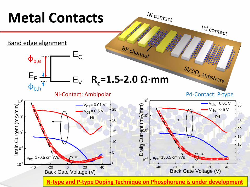
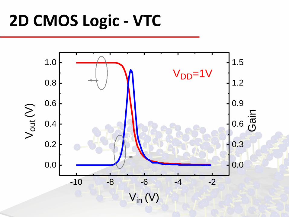
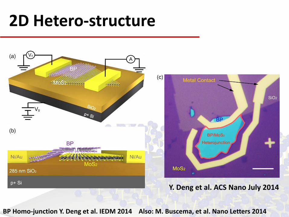
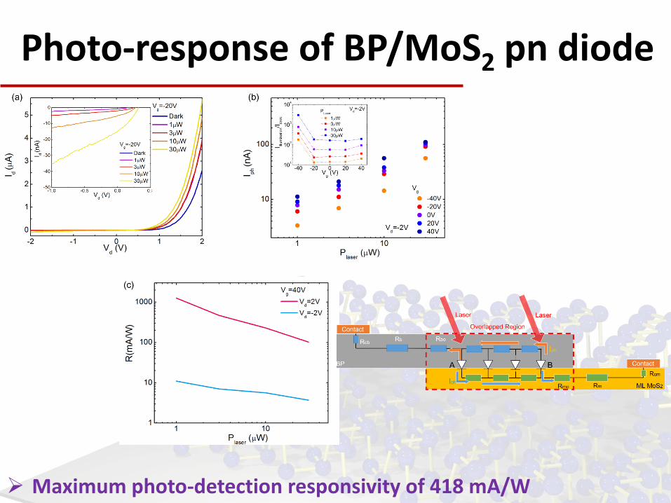
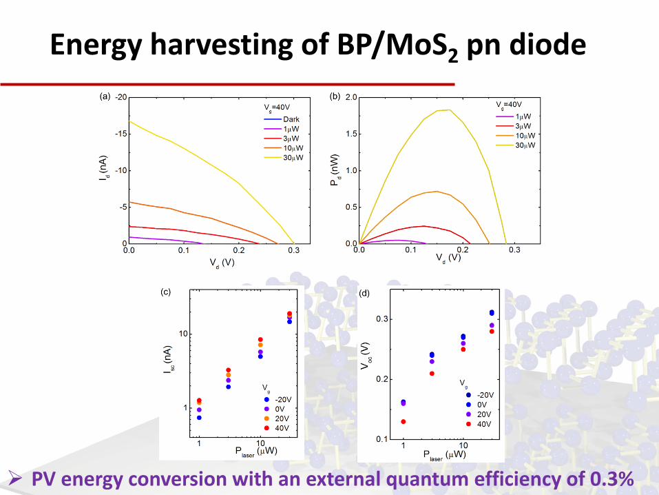

Acquiring Black P from vendors
$100 in ebay by the end of 2012 $800 similar quantity
a factor of 8 increases


![HPLC Determination of Four Textile Dyes and …...dye, [Wavelength 510 nm, 607 nm, 484 nm and 411 nm, mobile phase 0.45 M CTAB in acetonitrile: water (60: 40, v/v)]. 41 Figure 3.4.b](https://static.fdocuments.in/doc/165x107/5f259de32846a26eaa25efe1/hplc-determination-of-four-textile-dyes-and-dye-wavelength-510-nm-607-nm.jpg)
![Telescope Alignment and Wavefront Sensing · ZERNIKES [ nm] CALIBRATION px contours in nm 9.907 m 9.922 m. CHARA Collaboration Year-Seven Science Review E2 9/17/2010 nm nm P V 606](https://static.fdocuments.in/doc/165x107/5fd08587754bdd64ab4edd52/telescope-alignment-and-wavefront-zernikes-nm-calibration-px-contours-in-nm-9907.jpg)