Best Practices for Successful Rigid-Flex Design ...
32
Best Practices for Successful Rigid-Flex Design Fabrication – Part II Christian Keller Senior Field Application Engineer Altium Europe GmbH Andreas Schilpp Technical Marketing Würth Elektronik CBT
Transcript of Best Practices for Successful Rigid-Flex Design ...

Best Practices for
Successful Rigid-Flex
Design Fabrication – Part II
Christian Keller
Senior Field Application EngineerAltium Europe GmbH
Andreas Schilpp
Technical MarketingWürth Elektronik CBT
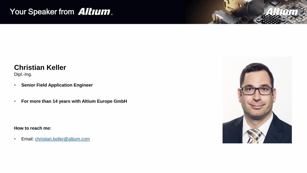
Christian Keller Dipl.-Ing.
• Senior Field Application Engineer
• For more than 14 years with Altium Europe GmbH
How to reach me:
• Email: [email protected]
Your Speaker from

Andreas Schilpp Dipl.-Ing.(FH) Physikalische Technik
• Technical Marketing
• Standards, templates for EDA-tools
• Technical documentation
• Technical trainings live and online
• For more than 25 years with Würth Elektronik CBT
How to reach me:
• Phone: +49 7940 946-330
• Email: [email protected]
Save my contact
details directly in your
address book!
Your Speaker from

Design Flow
1
Final Layout Preparation and Design Rules
Introduction
Material and Stackup
2
3
4
Agenda
Documentation and Demo5
6 Summary, Q&A

Introduction
Objectives
● Present the design process flow for flex-rigid technology
● Learning the new way of finding a suitable stackup
● Present specific flex-rigid design rules
● Demonstrate a flex-rigid PCB design process in AD20

Miniaturisa-tion
Signal Integrity
ReliabilityDynamical Bending
SystemBenefits
Introduction
System advantages of flex-rigid
WE CBT
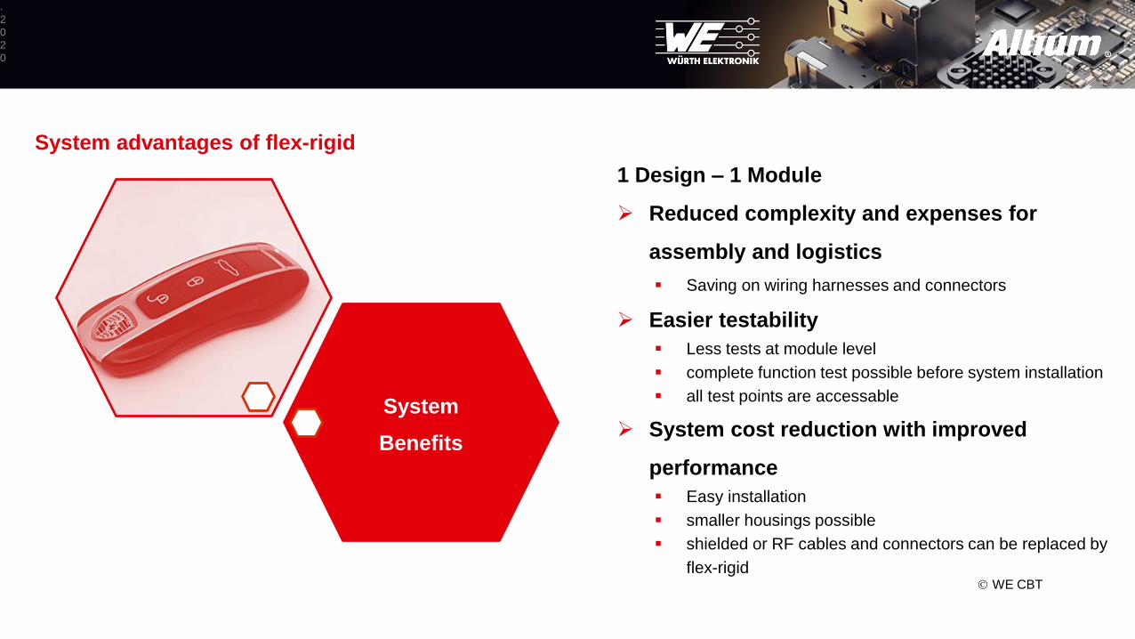
1 Design – 1 Module
Reduced complexity and expenses for
assembly and logistics
Saving on wiring harnesses and connectors
Easier testability
Less tests at module level
complete function test possible before system installation
all test points are accessable
System cost reduction with improved
performance
Easy installation
smaller housings possible
shielded or RF cables and connectors can be replaced by
flex-rigid
6
.
2
0
2
0
System
Benefits
System advantages of flex-rigid
WE CBT

Design Flow
1
Final Layout Preparation and Design Rules
Introduction
Material and Stackup
2
3
4
Agenda
Documentation and Demo5
6 Summary, Q&A

Design Flow
Physical
Design
EDA
LayoutDocumentationMCAD
Material and Stackup
• Materal selection
• Operating conditions
• Functional surface
• Components, esp. critical ones
• Thickness
• Bending radius ratio
• Number of copper layers
• Flex areas (signals, planes)
• Rigid areas
• Via technology (PTH, µVia, BV…)
• Impedance matching
Fabrication Data
• Materal and stackup
• Operating conditions
• Functional surface
• Delivery array
• Gerbers
• AD20 Draftsman
Layout
• Outline, DXF input
• Board planning mode
• Layer stack manager
• Via types
• No vias in flex areas
• Impedance profiles
• Prelim. component placement
• Only on rigid parts
• Routing
• traces, planes
• Design rules
Mechanical Design
• Checking of all interfaces
• Mechanical
• Electrical
• Modular system
• Homogeneous
• Heterogeneous
• Shape and mechanical layout
• Installation concept, foldings
• Bend radii
• IPC use A / use B
• Fastening points
• DXF output

Mechanical Design
Systematic view
• Flex-rigid is mechatronic = mechanic + electronic !
• Multi module systems
• Heterogeneous
• Homogeneous
• Mixed
• Huge impact of mechanical design on
• PCB size
• PCB shape

Where to Start
● Start with the mechanical requirements, specifications, and MCAD outline
● Know why you want to use flex, and visualize how the various rigid and flex regions will be partitioned
● ALWAYS check the circumscribing box
● More examples in Webinar Part I
Mechanical Dimensions and PCB Outline
WE CBT
Where to Start
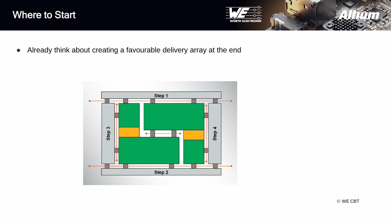
● Already think about creating a favourable delivery array at the end
WE CBT

Bend Radius
● Regard IPC-2223 for design recommendations
● The minimum bend radius will determine the
maximum finished thickness of the flex area
● Length of flex depends on configuration:
Design Flow
1
Final Layout Preparation and Design Rules
Introduction
Material and Stackup
2
3
4
Agenda
Documentation and Demo5
6 Summary, Q&A

The old Way – dangerous!
● Copy and paste of specifications, materials and stackups from old projects
● Finish the complete layout process
● Try to find a PCB manufacturer who makes the boards, at least in prototype volume
● And what about the series? Yield? Reliability? Cost?

Cooperate With Your PCB Manufacturer
● First specify your load profile and material requirements
● Check whether you could use standard stackups wherever possible
● Then talk to your PCB manufacturer and start a project if needed
Download the
import files
right here or
by QR code:

AD20 Material Library
The material library is the basis
● For choosing available materials only
● For choosing the fitting material rigid / flexible
Coverlays
Soldermasks
Cu Foils
Cores
Prepregs
Library
Material
AD20
WE CBT

Stiffeners
● Stiffeners are not needed with flex-rigid
● You can always use a rigid section where you want to place components
● For ZIF contacts you can use a thinned rigid section
WE CBT
Design Flow
1
Final Layout Preparation and Design Rules
Introduction
Material and Stackup
2
3
4
Agenda
Documentation and Demo5
6 Summary, Q&A
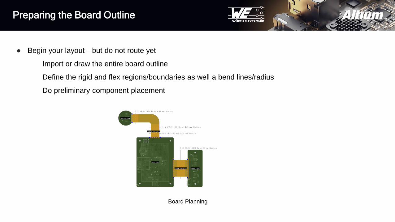
Preparing the Board Outline
● Begin your layout—but do not route yet
Import or draw the entire board outline
Define the rigid and flex regions/boundaries as well a bend lines/radius
Do preliminary component placement
Board Planning

Routing Traces
● Traces on different flex layers should be staggered, not one on top of each other:
● Flex region traces should be curved, not angled, to increase peel strength
● Special rules in the bending area

Planes
● To increase flexibility, planes should be cross-hatched polygon
● For controlled impedance and other applications, however, the cross-hatch may be less than optimal
You may have to pick the lesser of two evils
In some applications, a wide solid strip under critical traces is acceptable
Hatched Polygon (GND)IPC 2223

Via Types
● No vias in flexible areas
● Use teardrops
● Preserve Non Functional Pads = Not used pads on flexible layers for better reliability
WE CBT

• Basic design rules = rigid PCBs
on top:
• Variant specific design rules flex-rigid
• Optional HDI design rules
• Optional Printed Polymer Technologie DR
• Optional Heatsink Technologie DR
• Optional Embedding Technologie DR
• Optional RF DR
• Optional …
Design Rules
WE CBT

Clearance for THT Via pads
Design rules
General parameter definition
Clearance measurement:
related to pad outline!
NOT center of drilling or
via barrel!
Design Rules
WE CBT

Clearance for SMD and THT Via pads
Design rules
Altium parameter setting „G“:
• PCB Rules
• Board Outline Clearance
• Split Barrier
• SMD Pad and TH Pad
Design Rules
WE CBT

Design Flow
1
Final Layout Preparation and Design Rules
Introduction
Material and Stackup
2
3
4
Agenda
Documentation and Demo5
6 Summary, Q&A

Your Fab Drawing
All Drawings
● Board outline with dimensions
● Drill map and drill legend for quality checks
● Any other critical information that is not standard
● All board component data, or indication for
manufacturer to use their standard
Flex specific Drawings
● Application type: Static or Dynamic
● Material and layer stackup
● Dimensions and locations of all rigid and flex regions
● Locations where flex will bend and to what degree
Mechanical Dimensions and Drill Drawing Flex-specific regions, Stackup, and final assembly model
29
Live WebinarDEMO

Design Flow
1
Final Layout Preparation and Design Rules
Introduction
Material and Stackup
2
3
4
Agenda
Documentation and Demo5
6 Summary, Q&A

Thank You for attending