Flex-Rigid Design Guide - we-online.com · Flex-rigid Design Guide V1.0 Flex-rigid circuit boards...
8
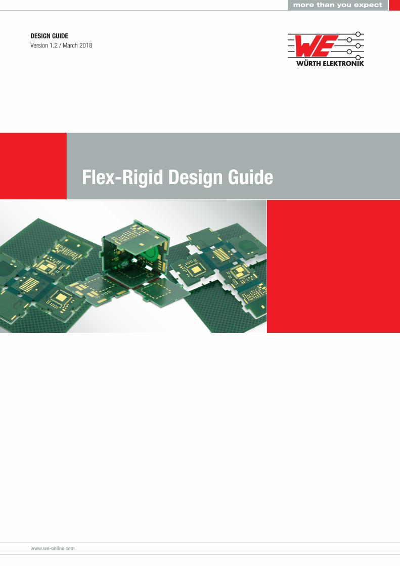
Flex-Rigid Design Guide DESIGN GUIDE Version 1.2 / March 2018 www.we-online.com
-
Upload
nguyennhan -
Category
Documents
-
view
225 -
download
1
Transcript of Flex-Rigid Design Guide - we-online.com · Flex-rigid Design Guide V1.0 Flex-rigid circuit boards...
Flex-Rigid Design Guide
DESIGN GUIDEVersion 1.2 / March 2018
www.we-online.com

www.we-online.com
The trend to miniaturization in electronics continues. Integrated circuit board solutions are becoming more and more popular as a means of effi-ciently utilizing the even smaller casing volume in all three dimensions.
Flexible foils of polyimide with a typical thickness of 50 µm are materials that withstand high temperatures and can be used with copper-cladding as base material for pure flex circuit boards or in combination with rigid base materials for flex-rigid circuit boards with all the prevalent solde-ring methods. Thin FR4 layers in FR4 Semiflex circuit boards are also bendable.
In recent years, Würth Elektronik has accumulated extensive expertise in costumer projects and commissions of the widest variety of designs and applications, from Aerospace to Medical devices and currently it supplies more than 600 customers. With the broad range of technology we offer, you can make the best possible selection for any requirements in terms of performance and costs.
In the following, you will find information about systems that explain the different variants of flex-rigid circuit boards as well as practical tips on design:
1. Systematic view of flex-rigid circuit boards2. Project checklist for system requirements3. Selection of the right technology4. Materials and design parameters5. Mechanical design6. Layout and routing7. Documents for manufacturing flex rigid circuit boards
Basically, standards must be regarded such as IPC-2223, IPC-6013, the Basic Design Guide from Würth Elektronik, as well as variant-specific design rules and our drying recommendations.
Heterogeneous system
Rigid circuit board + wiring harness/ flex soldered in or plugged (detachable)
�� Only few connections�� Non-critical applications�� Wiring errors possible�� Many single parts�� High expenses for test and assembly
Homogeneous system
Circuit boards with identical stack-up in all rigid areas
�� Integrated flex layer(s) throughout�� Considerably greater wiring density�� Saves valuable space by eliminating
connecting points (solder pads or footprint of connectors)
Partially homogeneous system
Sub-systems vary considerably in terms of technology and size: e.g. flex-rigid/connector combination
�� Separable�� Modular systems possible
1. Systematic view of flex-rigid circuit boardsThere are basically different ways to create a system:
PCB1
PCB1
PCB1
PCB2
PCB2
PCB2
PCB1
PCB1
PCB2
PCB2
PCB1 PCB2
PCB1
4-layers
PCB2
HDI 10-layers
02
TIPS: � Integrated wiring should be provided
for the smaller and simpler PCB1.� For pitch ≤ 0.5 mm or shielding
a Board-to-Board connector is recommended.

Flex-rigid circuit boards are mechatronic components. In additi-on to their electronic function, very careful consideration must also be given to mechanical factors:
�� Component assembly, soldering and testing in flat condition in the delivery panel�� Separating, configuring and installing
Advantages:�� Significantly less space required due to three-dimensional wiring �� Elimination of additional components such as connectors and
connecting cables�� Improved signal transmission through elimination of cross-sectional
changes to conductors (connectors, cable, solder connections)�� Weight reduction�� More valuable component assembly and wiring space�� Reduced logistical complexity�� Solution of difficult contacts is possible, simplification of assembly�� Considerably improved reliability of the entire system (a homo-
geneous unit is considerably more reliable than one with connectors and cable)�� Combination with HDI Microvia technologies (microvia, buried via,
finest conductor width) is possible�� Combination with heatsink technology is possible�� Remarkable improvement of testability. Complete system could be
tested prior to system assembly. All components and test points are still accessable.
The design phase decides the later cost structure, so all electrical and mechanical interfaces must be taken into consideration during the con-ceptual phase.
An exact selection of the best components and substrate technology is also necessary in order to be able to fulfill reliably the required operating conditions. Product development also includes getting a precise picture of component assembly, the soldering process, the test and the device assembly.
Cooperation of all participants of the value-added chain
Comp. AComp. A Comp. BComp. B Comp. C
Comp. EComp. E Comp. DComp. D Comp. C
product development
PCB production
assembly and test
03
2D
3D
„The benefits come from the system not through purchasing!“
Andreas SchilppFlex/flex-rigid projects: Interdisciplinary cooperation in development is indispensable!
www.we-online.com
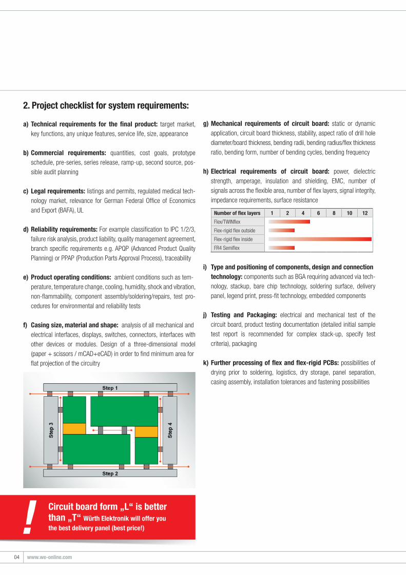
2. Project checklist for system requirements:
a) Technical requirements for the final product: target market, key functions, any unique features, service life, size, appearance
b) Commercial requirements: quantities, cost goals, prototype schedule, pre-series, series release, ramp-up, second source, pos-sible audit planning
c) Legal requirements: listings and permits, regulated medical tech- nology market, relevance for German Federal Office of Economics and Export (BAFA), UL
d) Reliability requirements: For example classification to IPC 1/2/3, failure risk analysis, product liability, quality management agreement, branch specific requirements e.g. APQP (Advanced Product Quality Planning) or PPAP (Production Parts Approval Process), traceability
e) Product operating conditions: ambient conditions such as tem- perature, temperature change, cooling, humidity, shock and vibration, non-flammability, component assembly/soldering/repairs, test pro- cedures for environmental and reliability tests
f) Casing size, material and shape: analysis of all mechanical and electrical interfaces, displays, switches, connectors, interfaces with other devices or modules. Design of a three-dimensional model (paper + scissors / mCAD+eCAD) in order to find minimum area for flat projection of the circuitry
g) Mechanical requirements of circuit board: static or dynamic application, circuit board thickness, stability, aspect ratio of drill hole diameter/board thickness, bending radii, bending radius/flex thickness ratio, bending form, number of bending cycles, bending frequency
h) Electrical requirements of circuit board: power, dielectric strength, amperage, insulation and shielding, EMC, number of signals across the flexible area, number of flex layers, signal integrity, impedance requirements, surface resistance
i) Type and positioning of components, design and connection technology: components such as BGA requiring advanced via tech- nology, stackup, bare chip technology, soldering surface, delivery panel, legend print, press-fit technology, embedded components
j) Testing and Packaging: electrical and mechanical test of the circuit board, product testing documentation (detailed initial sample test report is recommended for complex stack-up, specify test criteria), packaging
k) Further processing of flex and flex-rigid PCBs: possibilities of drying prior to soldering, logistics, dry storage, panel separation, casing assembly, installation tolerances and fastening possibilities
flex cores not glued
Circuit board form „L“ is better than „T“ Würth Elektronik will offer you the best delivery panel (best price!)
04
Number of flex layers 1 2 4 6 8 10 12
Flex/TWINflex
Flex-rigid flex outside
Flex-rigid flex inside
FR4 Semiflex

Flex / TWINflex®
2F (Flex)
2F-Ri (TWINflex)
4F with microvias 1-2/2-3/3-4
�� Very thin flexible foil PI /LCP�� 1 to 6 copper layers�� Partially reinforced with stiffener�� Photosensitive solder mask foil or
Polyimide coverlay�� Delivered individually or as panel
NOTE: Flex-rigid 1F-0Ri design can be more affordable than a TWINflex 1F-Ri
In comparison:
1F-Ri (TWINflex)
1F-0Ri (flex-rigid)
3. Selection of the right technologyPossible variants:
Flex-rigid
1F-3Ri
2F-2Ri
3Ri-2F-3Ri
3Ri-8F-3Ri
�� Components on stable rigid section�� Flexible area 1 to 12 layers bonded/
unbonded (airgap) �� Flexible Polyimide layers out-side
or symmetrically inside �� Rigid areas: standard soldermask�� Flexible area: highly flexible
soldermask or Polyimide coverlay
FR4 Semiflex
Semiflex 1Ri-3Ri
Semiflex 2Ri-4Ri
�� Rigid FR4 circuit boards with deep milling process �� Affordable�� Clearly defined installation situation
and large bending radius�� Bending area: 1 or 2 copper layers,
flex soldermask or Polyimide coverlay
NOTE: �� Often more affordable than a
connector-cable-connector solution�� Definitely better and cheaper
compared to shielded connector and cables�� Usage of bending tools recommended
05
FR4 core
stiffener

www.we-online.com
Indicators for preferential use of individual variants:
4. Materials and design parameters - standardsIPC class 2, use A (flex-to-install)
Variant Indicators for Comments
Flex xF
Very small, dense circuits Microvias and contour possible with laser
Very limited installation space Flexible foil 50 µm thick
Use in vacuum Practically no gas emission
Use at high temperatures PI can be used up to 200°C (without solder mask)
High frequency applications Good thickness tolerance, copper treatment flat, small loss factor
Vias in flexible area But NOT permitted in bending area!
TWINflex xF-Ri Cooling problem Metal reinforcement (heatsink)
FR4 Semiflex
Flex-to-install with large bending radii Affordable solution, miniaturization
Large board with angled connector Only bendability is necessary
Flex material not permitted Only rigid base materials
Flex-rigid 1F-xRi
Large portion of flex surface Laser-cut panel very stable
1:1 wiring across flexible area More affordable than xRi-2F-xRi
Small bending radii Thin flexible area, highly flexible soldermask or cover foil
Short drying times Flex layer on outside
Flex-rigid 2F-xRi High-frequency component-to-connector connection across flexible area with reference layer
No vias necessary for transfersWARNING: complex (see table below)
Flex-rigid xRi-1F-xRiHighly-dynamic prolonged bending Copper in neutral phase ideal
High-level reliability requirements -
Flex-rigid xRi-2F-xRiReference layer in flex area due to signal integrity Polyimide with 75 or 100 µm for impedance control
High-level reliability requirements Rugged technology, mechanical stability
Variant Indicators against Comments
Flex xF Wired components or connectors Low mechanical stability
TWINflex xF-Ri Many individual reinforcements Better to use flex-rigid 1F-xRi
FR4 SemiflexS-shaped bending in one surface Do not subject glass mat to tension
Multi-section casing Assembly tolerances have effect on Semiflex area
Flex-rigid 1F-xRi - -
Flex-rigid 2F-xRiLarge circuit boards Design tends to bow and twist
Large quantities limited area, tends to be expensive
Flex-rigid xRi-2F-xRi - -
Indicators against the use of individual variants:
Flexible material Polyimide core 50 µm, up to 70 µm copper, epoxy glue or adhesiveles, coverlay 25 µm partially or flexible solder mask
Rigid material TG 150 FR4 filled, halogen-free: IPC-4101C /128 (92,94,127)
Copper thicknesses Inner layers 18(standard)/35/70 µm base copper, outer layers 12(standard)/18/35 µm + plating ( with 1F-xRi flex layer is outside)
Circuit board thickness Depends on number of layers: flex > 100 µm, flex-rigid/FR4 Semiflex ≥ 0.8 mm
Solder surface ENIG
06
The requirements in the checklist should be analyzed in detail in a discussion of the project with our specialists.
Please look at the Basic Design Guide of Würth Elektronik for design rules regarding structures, via sizes and soldermask.
Enhanced specifications, e.g. regarding material, stack up, application case Use B, on request!
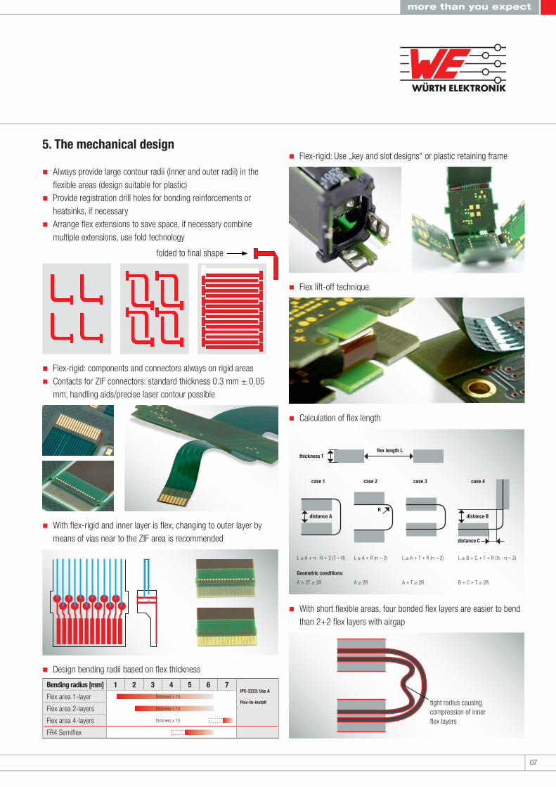
5. The mechanical design
�� Always provide large contour radii (inner and outer radii) in the flexible areas (design suitable for plastic)�� Provide registration drill holes for bonding reinforcements or
heatsinks, if necessary�� Arrange flex extensions to save space, if necessary combine
multiple extensions, use fold technology
�� Flex-rigid: components and connectors always on rigid areas�� Contacts for ZIF connectors: standard thickness 0.3 mm ± 0.05
mm, handling aids/precise laser contour possible
�� With flex-rigid and inner layer is flex, changing to outer layer by means of vias near to the ZIF area is recommended
�� Design bending radii based on flex thickness
�� Flex-rigid: Use „key and slot designs“ or plastic retaining frame
�� Flex lift-off technique
�� Calculation of flex length
�� With short flexible areas, four bonded flex layers are easier to bend than 2+2 flex layers with airgap
folded to final shape
tight radius causing compression of inner flex layers
07
L ≥ A + π · R + 2 (T – R)
A + 2T ≥ 2R A ≥ 2R A + T ≥ 2R B + C + T ≥ 2R
Geometric conditions:
L ≥ A + R (π – 2) L ≥ A + T + R (π – 2) L ≥ B + C + T + R (½ · π – 2)
distance A distance B
distance C
flex length Lthickness T
R
case 1 case 2 case 3 case 4
Bending radius [mm] 1 2 3 4 5 6 7IPC-2223: Use A
Flex-to-installFlex area 1-layer
Flex area 2-layers
Flex area 4-layers
FR4 Semiflex
thickness x 10
thickness x 10
thickness x 10
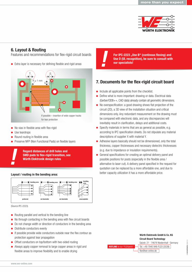
Layout / routing in the bending area:
(Source IPC-2223)
�� Routing parallel and vertical to the bending line�� No through contacting in the bending area with flex circuit boards�� Do not change width or direction of conductors in the bending area�� Distribute conductors evenly�� If possible provide wide conductors outside near the flex contour as
protection against tear propagation�� Offset conductors on top/bottom with two-sided routing�� Always apply copper removal to large copper areas in rigid and
flexible areas to improve flexibility and to enable drying
www.we-online.com
bending area
preferred unacceptablenot desirable not desirable
bending area bending area bending area
Regard distances of drill holes and SMD pads to flex-rigid transition, see Würth Elektronik design rules
6. Layout & Routing Features and recommendations for flex-rigid circuit boards
�� Extra layer is necessary for defining flexible and rigid areas
�� No vias in flexible area with flex-rigid�� Use teardrops�� Round routing in flexible area�� Preserve NFP (Non Functional Pads) on flexible layers
If possible – insertion of wide copper tracks
for tear protection
C G
GR ≥ 1 mm
Würth Elektronik GmbH & Co. KG
Circuit Board Technology
Salzstr. 21 · 74676 Niedernhall · Germany
Tel: +49 7940 946-FLEX (3539)
HOTLINE to our “FLEXperts”
For IPC-2223 „Use B“ (continous flexing) and Use D (UL recognition), be sure to consult with our specialists!
7. Documents for the flex-rigid circuit board
�� Include all applicable points from the checklist.�� Define what is more important: drawing or data. Electrical data
(Gerber/ODB++, CAD data) already contain all geometric dimensions.�� No overspecification: a good drawing shows flat projection of the
circuit (2D), a 3D view of the installation situation and critical dimensions only. Any redundant measurement on the drawing must be compared with electronic data, and any discrepancies will inevitably result in clarification, delays and additional costs.�� Specify materials in terms that are as general as possible, e.g.
according to IPC specification sheets. Do not stipulate any material descriptions of supplier X with material Y.�� Adhesive layers basically should not be dimensioned, only the total
thickness, copper thicknesses and necessary dielectric thicknesses (e.g. due to impedance or insulation requirements).�� General specifications for creating an optimal delivery panel and
possible positions for posts (especially in the flexible area /alternative to laser cut). A delivery panel specified in the request for quotation can be replaced by a more affordable one, and due to better capacity utilization it has a more affordable price.
DIENECKARPRINZEN_0318_FLY