BENQ LCD Q7C4 (FP71V+) Spare Parts List · bitmap OSD, and keypad controlling. The output data are...
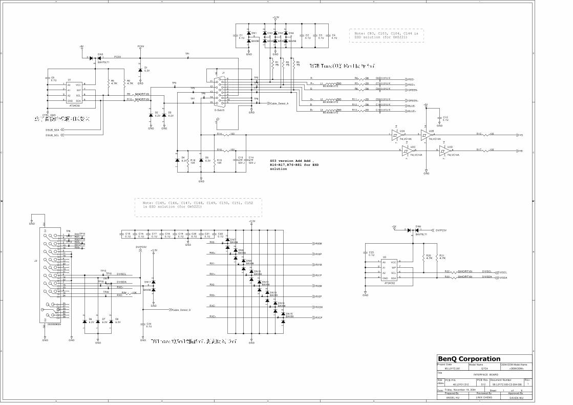
58
BENQ LCD Q7C4 (FP71V+) Spare Parts List P/N: 99.L0Y72.ESE/ESA/EST ITEM DESCRIPTION PART NO. LOCATION 1 PCBA I/F BD Q7C4 GLARE MI 55.L0Y01.013 2 IC OVERDRIVE VTI03601 LQFP208 71.03601.00E U11 3 IC LCD CTRL GM5221(BQ6100) 208P 71.05221.B0E U4 4 IC EEPROM AT24C02N-10SI-1.8SON 72.02402.C01 U1,U3 5 IC EEPROM AT24C16AN-10SI-1.8SON 72.02416.N01 U7 6 IC FLASH PM39LV020-70JC PLCC32 72.39020.C33 U5 7 IC SDRAM K4S161622H-TC60 TSOP 72.61622.209 U13,U14,U15,U16 8 IC CMOS 74LVC14A SO-N 14P 73.07414.061 U2 9 IC RESET V6300C LO-2.8V SOT23 74.06300.C3B U6 10 IC VR G952T-63U 4P SOT223 74.95263.03C U8 11 IC DR G960T63U SOT-223 3P 74.96063.03C U10 12 PCBA SPS BD NEW INVERTER GLARE 55.L0Y02.003 13 PCBA CTRL BD ACCACM MI 55.L0Y03.011 14 LCDM 17 M170EG01 V.3/AUO 56.91L83.061 15 ASSY RC ABS Y5003A Q7C4 60.L0Y04.001 16 ASSY COLUMN ABS Y5003A Q7C4 60.L0Y05.001 17 ASSY BZL ABS 8020C Q7C4-FP71V+ 60.L0Y16.002 18 CTN B 456*423*157 Q7C4/BENQ 44.L0Y01.002 19 CSN F EPS Q7C4 47.L0Y01.001 20 CSN B EPS Q7C4 47.L0Y02.001 21 SIGNAL/C DVI-D 20276 2000MM BK 50.L3012.501 22 CABLE SIGNAL 15/15P CORE*1 1.5M 50.L9005.501 23 CD MANUAL FP71V+ Q7C4 53.L0Y03.001 24 ASSY PACK BASE Q7C4 60.L0Y07.003 * THIS PARTS LIST MAY BE SUBJECT TO CHANGE WITH PRIOR NOTICE BY CSD OF BENQ. Page : 1 / 1
Transcript of BENQ LCD Q7C4 (FP71V+) Spare Parts List · bitmap OSD, and keypad controlling. The output data are...

BENQ LCD Q7C4 (FP71V+) Spare Parts ListP/N: 99.L0Y72.ESE/ESA/EST
ITEM DESCRIPTION PART NO. LOCATION
1 PCBA I/F BD Q7C4 GLARE MI 55.L0Y01.013
2 IC OVERDRIVE VTI03601 LQFP208 71.03601.00E U11
3 IC LCD CTRL GM5221(BQ6100) 208P 71.05221.B0E U4
4 IC EEPROM AT24C02N-10SI-1.8SON 72.02402.C01 U1,U3
5 IC EEPROM AT24C16AN-10SI-1.8SON 72.02416.N01 U7
6 IC FLASH PM39LV020-70JC PLCC32 72.39020.C33 U5
7 IC SDRAM K4S161622H-TC60 TSOP 72.61622.209 U13,U14,U15,U16
8 IC CMOS 74LVC14A SO-N 14P 73.07414.061 U2
9 IC RESET V6300C LO-2.8V SOT23 74.06300.C3B U6
10 IC VR G952T-63U 4P SOT223 74.95263.03C U8
11 IC DR G960T63U SOT-223 3P 74.96063.03C U10
12 PCBA SPS BD NEW INVERTER GLARE 55.L0Y02.003
13 PCBA CTRL BD ACCACM MI 55.L0Y03.011
14 LCDM 17 M170EG01 V.3/AUO 56.91L83.061
15 ASSY RC ABS Y5003A Q7C4 60.L0Y04.001
16 ASSY COLUMN ABS Y5003A Q7C4 60.L0Y05.001
17 ASSY BZL ABS 8020C Q7C4-FP71V+ 60.L0Y16.002
18 CTN B 456*423*157 Q7C4/BENQ 44.L0Y01.002
19 CSN F EPS Q7C4 47.L0Y01.001
20 CSN B EPS Q7C4 47.L0Y02.001
21 SIGNAL/C DVI-D 20276 2000MM BK 50.L3012.501
22 CABLE SIGNAL 15/15P CORE*1 1.5M 50.L9005.501
23 CD MANUAL FP71V+ Q7C4 53.L0Y03.001
24 ASSY PACK BASE Q7C4 60.L0Y07.003
* THIS PARTS LIST MAY BE SUBJECT TO CHANGEWITH PRIOR NOTICE BY CSD OF BENQ.
Page : 1 / 1


FP71V+(Q7C4) LCD Monitor Service Guide Circuit Operation Theory
1 Confidential
I. Introduction: The Q7C4 is a 17” SXGA (1280x1024), 16.2M colors (R/G/B 6-bit + FRC) TFT LCD monitor with multi-media
function. It’s a Dual (analog and digital) interface LCD monitor with a 15 pins D-sub signal cable and a 24 pins DVI-D cable. It’s compliant with VESA specification to offer a smart power management and power saving function. It also offers OSD menu for users to control the adjustable items and get some information about this monitor, and the best function is to offer users an easy method to set all adjustable items well just by pressing one key, we called it “I-Key” which can auto adjusting all controlled items. Q7C4 also offer DDC2 function to meet VESA standard.
II. Block diagram
The Q7C4 consists of a head and a stand (base). The head consists of a LCD module with 4 lamps, a power board (include AC/DC, DC/DC and inverter board), a control board and an interface board. The block diagram is shown as below.
III. Circuit operation theory:
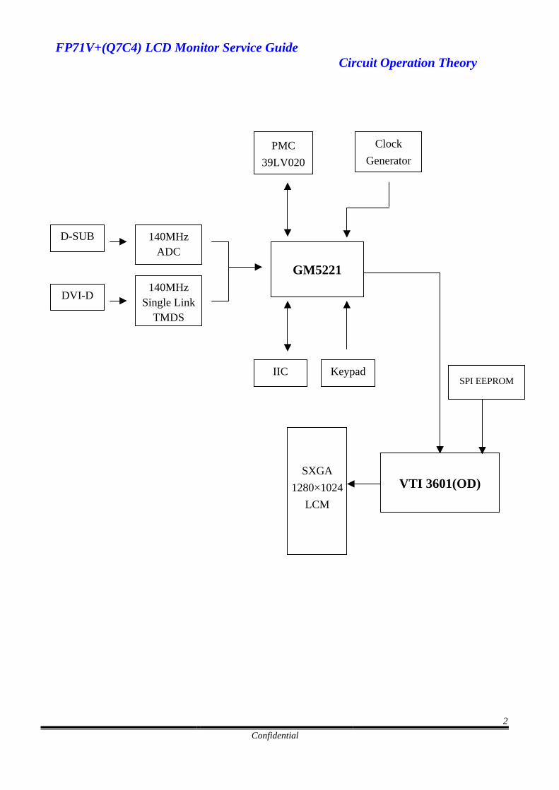
A-1.) Interface board diagram:
Control board
Interface board with OverDrive IC
LCD module with 4 lamps (backlight)
AC power in D-Sub DVI-D
Inverter
& Power
FP71V+(Q7C4) LCD Monitor Service Guide Circuit Operation Theory
2 Confidential
VTI 3601(OD)
SPI EEPROM
GM5221 140MHz
Single Link TMDS
PMC 39LV020
Clock Generator
SXGA 1280×1024
LCM
DVI-D
D-SUB
KeypadIIC
140MHz ADC
FP71V+(Q7C4) LCD Monitor Service Guide Circuit Operation Theory
3 Confidential
(a) Circuit operation theory: A basic operation theory for the interface board is to convert input signal into digital RGB. Analog RGB signal is converted to digital signal through ADC. DVI-D signal is converted through TMDS receiver. The microprocessor GM5221 receives video data and optimizes the image automatically. It also supports input source selection, 16 color from a 64k palette bitmap OSD, and keypad controlling. The output data are sent to LCD module. (b) IC introduction:
1) DDC (Display Data Channel) function: We use DDC IC to support DDC2B function. DDC data is stored in 24C02(EEPROM). Those data related to LCD monitor specification. PC can read them by “SDA” and “SCL” serial communication for I²C communication for DDC2B.
2) GM5221 IC: There are A/D, Scaling and OSD functions in the GM5221 IC. Scaling IC is revolutionary scaling engine, capable of expanding any source resolution to a highly uniform and sharp image, combined with the critically proven integrated 8 bit triple-ADC and patented Rapid-lock digital clock recovery system. It also support detect mode and DPMS control.
3) EEPROM: We use 24C16 to store all the adjustable data and user settings, and use two 24C02s to store DVI and D-Sub EDID data.
4) PMC 39LV020: FrashROM. It contains final firmware. 5) VTI3601 IC: OverDrive IC. It can decrease the LCD response time. 6) ATMEL 25F512N: Serial EEPROM. It store OD table.
FP71V+(Q7C4) LCD Monitor Service Guide Circuit Operation Theory
4 Confidential
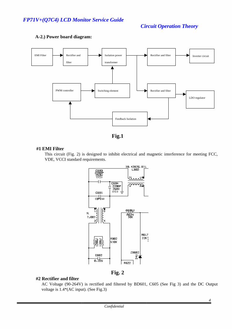
A-2.) Power board diagram:
Fig.1
#1 EMI Filter
This circuit (Fig. 2) is designed to inhibit electrical and magnetic interference for meeting FCC, VDE, VCCI standard requirements.
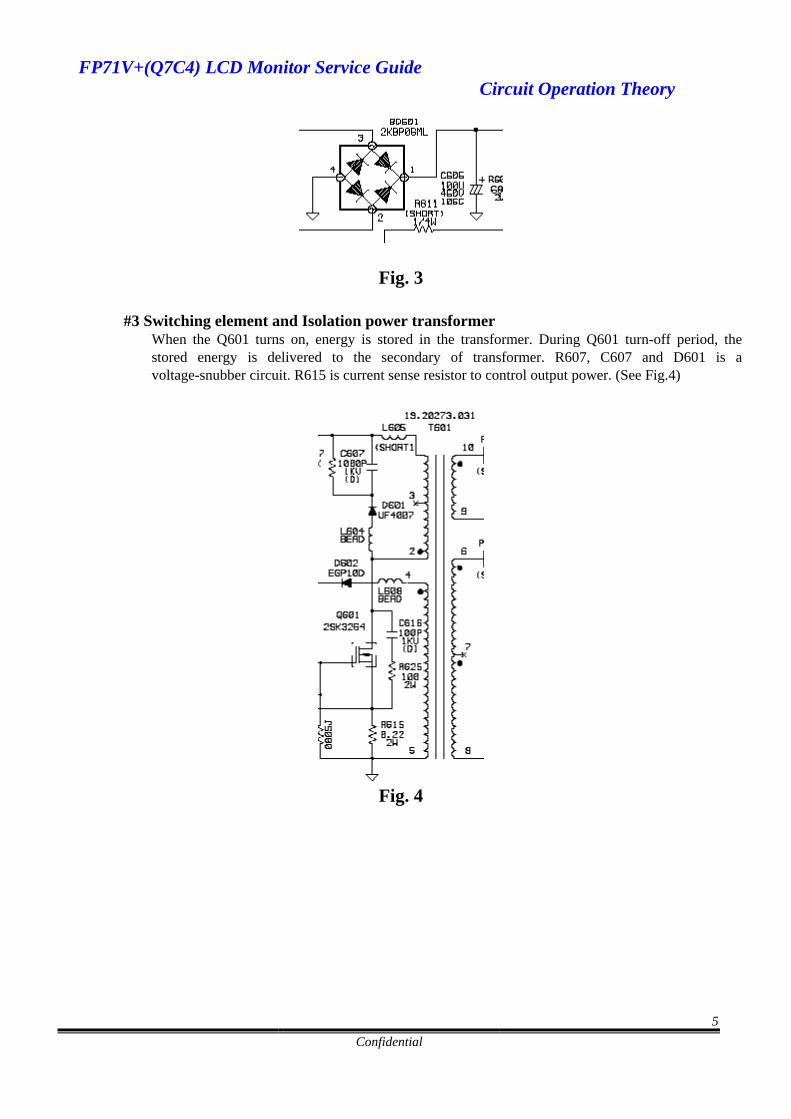
Fig. 2 #2 Rectifier and filter
AC Voltage (90-264V) is rectified and filtered by BD601, C605 (See Fig 3) and the DC Output voltage is 1.4*(AC input). (See Fig.3)
EMI Filter Rectifier and
filter
Isolation power
transformer
Rectifier and filter
PWM controller Switching element
Feedback Isolation
Rectifier and filter
LDO regulator
Inverter circuit
FP71V+(Q7C4) LCD Monitor Service Guide Circuit Operation Theory
5 Confidential
Fig. 3
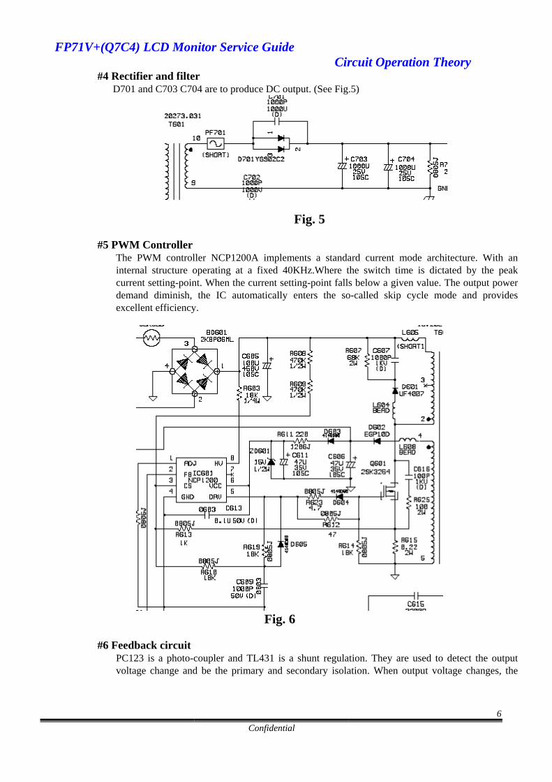
#3 Switching element and Isolation power transformer When the Q601 turns on, energy is stored in the transformer. During Q601 turn-off period, the stored energy is delivered to the secondary of transformer. R607, C607 and D601 is a voltage-snubber circuit. R615 is current sense resistor to control output power. (See Fig.4)
Fig. 4
FP71V+(Q7C4) LCD Monitor Service Guide Circuit Operation Theory
6 Confidential
#4 Rectifier and filter D701 and C703 C704 are to produce DC output. (See Fig.5)
Fig. 5
#5 PWM Controller The PWM controller NCP1200A implements a standard current mode architecture. With an internal structure operating at a fixed 40KHz.Where the switch time is dictated by the peak current setting-point. When the current setting-point falls below a given value. The output power demand diminish, the IC automatically enters the so-called skip cycle mode and provides excellent efficiency.
Fig. 6
#6 Feedback circuit
PC123 is a photo-coupler and TL431 is a shunt regulation. They are used to detect the output voltage change and be the primary and secondary isolation. When output voltage changes, the

FP71V+(Q7C4) LCD Monitor Service Guide Circuit Operation Theory
7 Confidential
feedback voltage will be compared and duty cycle will be decided to control the correct output voltage. (See Fig.7)
Fig.7
A-3.) Inverter diagram:
1.Block Diagram
2. General Specification Input Voltage: 14.5V Input Current: 2A max. ON/OFF Voltage: 3.3V
Output Requirement: Max. Output Current: 8mA Min. Output Current: 3mA Lamp Working Voltage: 700Vrms Open Lamp Voltage: 1500Vrms Frequency: 40-80KHz
3.Circuit Operation Theorem
15Vin ON/OFF
switching
OSCILATOR
CIRCUIT
TRANSFORMER CCFL
PWM CONTROLLER
TL1451 CIRCUIT PROTECTION
AND DETECT
ON/OFF
BRT_ADJ

FP71V+(Q7C4) LCD Monitor Service Guide Circuit Operation Theory
8 Confidential
3.1 ON/OFF SWITCH
The turn-on voltage was controlled by R815 and R816.The inverter was turned on or off by the switching transistors Q801 and Q802, Also regulator IC801 is control by Q801 and Q802 decide supply 12.5V to inverter part or instead.

FP71V+(Q7C4) LCD Monitor Service Guide Circuit Operation Theory
9 Confidential
3.2 PWM Control circuit
TL1451 is a dual PWM controller. C807 and R811 decide the working frequency. BLT_ADJ signal is from control board, control pulse width then decide how much energy delivery to CCFL also decide CCFL brightness. Q803 and Q804 be the buffer to rise the drive capability and the totem poles circuit can improve a capable of driving for Q805.C813 decide the striking time delay.

FP71V+(Q7C4) LCD Monitor Service Guide Circuit Operation Theory
10 Confidential
3.3 Oscillator Circuit
Royer circuit uses the characteristic of transformer saturation to oscillate. When the DC power inject, Q808 or Q809 will turns on, and the current Ic increases. After a period, the transistor will leave the saturation status and Vce increase. The result causes the voltage of primary coil get lower. Finally the transistor turn off, and another transistor turn on. These statuses are repeated and the pin7 and pin8 of T801 will get a Sin Wave to turn on CCFL.
A-3.) Audio block diagram:
DC POWERINPUT
POWER ICTDA7496
AUDIOINPUTConnect with
8 ohm/2W Speaker
Connect withPC Audio output
The audio block consists of an audio board and dual speaker drivers. The speaker drivers are using 62 x 33 x 20 mm2 audio box (rated 2W/CH) with DC volume control, power is supplied by power board and audio input is from PC audio output (Line Out). 1. Power IC: Use ST POWER IC TDA7496 which is stereo AB Class output amplifiers with
DC volume control. The devices are designed for use in TV and monitor, but are also suitable for battery-feed portable recorders and radios. Use +14.5V from power board and connect speaker drivers to offer 1W/CH.
2. DC Power Input: To supply +14.5V for TDA7496 power source. 3. Audio Input: Connect with PC audio output in 3.5mm to 3.5mm signal line.
FP71V+(Q7C4) LCD Monitor Service Guide Circuit Operation Theory
11 Confidential
4. Speaker driver: Use 8 ohm / 62 x 33 x 20 mm2 speaker driver (rated 2W/CH). 5. DC Volume Control: The voltage range is 0 ~ 3.3V (from MCU).
A-4.) Control board introduction:
The main parts of the control board are a push button, and a LED. (a) Push button: It’s a simple switch function. Pressing it for “ON” to do the auto adjustment,
select (unselect) adjustment or adjusting bar. (b) LED: It indicates the DPMS status of this LCD monitor; blue light means DPMS on
(Normal operating condition), amber light means DPMS off (Power off condition).
FP71V+ (Q7C4) LCD Monitor Service Guide Trouble Shooting
1 Confidential
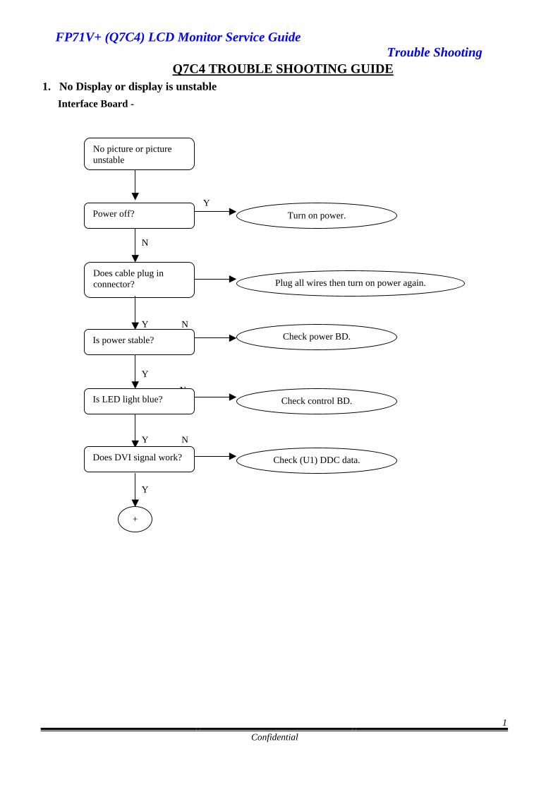
Q7C4 TROUBLE SHOOTING GUIDE 1. No Display or display is unstable
Interface Board -
Y
N
N
Y N
Y
N
Y N
Y
No picture or picture unstable
Power off? Turn on power.
Does cable plug in connector? Plug all wires then turn on power again.
Is power stable? Check power BD.
Is LED light blue? Check control BD.
Does DVI signal work? Check (U1) DDC data.
+

FP71V+ (Q7C4) LCD Monitor Service Guide Trouble Shooting
2 Confidential
N
Y N
Y N
Y
N
Y
Check Panel or replace it.
Is LED status normal? Check MCU (U4) or replace it.
+
Check crystal (Y2) CKT or replace it. Does crystal work correctly?
Is LED status normal? Replace interface BD or check scaler Mst 7131B
Does LVDS cable connect to panel?
Plug LVDS cable again or replace it.

FP71V+ (Q7C4) LCD Monitor Service Guide Trouble Shooting
3 Confidential
2. BUTTON function Control board -
N
Y N
Y
N
Y
OSD doesn’t work.
Is control BD working? Plug control BD then retry.
Check Interface BD.
Is button switch working? Replace control BD then
Check Interface BD L7~L12, R55~R60, R41, R42, RN1, RN2 OK?
Replace component then

FP71V+ (Q7C4) LCD Monitor Service Guide Trouble Shooting
4 Confidential
3. OSD function
N
Y
4. OD function
Picture Abnormal
OSD display OK? Change another I/F BD
Change I/F BD and contact RD
N
Y
OSD doesn’t work
Is control BD working? Replace control BD
Check Interface BD

FP71V+ (Q7C4) LCD Monitor Service Guide Trouble Shooting
5 Confidential
4. Power Board
Backlight didn't shine
LED shined?
3.3V existed? IS I/F board connected?
IC801 PIN 9 IS12~16V?
Check IC801
PWM existed?(BLT_ADJ)
Plug CN701 again orchecking I/F BD
Turn on level existed?(BLT_ON)
Insert them againCheck CN801~CN804was pluged properly?
Plug CN601 again orchecking PW BD
ReplaceIC801,Q805,Q812
Replace new fuse
Replace new fuse
Check IC701 OK?
Checking F601Broke?
Check IC601 Vccexisted?
Replace IC602,IC702,D701 or check
I/F BD
Replace IC701
Replace new fuse
Replace IC601,Q602,
Y
N
N
N
N
Y
Y
Y
Y
N
Y
Y N
N
Y
Y
Y
N
N
N
FP71V+(Q7C4) LCD Monitor Service Guide Alignment Procedure
1
Confidential
Table of Contents
1. ALIGNMENT PROCEDURE (FOR FUNCTION ADJUSTMENT)...........................................................................................................2 The list of necessary alignment for a LCD monitor ...................................................................................................................2 A. Preparation............................................................................................................................................................................2 B. Geometry adjustment & checking (for preset timing modes).................................................................................................2 C. ADC calibration (White Balance)..........................................................................................................................................2 D. Color temperature adjustment...............................................................................................................................................3 E. Writing EDID data into monitor............................................................................................................................................3 F. Command definition...............................................................................................................................................................3
2. EEPROM MAPPING...................................................................................................................................................................6 3. AUDIO TEST PROCEDURE ..........................................................................................................................................................7
A. Audio spec..............................................................................................................................................................................7 B. Audio Test Procedures...........................................................................................................................................................7
4. WIRE DRESSING ........................................................................................................................................................................8 - ASSEMBLY STEP BY STEP.............................................................................................................................................................8 6. ADD GLUE...............................................................................................................................................................................17

FP71V+(Q7C4) LCD Monitor Service Guide Alignment Procedure
2
Confidential
1. Alignment procedure (for function adjustment) The list of necessary alignment for a LCD monitor
Items Description Remark 1 Geometry adjustment & checking For Preset timing modes 2 ADC calibration (Auto color balance adjustment) UVGA7 (1024x768/75Hz) 3 Color temperature adjustment C1/Bluish, C2/Reddish & C3/sRGB 4 Writing EDID data into monitor Analog/DVI-D
A. Preparation 1. Setup input timing to any preset modes or patterns. 2. Enter factory mode (press “EXIT” & “ENTER” & “Power” buttons at the same time to turn on monitor). 3. Press “I-Key” into “Burn In Mode” tag and select “On” to enable burn-in mode. 4. Power off the monitor, remove the input source and then power on again. 5. Setup unit and keep it warm up for at least 30 minutes.
B. Geometry adjustment & checking (for preset timing modes)
1. Enter factory mode (press “EXIT” & “ENTER” & “Power” buttons at the same time to turn on monitor). 2. Select timing mode from figure-1 and input full screen display pattern to monitor. 3. Select “Auto Adjust” to run “AUTO” function for geometry adjustment. 4. Check if the position, phase and clock of the image are correct to make sure controlled functions and performance are
ok. 5. Select “Recall All ” to erase user settings. 6. Turn off the monitor power. 7. Turn on the monitor power again to check if monitor’s image settings are ok and with following settings.
CONTRAST = 50 BRIGHTNESS = 90 COLOR = Reddish (default setting) OSD time = 20 VOLUME = 30
Figure-1: Preset Timing modes list Input Timing Actual Output
Resolution Horizontal Frequency (KHz)
Vertical Frequency (Hz)
Dot Clock Frequency (MHz)
Actual display Resolution
OK N.A Remark
720x400 31.47(N) 70.08(P) 28.32 1280x1024 √ DOS 800x600 46.87(P) 75.00(P) 49.5 1280x1024 √ VESA
1024x768 48.36(N) 60.00(N) 65.00 1280x1024 √ VESA 1024x768 60.02(P) 75.00(P) 78.75 1280x1024 √ VESA 1152x870 68.68(N) 75.06(N) 100.00 1280x1024 √ Mac
1152x900 71.81(N) 76.14(N) 108.00 1280x1024 √ VESA 1280x1024 80.00(P) 75.00(P) 135.00 1280x1024 √ VESA 1280x1024 81.18(N) 76.16(N) 135.09 1280x1024 √ SUN
C. ADC calibration (White Balance)
~~Analog only, it is not required for DVI-D input source

FP71V+(Q7C4) LCD Monitor Service Guide Alignment Procedure
3
Confidential
1. Setup input timing UVGA7 (1024x768/75Hz), pattern 42 (5-Mosaic pattern with white color block) with Analog signals from Chroma video pattern generator. (it depends on Scaler IC supplier’s recommendation)
2. Enter factory mode (press “EXIT” & “ENTER” & “Power” buttons at the same time to turn on monitor). 3. Press “I-Key” into “Burn In Mode” tag and select “On” to enable burn-in mode. 4. Change color temperature from “Reddish” (default) to “User Preset”. 5. Press hot-key “CONTRAST” to run “White Balance” function. (This procedure will get optimal gain/offset (clamp)
values) 6. Checking if the picture is ok, or reject this monitor and check its circuit board or wire/cable connection.
D. Color temperature adjustment 1. Setup input timing to any preset modes, pattern 41 (full white color pattern) with Analog signals from Chroma video
pattern generator. 2. Enter factory mode (press “EXIT” & “ENTER” & “Power” buttons at the same time to turn on monitor). 3. Make sure ADC calibration (White Balance) had already been done. 4. Measure color temperature by Minolta CA-110 (or equivalent equipment). 5. Adjust the color temperature ~~ Two methods can be used to adjust RED, GREEN, BLUE value of each color
temperature, C1/Bluish, C2/Reddish & C3/sRGB to meet following spec. requirement, the 1st method is by using external PC and IIC alignment protocol to do automatic adjustment, and the 2nd method is by manually and must be in factory mode.
Color temperature X+- 0.283+(-) 0.03 (C1/9300K/Bluish set on OSD) Y+- 0.297+(-) 0.03 Color temperature X+- 0.326+(-) 0.03 (C2/5800K/Reddish set on OSD) Y+- 0.342+(-) 0.03 Color temperature X+- 0.313+(-) 0.03 (C3/6500K/sRGB set on OSD) Y+- 0.329+(-) 0.03
6. Turns off the monitor power.
E. Writing EDID data into monitor 1. Setup a PC with DDC card. 2. Connect PC to monitor with a D-sub signal cable. 3. Please refer to the C212 for the correct EDID file. 4. Runs the writing program to write the analog EDID data into EEPROM for analog input (ie. 15-pin D-sub). 5. Repeat step 4 and write the digital EDID data into EEPROM for DVI-D input (ie. 24-pin DVI-D). 6. Read both EEPROM data and confirm it to match with the C212 definition. (Note: The DVI-D input may not operation correctly if the digital EDID data do not exist.)
F. Command definition
PC Host will send 0x7C IIC slave address and then following 4 bytes command
I2C Send Command Byte1 Byte2 Byte3 Byte4 OK N.A. Remark
Write Contrast to MCU RAM CA 55 Data cksum √
Write Brightness to MCU RAM CA 56 Data cksum √
Write Red Gain to MCU RAM CA 57 Data cksum √
Write Green Gain to MCU RAM CA 58 Data cksum √
Write Blue Gain to MCU RAM CA 59 Data cksum √
Write data to MCU RAM and update the related register to refresh the screen immediately.Don’t store data to EEPROM.
Read Contrast from MCU RAM C3 55 XX cksum √
Read Brightness from MCU RAM C3 56 XX cksum √

FP71V+(Q7C4) LCD Monitor Service Guide Alignment Procedure
4
Confidential
Read Red Gain from MCU RAM by color index C3 57 XX cksum √
Read Green Gain from MCU RAM by color index C3 58 XX cksum √
Read Blue Gain from MCU RAM by color index C3 59 XX cksum √
Base on current color index to read back the right gain value.
Write C1 (Bluish) R-Gain Data to EEPROM AA 3C Data cksum √
Write C1 (Bluish) G-Gain Data to EEPROM AA 3D Data cksum √
Write C1 (Bluish) B-Gain Data to EEPROM AA 3E Data cksum √
Write C2 (sRGB) R-Gain Data to EEPROM AA 4C Data cksum √
Write C2 (sRGB) G-Gain Data to EEPROM AA 4D Data cksum √
Write C2 (sRGB) B-Gain Data to EEPROM AA 4E Data cksum √
Write C3 (Reddish) R-Gain Data to EEPROM AA 5C Data cksum √
Write C3 (Reddish) G-Gain Data to EEPROM AA 5D Data cksum √
Write C3 (Reddish) B-Gain Data to EEPROM AA 5E Data cksum √
Write User R-Gain Data to EEPROM AA 6C Data cksum √
Write User G-Gain Data to EEPROM AA 6D Data cksum √
Write User B-Gain Data to EEPROM AA 6E Data cksum √
Write Cx R-Gain Data to EEPROM AA 7C Data cksum √
Write Cx G-Gain Data to EEPROM AA 7D Data cksum √
Write Cx B-Gain Data to EEPROM AA 7E Data cksum √
Reserved for some model have extra color temperature
Write Contrast to EEPROM AA 92 Data cksum √
Write Brightness to EEPROM AA 93 Data cksum √
Write C/T index to EEPROM AA 94 0~4 cksum √
1=C1/9300/Bluish, 2=C2/6500/sRGB, 3=C3/5800/Reddish,
4=User, 5=Cx
Write OSD-Hpos to EEPROM AA 95 Data cksum √
Write OSD-Vpos to EEPROM AA 96 Data cksum √
Write Language to EEPROM AA 97 0~7 cksum √
0=DE, 1=EN, 2=ES, 3=FR,
4=IT, 5=JA, 6=繁中, 7=簡中
(Also Update MCU RAM)
Write EEPROM OSD Timer AA 98 Data cksum √
Write EEPROM Volume AA 99 Data cksum √
Write EEPROM Gamma index AA 9A Data cksum √ For model with Gamma curve selection function
Write OSD Transparency to EEPROM AA 9E Data cksum √
Write OSD Rotation to EEPROM AA 9F Data cksum √
Read C1 (Bluish) R-Gain data from EEPROM A3 3C XX cksum √
Read C1 (Bluish) G-Gain data from EEPROM A3 3D XX cksum √
Read C1 (Bluish) B-Gain data from EEPROM A3 3E XX cksum √
Read C2 (sRGB) R-Gain data from EEPROM A3 4C XX cksum √
Read C2 (sRGB) G-Gain data from EEPROM A3 4D XX cksum √
Read C2 (sRGB) B-Gain data from EEPROM A3 4E XX cksum √
Read C3 (Reddish) R-Gain data from EEPROM A3 5C XX cksum √
Read C3 (Reddish) G-Gain data from EEPROM A3 5D XX cksum √
Read C3 (Reddish) B-Gain data from EEPROM A3 5E XX cksum √

FP71V+(Q7C4) LCD Monitor Service Guide Alignment Procedure
5
Confidential
Read User R-Gain data from EEPROM A3 6C XX cksum √
Read User G-Gain data from EEPROM A3 6D XX cksum √
Read User B-Gain data from EEPROM A3 6E XX cksum √
Read Cx R-Gain data from EEPROM A3 7C XX cksum √
Read Cx G-Gain data from EEPROM A3 7D XX cksum √
Read Cx B-Gain data from EEPROM A3 7E XX cksum √
Reserved for some model have extra color temperature
Read Contrast from EEPROM A3 92 XX cksum √
Read Brightness from EEPROM A3 93 XX cksum √
Read C/T index from EEPROM A3 94 XX cksum √
1=C1/9300/Bluish, 2=C2/6500/sRGB, 3=C3/5800/Reddish, 4=User, 5=Cx
Read OSD-Hpos EEPROM A3 95 XX cksum √
Read OSD-Vpos from EEPROM A3 96 XX cksum √
Read Language from EEPROM A3 97 XX cksum √ 0=DE, 1=EN, 2=ES, 3=FR, 4=IT, 5=JA, 6=繁中, 7=簡中
Read OSD Timer from EEPROM A3 98 XX cksum √
Read Volume from EEPROM A3 99 XX cksum √
Read Gamma index from EEPROM A3 9A XX cksum √ For model with Gamma curve selection function
Read OSD Transparency from EEPROM A3 9E XX cksum √
Read OSD Rotation from EEPROM A3 9F XX cksum √
Change Color Temp. to C1/9300K/Bluish CC 01 XX cksum √
Change Color Temp. to C2/6500K/sRGB CC 02 XX cksum √
Change Color Temp. to C3/5800K/Reddish CC 03 XX cksum √
Change Color Temp. to User CC 04 XX cksum √
Change C/T immediately. And store C/T index to EEPROM.
Change Color Temp. to Cx CC 05 XX cksum √ Reserved
Change Input Source to D-Sub CD 01 XX cksum √
Change Input Source to DVI CD 02 XX cksum √
On burn in mode CE 01 XX cksum √ Store data to EEPROM
Off burn in mode CE XX* XX cksum √ XX* = Non “1” value Store data to EEPROM
Monitor is forced power saving CF 01 XX cksum √
Monitor wake up from power saving CF XX* XX cksum √ XX* = Non “1” value
User mode to factory mode 1A 5A XX cksum √
Auto Color (Offset1, Offset2, Gain) 1B 5A XX cksum √
Copy EDID Serial number to EEPROM 1C 5A XX cksum √ For specified “Industry Customer” model.
Factory mode to User mode 1E 5A XX cksum √
Clear user mode and factory recall 1F 5A XX cksum √ Store data to EEPROM
Write EDID data to MCU DDC RAM 55 NA NA NA √ For MTV312 MCU type
Copy DDC RAM data to EEPROM BB NA NA NA √ For MTV312 MCU type
Drive WP pin to low to enable write DDC IC 55 NA NA NA √ For stand alone DDC IC
Drive WP pin to high to disenable write function BB NA NA NA √ For stand alone DDC IC
EEPROM Bank R/W (For Debug using only, not for Production Line Write EEPROM directly)
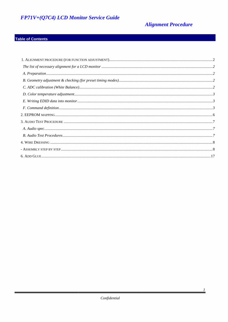
Read EEPROM Bank 0 B0 Address XX cksum √
Read EEPROM Bank 1 B1 Address XX cksum √
FP71V+(Q7C4) LCD Monitor Service Guide Alignment Procedure
6
Confidential
Read EEPROM Bank 2 B2 Address XX cksum √ (For 24C08 type)
Read EEPROM Bank 3 B3 Address XX cksum √ (For 24C08 type)
Write EEPROM Bank 0 B8 Address Data cksum √
Write EEPROM Bank 1 B9 Address Data cksum √
Write EEPROM Bank 2 BA Address Data cksum √ (For 24C08 type)
Write EEPROM Bank 3 BB Address Data cksum √ (For 24C08 type)
Note A: Byte4 (cksum) = Byte1 + Byte2 + Byte3
Note B: Data = The value write to MCU or EEPROM
Note C: XX = don't care, any value (<=0xFF).
When PC Host sends 0x7D command to MCU, MCU must return as following (2 bytes)
Return Code R-Byte1 R-Byte2
Checksum error code FC AA
Normal return code the above Byte3 (/data) FC
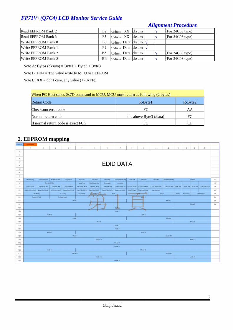
If normal return code is exact FCh FC CF 2. EEPROM mapping

FP71V+(Q7C4) LCD Monitor Service Guide Alignment Procedure
7
Confidential
3. Audio Test Procedure A. Audio spec.
Amplifier Spec. Note Input Sensitivity @ 1KHz 1Vrms Output Power 1Wrms/CH THD @1KHz 1W (%) <1% S/N Ratio (dB) >40dB Cross Talk <-50dB R/L Channel Check OK Pop Sound Check OK Speaker Nominal Speaker Impedance @1KHz 1V 8 Ohm±15% Resonant Frequency 180~20KHz SPL-10dB Rated/Max Power 2W/3W Output SPL @2W 50cm 84 ± 3 dB (1W 0.5M) Distortion <5%
B. Audio Test Procedures
1.) PC Playback (a) Plug in the Audio input to a PC I/O ports. (b) Playback a specified CD, listening to the playback music.
Reject criteria:
(a) Playback sound is not clear or distorted. (b) Loss of high or low frequencies. (c) Abnormal or no sound is heard.
2.) Left and right speaker functions and polarity check
(a) Playback music by switching off the right channel, listen to the music. (b) Playback music by switching off the left channel, listen to the music.
Reject criteria:
(a) Both left and right channels sounded. (b) The left and right channels playback are reversed. (c) Abnormal or no sound is heard during right or left channels playback.
3.) Volume control check (a) Playback and listen to the music. (b) Turn the volume control from normal position to maximum then to minimum then back to normal position again.
Reject criteria:
(a) The sound output level is not decrease or increase smoothly. (b) Abnormal sound is heard during the volume control is turning. (c) Sound is heard when the volume control turn to minimum. (d) No increase or decrease of sound level when turning the volume control.
4.) Power saving

FP71V+(Q7C4) LCD Monitor Service Guide Alignment Procedure
8
Confidential
(a) Playback and listen to the music. (b) Into power saving mode, the Left and Right speakers is muted.
Reject criteria: (a) The Left & Right speakers output are not muted. (b) One of the Left or Right speaker is not muted.
4. Wire Dressing - Assembly step by step
A. Screw up Speaker Drivers on the Bazel. (4 screws)

FP71V+(Q7C4) LCD Monitor Service Guide Alignment Procedure
9
Confidential
B. Put the Clip together with the Ctrl BD.
C. Connect the speaker wires to the Ctrl BD on the both sides.
FP71V+(Q7C4) LCD Monitor Service Guide Alignment Procedure
10
Confidential
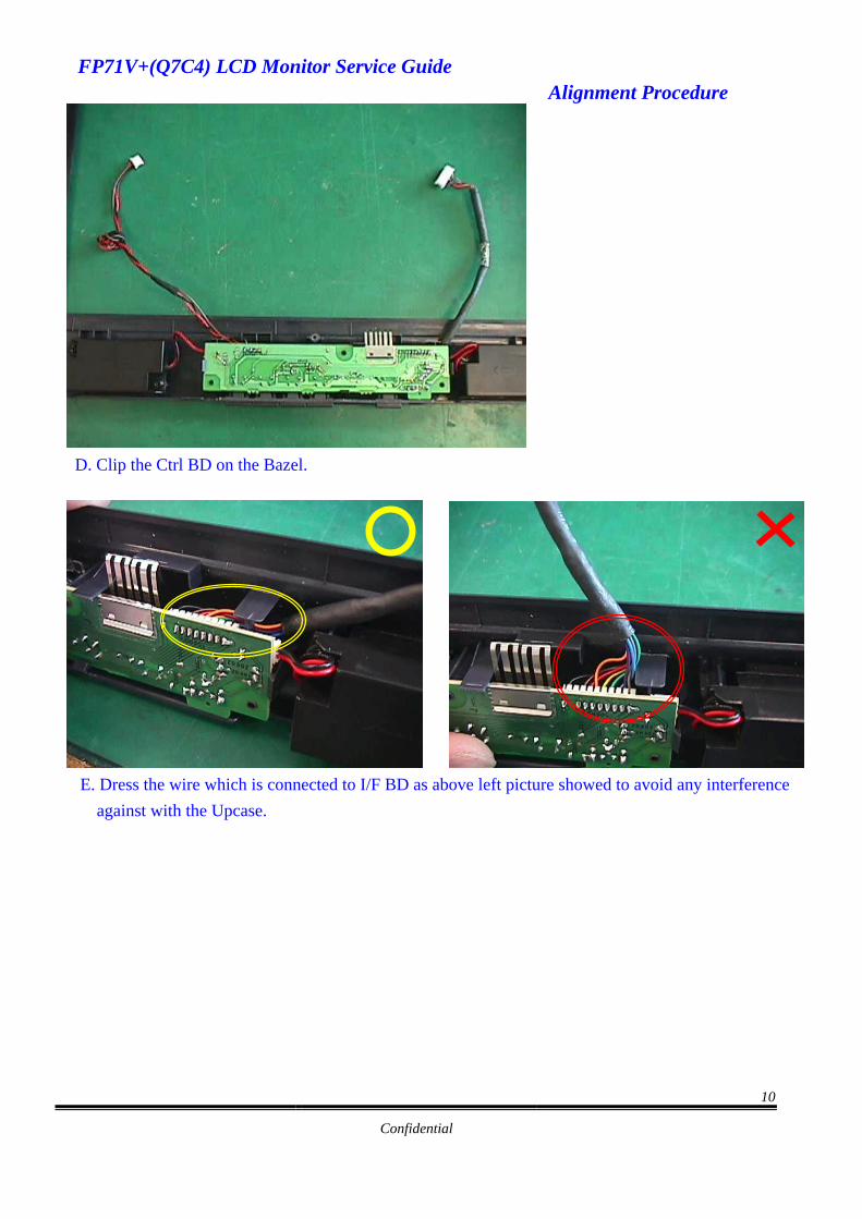
D. Clip the Ctrl BD on the Bazel.
E. Dress the wire which is connected to I/F BD as above left picture showed to avoid any interference
against with the Upcase.

FP71V+(Q7C4) LCD Monitor Service Guide Alignment Procedure
11
Confidential
F. Assembly the panel with the Main Bracket. (4 side-mount)
G. Check the 2 gaskets if stuck on the Main Bracket.

FP71V+(Q7C4) LCD Monitor Service Guide Alignment Procedure
12
Confidential
H. Insert the LVDS FFC into the panel connector and stick the yellow tape on them.
I. Assembly the I/F & Power BD together with the Main Bracket. J. Screw up the boards (6 screws) and connect wires (lamp wires & FFC).
FP71V+(Q7C4) LCD Monitor Service Guide Alignment Procedure
13
Confidential
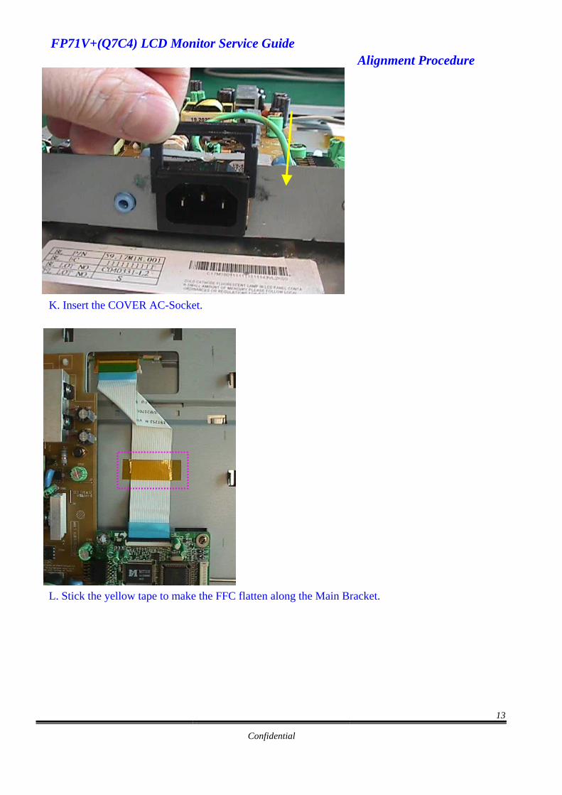
K. Insert the COVER AC-Socket.
L. Stick the yellow tape to make the FFC flatten along the Main Bracket.

FP71V+(Q7C4) LCD Monitor Service Guide Alignment Procedure
14
Confidential
M. Assembly the Main Cover with the Main Bracket. (1 screw)
N. Put the Head set together with the Bazel set.

FP71V+(Q7C4) LCD Monitor Service Guide Alignment Procedure
15
Confidential
O. Make sure if the Clip touch the panel firmly.
P. Connect the wires with the I/F & Power BD.

FP71V+(Q7C4) LCD Monitor Service Guide Alignment Procedure
16
Confidential
Q. The method to clip the Ctrl BD wire.
R. Assembly the Upcase (5 screws) and the Base (2 screws).

FP71V+(Q7C4) LCD Monitor Service Guide Alignment Procedure
17
Confidential
6. Add Glue
C605 (Power BD)
5
5
4
4
3
3
2
2
1
1
D D
C C
B B
A A
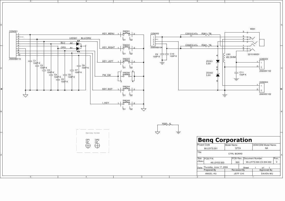
KEY_EXIT
I _KEY
KEY_RIGHTORG
PW_SW
KEY_LEFT
KEY_MENU
BLU
Title
Size Document Number R ev.
Date: Sheet o f
Project Code
Reviewed By Approved ByPrepared By
Model Name
PCB P/N PCB Rev.
��������������OEM/ODM Model Name
99.L0Y72.000-C3-304-002
CTRL BOARD
1 1
JEFF CHI DAVEN WU
48.L0Y03.S03 S03
ANGEL HU
<Size>
Q7C499.L0Y72.001
2
Thursday, June 17, 2004
NA
Spring holes
SW3031 2
G2G1
OPOP1
C7100P K
CON304
2060091102
11
22
C302 0.47u
OPOP2
R301 75
SW3041 2
G2G1
C1100P K
C9100P K
CON301
2060089110
12345678910 L301
45 OHM
R302 75
C3100P K SW306
1 2
3 4C5100P K
LED301 BLU/ORG
A1
A2J
M301
2210165031
33
55
44
66
77
22
11
ZD3025.6V
AK
C10100P K
ZD3015.6V
AK
C8100P K
R303 0
C2100P K
SW3011 2
G2G1
CON302
2060089104
1234
C4100P K
SW3021 2
G2G1
C11100P K
SW3051 2
G2G1
C6100P K
CON303
2060091102
11
22
C301 0.47u

FP71V+(Q7C4) LCD Monitor Service Guide Engineering Specification
1 Confidential
Table of Contents
1. Introduction 3
2. Operational Specification 3 2.1 Power supply ................................................................................................................................ 3 2.2 Signal interface ............................................................................................................................. 4 2.3 Video performance ....................................................................................................................... 5 2.4 Scan range .................................................................................................................................... 5 2.5 Plug & Play DDC2B Support....................................................................................................... 6 2.6 Support Timings ........................................................................................................................... 6
3. Operational & Functional Specification 7 3.1 Video performance ....................................................................................................................... 7 3.2 Brightness Adjustable Range........................................................................................................ 7 3.3 Acoustical Noise ........................................................................................................................... 7 3.4 Environment ................................................................................................................................. 7 3.5 Transportation............................................................................................................................... 8 3.6 Electrostatic Discharge Requirements .......................................................................................... 8 3.7 EMC ............................................................................................................................................. 8 3.8 Reliability ..................................................................................................................................... 9 3.9 Audio performance ....................................................................................................................... 9
4. LCD Characteristics 9 4.1 The Physical definition & Technology summary of LCD panel................................................... 9 4.2 Optical characteristics of LCD panel............................................................................................ 9
5. User Controls 10 5.1 User’s hardware control definition ............................................................................................... 10 5.2 OSD control function definition ................................................................................................... 10
6. Mechanical Characteristics 11 6.1 Dimension..................................................................................................................................... 11 6.2 Weight........................................................................................................................................... 11 6.3 Plastic ........................................................................................................................................... 11 6.4 Carton ........................................................................................................................................... 12
FP71V+(Q7C4) LCD Monitor Service Guide Engineering Specification
2 Confidential
Table of Contents
7. Pallet & Shipment 12 7.1 Container Specification ................................................................................................................ 12 7.2 Carton Specification ..................................................................................................................... 12
Product: ................................................................................................................................ 12 Package:................................................................................................................................ 12
8. Certification 13
Appendix: Physical Dimension Front View and Side view 14

FP71V+(Q7C4) LCD Monitor Service Guide Engineering Specification
3 Confidential
1. Introduction This specification describes Q7C4, which is a 17.0” analog and digital interface color TFT LCD monitor with audio. The monitor supports up to 1280x1024 pixel resolution and refresh rate of 75 Hz. The independent 6 bits R, G, B colors are capable of displaying 16.2M colors (RGB-6bit + FRC data). In addition, dithering function is supported. The features summary is shown below, *All panel spec. in C201 definition depends on the variance of panel source.
Feature items Specifications Remark Panel supplier & module name Yes AUO M170EG01 V.3 Screen diagonal Yes 432(17.0”) Display Format Yes RGB Pixel Pitch Yes 0.264x0.264 Viewing Angle (@ Contrast Ratio = 10) Yes 70/70/70/60 Analog interface with Scaling supported Yes Genesis GM5221 DVI interface with Scaling supported Yes Genesis GM5221 Video interface with Scaling supported No Max resolution mode supported Yes 1280x1024@76Hz Number of Display Colors supported Yes 16.2M Contrast Ratio Yes 500:1 Luminance Yes 400 AC power input Yes 90~264V DC power input (with AC power adapter) No DPMS supported Yes <1W(110V) ,<2W(220V) LED indicator for power status showed Yes OSD for control & information supported Yes Multi-language supported for OSD Yes Buttons control supported Yes Flywheel control supported No Scaling function supported Yes Auto adjustment function supported Yes DDC function supported (EDID ver. 1.3) Yes Audio speakers supported Yes Audio Jack (input connector) supported Yes Earphone Jack (input connector) supported Yes Microphone function supported No Mechanical Tilt base design Yes From -2 to +20 degree VESA wall mounting design Yes Mechanical Rotate design No N.A. Mechanical Lift base design No N.A. Kensington compatible lock design Yes
2. Operational Specification 2.1 Power supply
Item Condition Spec OK N.A Remark Input Voltage range Universal input full range 90~264VAC /47~63Hz √ Input Current range 90 ~ 264VAC < 2.0 Arms √ Power Consumption Normal “On” operation < 40 W √

FP71V+(Q7C4) LCD Monitor Service Guide Engineering Specification
4 Confidential
DPMS DPMS “Off” state < 1 W in power preferred
mode, 115V < 2 W, 230V
√
Inrush Current 110 VAC 220 VAC
< 30 A (peak) < 60 A (peak) √
Earth Leakage Current 264 VAC/50Hz < 3.5 mA √
Hi-Pot 1. 1500VAC, 1 sec 2. Ground test: 30A, 1sec
Without damage < 0.1 ohm √
Power Line Transient IEC1000-4-4 1KV √
IEC1000-4-5 (Surge) Common: 2KV, Differential: 1KV √
CCFL operation range 90 ~ 264VAC 3 mA ~8mA √
CCFL Frequency 90 ~ 264VAC 40KHz ~ 80KHz √
Power cord Color: Black Length: 1500 +/- 50 mm √
2.2 Signal interface
Item Condition Spec OK N.A Remark
15-pin D-Sub Color: Black Length: 1500 +/- 30 mm
√
Signal Cable 24-pin DVI-D Color: Black
Length: 2000 +/- 50 mm √
15-pin D-sub connector See Note-1 √ Pin assignment
24-pin DVI-D connector See Note-2 √ Signal type Separate analog R/G/B √
Level 700 mV (peak to peak) √ Video input Impedance 75 Ohms +/- 1.5 Ohms √
Signal type Separate H/V-sync
Composite H/V-sync (Positive/Negative)
√
Level Logic High: 2.4V ~ 5.5V Logic Low: 0V ~ 0.5V
(TTL level) √
Impedance Minimum 2.2KΩ(pull down) √
Sync input
Sync Pulse Width (SPW) 0.7μs < H-SPW 1H < V-SPW
√
Note-1: The pin assignment of 15-pin D-sub connector is as below,
1 5
6 10
11 15
Pin Signal Assignment Pin Signal Assignment 1 Red video 9 PC5V (+5 volt power) 2 Green video 10 Sync Ground 3 Blue video 11 Ground 4 Ground 12 SDA

FP71V+(Q7C4) LCD Monitor Service Guide Engineering Specification
5 Confidential
5 Cable Detected 13 H-Sync (or H+V) 6 Red Ground 14 V-sync 7 Green Ground 15 SCL 8 Blue Ground
Note-2: The pin assignment of 24-pin DVI-D connector is as below,
Pin Signal Assignment Pin Signal Assignment 1 TMDS RX2- 13 Floating 2 TMDS RX2+ 14 +5V Power 3 TMDS Ground 15 Ground 4 Floating 16 Hot Plug Detect 5 Floating 17 TMDS RX0- 6 DDC Clock 18 TMDS RX0+ 7 DDC Data 19 TMDS Ground 8 Floating 20 Floating 9 TMDS RX1- 21 Floating
10 TMDS RX1+ 22 TMDS Ground 11 TMDS Ground 23 TMDS Clock+ 12 Floating 24 TMDS Clock-
2.3 Video performance
Item Condition Spec OK N.A Remark Max. support Pixel rate 135 MHz √ Max. Resolution 1280 x 1024 √
Rise time + Fall time < 6.25 ns
(50% of minimum pixel clock period)
√
Settling Time after overshoot /undershoot
< 5% final full-scale value √
Overshoot/Undershoot < 12% of step function
voltage level over the full voltage range
√
2.4 Scan range
Item Condition Spec OK N.A Remark Horizontal 30 ~ 83 KHz √ Vertical 56 ~ 76 Hz √

FP71V+(Q7C4) LCD Monitor Service Guide Engineering Specification
6 Confidential
2.5 Plug & Play DDC2B Support Item Condition Spec OK N.A Remark
DDC channel type DDC2B √ EDID Version 1.3 √
2.6 Support Timings
Input Timing Actual Output
Resolution Horizontal Vertical Dot Clock Actual display OK N.A Remark
640x350 31.47(P) 70.08(N) 25.17 1280x943 √
720x400 31.47(N) 70.08(P) 28.32 1280x1024 √
640x480 31.47(N) 60.00(N) 25.18 1280x1024 √
640x480 35.00(N) 67.00(N) 30.24 1280x1024 √
640x480 37.86(N) 72.80(N) 31.5 1280x1024 √
640x480 37.50(N) 75.00(N) 31.5 1280x1024 √
800x600 37.88(P) 60.32(P) 40.00 1280x1024 √
800x600 48.08(P) 72.19(P) 50.00 1280x1024 √
800x600 46.86(P) 75.00(P) 49.50 1280x1024 √
832X624 49.72(N) 74.55(N) 57.29 1280x1024 √
1024x768 48.36(N) 60.00(N) 65.00 1280x1024 √
1024x768 56.48(N) 70.10(N) 75.00 1280x1024 √
1024x768 60.02(P) 75.00(P) 78.75 1280x1024 √
1024X768 60.24(N) 74.93(N) 80.00 1280x1024 √
1152x864 67.50(P) 75.00(P) 108.00 1280x1024 √
1152x870 68.68(N) 75.06(N) 100.00 1280x1024 √
1152x900 61.80(N) 66.00(N) 94.50 1280x1024 √
1152x900 71.81(N) 76.14(N) 108.00 1280x1024 √
1280x1024 64.00(P) 60.00(P) 108.00 1280x1024 √
1280x1024 75.83(N) 71.53(N) 128.00 1280x1024 √
1280x1024 80.00(P) 75.00(P) 135.00 1280x1024 √
1280x1024 81.18(N) 76.16(N) 135.09 1280x1024 √ Note-3: “P”, “N” stands for “Positive”, “Negative” polarity of incoming H-sync/V-sync (input timing).

FP71V+(Q7C4) LCD Monitor Service Guide Engineering Specification
7 Confidential
3. Operational & Functional Specification 3.1 Video performance
Item Condition Spec OK N.A Remark
Resolution Any input resolution modes which are under 1280 x 1024 1280 x 1024 √
Contrast ratio 500:1 (typ.) √ Brightness At R/G/B saturated condition 400 cd/m2 (typ.) @ 7.5mA √ Response time Rising + Falling time 8 ms (typ.) √
At Contrast ratio = 10 R/L: 70/70 degrees (typ.) √ Viewing angle
At Contrast ratio = 10 U/D: 70/60 degrees (typ.) √ CIE coordinate of White (0.31, 0.33) +/- (0.03, 0.03) √
Display colors 16.2M colors (RGB 6-bits + FRC data) √
3.2 Brightness Adjustable Range
Item Condition Spec OK N.A Remark
Brightness adjustable rangeAt default contrast level
(saturate point) & Full-white color pattern
(Max. brightness value – Min. brightness value)
≧ 100 cd/㎡ √
400 ~ 105
3.3 Acoustical Noise
Item Condition Spec OK N.A Remark
Acoustical Noise At 1 meter distance & “Audio” function disabled ≦ 40 dB/A √
3.4 Environment
Item Condition Spec OK N.A Remark Operating 0 ~ +40 ℃ √
Temperature Non-operating -20 ~ +60 ℃ √
Operating 10 ~ 90% √ Humidity
Non-operating 10 ~ 90% √ Operating 0~3048m (10,000ft) √
Altitude Non-operating 0~12,192m (40,000ft) √

FP71V+(Q7C4) LCD Monitor Service Guide Engineering Specification
8 Confidential
3.5 Transportation
Item Condition Spec OK N.A Remark (1) Sine wave 5~200Hz 1.5G, 1 octave/min, 15 min dwell on each resonant frequency, all primary axis, one sweep (30 min minimum) per orientation, total of 90+ min. (2) Random 5 ~100 Hz, 0 dB/Oct. 0.015 g2/Hz 100 ~200 Hz, -6 dB/Oct. 200 Hz, 0.0038 g2/Hz Equivalent to 1.47 Grms, All primary axis, 20 min per- orientation, total is 60 min.
(1) Vibration Package, Non-Operating
(3) Procedure: Confirmed sample with appearance and function ready before testing then compare with after test record as brightness, uniformity and contrast ratio. Perform random vibration after sine-wave vibration test.
√
(2) Unpackaged Vibration Unpackaged, Non-Operating
Test Spectrum: 20 Hz 0.0185(g2/Hz) 200Hz 0.0185(g2/Hz) Duration : 5 Minutes Axis : 3 axis ( Horizontal and Vertical axis ,Z axis)
√
(3) Drop Package, Non-Operating 91 cm Height (MP stage) (1 corner, 3 edges, 6 faces) √
(4) Shock Wooden package,
Non-Operating
Waveform: half sine Faces: 6 sides/ per orientation
3 shocks. Duration: <3ms Velocity accelerate: 75g
√
3.6 Electrostatic Discharge Requirements
Item Condition Spec OK N.A Remark
Electrostatic Discharge IEC801-2 standard Contact: 8KV Air: 15KV √
3.7 EMC Item Condition Spec OK N.A Remark
Electric Band 1 < 10 V/m Band 2 < 1 V/m √
TCO03 Magnetic Band 1 < 200nT
Band 2 < 25nT √
FCC part 15J class B EMI
EN55022 class B
After Mass production under 1dBuv for constant measure. Besides DNSF and VCCI class-2 are optional.
√
FP71V+(Q7C4) LCD Monitor Service Guide Engineering Specification
9 Confidential
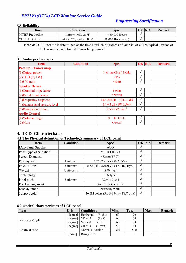
3.8 Reliability Item Condition Spec OK N.A Remark
MTBF Prediction Refer to MIL-217F > 60,000 Hours √ CCFL Life time At 25±2℃, under 7.0mA 50,000 Hours (typ.) √
Note-4: CCFL lifetime is determined as the time at which brightness of lamp is 50%. The typical lifetime of CCFL is on the condition at 7.5mA lamp current.
3.9 Audio performance
Item Condition Spec OK N.A Remark Preamp + Power amp (1)Output power 1 Wrms/CH @ 1KHz √ (2)THD (@ 1W) <1% √ (3)S/N ratio >40dB √ Speaker Driver (1)Nominal impedance 8 ohm √ (2)Rated input power 2 W/CH √ (3)Frequency response 180~20KHz SPL-10dB √ (4)Output sound pressure level 84 ± 3 dB (1W 0.5M) √ (5)Dimension of box 62x33cx20 mm2 √ Audio Control (1)Volume range 0 ~100 levels √ (2)Mute On/Off √
4. LCD Characteristics 4.1 The Physical definition & Technology summary of LCD panel
Item Condition Spec OK N.A Remark LCD Panel Supplier AUO √ Panel type of Supplier M170EG01 V3 √ Screen Diagonal 432mm(17.0”) √ Display area Unit=mm 337.920(H) x 270.336(V) √ Physical Size Unit=mm 358.5(H) x 296.5(V) x 17.0 (D) (typ.) √ Weight Unit=gram 1900 (typ.) √ Technology TN type √ Pixel pitch Unit=mm 0.264 x 0.264 √ Pixel arrangement R/G/B vertical stripe √ Display mode Normally white √ Support color 16.2M colors (RGB 6-bits + FRC data) √
4.2 Optical characteristics of LCD panel
Item Unit Conditions Min. Typ. Max. Remark[degree][degree]
Horizontal (Right) CR = 10 (Left)
60 60
70 70
Viewing Angle [degree][degree]
Vertical (Up) CR = 10 (Down)
60 50
70 60
Contrast ratio Normal Direction 300 500 [msec] Rising Time 6 9

FP71V+(Q7C4) LCD Monitor Service Guide Engineering Specification
10 Confidential
[msec] Rising Time 6 9 [msec] Falling Time 2 4 Response Time [msec] Rising + Falling 8 13
Red x Red y
0.61 0.31
0.64 0.34
0.67 0.37
Green x Green y
0.26 0.58
0.29 0.61
0.32 0.64
Blue x
Color / Chromaticity Coordinates (CIE)
Blue y 0.11 0.04
0.14 0.07
0.17 0.10
White x Color Coordinates (CIE) White White y
0.28 0.30
0.31 0.33
Luminance Uniformity [%] 9 points measurement 75 80 White Luminance @ CCFL 7.5mA (center)
[cd/m2]
TBD 400
Crosstalk (in 75Hz) [%] 1.5
* The test methods for the above items’ definition, please refer to the relative panel specification. 5. User Controls 5.1 User’s hardware control definition
Item Condition Spec OK N.A Remark Monitor Power button √ Enter button √ Right/Inc. button √ Left/Dec. button √ Exit /Volume button √ I-key button √
Mode Selection button √ Mute button √ Input source select button √ 5.2 OSD control function definition
Item Condition Spec OK N.A Remark Auto Adjust Auto-Geometry √ Brightness √ Contrast √ Horizontal Position √ Vertical Position √
Pixel Clock √ Phase √
Color Bluish
Reddish sRGB
User: Separate R/G/B adjustment
√
OSD Position OSD Horizontal position OSD Vertical position √
OSD Time From 5 sec to 60 sec √ Language 8 languages √ Recall Color recall
Recall All √

FP71V+(Q7C4) LCD Monitor Service Guide Engineering Specification
11 Confidential
Mode Selection √ Input Select D-sub
DVI √ Sharpness √ Display Information For input timing √ Volume √
Mute √ Hot key for Brightness √ Hot key for Contrast √ Hot key for Volume √ Hot key for Mode √
* The detailed firmware functions’ specification, please refer to C212 S/W spec. document. 6. Mechanical Characteristics 6.1 Dimension
Item Condition Spec OK N.A Remark Bezel opening 339.8 x 272.2 mm √
Monitor without Stand L x W x H mm 349.7*375.3*72mm √
Monitor with Stand L x W x H mm 385.8*375.3*201.1 mm √
Carton Box (outside) L x W x H mm 456 x 423 x 157mm √
Tilt and Swivel range Tilt: -2 ~ +20 degree
Swivel: 0 degrees √
6.2 Weight
Item Condition Spec OK N.A Remark Monitor (Net) 4.7 Kg √ Monitor with packing (Gross) 6.2 Kg √
6.3 Plastic
Item Condition Spec OK N.A Remark Flammability 94-HB √ Heat deflection To ABS 65 ℃ √ UV stability ABS Delta E < 8.0 √
Resin MPRII: ABS
(VW55/VE0856/D350) √
Texture MT-11020 √ Bezel texture MT-11010
Color BCS-Y5003A √ Bezel painting T8020C

FP71V+(Q7C4) LCD Monitor Service Guide Engineering Specification
12 Confidential
6.4 Carton
Item Condition Spec OK N.A Remark Color Kraft √ Material B Flute √
Compression strength 288 KGF √
Burst Strength 16 KGF/cm2 √
Stacked quantity 13 Layers √
7. Pallet & Shipment 7.1 Container Specification
Stowing Type Container Quantity of products
(sets) (Every container)
Quantity of Products (sets)
(Every Pallet)
Quantity of pallet (sets)
(Every Container)
20' 780 Pallet A: 78 Pallet A: 6
Pallet B: 52 Pallet B: 6
40' 1820 Pallet A: 78 Pallet A: 14
With pallet
Pallet B: 52 Pallet B: 14
20' 974 X X
X X
40' 2099 X X
Without pallet
X X
7.2 Carton Specification Product:
Net Weight (Kg) Gross Weight (Kg) Dimension w/o Base L*W*H (mm)
Dimension w/ Base L*W*H (mm)
4.7Kg 6.2Kg 349.7 x 375.3 x 72 385.82 x 375.3 x 201.1
Package: Carton Interior Dimension (mm)
L*W*H Carton External Dimension (mm)
L*W*H 448 x 415 x 143 456 x 423 x 157

FP71V+(Q7C4) LCD Monitor Service Guide Engineering Specification
13 Confidential
8. Certification
Item Condition Spec OK N.A Remark
Green design API Doc. 715-C49 √
Blue Angel German Standard √
E-2000 Switzerland √
EPA USA Standard √
TCO’99 √
TCO’03 √
Environment
Green Mark √
Microsoft Windows PC98/99 √
DPMS VESA √
DDC 2B Version 1.3 √ PC-Monitor
USB External √
UL (USA) UL60950 3rd edition √
CSA (Canada) CAN/CSA-C22.2 No. 60950 √
Nordic / D.N.S.F EN60950 √
FIMKO EN60950 √
CE Mark 73/23/EEC √ IEC60950 √
EN60950 √
CB EN60950 √
TUV/GS EN60950 /
EK1-ITB 2000:2003 √
CCC (China) √
GOST EN60950 √
Safety
SASO √
CE Mark 89/336/EEC √
FCC (USA) FCC Part 15 B √
EN55022 Class B √
CISPR 22 Class B √
VCCI (Japan) VCCI Class B √
BSMI (Taiwan) CNS 13438 √
EMC
C-Tick (Australia) AS/ NZS CISPR22 √
DHHS (21 CFR) USA X- Ray Standard √ X- Ray Requirement DNHW √

FP71V+(Q7C4) LCD Monitor Service Guide Engineering Specification
14 Confidential
PTB German X- Ray standard √
TUV / Ergo √
ISO 13406-2 √ Ergonomics
prEN50279 √
Appendix: Physical Dimension Front View and Side view
Fig. 1 Physical Dimension Front View and Side view
5
5
4
4
3
3
2
2
1
1
D D
C C
B B
A A
B-
P C5V
RX2-
RX1+
RX0-
RXC+
RXC-
D VISCL
D VISDAD VISCL
RX2+
RX0-
D VISDA
RX1+
RX1-
RX2-
RX2+
RX0+
RX0+
RX1-
RXC+
RXC-
G-
R-
R+
G+
B+
+3.3V
+3.3V
G ND G ND
G ND
G ND
G ND
G ND G ND
G ND
G ND
G ND
G ND
G NDG ND G NDG ND
G ND
+5V P C5V
+3.3V
G ND
+5V
G ND
+5V
CTRL_GND
D SUB_SDA
D SUB_SCL
R ED-
R ED+
GREEN-
BLUE-
BLUE+
GREEN+
DVIPC5V
DVIPC5V
Cable_Detect_A
D VISCL
D VISDA
RX0M
RX0P
RX1M
RX1P
RX2M
RX2P
RXCM
RXCP
HS
VS
Cable_Detect_D
Title
Size Document Number R e v .
Date: Sheet o f
Project Code
R eviewed By Ap proved ByPrepared By
Model Name
P CB P/N PCB Rev.
��������������OEM/ODM Model Name
99.L0Y72.000-C3-304-006
INTERFACE BOARD
1 6
LINIX CHENG DAV EN WU
48.L0Y01.S12 S12
AN GEL HU
<Size>
Q 7C499.L0Y72.001
1
Friday, November 19, 2004
<OEM/ODM>
S03 version Add Add ,R16~R17,R76~R81 for ESDsolution
Note: C83, C103, C104, C144 isESD solution (for Gm5221)
Note: C145, C146, C147, C148, C149, C150, C151, C152is ESD solution (for Gm5221)
� �� ��� �� � � � � �� � � �
��� ��� �� � � � � �� � � ��� � � �� � � �
�� �� �� � ! " #
C 120 .1U
R 214.7K
DN3
BAV99
1
3
2
U2C
74LVC14A
5 6
147
DN 13BAV99
1
3
2
R275
J2
2022009024
1 1
2 2
3 3
4 4
5 5
6 6
7 7
8 8
9 9
10 10
11 11
12 12
13 13
14 14
15 15
16 16
17 17
18 18
19 19
20 20
21 21
22 22
23 23
24 24
C3 27C1 25
C5_ 30C5 29
C4 28C2 26
G1
G1
G2
G2
R 1810K
C9 0.01U K
R 17 100
R7 20
C 200 .1U
TP12
D N6
BAV70LT1
2
3
1
D66.2V
12
R 11 20
L1 Z6068.60060.0T2
D46.2V
12
R 10 SHORT(0)
TP11
L3 Z6068.60060.0T2
D N14BAV99
1
3
2
U 2A
74LVC14A
1 2
147
C 10 0.01U K
R175
C 170 .1U
TP10
R 14 100
TP20
J1
D-Sub15
1728394105
11
12
13
14
15
6
1617
DN1
BAV99
1
3
2
D N4
BAV99
1
3
2
D86.2V
12 DN 15
BAV99
1
3
2
R 13 20
C 180 .1U
TP19
D N7BAV99
1
3
2
U2B
74LVC14A
3 4
147
D16.2V
12
TP5
R 1910K
TP9
R 23 SHORT(0)
D56.2V
12
TP18
C 11 0.01U K
TP3
TP7
C 150 .1U
C7 0.01U K
C 230 .1U
DN8BAV99
1
3
2
U3
AT24C02
A01
A12
A23
GND4
VCC 8
WP 7
SCL 6
SDA 5
TP8
R 12 56
C10 .1U
TP6R9 SHORT(0)
TP1D N5
BAV70LT1
2
3
1
C 160 .1U
TP14
DN9BAV99
1
3
2
C20 .1U
U 2D
74LVC14A
9 8
147
R8 56
TP13
C 1447P50V J
C 210 .1U
R 204.7K
D26.2V
12
R54.7K
D N2
BAV99
1
3
2
D76.2V
12
T1
C30 .1U
C8 0.01U K
R 22 SHORT(0)DN 10BAV99
1
3
2
U1
AT24C02
A01
A12
A23
GND4
VCC 8
WP 7
SCL 6
SDA 5
D N11
BAV99
1
3
2
C 220 .1U
R 15 100
TP4
TP17
C 1347P50V J
R4 56
L2 Z6068.60060.0T2
R 16 100
C40 .1U
R375
D36.2V
12
R 24 10K
DN 12BAV99
1
3
2
TP16
TP2R64.7K
C 240 .1U
C50 .1U
TP15
C 190 .1U
C6 0.01U K

5
5
4
4
3
3
2
2
1
1
D D
C C
B B
A A
RMDATA1RMDATA2RMDATA3
RMDATA6
ROM_CSn
HOST_SDAHOST_SCL
TCLK
R MADDR8
SCLSDA
ROM_OEn
XTAL
RESETn
HOST_SCLHOST_SDA
SCL
SDA
ROM_WEn
ROM_CSn
RMDATA7
RMDATA5RMDATA4RMDATA3RMDATA2RMDATA1RMDATA0
RMDATA6R MADDR14
R MADDR11R MADDR10
R MADDR13
R MADDR15
R MADDR12 R MADDR2
R MADDR0
R MADDR0
R MADDR3
R MADDR1
R MADDR1
R MADDR6
R MADDR3
R MADDR9
R MADDR4
R MADDR10
R MADDR17
R MADDR15
R MADDR4
R MADDR7
R MADDR14
R MADDR16
R MADDR5
R MADDR11
R MADDR7
R MADDR5
R MADDR6
R MADDR9
R MADDR2
R MADDR12R MADDR13
R MADDR8
R MADDR17R MADDR16
R MADDR12
ROM_WEn
RMDATA7
RMDATA5RMDATA4
RMDATA0
TCLKXTAL
RESETn
ROM_OEn
GND
GND
GND
GND
GND
GND
GND
GND
GND
GND
GND
GND
GNDGND
GND
GNDGND
GND
GND
GND GND
GND
GND
3.3V_AVDD
+3.3V
+3.3V
+3.3V
+3.3V
+3.3V
3.3V_LVDS
3.3V_DVDD
+1.8VCVDD_1.8
3.3V_PLL
+1.8V 1.8V_AVDD
+3.3V
+1.8V 1.8V_TMDS
3.3V_AVDD3.3V_PLL
1.8V_PLL
+3.3V
+1.8V
3.3V_LBAD3.3V_PLL
3.3V_AVDD
3.3V_DVDD 1.8V_TMDS
1.8V_AVDD
1.8V_PLL CVDD_1.8 3.3V_LVDS
+3.3V 3.3V_LBAD
GND
GND
GND
+3.3V
+3.3V +3.3V
+3.3V
+3.3V
+3.3V
+3.3V
GND
DSUB_SCLDSUB_SDADVISCLDVISDA
RED+RED-
GREEN+GREEN-
BLUE+BLUE-
HSVS
RX2MRX1PRX1MRX0PRX0M
RXCMRXCP
RX2P
Cable_Detect_A
Cable_Detect_D
BRT_ADJ
Key_Mode
TXE3+TXE3-TXEC+TXEC-TXE2+TXE2-TXE1+TXE1-TXE0+TXE0-
TXO3+TXO3-TXOC+TXOC-TXO2+TXO2-TXO1+TXO1-TXO0+TXO0-
VOLUME_ADJ
LCD_ON_OFFBL_ON
LED_GREENLED_AMBER
PS
VOLUME_SW
AUDIO_MUTE
AUDIO_SRS
KEY_PW _SWKEY_RIGHTKEY_LEFTKEY_MENUKEY_EXITKEY_AUTO
LED_GREEN
LED_AMBER
LCD_ON_OFFBL_ON
Cable_Detect_DCable_Detect_A
Key_Mode
AUDIO_MUTE
AUDIO_SRS
PS
OD_EN
Title
Size Document Number R e v.
Date: Sheet o f
Project Code
Reviewed By Approved ByPrepared By
Model Name
PCB P/N PCB Rev.
��������������OEM/ODM Model Name
99.L0Y72.000-C3-304-006
INTERFACE BOARD
2 6
LINIX CHENG DAVEN W U
48.L0Y01.S12 S12
ANGEL HU
<Size>
Q7C499.L0Y72.001
1
Fr iday, November 19, 2004
<OEM/ODM>
Close to respect ive pow er Pins
Close to respect ive pow er Pins
ADC_TEST
NV RAM
(32-Pin PLCC Socket)
72.39020.C33 vendor is PMC72.39020.033 vendor is SST
Socket p/n is 22.10025.032
Res etC ircuit
C105,L12 forEMI
The 2.8V is threshold voltageIf +3.3V pin below 2.8V, it will output "L"When +3.3V pin over 2.8V, after 50ms, will output "H"
R61
10K
C420.1U
J3
2060089103
123
C520.1U
X1
14.318MHZ
C270.1U
C610.1U
R3110K
C360.1U
FB3 80 OHM
3A
R27 SHORT(0)
U6
V6300L_L2.8V
NC1
VSS2
NC3
VDD 5
RES 4
+ C3722U 25V
12
C75100P50V J
C730.1U
+ C714.7U 25V
12
C380.1U
R43 10K
+ C6422U 25V
12
C76 0.1U
C280.1U
+ C2622U 25V
12
C620.1U
FB9 80 OHM
3A
C530.1U
+ C4622U 25V
12
R3010K
R66
10K
C25OPEN(1U Z)
R34 249F
R28 SHORT(0)
R25 OPEN(0)
+ C721U50V
12
C430.1U
FB2 80 OHM
3AC290.1U
FB6 80 OHM
3A
+ C5822U 25V
12
C56
4.7P C
R3510K
FB7 80 OHM
3A
C680.1U
C44OPEN(1U Z)
C320.1U
C30
0.1U
FB8 80 OHM
3A
R29 SHORT(0)
R63 10K
FB1 80 OHM
3A
C57
4.7P CC630.1U
C450.1U
L4
C670.1U
C480.1U
C54OPEN(1U Z)
C330.1U
U7
AT24C16N-10SI-1.8
A01
A12
A23
GND4
VCC 8
WP 7
SCL 6
SDA 5
C310.1U
FB4 80 OHM
3A
R45 10K
C650.1U
C690.1U
C470.1U
C340.1U
3.3V_A
AGND
U4
GM5221
RED+151
RED-152
GREEN+147
GREEN-148
BLUE+142
BLUE-143
RX2-119 RX2+118
RX1-124 RX1+123
RX0-129 RX0+128
XTAL169 TCLK170
GPIO11/PWM0 98
GPIO12/PWM1 99
GPIO13/PWM2 100
GPIO14/PWM3 101
CH1P_LV_O 35
CH1N_LV_O 36
RXC-133 RXC+132
REXT114
HOST_SCL/UART_DI71
HOST_SDA/UART_DO72
DDC_SCL_VGA77
DDC_SDA_VGA78
DDC_SCL_DVI79
DDC_SDA_DVI80
RESETn178
GPIO9/NVRAM_SCL 92
GPIO10/NVRAM_SDA 93
GPIO15 69
ROM_ADDR0202 ROM_ADDR1201 ROM_ADDR2200 ROM_ADDR3199 ROM_ADDR4198 ROM_ADDR5197 ROM_ADDR6196 ROM_ADDR7195 ROM_ADDR8194
ROM_ADDR15185
ROM_DATA04 ROM_DATA13 ROM_DATA22 ROM_DATA31 ROM_DATA4208 ROM_DATA5207 ROM_DATA6204 ROM_DATA7203
ROM_ADDR14186
ROM_ADDR13187
ROM_ADDR9193
ROM_ADDR11189
ROM_ADDR10192
ROM_ADDR12188
ROM_OEn5
AVDD_ADC_3.3154 AVDD_RED_3.3150
AGND_GREEN149
AGND_RED153
AGND_BLUE144
AGND_RX1122 AGND_RX2117
AV
SS
_LV
_E23
RV
DD
_3.3
50
RV
DD
_3.3
73
RV
DD
_3.3
190
RV
DD
_3.3
205
VD
D_R
PLL
_1.8
166
CV
DD
_1.8
9
CV
DD
_1.8
41
CV
DD
_1.8
75
CV
DD
_1.8
96
VD
D_R
X2_
1.8
116
PPWR 67
PBIAS 68
AV
SS
_LV
_E12
VD
D_R
X1_
1.8
121
AV
SS
_LV
25
VD
D_R
X0_
1.8
126
AV
SS
_LV
_O28
AGND_IMB115
AVDD_RPLL_3.3171
AV
DD
_LV
_3.3
26
LBADC_VDD_3.3172
AV
DD
_LV
_E_3
.324
VD
D_R
XP
LL_1
.813
7
AV
DD
_LV
_E_3
.311
VD
D_A
DC
_1.8
164
HSYNC/CSYNC181
VSYNC182
CRVSS 8CRVSS 42CRVSS 51CRVSS 74CRVSS 76CRVSS 94CRVSS 97CRVSS 140CRVSS 180
GND_ADC163
GND_RPLL165
GND_RXPLL136
RESERVED155
RESERVED 48RESERVED 47
CRVSS 87
CV
DD
_1.8
86
JTAG_TDI 66RESERVED 65
CH2P_LV_O 33
CH2N_LV_O 34
RESERVED 62
RESERVED 59
RESERVED 61RESERVED 60
RESERVED 58RESERVED 57
RESERVED 63
JTAG_TDO 64
RESERVED 46RESERVED 45RESERVED 44RESERVED 43
CH0N_LV_O 38CH0P_LV_O 37
RESERVED 55
JTAG_RESET 56
CLKN_LV_O 32CLKP_LV_O 31CH3N_LV_O 30CH3P_LV_O 29
CH0N_LV_E 22CH0P_LV_E 21
RESERVED 49
NC
54
CH2N_LV_E 18CH2P_LV_E 17CLKN_LV_E 16CLKP_LV_E 15CH3N_LV_E 14CH3P_LV_E 13
CH1P_LV_E 19
CH1N_LV_E 20
RESERVED 167
RESERVED 70RESERVED 135
AV
DD
_LV
_O_3
.327
AV
DD
_LV
_O_3
.340
AVDD_IMB_3.3113
AVDD_RX2_3.3120
AVDD_RX1_3.3125
AVDD_RX0_3.3130
AVDD_RXC_3.3134
AVDD_BLUE_3.3141
AVDD_GREEN_3.3145
ROM_CSn7 ROM_WEn6
RV
DD
_3.3
95
ROM_ADDR16184 ROM_ADDR17183
CRVSS 191CRVSS 206
CV
DD
_1.8
139
CV
DD
_1.8
179
LBADC_GND177
AV
SS
_LV
_O39
AGND_RPLL168
AGND_ADC156
AGND_RXC131 AGND_RX0127
SOG_MCSS146
GPIO0 81
GPIO1 82
GPIO2 83
GPIO3 84
GPIO4 85
GPIO5 88
GPIO6 89
GPIO7 90
GPIO8 91
CLKOUT138
RESERVED 10
GP
IO16
102
GP
IO17
103
GP
IO18
106
GP
IO19
107
GP
IO20
108
GP
IO21
109
GP
IO22
110
GP
IO23
111
VC
LK11
2
NC
52
NC
53
NC
104
NC
105
NC
157
NC
158
NC
159
NC
160
NC
161
NC
162
LBADC_IN1 173
LBADC_IN2 174
LBADC_IN3 175
LBADC_RETURN 176
U5
PM39LV020-70JC
A153
A1429
A1328
A124
A1125
A1023
A926
A827
A75
A66
A57
A48
A39
A210
A111
A012
DQ7 21
DQ6 20
DQ5 19
DQ4 18
DQ3 17
DQ2 15
DQ1 14
DQ0 13
OE24
WE31
VCC 32
NC 1
GND 16
A162 NC/A1730
CE22
+ C3922U 25V
12
R69
10K
+ C704.7U 25V
12
R51 10K
R55 10K
R48 10K
C660.1U
C740.1U
C490.1U
R67 10K
FB5 80 OHM
3A
C350.1U
R36
10K
R3710K
R70
10K
C410.1U
R53 10K
R57 10K
R32 10K
R26 SHORT(0)
R59 10K
C600.1U
TP21
C500.1U
C400.1U
D91N4148
12
C510.1U
C550.1U
TP22
R68 10K
C590.1U
R33 10K

5
5
4
4
3
3
2
2
1
1
D D
C C
B B
A A
POWER_PS
+1.8V
CTRL_GND
CTRL_GND GND
+5V+3.3V
GND
GND
GND
GND GND
+3.3V
POWER_3.3VPOWER_5V
GNDGND
+3.3V
KEY_LEFT
KEY_EXITKEY_MENU
KEY_AUTO
KEY_PW_SWKEY_RIGHT
KEY_LEFTKEY_MENU
KEY_EXITKEY_AUTO
BL_ON
VOLUME_SW
LED_GREEN
LED_AMBER
KEY_Mode
VOLUME_ADJAUDIO_SRS
BRT_ADJPS
KEY_PW_SWKEY_RIGHT
AUDIO_MUTE
Title
Size Document Number R e v.
Date: Sheet o f
Project Code
Reviewed By Approved ByPrepared By
Model Name
PCB P/N PCB Rev.
��������������OEM/ODM Model Name
99.L0Y72.000-C3-304-006
INTERFACE BOARD
3 6
LINIX CHENG DAVEN WU
48.L0Y01.S12 S12
ANGEL HU
<Size>
Q7C499.L0Y72.001
1
Friday, November 19, 2004
<OEM/ODM>
Warning: Q7C4 pin 1
$ %& '
Reserve AUDIO_MUTE circuit for if powerBD is too small and could not fit all audio curcuit
C86
0.1U
C87
0.1U
TP23
L5 0
L7 600 OHM
C94OPEN(100P)50V J
R85 10K
C96100P50V J
C81100P50V J
TP27
TP36
J5
2072060207
1234567891011121314
C85100P50V J
R84 1K
L15 80 OHM3A
L10 600 OHM
L14 80 OHM3A
C77100P50V J
L12 600 OHM
R75 1K
C91
0.1U
R71 330
TP34
C82100P50V J
TP32
L6 0
TP26
C92OPEN(100P)
50V J
TP35
C78100P50V J
TP30R86 1K
TP33
U8G952T63U
VIN3
GN
D1
VOUT1 2
VOUT2 4
R77 1K
R74 10K
TP31
R76 10K
C79100P50V J
L8 600 OHMR78 10KR80 10K
L13 600 OHM
C89
0.1U
TP25
J4
2060091110
123456789
10
C83100P50V J
U2F
74LVC14A
13 12
147
C102
0.1U
C84100P50V J
TP29
C80100P50V J
R79 1K
U2E
74LVC14A
11 10
147
+ C9922U 25V
12
R73 1K
R87 0
C88
0.1U
L9 600 OHM
TP24
TP28 R83 10KL11 600 OHM
C90
0.1U
+ C9822U 25V
12
R72 330
R82 1K
C93
0.1U
C103
0.1U
R810
C95100P50V J
+ C10122U 25V
12

5
5
4
4
3
3
2
2
1
1
D D
C C
B B
A A
+5V
+5V
GND GND
LCD_5V_POWER
GND
GND
GND
GND
GNDGND
LCD_ON_OFF
Title
Size Document Number R e v.
Date: Sheet o f
Project Code
Reviewed By Approved ByPrepared By
Model Name
PCB P/N PCB Rev.
��������������OEM/ODM Model Name
99.L0Y72.000-C3-304-006
INTERFACE BOARD
4 6
LINIX CHENG DAVEN WU
48.L0Y01.S12 S12
ANGEL HU
<Size>
Q7C499.L0Y72.001
1
Friday, November 19, 2004
<OEM/ODM>
G(1)
S(2)D(3)
���������
Optical Points
U9 spec.Vds=-30V, Vgs=+/-12VId=-3.5A when ambient temp.=70 degre
LCD_5V_POWER supply:1.samsung L02 panel max. 1.05A2.OD max. ?A3.samsung 1Mx4 SDRAM max. 1.212A4. 5v convert to 3.3v regulator ?A---------------------------------------------------Total: A
R9010K
Fiducial_Mark
+ C1064.7U 25V
12
Fiducial_Mark
Fiducial_Mark
Fiducial_Mark
R89 20K
H1
HOLE-V8
1
2
3
4
5
6
7
8
9
H4
HOLE-V8
1
2
3
4
5
6
7
8
9
C1050.1U
Fiducial_Mark
Fiducial_Mark
Fiducial_Mark
Fiducial_Mark
Fiducial_MarkFiducial_Mark
Fiducial_Mark
U9ELM13401CA
3
1
2
Fiducial_Mark
Fiducial_Mark Fiducial_Mark
Q12N3904
13
2
Fiducial_Mark
C1070.1U
H3
HOLE-V8
1
2
3
4
5
6
7
8
9
R88100K
+ C10422U 25V
12
H2
HOLE-V8
1
2
3
4
5
6
7
8
9
5
5
4
4
3
3
2
2
1
1
D D
C C
B B
A A
OD_EN
RXE0+
RXEC+
RXO2+
RXE1+
RXO0+
RXOC+RXO3-
RXOC-
TX
O00
-T
XO
00+
TX
E0C
+
TAB_SEL_2
TX
E01
-
TX
O01
+
TX
E02
-
TX
E03
+T
XE
03-
TX
E0C
-
TX
O03
+
TX
O01
-
TX
O02
-T
XO
02+
TX
O0C
+T
XO
0C-
TX
E00
+
TX
O03
-
TX
E02
+
TX
E01
+
RXO1-
RXO0-
RXE1-
RESET
RXE3-
RXE2-
RXEC-
TAB_SEL_1
NTSC_PAL
RESET
RXO3+
TX
O00
-T
XO
00+
TX
O02
+T
XO
02-
TX
O01
+T
XO
01-
TX
O0C
+T
XO
03-
TX
O0C
-
TX
E01
-
TX
E0C
-
TX
E01
+
TX
E03
+T
XE
03-
TX
E0C
+
SPI_I2C_WP
RXO1+
TX
E00
+
TX
E02
-T
XE
02+
RXE3+SPI_CS
SPI_I2C_SI
SPI_SO
SPI_I2C_SCK
SPI_CSSPI_I2C_SI
SPI_SO
SPI_I2C_SCK
RXO2-
TX
E00
-
RXE0-
TX
E00
-T
XO
03+
RXE2+
LVDS_3.3V
3.3V
3.3V
OD_3.3V
LVDS_3.3V
3.3V
3.3V
3.3V
OD_3.3V
3.3VLCD_5V_POW ER
LCD_5V_POW ER
GND
GNDGND
GND
GND
GND
GND
GND
GND
GND
GND
E_S
D1_
R7
O_S
D1_
B3
O_S
D1_
B4
O_S
D1_
B5
O_S
D1_
B6
O_S
D1_
B7
O_S
D1_
G3
O_S
D1_
G4
O_S
D1_
G5
O_S
D1_
G6
O_S
D1_
G7
O_S
D1_
R3
O_S
D1_
R4
O_S
D1_
R5
O_S
D1_
R6
O_S
D1_
R7
SD
_DQ
M0
SD
1_W
ES
D_D
QM
1S
D_C
AS
SD
_RA
SS
D_C
LKS
D_C
S
O_S
D2_
R7
O_S
D2_
R6
O_S
D2_
R5
O_S
D2_
R4
O_S
D2_
R3
O_S
D2_
G7
O_SD2_G6O_SD2_G5O_SD2_G4O_SD2_G3O_SD2_B7O_SD2_B6O_SD2_B5O_SD2_B4O_SD2_B3E_SD2_R7
E_SD2_R6E_SD2_R5E_SD2_R4E_SD2_R3E_SD2_G7E_SD2_G6E_SD2_G5E_SD2_G4
E_SD2_G3E_SD2_B7E_SD2_B6E_SD2_B5E_SD2_B4E_SD2_B3SD2_WE
SD_A3SD_A2SD_A4SD_A1SD_A5SD_A0SD_A6SD_A10SD_A7
SD_A8SD_BA0SD_A9
E_S
D1_
B3
E_S
D1_
B4
E_S
D1_
B5
E_S
D1_
B6
E_S
D1_
B7
E_S
D1_
G3
E_S
D1_
G4
E_S
D1_
G5
E_S
D1_
G6
E_S
D1_
G7
E_S
D1_
R3
E_S
D1_
R4
E_S
D1_
R5
E_S
D1_
R6
TXE3+TXE3-TXEC+TXEC-
TXE2-TXE1+TXE1-TXE0+TXE0-
TXO3+TXO3-TXOC+TXOC-TXO2+TXO2-
TXO1-TXO0+TXO0-
TXO1+
OD_EN
TXE2+
Title
Size Document Number R e v.
Date: Sheet o f
Project Code
Reviewed By Approved ByPrepared By
Model Name
PCB P/N PCB Rev.
��������������OEM/ODM Model Name
99.L0Y72.000-C3-304-006
INTERFACE BOARD
5 6
LINIX CHENG DAVEN W U
48.L0Y01.S12 S12
ANGEL HU
<Size>
Q7C499.L0Y72.001
1
Fr iday, November 19, 2004
<OEM/ODM>
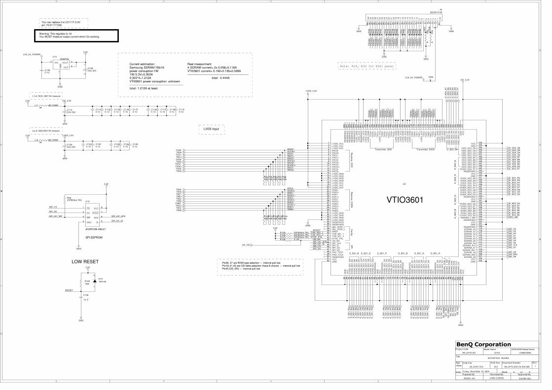
Current estimation:Samsung SDRAM 1Mx16power consuption:1W1W/3.3V=0.303A0.303*4=1.212AVTI03601 power consuption: unknown----------------------------------------------------------total: 1.212A at least
Real measurment:4 SDRAM current= 2x 0.058=0.116AVTI03601 current= 0.192+0.136=0.328A------------------------------------------------------------------ total: 0.444A
LOW RESET
U3
SPI EEPROM
LVDS Input
You can replace it to LD1117-3.3Vp/n: 74.01117.03C
Warning: This regulator is 1AYou MUST measure output current when ICs working
L2=0.136A 0621'04 measure
L1=0.192A, 0621'04 measure
Pin38, 37 are ROM type selection --- internal pull lowPin42,41,40 are OD table selection (have 8 choice) --- internal pull lowPin43 (OD_EN) --- internal pull low
Note: R29, R30 for EG01 panel
C1130.1U
R95100
R98100
R92
0
U12
AT25F512N-10SI-2.7
CS1
SO2
WP3
GND4 SI 5
SCK 6
HOLD 7
VCC 8
TP41 TP
37
TP54
R102100
C1220.1U
C126
1U Z
TP47
C1140.1U
J620D2013130
11
22
33
44
55
66
77
88
99
1010
1111
1212
1313
1414
1515
1616
1717
1818
1919
2020
G1
G1
G2
G2
2121
2222
2323
2424
2525
2626
2727
2828
2929
3030
TP48
L18 80 OHM3A
R10910K
TP42 TP
38
R94100
R105 OPEN(4.7K)
C1230.1U
R101100
+ C10822U 25V
12
TP49
C1150.1U
TP55
R99OPEN(4.7K)
C1240.1U
TP44
R100100
TP56
R106 OPEN(4.7K)
U10G960T63
GN
D1
VOUT 2VIN3
OUT 4
TP50
C1160.1U
+ C11022U 25V
12
TP59
TP57
TP39
R104100
C1250.1U
L17 80 OHM3A
R97100
C1170.1U
R91
0
C1090.1U
C1110.1U
R107 OPEN(4.7K)
D101N4148
12
TP45
TP58
C1180.1U
TP51
R96100
Receiver_O
DD
Receiver_E
VE
NC
onfigS
PI
E_SD1_B E_SD1_G E_SD1_R O_SD1_RO_SD1_GO_SD1_B
E_S
D2_
BE
_SD
2_G
E_S
D2_
RO
_SD
2_B
O_SD2_BRTransmitter_EVENTransmitter_ODD
VTIO3601
LVDS_VCC1
LVDS_VCC2
LVDS_VCC3
RXO0-4
RXO0+5
RXO1-6
RXO1+7
RXO2-8
RXO2+9
RXOC-10
RXOC+11
RXO3-12
RXO3+13
LVDS_GND14
LVDS_GND15
LVDS_GND16
LVDS_GND17
LVDS_VCC18
LVDS_VCC19
LVDS_VCC20
RXE0-21
RXE0+22
RXE1-23
RXE1+24
RXE2-25
RXE2+26
RXEC-27
RXEC+28
RXE3-29
RXE3+30
LVDS_GND31
LVDS_GND32
LVDS_GND33
LVDS_GND34
RESERVED35
RESERVED36
SEL_ROM_137
SEL_ROM_238
NRST39
TAB_SEL_140
TAB_SEL_241
NTSC_PAL42
OD_EN43
SPI_CLK44
SPI_SI45
SPI_CS46
SPI_SO47
PAD_TEST48
PAD_TCLK49
RESERVED50
VCC51
GND52
GN
D53
VC
C54
EV
EN
_SD
1_B
355
EV
EN
_SD
1_B
456
EV
EN
_SD
1_B
557
EV
EN
_SD
1_B
658
EV
EN
_SD
1_B
759
EV
EN
_SD
1_G
360
EV
EN
_SD
1_G
461
EV
EN
_SD
1_G
562
EV
EN
_SD
1_G
663
EV
EN
_SD
1_G
764
EV
EN
_SD
1_R
365
RE
SE
RV
ED
66
GN
D67
VC
C68
RE
SE
RV
ED
69
EV
EN
_SD
1_R
470
EV
EN
_SD
1_R
571
EV
EN
_SD
1_R
672
EV
EN
_SD
1_R
773
RE
SE
RV
ED
78
GN
D79
VC
C80
RE
SE
RV
ED
81
OD
D_S
D1_
B3
74
OD
D_S
D1_
B4
75
OD
D_S
D1_
B5
76
OD
D_S
D1_
B6
77
OD
D_S
D1_
B7
82
OD
D_S
D1_
G3
83
OD
D_S
D1_
G4
84
OD
D_S
D1_
G5
85
OD
D_S
D1_
G6
86
OD
D_S
D1_
G7
87
OD
D_S
D1_
R3
88
OD
D_S
D1_
R4
89
GN
D90
VC
C91
RE
SE
RV
ED
92
OD
D_S
D1_
R5
93
OD
D_S
D1_
R6
94
OD
D_S
D1_
R7
95
SD
RA
M_D
QM
_096
SD
RA
M_1
_WE
97
SD
RA
M_D
QM
_198
SD
RA
M_C
AS
99
SD
RA
M_R
AS
100
SD
RA
M_C
LK10
1
SD
RA
M_C
S10
2
GN
D10
3
VC
C10
4
GND 105VCC 106SDRAM_A9 107SDRAM_BA0 108SDRAM_A8 109SDRAM_BA1 110SDRAM_A7 111SDRAM_A10 112SDRAM_A6 113SDRAM_A0 114SDRAM_A5 115SDRAM_A1 116SDRAM_A4 117SDRAM_A2 118SDRAM_A3 119RESERVED 120GND 121VCC 122RESERVED 123SDRAM_2_WE 124EVEN_SD2_B3 125EVEN_SD2_B4 126EVEN_SD2_B5 127EVEN_SD2_B6 128EVEN_SD2_B7 129EVEN_SD2_G3 130GND 131VCC 132RESERVED 133EVEN_SD2_G4 134EVEN_SD2_G5 135EVEN_SD2_G6 136EVEN_SD2_G7 137EVEN_SD2_R3 138EVEN_SD2_R4 139EVEN_SD2_R5 140EVEN_SD2_R6 141GND 142VCC 143RESERVED 144EVEN_SD2_R7 145ODD_SD2_B3 146ODD_SD2_B4 147ODD_SD2_B5 148ODD_SD2_B6 149ODD_SD2_B7 150ODD_SD2_G3 151ODD_SD2_G4 152ODD_SD2_G5 153ODD_SD2_G6 154GND 155VCC 156
VC
C15
7G
ND
158
OD
D_S
D2_
G7
159
OD
D_S
D2_
R3
160
OD
D_S
D2_
R4
161
OD
D_S
D2_
R5
162
OD
D_S
D2_
R6
163
OD
D_S
D2_
R7
164
LVD
S_G
ND
165
LVD
S_V
CC
166
LVD
S_G
ND
167
LVD
S_G
ND
168
TX
E3+
169
TX
E3-
170
TX
EC
+17
1T
XE
C-
172
TX
E2+
173
TX
E2-
174
LVD
S_V
CC
175
TX
E1+
176
TX
E1-
177
TX
E0+
178
TX
E0-
179
LVD
S_G
ND
180
LVD
S_G
ND
181
LVD
S_V
CC
182
LVD
S_G
ND
183
LVD
S_V
CC
184
LVD
S_G
ND
185
LVD
S_G
ND
186
TX
O3+
187
TX
O3-
188
TX
OC
+18
9T
XO
C-
190
TX
O2+
191
TX
O2-
192
LVD
S_V
CC
193
TX
O1+
194
TX
O1-
195
TX
O0+
196
TX
O0-
197
LVD
S_G
ND
198
LVD
S_G
ND
199
LVD
S_V
CC
200
RE
SE
RV
ED
201
LVD
S_V
CC
202
LVD
S_G
ND
203
RE
SE
RV
ED
204
RE
SE
RV
ED
205
RE
SE
RV
ED
206
RE
SE
RV
ED
207
RE
SE
RV
ED
208
R103100
TP40
C1210.1U
TP52
R108 4.7K
C1120.1U
+ C12022U 25V
12
TP46
TP43
C1190.1U
TP53

5
5
4
4
3
3
2
2
1
1
D D
C C
B B
A A
D_O_SD2_R3
D_O_SD2_G6
D_O_SD2_R4
D_O_SD2_G7
D_E
_SD
2_G
5D
_E_S
D2_
G4
D_E
_SD
2_B
6
D_E
_SD
2_B
7D
_E_S
D2_
G3
SD_D
QM
1
D_E
_SD
2_B
3D
_E_S
D2_
B4
D_E
_SD
2_B
5
SD
_RA
S
SD2_
WE
SD
_CS
SD
_CA
S
SD_A
0SD
_A10
SD_B
A0
SD_A
1
D_E
_SD
2_G
7
D_E
_SD
2_G
6
SD_A
3SD
_A2
D_E
_SD
2_R
3
D_E
_SD
2_R
6
D_E
_SD
2_R
5D
_E_S
D2_
R4
SD_A
9
SD_D
QM
1SD
RA
M_C
LO
CK
D_E
_SD
2_R
7
SD_A
6SD
_A7
SD_A
8
SD_A
5SD
_A4
D_O
_SD
2_G
4D
_O_S
D2_
G5
D_O
_SD
2_B
7D
_O_S
D2_
G3
D_O
_SD
2_B
6
D_O
_SD
2_B
4
D_O
_SD
2_B
5
D_O
_SD
2_B
3
SD
_RA
S
SD_D
QM
1
SD
_CA
SSD
2_W
E
SD_B
A0
SD_A
10SD
_A0
SD
_CS
SD_A
2
D_O
_SD
2_G
6
SD_A
1
SD_A
3
D_O
_SD
2_R
4
D_O
_SD
2_R
3
D_O
_SD
2_R
5
D_O
_SD
2_G
7
SD_D
QM
1SD
RA
M_C
LO
CK
D_O
_SD
2_R
7D
_O_S
D2_
R6
SD_A
9SD
_A8
SD_A
6SD
_A7
SD_A
5SD
_A4
D_E
_SD
1_B
4D
_E_S
D1_
B3
D_E
_SD
1_R
6
D_E
_SD
1_R
3
D_E
_SD
1_B
7
D_E
_SD
1_R
5
D_E
_SD
1_G
6D
_E_S
D1_
G7
D_E
_SD
1_G
4
D_E
_SD
1_B
6
D_E
_SD
1_R
4
D_E
_SD
1_G
5
D_E
_SD
1_G
3
D_E
_SD
1_B
5
D_E
_SD
1_R
7
D_O
_SD
1_R
7
D_O
_SD
1_R
5
D_O
_SD
1_B
6
D_O
_SD
1_B
3
D_O
_SD
1_G
7
D_O
_SD
1_G
4
D_O
_SD
1_R
4
D_O
_SD
1_B
5
D_O
_SD
1_G
3
D_O
_SD
1_R
3
D_O
_SD
1_B
4
D_O
_SD
1_G
6
D_O
_SD
1_B
7
D_O
_SD
1_R
6
D_O
_SD
1_G
5
SDRAM_CLOCK
D_O_SD1_B4
D_O_SD1_B5
D_O_SD1_B3
D_O_SD1_G4
D_O_SD1_B6
D_O_SD1_B7D_O_SD1_G3
D_O_SD1_G5
SD1_WESD_CAS
SD_DQM0
SD_BA0SD_CS
SD_A10
SD_RAS
SD_A3
SD_A1SD_A0
SD_A2
D_O_SD1_R7
D_O_SD1_R6
D_O_SD1_R4
D_O_SD1_R5
SD_DQM0
D_O_SD1_G6
D_O_SD1_R3
D_O_SD1_G7
SD_A7SD_A8
SDRAM_CLOCK
SD_A9
SD_A5SD_A4
SD_A6
D_E_SD1_B3D_E_SD1_B4
D_E_SD1_B7D_E_SD1_G3
D_E_SD1_B5D_E_SD1_B6
SD_DQM0SD1_WE
D_E_SD1_G4D_E_SD1_G5
SD_RASSD_CAS
SD_CSSD_BA0
SD_A1SD_A2
SD_A10SD_A0
D_E_SD1_R6
SD_A3
D_E_SD1_R7
D_E_SD1_R5
D_E_SD1_R4
D_E_SD1_G6D_E_SD1_G7
D_E_SD1_R3
SD_DQM0
SD_A8SD_A9
SDRAM_CLOCK
SD_A7SD_A6SD_A5SD_A4
D_E_SD2_R7D_E_SD2_R6D_E_SD2_R5
D_E_SD2_R4D_E_SD2_R3D_E_SD2_G7D_E_SD2_G6
D_E_SD2_G5D_E_SD2_G4D_E_SD2_G3D_E_SD2_B7
D_E_SD2_B6D_E_SD2_B5D_E_SD2_B4D_E_SD2_B3
D_O_SD2_B3
D_O_SD2_R5
D_O_SD2_R7D_O_SD2_R6
D_O_SD2_G5D_O_SD2_G4D_O_SD2_G3D_O_SD2_B7
D_O_SD2_B6D_O_SD2_B5D_O_SD2_B4
SDRAM2_3.3V
SDRAM2_3.3V
SDRAM1_3.3V SDRAM1_3.3V
3.3V
3.3V
SDRAM1_3.3V
SDRAM2_3.3V
GND
GND
GNDGND
GND
GND
E_S
D1_
B3
E_S
D1_
B4
E_S
D1_
B5
E_S
D1_
B6
E_S
D1_
B7
E_S
D1_
G3
E_S
D1_
G4
E_S
D1_
G5
E_S
D1_
G6
E_S
D1_
G7
E_S
D1_
R3
E_S
D1_
R4
E_S
D1_
R5
E_S
D1_
R6
E_S
D1_
R7
O_S
D1_
B3
O_S
D1_
B4
O_S
D1_
B5
O_S
D1_
B6
O_S
D1_
B7
O_S
D1_
G3
O_S
D1_
G4
O_S
D1_
G5
O_S
D1_
G6
O_S
D1_
G7
O_S
D1_
R3
O_S
D1_
R4
O_S
D1_
R5
O_S
D1_
R6
O_S
D1_
R7
O_SD2_R7O_SD2_R6O_SD2_R5
O_SD2_R4O_SD2_R3O_SD2_G7O_SD2_G6
O_SD2_G5O_SD2_G4O_SD2_G3O_SD2_B7
O_SD2_B6O_SD2_B5O_SD2_B4O_SD2_B3
E_SD2_R7E_SD2_R6E_SD2_R5
E_SD2_R4E_SD2_R3E_SD2_G7E_SD2_G6
E_SD2_G5E_SD2_G4E_SD2_G3E_SD2_B7
E_SD2_B6E_SD2_B5E_SD2_B4E_SD2_B3
SD_CLK
SD_A3SD_A2SD_A4SD_A1SD_A5SD_A0SD_A6SD_A10SD_A7
SD_A8SD_BA0SD_A9
SD_DQM0SD1_WE
SD_DQM1SD_CASSD_RAS
SD_CS
SD2_WE
Title
Size Document Number R e v.
Date: Sheet o f
Project Code
Reviewed By Approved ByPrepared By
Model Name
PCB P/N PCB Rev.
��������������OEM/ODM Model Name
99.L0Y72.000-C3-304-006
INTERFACE BOARD
6 6
LINIX CHENG DAVEN WU
48.L0Y01.S12 S12
ANGEL HU
<Size>
Q7C499.L0Y72.001
1
Friday, November 19, 2004
<OEM/ODM>
If bead array is too small (now is 0805),you can change to 1206 (use p/n:68.12160.AQ1)
L3=0.058A 0621'04measure
L4=0.058A 0621'04 measure
C1370.1U
C1290.1U
C1470.1U
U15
K4S161622E-TC70
VDD1
DQ02
DQ13
VSSQ4
DQ25
DQ36
VDDQ7
DQ48
DQ59
VSSQ10
DQ611
DQ712
VDDQ13
LDQM14
WE15
CAS16
RAS17
CS18
BA19
A10/AP20
A021
A122
A223
A324
VDD25 VSS 26A4 27A5 28A6 29A7 30A8 31A9 32NC 33
CKE 34CLK 35
UDQM 36NC/RFU 37
VDDQ 38DQ8 39DQ9 40
VSSQ 41DQ10 42DQ11 43VDDQ 44DQ12 45DQ13 46VSSQ 47DQ14 48DQ15 49
VSS 50
C1410.1U
C1520.1U
+ C12722U 25V
12
RN70
1234
8765
C1380.1U
RN100
1234
8765
RN5 01234
8765
C1300.1U
U13K4S161622E-TC70
VD
D1
DQ
02
DQ
13
VS
SQ
4
DQ
25
DQ
36
VD
DQ
7
DQ
48
DQ
59
VS
SQ
10
DQ
611
DQ
712
VD
DQ
13
LDQ
M14
WE
15
CA
S16
RA
S17
CS
18
BA
19
A10
/AP
20
A0
21
A1
22
A2
23
A3
24
VD
D25
VS
S26
A4
27A
528
A6
29A
730
A8
31A
932
NC
33C
KE
34C
LK35
UD
QM
36N
C/R
FU
37V
DD
Q38
DQ
839
DQ
940
VS
SQ
41D
Q10
42D
Q11
43V
DD
Q44
DQ
1245
DQ
1346
VS
SQ
47D
Q14
48D
Q15
49V
SS
50
L19 80 OHM3A
RN120
1234
8765
C1310.1U
+ C14222U 25V
12
C1530.1U
C1390.1U
C1480.1U
L20 80 OHM3A
RN14 01234
8765
R110 0
RN2 01234
8765
C1450.1U
C1320.1U
RN80
1234
8765
RN1 01234
8765
C1540.1U
C1490.1U
C1330.1U
C1460.1U
C1550.1U
C1400.1U
RN15 01234
8765
RN3 01234
8765
C1340.1U
RN110
1234
8765
C1560.1U
C1500.1U
C1350.1U
RN60
1234
8765
RN90
1234
8765
C1430.1U
U16
K4S161622E-TC70
VDD1
DQ02
DQ13
VSSQ4
DQ25
DQ36
VDDQ7
DQ48
DQ59
VSSQ10
DQ611
DQ712
VDDQ13
LDQM14
WE15
CAS16
RAS17
CS18
BA19
A10/AP20
A021
A122
A223
A324
VDD25 VSS 26A4 27A5 28A6 29A7 30A8 31A9 32NC 33
CKE 34CLK 35
UDQM 36NC/RFU 37
VDDQ 38DQ8 39DQ9 40
VSSQ 41DQ10 42DQ11 43VDDQ 44DQ12 45DQ13 46VSSQ 47DQ14 48DQ15 49
VSS 50
C1280.1U
RN4 01234
8765
C1510.1U
C1360.1U
RN16 01234
8765
RN130
1234
8765
U14K4S161622E-TC70
VD
D1
DQ
02
DQ
13
VS
SQ
4
DQ
25
DQ
36
VD
DQ
7
DQ
48
DQ
59
VS
SQ
10
DQ
611
DQ
712
VD
DQ
13
LDQ
M14
WE
15
CA
S16
RA
S17
CS
18
BA
19
A10
/AP
20
A0
21
A1
22
A2
23
A3
24
VD
D25
VS
S26
A4
27A
528
A6
29A
730
A8
31A
932
NC
33C
KE
34C
LK35
UD
QM
36N
C/R
FU
37V
DD
Q38
DQ
839
DQ
940
VS
SQ
41D
Q10
42D
Q11
43V
DD
Q44
DQ
1245
DQ
1346
VS
SQ
47D
Q14
48D
Q15
49V
SS
50
C1440.1U


![Welcome [static.highspeedbackbone.net]static.highspeedbackbone.net/pdf/benq-fp222wb-manual.pdfHave Disk button, insert the BenQ LCD Monitor CD-ROM and select the appropriate monitor](https://static.fdocuments.in/doc/165x107/5aab515c7f8b9a9c2e8bc275/welcome-disk-button-insert-the-benq-lcd-monitor-cd-rom-and-select-the-appropriate.jpg)