BD9478F : LED / LCD Drivers -...
15
Product structure Silicon monolithic integrated circuit This product is not designed protection against radioactive rays . 1/12 TSZ02201-0F1F0C100010-1-2 © 2012 ROHM Co., Ltd. All rights reserved. 24. Jul.2012 Rev.002 TSZ22111 14 001 www.rohm.com LED Drivers series for LCD Backlights PWM pulse Generator for LCD Panels BD9478F General Description BD9478F is PWM pulse generator for LCD panel. This IC compares triangle waveform which is generated inside IC and external DC signal, and generates a PWM pulse. This PWM pulse is provided to LED driver and controls LED grayscale. PWM pulse frequency can be synchronized to external signal frequency inputted to SYNC terminal. Even if this frequency gets out of range, it works in the setting frequency, is protected and it always provides stable PWM pulse to LED driver. Key Specification Operating power supply voltage range: 4.5V to 5.5V Free Run frequency: 150Hz (CT=0.01μF) Operating Current: 2mA (typ.) Operating temperature range: -40 to +85 Applications LED backlight of monitor, TV, NOTE PC, etc. Features The signal that the frequency synchronizes with the VSYNC signal is output to PWMOUT. The PWM pulse is generated with the DC signal of a triangular wave and PDIM generated with the LCT capacitor. When the VSYNC frequency exceeds the stipulated range, it fixes by a set frequency. (fSYNC<fPLLtyp*0.35 -> fPLL=0.36*fPLLtyp , fSYNC> fPLLtyp*2.75 -> fPLL=2.75*fPLLtyp) When VSYNC is a no signal input, the self-oscillation is operated by set frequency decided on the CT capacitance. When the pulse signal is input to the terminal EXTPWM, it shifts automatically to external PWM mode. Package W(Typ.) D(Typ.) H(Max.) SOP-8: 5.00mm x 6.20mm x 1.71mm Pin Pitch: 1.27mm Typical Application Circuit Figure 2. Typical Application Circuit Figure 1. SOP-8 Not Recommended for New Designs
Transcript of BD9478F : LED / LCD Drivers -...
Product structure:Silicon monolithic integrated circuit This product is not designed protection against radioactive rays .
1/12 TSZ02201-0F1F0C100010-1-2
© 2012 ROHM Co., Ltd. All rights reserved.
24. Jul.2012 Rev.002TSZ22111・14・001 www.rohm.com
Datasheet
1234 5678 CLPF1 CLPF2CCT
PWM signal out(to LED driver)CVCCCEXTPWMCPDIMCVSYNCConnector
VINPDIMfVSYNC RLPF2VCCEXTPWMPDIMVSYNC
PWMOUTGNDLPFCT
LED Drivers series for LCD Backlights
PWM pulse Generator for LCD Panels BD9478F General Description
BD9478F is PWM pulse generator for LCD panel. This IC compares triangle waveform which is generated inside IC and external DC signal, and generates a PWM pulse. This PWM pulse is provided to LED driver and controls LED grayscale. PWM pulse frequency can be synchronized to external signal frequency inputted to SYNC terminal. Even if this frequency gets out of range, it works in the setting frequency, is protected and it always provides stable PWM pulse to LED driver. Key Specification
Operating power supply voltage range: 4.5V to 5.5V Free Run frequency: 150Hz (CT=0.01µF) Operating Current: 2mA (typ.)
Operating temperature range: -40 to +85
Applications
LED backlight of monitor, TV, NOTE PC, etc.
Features The signal that the frequency synchronizes with the VSYNC signal is output to PWMOUT. The PWM pulse is generated with the DC signal of a triangular wave and PDIM generated with the LCT capacitor. When the VSYNC frequency exceeds the stipulated range, it fixes by a set frequency. (fSYNC<fPLLtyp*0.35 -> fPLL=0.36*fPLLtyp , fSYNC> fPLLtyp*2.75 -> fPLL=2.75*fPLLtyp) When VSYNC is a no signal input, the self-oscillation is operated by set frequency decided on the CT capacitance. When the pulse signal is input to the terminal EXTPWM, it shifts automatically to external PWM mode. Package W(Typ.) D(Typ.) H(Max.)
SOP-8: 5.00mm x 6.20mm x 1.71mm Pin Pitch: 1.27mm
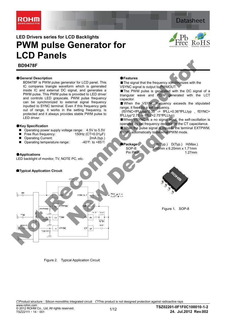
Typical Application Circuit
Figure 2. Typical Application Circuit
Figure 1. SOP-8
Not R
ecom
men
ded
for
New D
esig
ns

2/12
DatasheetBD9478F
TSZ02201-0F1F0C100010-1-2© 2012 ROHM Co., Ltd. All rights reserved. 24. Jul.2012 Rev.002
www.rohm.com
TSZ22111・15・001
Absolute maximum ratings (Ta=25) Parameter Symbol Ratings Unit
Power supply voltage VCC 7 V
Operating Temperature Range Ta(opr) -40 ~ +85 °C
Storage Temperature Range Tstg -55 ~ +150 °C
Junction Temperature Tjmax 150 °C
Power Dissipation Pd 689※1 mW *1 Decreases 5.5mW/°C at Ta=25°C or higher (When mounting a one-layer 70.0mmx70.0mmx1.6mm board)
Operating Ratings (Ta = 25)
Parameter Symbol Range Unit
Power supply voltage VCC 4.5 ~ 5.5 V
VSYNC input frequency range F_VSYNC 0.040 ~ 0.8 kHz
EXTPWM input PWM signal frequency range F_EXTPWM FCT ~ 30 kHz The operating conditions written above are constants of the IC unit. Be careful enough when setting the constant in the actual set. FCT is dimming frequency that oscillates itself when VSYNC terminal is input no signal
External Components Recommended Range
Item Symbol Setting Range Unit
VCC capacitance CVCC 0.1 ~ 10 µF
PLL Burst OSC oscillation frequency setting capacitance CT 0.040 ~ 0.8 µF
The operating conditions written above are constants of the IC unit. Be careful enough when setting the constant in the actual set.
Pin Configuration Marking diagram and physical dimension
SOP-8
Figure 3. Pin Configuration Figure 4. Physical Dimension
1 2 3 4
5678
VCC
EXTPWM
PDIM
VSYNC
PWMOUT
GND
LPF
CT
Lot No.
D9478
Not R
ecom
men
ded
for
New D
esig
ns

3/12
DatasheetBD9478F
TSZ02201-0F1F0C100010-1-2© 2012 ROHM Co., Ltd. All rights reserved. 24. Jul.2012 Rev.002
www.rohm.com
TSZ22111・15・001
Electrical Characteristics (Unless otherwise specified, Ta=25°C,VCC=5V)
Parameter Symbol Limit
Unit Condition Min. Typ. Max.
[Whole Device]
Circuit Current during Operation ICC ― 2 4 mA PDIM=3V,CT=0.01uF
VSYNC=EXTPWM=open
[UVLO Block]
Release voltage VUVLO 3.5 3.8 4.1 V VCC=SWEEP UP
Hysteresis voltage VUHYS 150 300 600 mV VCC=SWEEP DOWN
[PLL Block]
Oscillation frequency when VSYNC is
input no signal fCTNS 142 150 158 Hz CT=0.01µF,LPF=0V
Triangle wave maximum voltage VCTH 2.70 3.00 3.30 V fCT=150Hz
Triangle wave minimum voltage VCTL 0.40 0.50 0.60 V fCT=150Hz
Synchronous signal abnormal judgment voltage, (at High frequency input)
CT_SYNC _DET1 2.612 2.750 2.888 V LPF=2.0V→3.0V
Synchronous signal normal judgment voltage, (at High frequency input)
CT_SYNC _OKH 2.517 2.650 2.783 V LPF=3.0V→2.0V
Internal RT voltage at Synchronous signal, abnormal judgment when High frequency input VRTFH - 2.750 - V LPF=3V
Synchronous signal abnormal judgment voltage, (at Low frequency input)
CT_SYNC _DET2 0.331 0.350 0.389 V LPF=1.0V→0.1V
Synchronous signal normal judgment voltage, (at Low frequency input)
CT_SYNC _OKL 0.414 0.450 0.486 V LPF=0.1V→1.0V
Internal RT voltage at Synchronous signal, abnormal judgment when High frequency input VRTFL - 0.360 - V LPF=0.25V
Switch voltage to internal fixed frequency VINTF 0.10 0.15 0.20 V LPF=1.0V→0.1V
Internal RT voltage at switched to internal fixed, frequency VRTFI - 0.900 - V LPF=0V 【【【【Input pin (EXTPWM,PDIM,VSYNC)】】】】 Input High level VIH 2.0 - 20 V
Input Low level VIL -0.3 - 0.8 V
Pull down resistance RIPD 0.5 1.0 2.0 MΩ 【【【【Output pin (PWMOUT)】】】】 Output High level VOH 4.3 4.85 - V Io=-1mA
Output Low level VOL - 0.1 0.5 V Io=1mA
Not R
ecom
men
ded
for
New D
esig
ns

4/12
DatasheetBD9478F
TSZ02201-0F1F0C100010-1-2© 2012 ROHM Co., Ltd. All rights reserved. 24. Jul.2012 Rev.002
www.rohm.com
TSZ22111・15・001
Pin Descriptions
Pin No Pin Name In/Out Function Rating [V]
1 VCC - Power supply -0.3~7
2 EXTPWM In External PWM signal input -0.3~20
3 PDIM In DC signal input for Internal PWM -0.3~20
4 VSYNC In Synchronous signal input -0.3~20
5 CT Out Capacitance pin for VCO -0.3~7
6 LPF In/Out LPF output for PLL -0.3~7
7 GND - Ground -
8 PWMOUT Out PWM dimming signal output -0.3~7
Pin ESD Type
VCC EXTPWM / VSYNC /PDIM CT
VCC
CT
7V
LPF GND PWMOUT
Figure 5. Pin ESD Type
Not R
ecom
men
ded
for
New D
esig
ns

5/12
DatasheetBD9478F
TSZ02201-0F1F0C100010-1-2© 2012 ROHM Co., Ltd. All rights reserved. 24. Jul.2012 Rev.002
www.rohm.com
TSZ22111・15・001
Block Diagram
PhaseComparetor +-+-f×0.35f×0.15 VoltageControlledOscillatorselectorFrequency lock comparator
+-PWM comparatorVSYNCGNDVCC
LPF CT PDIMPWMOUT
Loop Filter DCsignalPulse signal selector
EXTPWM +-f×2.75
Figure 6. Block Diagram
Not R
ecom
men
ded
for
New D
esig
ns

6/12
DatasheetBD9478F
TSZ02201-0F1F0C100010-1-2© 2012 ROHM Co., Ltd. All rights reserved. 24. Jul.2012 Rev.002
www.rohm.com
TSZ22111・15・001
Typical Performance Curve
0
100
200
300
400
500
0 5 10 15 20
CCT [nF]frequency fCT [Hz]
0.0
0.5
1.0
1.5
2.0
2.5
3.0
3.5
4.0
100 150 200 250 300 350 400
fCT [Hz]
PWMOUT jitter [us]
0
20
40
60
80
100
120
0 1 2 3 4
PDIM [V]
PWM DUTY [%]
0
1
2
3
4
4.0 4.5 5.0 5.5 6.0
VCC [V]
Operating current ICC [mA]
Figure 7. Operating Current (ICC) [mA] vs. VCC[V] Figure 8. frequency fCT[Hz] vs. CT[nF]
Figure 9. PWM DUTY [%] vs. PDIM[V]
Figure 11. Start up waveform (Free Run mode) Figure 12. EXTPWM mode waveform
Figure 10. PWMOUT jitter [µs] vs. fCT[Hz]
CT
PDIM
EXTPWM
PWMOUT
f-200Hz
PWMOUT
CT
PDIM
VCC Not
Rec
omm
ende
d fo
r
New D
esig
ns

7/12
DatasheetBD9478F
TSZ02201-0F1F0C100010-1-2© 2012 ROHM Co., Ltd. All rights reserved. 24. Jul.2012 Rev.002
www.rohm.com
TSZ22111・15・001
Pin Function
Pin 1: VCC
Power supply pin of the IC. Input range is from 4.5V to 5.5V
Operation starts at VCC=3.8V(TYP.) or higher and shuts down at VCC=3.5V(TYP.) or lower.
Pin 2: EXTPWM
External PWM signal input terminal. In case of the following equation, the signal input to EXTPWM is output directly to PWMOUT. The equation ; f(PLL) < 2 * f(EXTPWM) f(EXTPWM) ; frequency of signal input to EXTPWM f(PLL) ; frequency of signal that synchronizes with VSYNC signal
Pin 3: PDIM
DC signal input terminal to generate internal PWM signal. The PWM signal is generated with compare it with a triangular waveform in IC. If PDIM input DC level is changed, PWM Duty can be changed. PDIM input DC voltage range is from 0.5V to 3.0V. (PWM Duty is changed from 0% to 100%)
Pin 4: VSYNC
Synchronous signal input terminal. The signal that synchronizes with the frequency of the signal input to VSYNC is generated with PLL. A triangular wave is generated based on the frequency of this synchronized signal, and the PWM pulse is generated with compare it with the PDIM signal
Pin 5: CT
Capacitor connection terminal that decides the oscillation frequency of VCO.. Please adjust the capacity of CT by the following equation so that the voltage of the terminal LPF may become 0.9V when the frequency of the signal that synchronizes is input.
Pin 6: LPF
Low pass filter connection pin. The pulse signal output from Phase Comparator is smoothed by Low path filter, and it inputs to Voltage. Controlled Oscillator (VCO).
Pin 7: GND
Ground pin of this IC. Pin 8: PWMOUT
PWM signal output pin. The PWM signal generated in IC is output.
][ ][
5.1uF
HzfCT
PLLtyp
=
Not R
ecom
men
ded
for
New D
esig
ns

8/12
DatasheetBD9478F
TSZ02201-0F1F0C100010-1-2© 2012 ROHM Co., Ltd. All rights reserved. 24. Jul.2012 Rev.002
www.rohm.com
TSZ22111・15・001
About Dimming Function Burst Frequency Free Run Function
Because PLL is incorporated, Free Run operation is possible for burst frequency. PLL circuit will operate like it synchronizes with the frequency of signal input to VSYNC pin. Then, the voltage that is in proportion to the frequency will be generated in LPF pin. When LPF pin voltage becomes 0.35V or lower, it will judge the external burst frequency is abnormal and clumps with the frequency of fPLLmin. Then, PLL frequency is changed to Free Run frequency. (note1) When the burst frequency becomes normal and LPF pin becomes over 0.9V, it will return to the state that synchronizes with the burst frequency.(note2) In the same way, when LPF pin becomes 2.75V or more, it will clump with the frequency of fPLLmax. When the burst frequency becomes normal and LPF2 pin becomes 2.65V or lower, it will return to the state that synchronizes with the burst frequency. When LPF pin becomes 0.15V or lower, it will judge the external burst frequency is not inputted and switches to the frequency of fPLLtyp.(Free Run mode)
Note1
If fVSYNC is less than fPLLmin, the input of VCO is fixed to 0.36V inside IC, and PWM frequency is fixed to fPLLmin. However, since it is fVSYNC<fPLLmin, a LPF terminal approaches 0V. Then, it is set to LPF<0.15V, and it shifts to Free Run mode and PWM frequency is set to fPLLtyp.
Note2 In order to shift to PLL mode, it is necessary to input bigger frequency than Free Run frequency into VSYNC.
Figure 13.
Not R
ecom
men
ded
for
New D
esig
ns

9/12
DatasheetBD9478F
TSZ02201-0F1F0C100010-1-2© 2012 ROHM Co., Ltd. All rights reserved. 24. Jul.2012 Rev.002
www.rohm.com
TSZ22111・15・001
LPF2Voltage
(Free Run Operation Explanation)
For example, if you set CT=0.01uF (At this time, fPLLtyp is adjusted to 150 Hz.) and f(VSYNC)=180Hz, the LPF pin voltage becomes 1.2V. The built-in VCO is proportional to the LPF pin voltage. If VSYNC is inputted to low frequency and it becomes LPF<0.35V (at this time, f<58Hz),it will clump at fPLLmin=58Hz. However, since it is fVSYNC<fPLLmin, a LPF terminal approaches 0V. Then, it is set to LPF<0.15V, and it shifts to Free Run mode and PWM frequency is set to fPLLtyp. (at this time, f=150Hz).If fSYNC is larger than fPLLtyp, PWM frequency will return to the frequency that synchronizes with f(VSYNC). If VSYNC is inputted high frequency and it becomes LPF>2.75V (at this time, f>343Hz),it will clump at fPLLmax=343Hz. When synchronous signal is not inputted to VSYNC terminal, LPF voltage decreases and then it becomes LPF<0.15V (at this time, f<19Hz), it oscillates typical frequency (at this time, f=150Hz). Note: Please set f(VSYNC) frequency to satisfy the following equations when you start up PLL mode. And then, please change f(VSYNC) frequency. f(VSYNC) > fPLLtyp , fPLLtyp = 1.5/(CT[uF]) [Hz]
Figure 14.
Not R
ecom
men
ded
for
New D
esig
ns

10/12
DatasheetBD9478F
TSZ02201-0F1F0C100010-1-2© 2012 ROHM Co., Ltd. All rights reserved. 24. Jul.2012 Rev.002
www.rohm.com
TSZ22111・15・001
Dimming Signal Automatic Selection Function
In this IC, even if either PWM dimming signal or DC dimming signal is inputted into the DUTY pin, it is automatically distinguished as DC or PWM in the IC. By detecting 4 cycles of the PWM signal within the 8 cycles of the burst frequency in the IC, it will switch automatically
to PWM dimming. Therefore, set the burst frequency in the IC as follows:
(Burst Frequency in the IC(same fSYNC)) < 2 X (Externally inputted PWM signal (fEXTPWM)) Also, if you do not detect 4 cycles of the PWM signal within the 8 cycles of the burst frequency after switching to PWM dimming, it will automatically switch to DC dimming.
(a) When (Burst Frequency in the IC) < 2 X (Externally inputted PWM signal)
(b)When (Burst Frequency in the IC ) ≧ 2 X (Externally inputted PWM signal)
Burst frequency in the IC
Burst FF output in the IC
Externally inputted PWM signal
Output dimming signal
Burst frequency 8 cycles
PWM signal 4 cycles
Output comparator of triangle wave and PWM signal
PWM dimming output
Burst frequency in the IC
Burst FF output in the IC
External PWM signal
Burst dimming signal
Burst frequency 8 cycles
PWM signal 4 cycles
Output comparator of triangle wave and PWM signal
Figure 15.
Figure 16. Not R
ecom
men
ded
for
New D
esig
ns

11/12
DatasheetBD9478F
TSZ02201-0F1F0C100010-1-2© 2012 ROHM Co., Ltd. All rights reserved. 24. Jul.2012 Rev.002
www.rohm.com
TSZ22111・15・001
Operational Notes
1.) Although the quality of this product has been tightly controlled, deterioration or even destruction may occur if the absolute maximum
ratings, such as for applied pressure and operational temperature range, are exceeded. Furthermore, we are unable to assume short
or open mode destruction conditions. If special modes which exceed the absolute maximum ratings are expected, physical safely
precautions such as fuses should be considered.
2.) The IC can destruct from reverse connection of the power supply connector. Precautions, such as inserting a diode between t
he external power supply and IC power terminal, should be taken as protection against reverse connection destruction.
3.) When attaching to the printed substrate, pay special attention to the direction and proper placement of the IC. If the IC is att
ached incorrectly, it may be destroyed.
Destruction can also occur when there is a short, which can be caused by foreign objects entering between outputs or an output and the
power GND.
4.) Because there is a return of current regenerated by back EMF of the external coil, the capacity value should be determined af
ter confirming that there are no problems with characteristics such as capacity loss at low temperatures with electrolysis conde
nsers, for example by placing a condenser between the power supply and GND as a route for the regenerated current.
5.) The potential of the GND pin should be at the minimum potential during all operation status
6.) Heat design should consider power dissipation (Pd) during actual use and margins should be set with plenty of room.
7.) Exercise caution when operating in strong magnet fields, as errors can occur.
8.) When using this IC, it should be configured so that the output Tr should not exceed absolute maximum ratings and ASO. Wit
h CMOS ICs and ICs which have multiple power sources, there is a chance of rush current flowing momentarily, so exercise c
aution with power supply coupling capacity, power supply and width of GND pattern wiring and its layout.
9.) This IC has a built-in Temperature Protection Circuit (TSD circuit). The temperature protection circuit (TSD circuit) is only to cut off the IC from thermal runaway, and has not been designed to protect or guarantee the IC. Therefore, the user should not plan to activate this circuit with continued operation in mind.
10.) If a condenser is connected to a pin with low impedance when inspecting the set substrate, stress may be placed on the IC,
so there should be a discharge after each process. Furthermore, when connecting a jig for the inspection process, the power
must first be turned OFF before connection and inspection, and turned OFF again before removal.
11.) This IC is a monolithic IC, and between each element there is a P+ isolation and P substrate for element separation. There is a P-N junction formed between this P-layer and each element’s N-layer, which makes up various parasitic elements. For example, when resistance and transistor are connected with a terminal as in figure 15: When GND>(terminal A) at the resistance, or GND>(terminal B) at the transistor (NPN), the P-N junction operates as a parasitic diode. Also, when GND>(terminal B) at the transistor, a parasitic NPN transistor operates by the N-layer of other elements close to the aforementioned parasitic diode.
With the IC’s configuration, the production of parasitic elements by the relationships of the electrical potentials is inevitable. The operation of the parasitic elements can also interfere with the circuit operation, leading to malfunction and even destruction. Therefore, uses which cause the parasitic elements to operate, such as applying voltage to the input terminal which is lower than the GND (P-substrate), should be avoided.
Status of this document The Japanese version of this document is formal specification. A customer may use this translation version only for a reference to help reading the formal version.
If there are any differences in translation version of this document formal version takes priority
Figure 17. Example of Simple Structure of Monolithic IC
GND BC
E
Adjacent other elements Parasitic
(Pin B) GND
Parasitic element
(Pin A)
Parasitic element
Resistor
P substrate
N
GND
P
N
P
(Pin A)
PN
Transistor (NPN)
B
Parasitic element
GND
E C
GND
P P
N
N
N
P
N
P substrate
(Pin B)
Not R
ecom
men
ded
for
New D
esig
ns

12/12
DatasheetBD9478F
TSZ02201-0F1F0C100010-1-2© 2012 ROHM Co., Ltd. All rights reserved. 24. Jul.2012 Rev.002
www.rohm.com
TSZ22111・15・001
Ordering Information
B D 9 4 7 8 F - XX
Part Number Package F:SOP
Packaging and forming specification XX: Please confirm the formal name to our sales.
Physical Dimension Tape and Reel Information
∗ Order quantity needs to be multiple of the minimum quantity.
<Tape and Reel information>
Embossed carrier tapeTape
Quantity
Direction
of feedThe direction is the 1pin of product is at the upper left when you hold
reel on the left hand and you pull out the tape on the right hand
2500pcs
E2
( )
Direction of feed
Reel1pin
(Unit : mm)
SOP8
0.9
±0.1
5
0.3
MIN
4°+6°−4°
0.17+0.1-0.05
0.595
6
43
8
2
5
1
7
5.0±0.2
6.2
±0.3
4.4
±0.2
(MAX 5.35 include BURR)
1.27
0.1
1
0.42±0.1
1.5
±0.1
S
0.1 S
Not R
ecom
men
ded
for
New D
esig
ns

DatasheetDatasheet
Notice - GE Rev.002© 2014 ROHM Co., Ltd. All rights reserved.
Notice Precaution on using ROHM Products
1. Our Products are designed and manufactured for application in ordinary electronic equipments (such as AV equipment, OA equipment, telecommunication equipment, home electronic appliances, amusement equipment, etc.). If you intend to use our Products in devices requiring extremely high reliability (such as medical equipment (Note 1), transport equipment, traffic equipment, aircraft/spacecraft, nuclear power controllers, fuel controllers, car equipment including car accessories, safety devices, etc.) and whose malfunction or failure may cause loss of human life, bodily injury or serious damage to property (“Specific Applications”), please consult with the ROHM sales representative in advance. Unless otherwise agreed in writing by ROHM in advance, ROHM shall not be in any way responsible or liable for any damages, expenses or losses incurred by you or third parties arising from the use of any ROHM’s Products for Specific Applications.
(Note1) Medical Equipment Classification of the Specific Applications JAPAN USA EU CHINA
CLASSⅢ CLASSⅢ
CLASSⅡb CLASSⅢ
CLASSⅣ CLASSⅢ
2. ROHM designs and manufactures its Products subject to strict quality control system. However, semiconductor
products can fail or malfunction at a certain rate. Please be sure to implement, at your own responsibilities, adequate safety measures including but not limited to fail-safe design against the physical injury, damage to any property, which a failure or malfunction of our Products may cause. The following are examples of safety measures:
[a] Installation of protection circuits or other protective devices to improve system safety [b] Installation of redundant circuits to reduce the impact of single or multiple circuit failure
3. Our Products are designed and manufactured for use under standard conditions and not under any special or extraordinary environments or conditions, as exemplified below. Accordingly, ROHM shall not be in any way responsible or liable for any damages, expenses or losses arising from the use of any ROHM’s Products under any special or extraordinary environments or conditions. If you intend to use our Products under any special or extraordinary environments or conditions (as exemplified below), your independent verification and confirmation of product performance, reliability, etc, prior to use, must be necessary:
[a] Use of our Products in any types of liquid, including water, oils, chemicals, and organic solvents [b] Use of our Products outdoors or in places where the Products are exposed to direct sunlight or dust [c] Use of our Products in places where the Products are exposed to sea wind or corrosive gases, including Cl2,
H2S, NH3, SO2, and NO2
[d] Use of our Products in places where the Products are exposed to static electricity or electromagnetic waves [e] Use of our Products in proximity to heat-producing components, plastic cords, or other flammable items [f] Sealing or coating our Products with resin or other coating materials [g] Use of our Products without cleaning residue of flux (even if you use no-clean type fluxes, cleaning residue of
flux is recommended); or Washing our Products by using water or water-soluble cleaning agents for cleaning residue after soldering
[h] Use of the Products in places subject to dew condensation
4. The Products are not subject to radiation-proof design. 5. Please verify and confirm characteristics of the final or mounted products in using the Products. 6. In particular, if a transient load (a large amount of load applied in a short period of time, such as pulse. is applied,
confirmation of performance characteristics after on-board mounting is strongly recommended. Avoid applying power exceeding normal rated power; exceeding the power rating under steady-state loading condition may negatively affect product performance and reliability.
7. De-rate Power Dissipation (Pd) depending on Ambient temperature (Ta). When used in sealed area, confirm the actual
ambient temperature. 8. Confirm that operation temperature is within the specified range described in the product specification. 9. ROHM shall not be in any way responsible or liable for failure induced under deviant condition from what is defined in
this document.
Precaution for Mounting / Circuit board design 1. When a highly active halogenous (chlorine, bromine, etc.) flux is used, the residue of flux may negatively affect product
performance and reliability. 2. In principle, the reflow soldering method must be used; if flow soldering method is preferred, please consult with the
ROHM representative in advance. For details, please refer to ROHM Mounting specification
Not R
ecom
men
ded
for
New D
esig
ns

DatasheetDatasheet
Notice - GE Rev.002© 2014 ROHM Co., Ltd. All rights reserved.
Precautions Regarding Application Examples and External Circuits 1. If change is made to the constant of an external circuit, please allow a sufficient margin considering variations of the
characteristics of the Products and external components, including transient characteristics, as well as static characteristics.
2. You agree that application notes, reference designs, and associated data and information contained in this document
are presented only as guidance for Products use. Therefore, in case you use such information, you are solely responsible for it and you must exercise your own independent verification and judgment in the use of such information contained in this document. ROHM shall not be in any way responsible or liable for any damages, expenses or losses incurred by you or third parties arising from the use of such information.
Precaution for Electrostatic
This Product is electrostatic sensitive product, which may be damaged due to electrostatic discharge. Please take proper caution in your manufacturing process and storage so that voltage exceeding the Products maximum rating will not be applied to Products. Please take special care under dry condition (e.g. Grounding of human body / equipment / solder iron, isolation from charged objects, setting of Ionizer, friction prevention and temperature / humidity control).
Precaution for Storage / Transportation 1. Product performance and soldered connections may deteriorate if the Products are stored in the places where:
[a] the Products are exposed to sea winds or corrosive gases, including Cl2, H2S, NH3, SO2, and NO2 [b] the temperature or humidity exceeds those recommended by ROHM [c] the Products are exposed to direct sunshine or condensation [d] the Products are exposed to high Electrostatic
2. Even under ROHM recommended storage condition, solderability of products out of recommended storage time period may be degraded. It is strongly recommended to confirm solderability before using Products of which storage time is exceeding the recommended storage time period.
3. Store / transport cartons in the correct direction, which is indicated on a carton with a symbol. Otherwise bent leads
may occur due to excessive stress applied when dropping of a carton. 4. Use Products within the specified time after opening a humidity barrier bag. Baking is required before using Products of
which storage time is exceeding the recommended storage time period.
Precaution for Product Label QR code printed on ROHM Products label is for ROHM’s internal use only.
Precaution for Disposition When disposing Products please dispose them properly using an authorized industry waste company.
Precaution for Foreign Exchange and Foreign Trade act Since our Products might fall under controlled goods prescribed by the applicable foreign exchange and foreign trade act, please consult with ROHM representative in case of export.
Precaution Regarding Intellectual Property Rights 1. All information and data including but not limited to application example contained in this document is for reference
only. ROHM does not warrant that foregoing information or data will not infringe any intellectual property rights or any other rights of any third party regarding such information or data. ROHM shall not be in any way responsible or liable for infringement of any intellectual property rights or other damages arising from use of such information or data.:
2. No license, expressly or implied, is granted hereby under any intellectual property rights or other rights of ROHM or any
third parties with respect to the information contained in this document.
Other Precaution 1. This document may not be reprinted or reproduced, in whole or in part, without prior written consent of ROHM. 2. The Products may not be disassembled, converted, modified, reproduced or otherwise changed without prior written
consent of ROHM. 3. In no event shall you use in any way whatsoever the Products and the related technical information contained in the
Products or this document for any military purposes, including but not limited to, the development of mass-destruction weapons.
4. The proper names of companies or products described in this document are trademarks or registered trademarks of
ROHM, its affiliated companies or third parties.
Not R
ecom
men
ded
for
New D
esig
ns

DatasheetDatasheet
Notice – WE Rev.001© 2014 ROHM Co., Ltd. All rights reserved.
General Precaution 1. Before you use our Pro ducts, you are requested to care fully read this document and fully understand its contents.
ROHM shall n ot be in an y way responsible or liabl e for fa ilure, malfunction or acci dent arising from the use of a ny ROHM’s Products against warning, caution or note contained in this document.
2. All information contained in this docume nt is current as of the issuing date and subj ect to change without any prior
notice. Before purchasing or using ROHM’s Products, please confirm the la test information with a ROHM sale s representative.
3. The information contained in this doc ument is provi ded on an “as is” basis and ROHM does not warrant that all
information contained in this document is accurate an d/or error-free. ROHM shall not be in an y way responsible or liable for any damages, expenses or losses incurred by you or third parties resulting from inaccuracy or errors of or concerning such information.
Not R
ecom
men
ded
for
New D
esig
ns