BD9329AEFJ : Power...
22
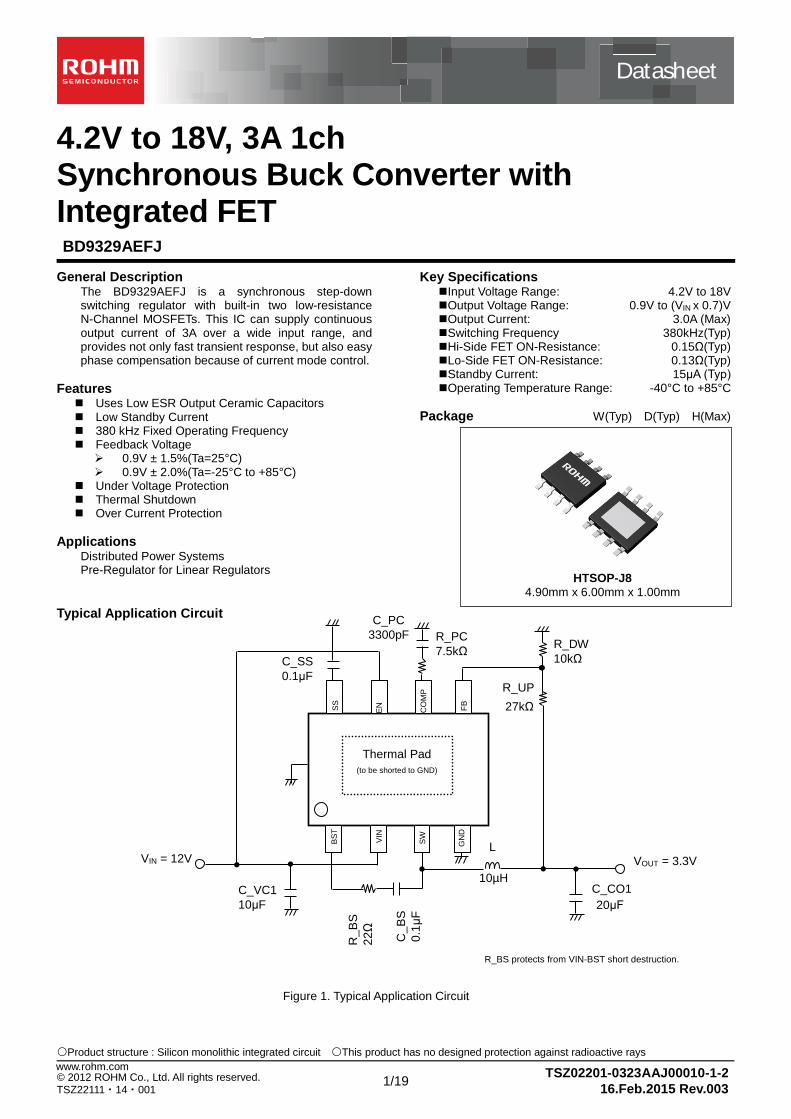
Datasheet © 2012 ROHM Co., Ltd. All rights reserved. www.rohm.com TSZ22111・14・001 TSZ02201-0323AAJ00010-1-2 16.Feb.2015 Rev.003 4.2V to 18V, 3A 1ch Synchronous Buck Converter with Integrated FET BD9329AEFJ General Description The BD9329AEFJ is a synchronous step-down switching regulator with built-in two low-resistance N-Channel MOSFETs. This IC can supply continuous output current of 3A over a wide input range, and provides not only fast transient response, but also easy phase compensation because of current mode control. Features Uses Low ESR Output Ceramic Capacitors Low Standby Current 380 kHz Fixed Operating Frequency Feedback Voltage 0.9V ± 1.5%(Ta=25°C) 0.9V ± 2.0%(Ta=-25°C to +85°C) Under Voltage Protection Thermal Shutdown Over Current Protection Applications Distributed Power Systems Pre-Regulator for Linear Regulators Key Specifications Input Voltage Range: 4.2V to 18V Output Voltage Range: 0.9V to (VIN x 0.7)V Output Current: 3.0A (Max) Switching Frequency 380kHz(Typ) Hi-Side FET ON-Resistance: 0.15Ω(Typ) Lo-Side FET ON-Resistance: 0.13Ω(Typ) Standby Current: 15μA (Typ) Operating Temperature Range: -40°C to +85°C Package W(Typ) D(Typ) H(Max) Typical Application Circuit R_BS protects from VIN-BST short destruction. Figure 1. Typical Application Circuit C_CO1 R_PC 7.5kΩ R_UP C_BS 0.1μF 10μH C_VC1 10μF C_PC 3300pF R_DW 10kΩ 27kΩ 20μF C_SS 0.1μF L SS EN COMP FB BST VIN GND SW Thermal Pad (to be shorted to GND) VIN = 12V VOUT = 3.3V R_BS 22Ω HTSOP-J8 4.90mm x 6.00mm x 1.00mm 〇Product structure : Silicon monolithic integrated circuit 〇This product has no designed protection against radioactive rays 1/19
Transcript of BD9329AEFJ : Power...
Datasheet
© 2012 ROHM Co., Ltd. All rights reserved. www.rohm.com
TSZ22111・14・001 TSZ02201-0323AAJ00010-1-2
16.Feb.2015 Rev.003
4.2V to 18V, 3A 1ch Synchronous Buck Converter with Integrated FET BD9329AEFJ
General Description
The BD9329AEFJ is a synchronous step-down switching regulator with built-in two low-resistance N-Channel MOSFETs. This IC can supply continuous output current of 3A over a wide input range, and provides not only fast transient response, but also easy phase compensation because of current mode control.
Features Uses Low ESR Output Ceramic Capacitors Low Standby Current 380 kHz Fixed Operating Frequency Feedback Voltage 0.9V ± 1.5%(Ta=25°C) 0.9V ± 2.0%(Ta=-25°C to +85°C)
Under Voltage Protection Thermal Shutdown Over Current Protection
Applications Distributed Power Systems Pre-Regulator for Linear Regulators
Key Specifications Input Voltage Range: 4.2V to 18V Output Voltage Range: 0.9V to (VIN x 0.7)V Output Current: 3.0A (Max) Switching Frequency 380kHz(Typ) Hi-Side FET ON-Resistance: 0.15Ω(Typ) Lo-Side FET ON-Resistance: 0.13Ω(Typ) Standby Current: 15μA (Typ) Operating Temperature Range: -40°C to +85°C
Package W(Typ) D(Typ) H(Max)
Typical Application Circuit
R_BS protects from VIN-BST short destruction.
Figure 1. Typical Application Circuit
C_CO1
R_PC 7.5kΩ
R_UP
C_B
S
0.1μ
F
10µH C_VC1 10μF
C_PC 3300pF
R_DW 10kΩ
27kΩ
20μF
C_SS 0.1μF
L
SS
EN
CO
MP
FB
BST
VIN
GN
D
SW
Thermal Pad (to be shorted to GND)
VIN = 12V VOUT = 3.3V
R_B
S
22Ω
HTSOP-J8 4.90mm x 6.00mm x 1.00mm
〇Product structure : Silicon monolithic integrated circuit 〇This product has no designed protection against radioactive rays
1/19
BD9329AEFJ
© 2012 ROHM Co., Ltd. All rights reserved. www.rohm.com
TSZ22111・15・001 TSZ02201-0323AAJ00010-1-2
16.Feb.2015 Rev.003
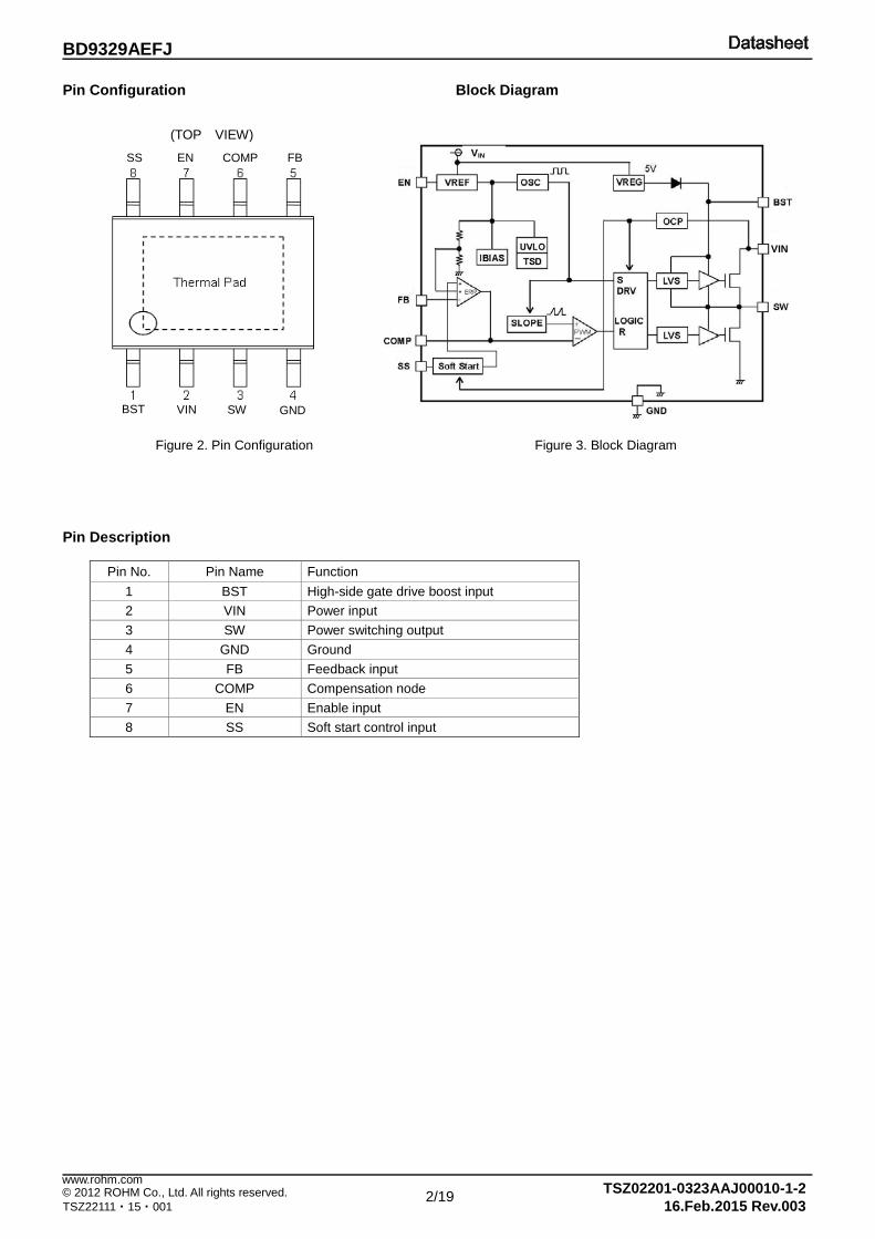
Pin Configuration Block Diagram
Figure 2. Pin Configuration Figure 3. Block Diagram
Pin Description
Pin No. Pin Name Function 1 BST High-side gate drive boost input 2 VIN Power input 3 SW Power switching output 4 GND Ground 5 FB Feedback input 6 COMP Compensation node 7 EN Enable input 8 SS Soft start control input
(TOP VIEW)
BST VIN SW GND
FB COMP EN SS
VIN
VIN
2/19
BD9329AEFJ
© 2012 ROHM Co., Ltd. All rights reserved. www.rohm.com
TSZ22111・15・001 TSZ02201-0323AAJ00010-1-2
16.Feb.2015 Rev.003
Absolute Maximum Ratings (Ta = 25°C)
Parameter Symbol Rating Unit
Supply Voltage VIN 20 V Switch Voltage VSW 20 V Power Dissipation for HTSOP-J8 Pd 3.76 (Note 1) W Package Thermal Resistance θja (Note 2) θja 29.27 °C/W Package Thermal Resistance θjc (Note 2) θjc 3.75 °C/W Operating Temperature Range Topr -40 to +85 °C Storage Temperature Range Tstg -55 to +150 °C Maximum Junction Temperature Tjmax 150 °C BST Voltage VBST VSW+7 V EN Voltage VEN 20 V All Other Pins VOTH 20 V
(Note 1) Reduced by 30.08 mW/°C over 25°C (Mount on 4-layer 70.0mm x 70.0mm x 1.6mm board) (Note 2) Mount on 4-layer 50mm x 30mm x 1.6mm application board Caution: Operating the IC over the absolute maximum ratings may damage the IC. The damage can either be a short circuit between pins or an open circuit between pins and the internal circuitry. Therefore, it is important to consider circuit protection measures, such as adding a fuse, in case the IC is operated over the absolute maximum ratings.
Recommended Operating Conditions (Ta= -40°C to +85°C)
Parameter Symbol Rating
Unit Min Typ Max
Supply Voltage VIN 4.2 12 18 V SW Voltage VSW -0.5 - +18 V Output Current ISW3 - - 3 A Output Voltage Range VRANGE 0.9 - VIN x 0.7 V
Electrical Characteristics (Unless otherwise specified VIN=12V Ta=25°C)
Parameter Symbol Limit
Unit Conditions Min Typ Max
Error Amplifier Block FB Input Bias Current IFB - 0.02 2 µA Feedback Voltage1 VFB1 0.886 0.900 0.914 V Voltage Follower Feedback Voltage2 VFB2 0.882 0.900 0.918 V Ta=-25°C to +85°C SW Block – SW Hi-Side FET ON-Resistance RONH - 0.15 - Ω ISW= -0.8A Lo-Side FET ON-Resistance RONL - 0.13 - Ω ISW= 0.8A
Hi/Lo-Side FET Leak Current ILEAKN - 0 10 µA VIN= 18V, VSW = 0V / 18V
Switch Current Limit ILIMIT3 3.5 - - A Maximum Duty Cycle MDUTY - 90 - % VFB= 0V General Enable Sink Current IEN 90 180 270 µA VEN= 12V Enable Threshold Voltage VEN 1.0 1.2 1.4 V Under Voltage Lockout Threshold VUVLO 3.5 3.75 4.0 V VIN Rising Under Voltage Lockout Hysteresis VHYS - 0.3 - V Soft Start Current ISS 5 10 15 µA VSS= 0V Soft Start Time tSS - 22 - ms CSS= 0.1 µF Operating Frequency fOSC 300 380 460 kHz Circuit Current ICC - 1.2 3 mA VFB= 1.5V, VEN= 12V Standby Current IQUI - 15 27 µA VEN= 0V
3/19
BD9329AEFJ
© 2012 ROHM Co., Ltd. All rights reserved. www.rohm.com
TSZ22111・15・001 TSZ02201-0323AAJ00010-1-2
16.Feb.2015 Rev.003
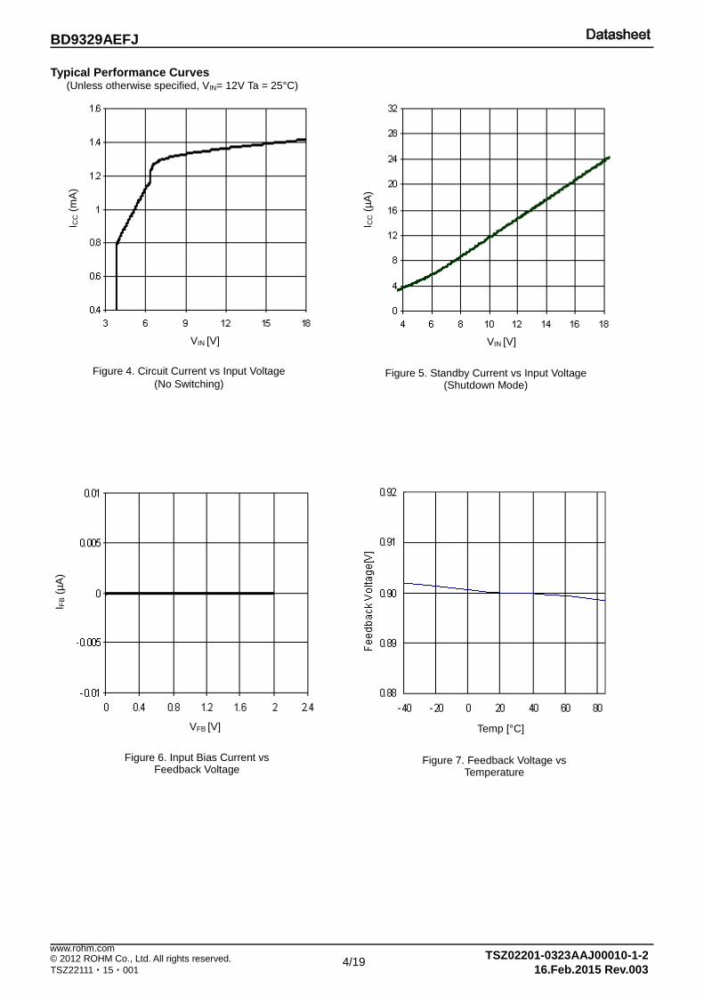
Typical Performance Curves (Unless otherwise specified, VIN= 12V Ta = 25°C)
Figure 7. Feedback Voltage vs
Temperature
Figure 4. Circuit Current vs Input Voltage
(No Switching)
Figure 5. Standby Current vs Input Voltage
(Shutdown Mode)
Figure 6. Input Bias Current vs
Feedback Voltage
I CC (m
A)
VIN [V]
I CC (µ
A)
VIN [V]
I FB
(µA
)
VFB [V] Temp [°C]
4/19
BD9329AEFJ
© 2012 ROHM Co., Ltd. All rights reserved. www.rohm.com
TSZ22111・15・001 TSZ02201-0323AAJ00010-1-2
16.Feb.2015 Rev.003
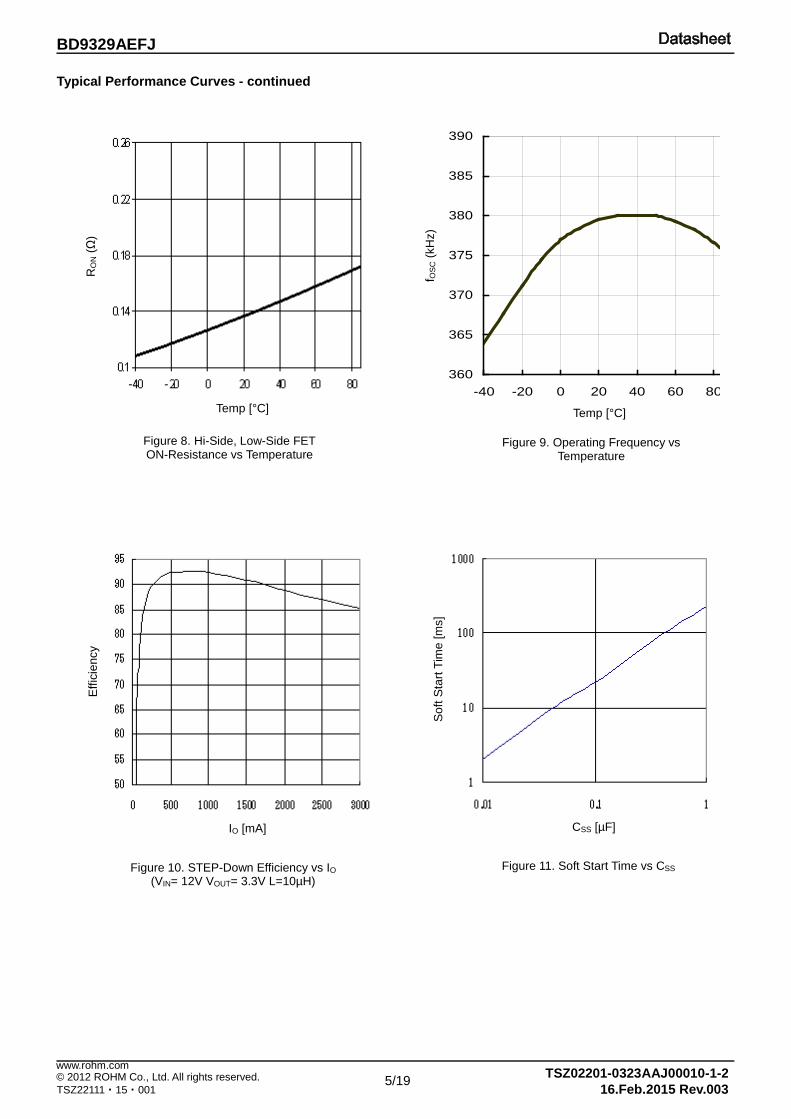
Typical Performance Curves - continued
Figure 8. Hi-Side, Low-Side FET ON-Resistance vs Temperature
Figure 9. Operating Frequency vs
Temperature
Figure 10. STEP-Down Efficiency vs IO
(VIN= 12V VOUT= 3.3V L=10µH)
Figure 11. Soft Start Time vs CSS
RO
N (Ω
)
Temp [°C]
360
365
370
375
380
385
390
-40 -20 0 20 40 60 80
TEMP (°C)
FOSC
(kHz
)f O
SC (k
Hz)
Temp [°C]
Effi
cien
cy
IO [mA]
Sof
t Sta
rt Ti
me
[ms]
CSS [µF]
5/19
BD9329AEFJ
© 2012 ROHM Co., Ltd. All rights reserved. www.rohm.com
TSZ22111・15・001 TSZ02201-0323AAJ00010-1-2
16.Feb.2015 Rev.003
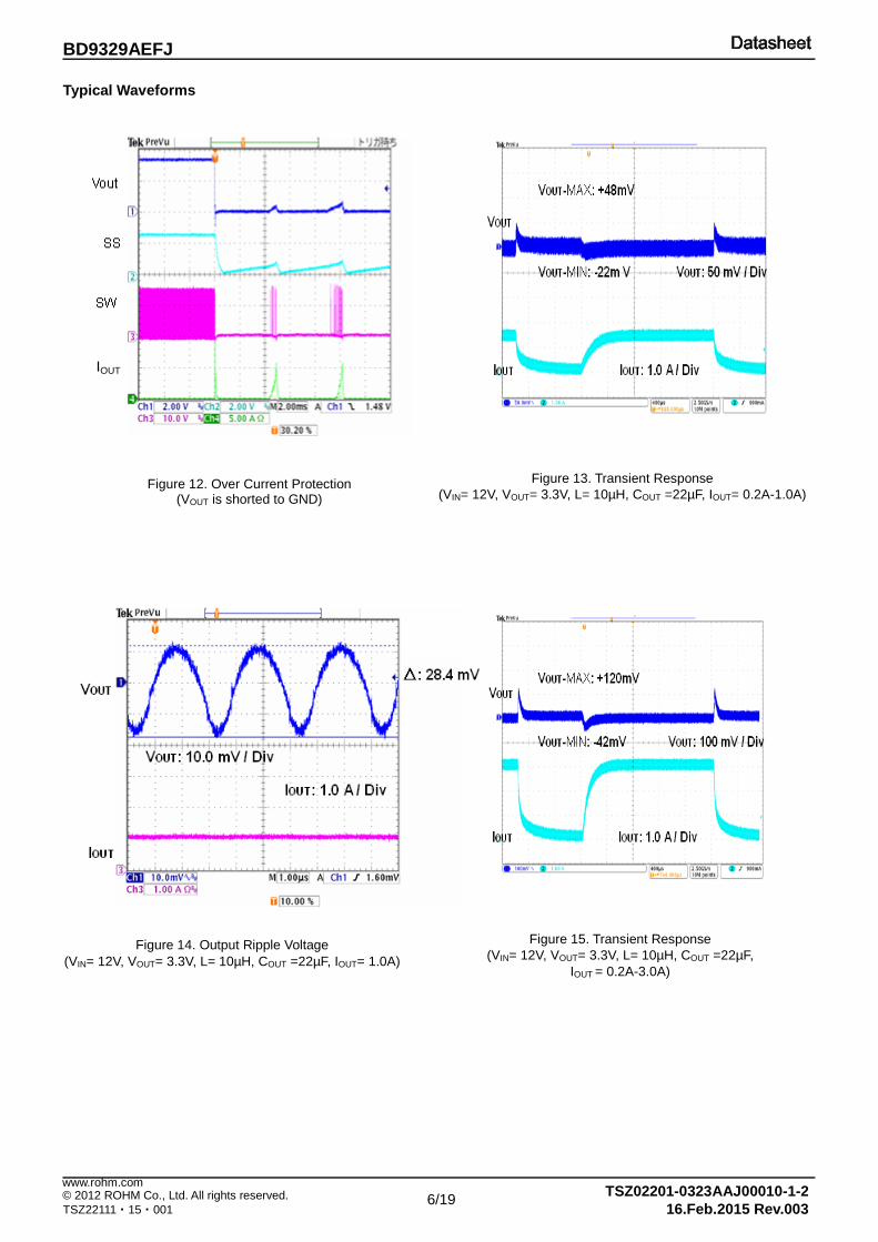
Typical Waveforms
Figure 12. Over Current Protection
(VOUT is shorted to GND)
Figure 13. Transient Response
(VIN= 12V, VOUT= 3.3V, L= 10µH, COUT =22µF, IOUT= 0.2A-1.0A)
Figure 15. Transient Response
(VIN= 12V, VOUT= 3.3V, L= 10µH, COUT =22µF, IOUT = 0.2A-3.0A)
Figure 14. Output Ripple Voltage
(VIN= 12V, VOUT= 3.3V, L= 10µH, COUT =22µF, IOUT= 1.0A)
IOUT
6/19
BD9329AEFJ
© 2012 ROHM Co., Ltd. All rights reserved. www.rohm.com
TSZ22111・15・001 TSZ02201-0323AAJ00010-1-2
16.Feb.2015 Rev.003
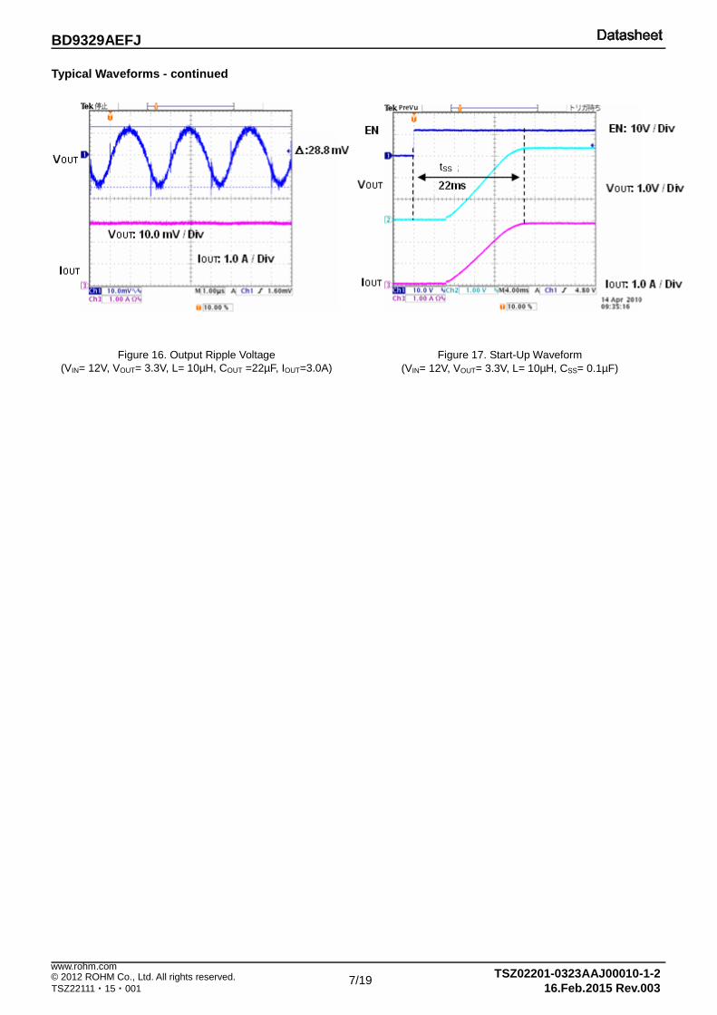
Typical Waveforms - continued
Figure 17. Start-Up Waveform
(VIN= 12V, VOUT= 3.3V, L= 10µH, CSS= 0.1µF)
Figure 16. Output Ripple Voltage
(VIN= 12V, VOUT= 3.3V, L= 10µH, COUT =22µF, IOUT=3.0A)
tSS
7/19
BD9329AEFJ
© 2012 ROHM Co., Ltd. All rights reserved. www.rohm.com
TSZ22111・15・001 TSZ02201-0323AAJ00010-1-2
16.Feb.2015 Rev.003
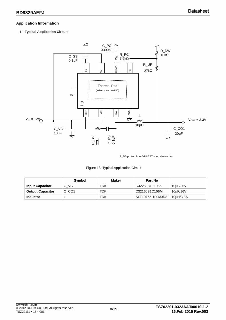
Application Information
1. Typical Application Circuit R_BS protect from VIN-BST short destruction.
Figure 18. Typical Application Circuit
Symbol Maker Part No Input Capacitor C_VC1 TDK C3225JB1E106K 10µF/25V Output Capacitor C_CO1 TDK C3216JB1C106M 10µF/16V Inductor L TDK SLF10165-100M3R8 10µH/3.8A
C_B
S
0.1μ
F
VOUT = 3.3V
R_B
S
22Ω
VIN = 12V
C_CO1
R_UP
10µH C_VC1 10μF
C_PC 3300pF R_DW
10kΩ
27kΩ
20μF
C_SS 0.1μF
L
SS
EN
CO
MP-
FB
BST
VIN
GN
D
SW
Thermal Pad (to be shorted to GND)
R_PC 7.5kΩ
8/19
BD9329AEFJ
© 2012 ROHM Co., Ltd. All rights reserved. www.rohm.com
TSZ22111・15・001 TSZ02201-0323AAJ00010-1-2
16.Feb.2015 Rev.003
2. Block Operation
(1) VREG This block generates a constant voltage for DC/DC boosting.
(2) VREF
This block generates an internal reference voltage of 5.1V (Typ).
(3) TSD/UVLO TSD (Thermal shutdown)/UVLO (Under Voltage Lockout) protection block. The TSD circuit shuts down the IC at high temperature. The UVLO circuit shuts down the IC when the VIN voltage is low.
(4) Error Amp Block (ERR)
This block compares the reference voltage and the feedback voltage from the output. The output voltage of this block, which is connected to COMP pin, determines the switching duty cycle. At the time of startup, since the soft-start is operated by the SS pin voltage, the COMP pin voltage is limited to the SS pin voltage.
(5) Oscillator Block (OSC) This block generates the oscillating frequency.
(6) SLOPE Block
This block generates the triangular waveform with the use of the clock created by OSC. The generated triangular waveform is sent to the PWM comparator.
(7) PWM Block
The COMP pin voltage output of the error amp is compared with the SLOPE block's triangular waveform to determine the switching duty. Since the switching duty cycle is limited by the maximum duty ratio which is determined internally, 100% duty cycle cannot be achieved.
(8) DRV Block
This is the A DC/DC driver block that accepts signal from the PWM block to drive the power FETs.
(9) OCP Block OCP (Over Current Protection) block. The current that flows through the FETs is detected, and OCP starts when it reaches 3.5A (min). After OCP detection, switching is turned OFF and the SS capacitor is discharged. OCP is self-recovery type (not latch).
(10) Soft-Start Circuit
This circuit prevents output voltage overshoot or inrush current by making the output voltage rise gradually while restricting the current at the time of startup.
9/19
BD9329AEFJ
© 2012 ROHM Co., Ltd. All rights reserved. www.rohm.com
TSZ22111・15・001 TSZ02201-0323AAJ00010-1-2
16.Feb.2015 Rev.003
3. Selecting Application Components
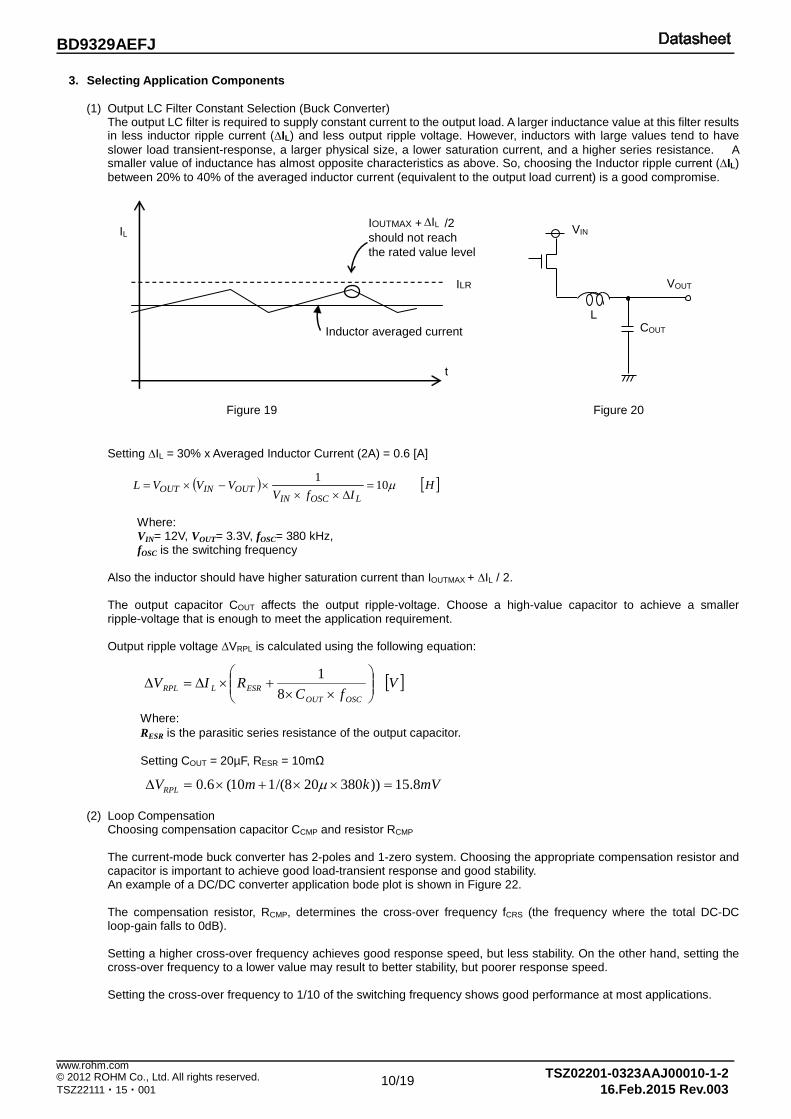
(1) Output LC Filter Constant Selection (Buck Converter) The output LC filter is required to supply constant current to the output load. A larger inductance value at this filter results in less inductor ripple current (∆IL) and less output ripple voltage. However, inductors with large values tend to have slower load transient-response, a larger physical size, a lower saturation current, and a higher series resistance. A smaller value of inductance has almost opposite characteristics as above. So, choosing the Inductor ripple current (∆IL) between 20% to 40% of the averaged inductor current (equivalent to the output load current) is a good compromise.
Figure 19 Figure 20
Setting ∆IL = 30% x Averaged Inductor Current (2A) = 0.6 [A] Where:
VIN= 12V, VOUT= 3.3V, fOSC= 380 kHz, fOSC is the switching frequency Also the inductor should have higher saturation current than IOUTMAX + ∆IL / 2. The output capacitor COUT affects the output ripple-voltage. Choose a high-value capacitor to achieve a smaller ripple-voltage that is enough to meet the application requirement. Output ripple voltage ∆VRPL is calculated using the following equation:
Where: RESR is the parasitic series resistance of the output capacitor. Setting COUT = 20µF, RESR = 10mΩ
(2) Loop Compensation
Choosing compensation capacitor CCMP and resistor RCMP The current-mode buck converter has 2-poles and 1-zero system. Choosing the appropriate compensation resistor and capacitor is important to achieve good load-transient response and good stability. An example of a DC/DC converter application bode plot is shown in Figure 22. The compensation resistor, RCMP, determines the cross-over frequency fCRS (the frequency where the total DC-DC loop-gain falls to 0dB). Setting a higher cross-over frequency achieves good response speed, but less stability. On the other hand, setting the cross-over frequency to a lower value may result to better stability, but poorer response speed. Setting the cross-over frequency to 1/10 of the switching frequency shows good performance at most applications.
IL
t
IOUTMAX + ∆IL /2 should not reach the rated value level
ILR
Inductor averaged current
VOUT
L
VIN
COUT
( ) [ ]HIfV
VVVLLOSCIN
OUTINOUT µ101=
∆×××−×=
[ ]VfC
RIVOSCOUT
ESRLRPL
××
+×∆=∆8
1
∆IL IL
mVkmVRPL 8.15))380208/(110(6.0 =××+×=∆ µ
10/19
BD9329AEFJ
© 2012 ROHM Co., Ltd. All rights reserved. www.rohm.com
TSZ22111・15・001 TSZ02201-0323AAJ00010-1-2
16.Feb.2015 Rev.003
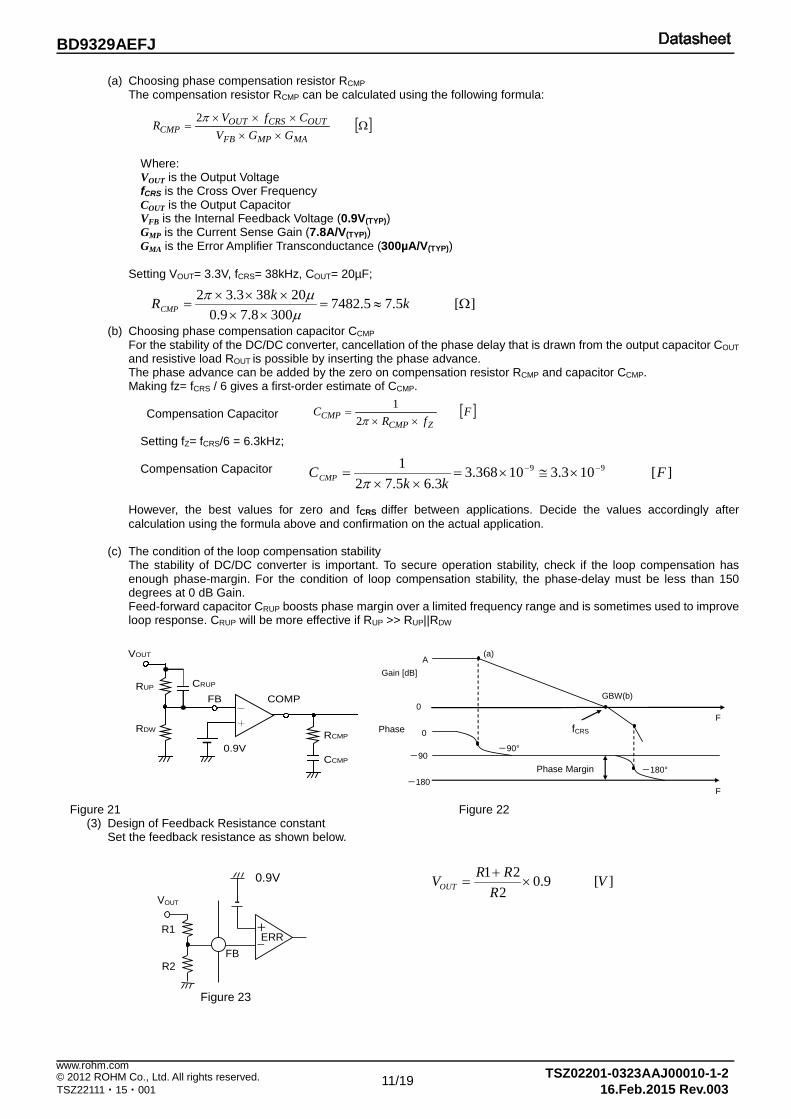
(a) Choosing phase compensation resistor RCMP The compensation resistor RCMP can be calculated using the following formula:
Where: VOUT is the Output Voltage fCRS is the Cross Over Frequency COUT is the Output Capacitor VFB is the Internal Feedback Voltage (0.9V(TYP)) GMP is the Current Sense Gain (7.8A/V(TYP)) GMA is the Error Amplifier Transconductance (300µA/V(TYP))
Setting VOUT= 3.3V, fCRS= 38kHz, COUT= 20µF;
(b) Choosing phase compensation capacitor CCMP For the stability of the DC/DC converter, cancellation of the phase delay that is drawn from the output capacitor COUT and resistive load ROUT is possible by inserting the phase advance. The phase advance can be added by the zero on compensation resistor RCMP and capacitor CCMP. Making fz= fCRS / 6 gives a first-order estimate of CCMP.
Compensation Capacitor Setting fZ= fCRS/6 = 6.3kHz;
Compensation Capacitor
However, the best values for zero and fCRS differ between applications. Decide the values accordingly after calculation using the formula above and confirmation on the actual application.
(c) The condition of the loop compensation stability The stability of DC/DC converter is important. To secure operation stability, check if the loop compensation has enough phase-margin. For the condition of loop compensation stability, the phase-delay must be less than 150 degrees at 0 dB Gain. Feed-forward capacitor CRUP boosts phase margin over a limited frequency range and is sometimes used to improve loop response. CRUP will be more effective if RUP >> RUP||RDW
Figure 21 Figure 22
(3) Design of Feedback Resistance constant Set the feedback resistance as shown below.
Figure 23
-
+
VOUT
RUP
CCMP
COMP
RCMP
FB
RDW
0.9V
CRUP
+
-
VOUT
R1
R2
ERR
0.9V
FB
[ ]Ω××
×××=
MAMPFB
OUTCRSOUTCMP GGV
CfVR
π2
[ ]FfR
CZCMP
CMP ××=
π21
][9.02
21 VR
RRVOUT ×+
=
PHASE MARGIN -180°
-90°
-180
-90
0
0
A (a)
GBW(b)
F
F
Gain [dB]
PHASE FCRS
Phase Margin
Phase fCRS
][5.75.74823008.79.0
20383.32Ω≈=
×××××
= kkRCMP µµπ
][103.310368.33.65.72
1 99 Fkk
CCMP−− ×≅×=
××=
π
11/19
BD9329AEFJ
© 2012 ROHM Co., Ltd. All rights reserved. www.rohm.com
TSZ22111・15・001 TSZ02201-0323AAJ00010-1-2
16.Feb.2015 Rev.003
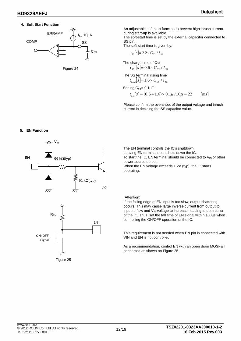
4. Soft Start Function An adjustable soft-start function to prevent high inrush current during start-up is available. The soft-start time is set by the external capacitor connected to SS pin. The soft-start time is given by; The charge time of CSS
The SS terminal rising time
Setting CSS= 0.1µF
Please confirm the overshoot of the output voltage and inrush current in deciding the SS capacitor value.
5. EN Function
The EN terminal controls the IC’s shutdown. Leaving EN terminal open shuts down the IC. To start the IC, EN terminal should be connected to VIN or other power source output. When the EN voltage exceeds 1.2V (typ), the IC starts operating. (Attention) If the falling edge of EN input is too slow, output chattering occurs. This may cause large inverse current from output to input to flow and VIN voltage to increase, leading to destruction of the IC. Thus, set the fall time of EN signal within 100µs when controlling the ON/OFF operation of the IC. This requirement is not needed when EN pin is connected with VIN and EN is not controlled. As a recommendation, control EN with an open drain MOSFET connected as shown on Figure 25.
Figure 25
VIN
EN
66 kΩ(typ)
91 kΩ(typ)
CSS
SS + + -
COMP
ISS 10µA ERRAMP
↓ ↓
Figure 24
[ ] SSSSSS ICst /2.2 ×=
REN
ON/OFFSignal
EN
REN
[ ] SSSSSS ICst /6.01 ×=
[ ] SSSSSS ICst /6.12 ×=
][2210/1.0)6.16.0(][ msstSS =×+= µµ
12/19
BD9329AEFJ
© 2012 ROHM Co., Ltd. All rights reserved. www.rohm.com
TSZ22111・15・001 TSZ02201-0323AAJ00010-1-2
16.Feb.2015 Rev.003
CIN FET COUT
L VOUT
VIN
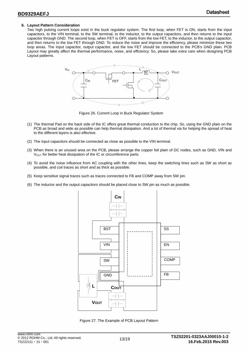
6. Layout Pattern Consideration Two high pulsing current loops exist in the buck regulator system. The first loop, when FET is ON, starts from the input capacitors, to the VIN terminal, to the SW terminal, to the inductor, to the output capacitors, and then returns to the input capacitor through GND. The second loop, when FET is OFF, starts from the low FET, to the inductor, to the output capacitor, and then returns to the low FET through GND. To reduce the noise and improve the efficiency, please minimize these two loop areas. The input capacitor, output capacitor, and the low FET should be connected to the PCB’s GND plain. PCB Layout may greatly affect the thermal performance, noise, and efficiency. So, please take extra care when designing PCB Layout patterns.
(1) The thermal Pad on the back side of the IC offers great thermal conduction to the chip. So, using the GND plain on the PCB as broad and wide as possible can help thermal dissipation. And a lot of thermal via for helping the spread of heat to the different layers is also effective.
(2) The input capacitors should be connected as close as possible to the VIN terminal. (3) When there is an unused area on the PCB, please arrange the copper foil plain of DC nodes, such as GND, VIN and
VOUT for better heat dissipation of the IC or circumference parts. (4) To avoid the noise influence from AC coupling with the other lines, keep the switching lines such as SW as short as
possible, and coil traces as short and as thick as possible. (5) Keep sensitive signal traces such as traces connected to FB and COMP away from SW pin. (6) The inductor and the output capacitors should be placed close to SW pin as much as possible.
Figure 26. Current Loop in Buck Regulator System
Figure 27. The Example of PCB Layout Pattern
COMP
BST
VIN
SW
FB
SS
EN
GND
COUT L
VOUT
CIN
13/19
BD9329AEFJ
© 2012 ROHM Co., Ltd. All rights reserved. www.rohm.com
TSZ22111・15・001 TSZ02201-0323AAJ00010-1-2
16.Feb.2015 Rev.003
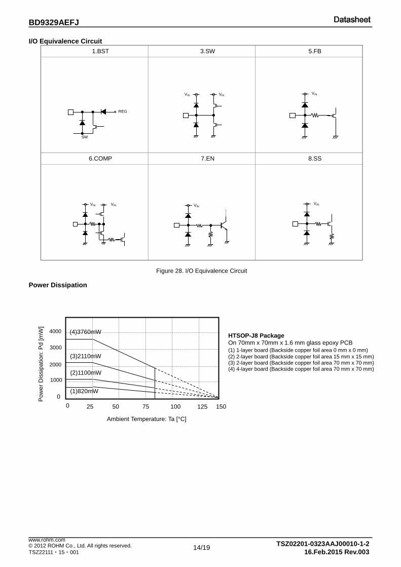
I/O Equivalence Circuit 1.BST 3.SW 5.FB
6.COMP 7.EN 8.SS
Figure 28. I/O Equivalence Circuit
Power Dissipation
VIN VIN
SW
REG
VIN
VIN
VIN VIN
VIN
150
0 50 75 100 125
2000
4000
1000
3000
25
Pow
er D
issi
patio
n: P
d [m
W]
Ambient Temperature: Ta [°C]
(1)820mW
(2)1100mW
(3)2110mW
(4)3760mW
0
HTSOP-J8 Package On 70mm x 70mm x 1.6 mm glass epoxy PCB (1) 1-layer board (Backside copper foil area 0 mm x 0 mm) (2) 2-layer board (Backside copper foil area 15 mm x 15 mm) (3) 2-layer board (Backside copper foil area 70 mm x 70 mm) (4) 4-layer board (Backside copper foil area 70 mm x 70 mm)
14/19
BD9329AEFJ
© 2012 ROHM Co., Ltd. All rights reserved. www.rohm.com
TSZ22111・15・001 TSZ02201-0323AAJ00010-1-2
16.Feb.2015 Rev.003
Operational Notes
1. Reverse Connection of Power Supply Connecting the power supply in reverse polarity can damage the IC. Take precautions against reverse polarity when connecting the power supply, such as mounting an external diode between the power supply and the IC’s power supply pins.
2. Power Supply Lines Design the PCB layout pattern to provide low impedance supply lines. Separate the ground and supply lines of the digital and analog blocks to prevent noise in the ground and supply lines of the digital block from affecting the analog block. Furthermore, connect a capacitor to ground at all power supply pins. Consider the effect of temperature and aging on the capacitance value when using electrolytic capacitors.
3. Ground Voltage Ensure that no pins are at a voltage below that of the ground pin at any time, even during transient condition.
4. Ground Wiring Pattern
When using both small-signal and large-current ground traces, the two ground traces should be routed separately but connected to a single ground at the reference point of the application board to avoid fluctuations in the small-signal ground caused by large currents. Also ensure that the ground traces of external components do not cause variations on the ground voltage. The ground lines must be as short and thick as possible to reduce line impedance.
5. Thermal Consideration
Should by any chance the power dissipation rating be exceeded the rise in temperature of the chip may result in deterioration of the properties of the chip. The absolute maximum rating of the Pd stated in this specification is when the IC is mounted on a 70mm x 70mm x 1.6mm glass epoxy board. In case of exceeding this absolute maximum rating, increase the board size and copper area to prevent exceeding the Pd rating.
6. Recommended Operating Conditions
These conditions represent a range within which the expected characteristics of the IC can be approximately obtained. The electrical characteristics are guaranteed under the conditions of each parameter.
7. Inrush Current
When power is first supplied to the IC, it is possible that the internal logic may be unstable and inrush current may flow instantaneously due to the internal powering sequence and delays, especially if the IC has more than one power supply. Therefore, give special consideration to power coupling capacitance, power wiring, width of ground wiring, and routing of connections.
8. Operation Under Strong Electromagnetic Field
Operating the IC in the presence of a strong electromagnetic field may cause the IC to malfunction.
9. Testing on Application Boards When testing the IC on an application board, connecting a capacitor directly to a low-impedance output pin may subject the IC to stress. Always discharge capacitors completely after each process or step. The IC’s power supply should always be turned off completely before connecting or removing it from the test setup during the inspection process. To prevent damage from static discharge, ground the IC during assembly and use similar precautions during transport and storage.
10. Inter-pin Short and Mounting Errors Ensure that the direction and position are correct when mounting the IC on the PCB. Incorrect mounting may result in damaging the IC. Avoid nearby pins being shorted to each other especially to ground, power supply and output pin. Inter-pin shorts could be due to many reasons such as metal particles, water droplets (in very humid environment) and unintentional solder bridge deposited in between pins during assembly to name a few.
15/19
BD9329AEFJ
© 2012 ROHM Co., Ltd. All rights reserved. www.rohm.com
TSZ22111・15・001 TSZ02201-0323AAJ00010-1-2
16.Feb.2015 Rev.003
Operational Notes – continued
11. Unused Input Pins Input pins of an IC are often connected to the gate of a MOS transistor. The gate has extremely high impedance and extremely low capacitance. If left unconnected, the electric field from the outside can easily charge it. The small charge acquired in this way is enough to produce a significant effect on the conduction through the transistor and cause unexpected operation of the IC. So unless otherwise specified, unused input pins should be connected to the power supply or ground line.
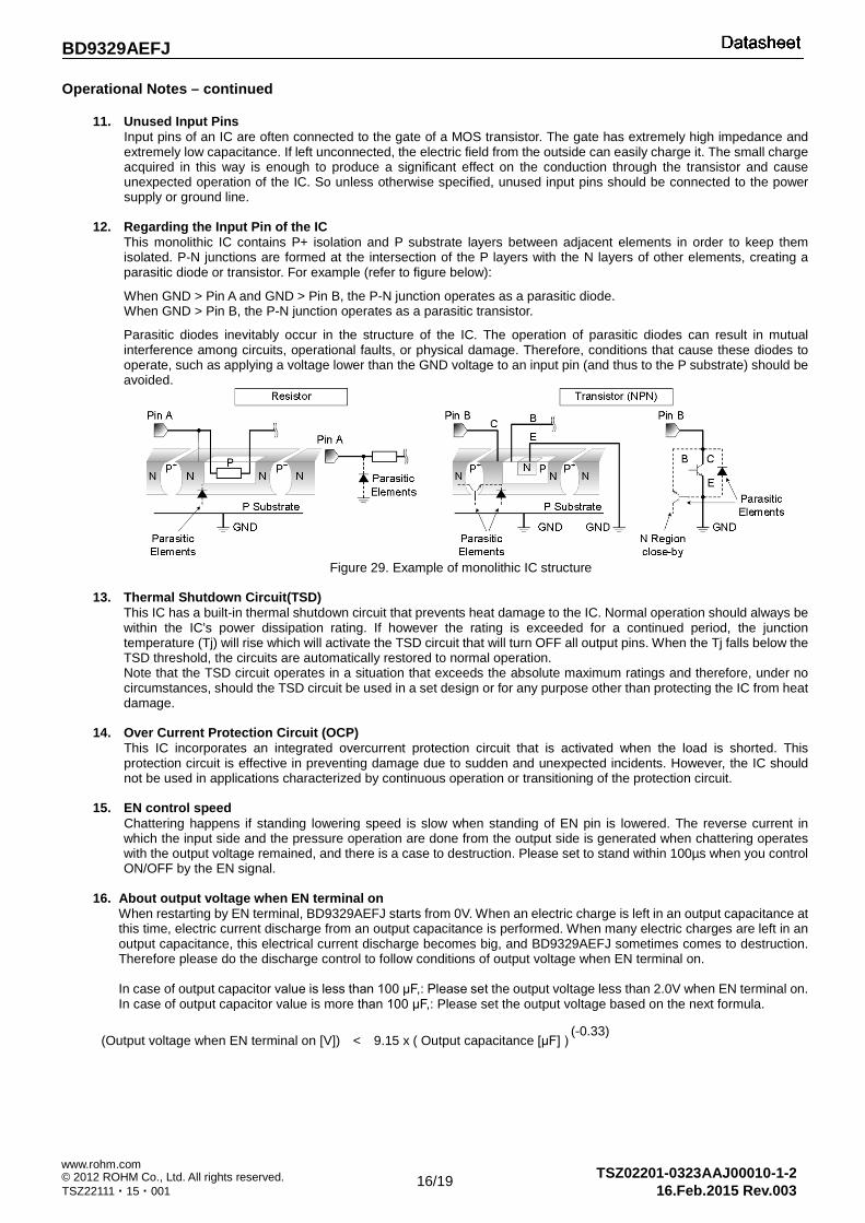
12. Regarding the Input Pin of the IC
This monolithic IC contains P+ isolation and P substrate layers between adjacent elements in order to keep them isolated. P-N junctions are formed at the intersection of the P layers with the N layers of other elements, creating a parasitic diode or transistor. For example (refer to figure below):
When GND > Pin A and GND > Pin B, the P-N junction operates as a parasitic diode. When GND > Pin B, the P-N junction operates as a parasitic transistor.
Parasitic diodes inevitably occur in the structure of the IC. The operation of parasitic diodes can result in mutual interference among circuits, operational faults, or physical damage. Therefore, conditions that cause these diodes to operate, such as applying a voltage lower than the GND voltage to an input pin (and thus to the P substrate) should be avoided.
Figure 29. Example of monolithic IC structure
13. Thermal Shutdown Circuit(TSD) This IC has a built-in thermal shutdown circuit that prevents heat damage to the IC. Normal operation should always be within the IC’s power dissipation rating. If however the rating is exceeded for a continued period, the junction temperature (Tj) will rise which will activate the TSD circuit that will turn OFF all output pins. When the Tj falls below the TSD threshold, the circuits are automatically restored to normal operation. Note that the TSD circuit operates in a situation that exceeds the absolute maximum ratings and therefore, under no circumstances, should the TSD circuit be used in a set design or for any purpose other than protecting the IC from heat damage.
14. Over Current Protection Circuit (OCP)
This IC incorporates an integrated overcurrent protection circuit that is activated when the load is shorted. This protection circuit is effective in preventing damage due to sudden and unexpected incidents. However, the IC should not be used in applications characterized by continuous operation or transitioning of the protection circuit.
15. EN control speed
Chattering happens if standing lowering speed is slow when standing of EN pin is lowered. The reverse current in which the input side and the pressure operation are done from the output side is generated when chattering operates with the output voltage remained, and there is a case to destruction. Please set to stand within 100µs when you control ON/OFF by the EN signal.
16. About output voltage when EN terminal on
When restarting by EN terminal, BD9329AEFJ starts from 0V. When an electric charge is left in an output capacitance at this time, electric current discharge from an output capacitance is performed. When many electric charges are left in an output capacitance, this electrical current discharge becomes big, and BD9329AEFJ sometimes comes to destruction. Therefore please do the discharge control to follow conditions of output voltage when EN terminal on.
In case of output capacitor value is less than 100 μF,: Please set the output voltage less than 2.0V when EN terminal on. In case of output capacitor value is more than 100 μF,: Please set the output voltage based on the next formula.
(Output voltage when EN terminal on [V]) < 9.15 x ( Output capacitance [μF] ) (-0.33)
16/19
BD9329AEFJ
© 2012 ROHM Co., Ltd. All rights reserved. www.rohm.com
TSZ22111・15・001 TSZ02201-0323AAJ00010-1-2
16.Feb.2015 Rev.003
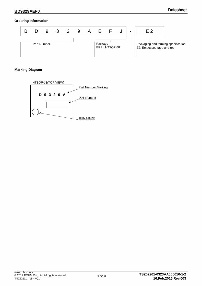
Ordering Information
B D 9 3 2 9 A E F J - E 2 Part Number
Package EFJ : HTSOP-J8
Packaging and forming specification E2: Embossed tape and reel
Marking Diagram
HTSOP-J8(TOP VIEW)
D 9 3 2 9 A
Part Number Marking
LOT Number
1PIN MARK
17/19
BD9329AEFJ
© 2012 ROHM Co., Ltd. All rights reserved. www.rohm.com
TSZ22111・15・001 TSZ02201-0323AAJ00010-1-2
16.Feb.2015 Rev.003
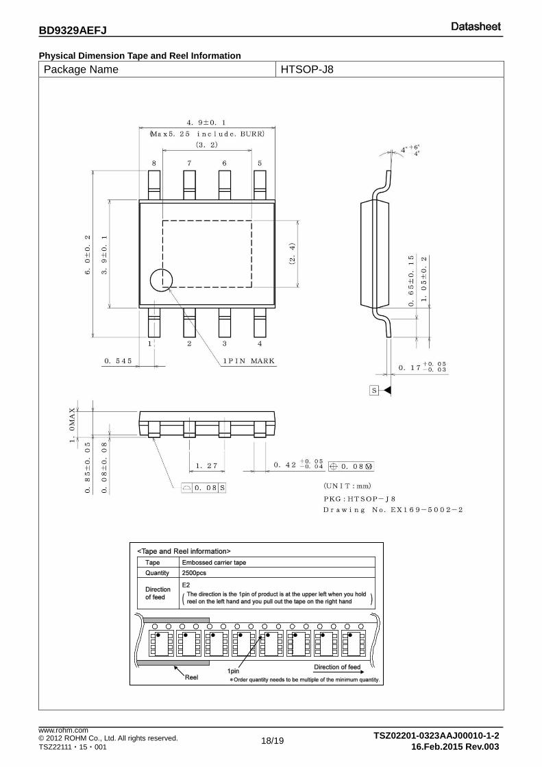
Physical Dimension Tape and Reel Information Package Name HTSOP-J8
18/19
BD9329AEFJ
© 2012 ROHM Co., Ltd. All rights reserved. www.rohm.com
TSZ22111・15・001 TSZ02201-0323AAJ00010-1-2
16.Feb.2015 Rev.003
Revision History
Date Revision Changes
11.Apr.2012 001 New Release 03.Sep.2014 002 Applied the ROHM Standard Style and improved understandability. 16.Feb.2015 003 Add “16.about output voltage when EN terminal on” in Operational Notes
19/19
DatasheetDatasheet
Notice-GE Rev.004© 2013 ROHM Co., Ltd. All rights reserved.
Notice Precaution on using ROHM Products
1. Our Products are designed and manufactured for application in ordinary electronic equipments (such as AV equipment, OA equipment, telecommunication equipment, home electronic appliances, amusement equipment, etc.). If you intend to use our Products in devices requiring extremely high reliability (such as medical equipment (Note 1), transport equipment, traffic equipment, aircraft/spacecraft, nuclear power controllers, fuel controllers, car equipment including car accessories, safety devices, etc.) and whose malfunction or failure may cause loss of human life, bodily injury or serious damage to property (“Specific Applications”), please consult with the ROHM sales representative in advance. Unless otherwise agreed in writing by ROHM in advance, ROHM shall not be in any way responsible or liable for any damages, expenses or losses incurred by you or third parties arising from the use of any ROHM’s Products for Specific Applications.
(Note1) Medical Equipment Classification of the Specific Applications JAPAN USA EU CHINA
CLASSⅢ CLASSⅢ
CLASSⅡb CLASSⅢ
CLASSⅣ CLASSⅢ
2. ROHM designs and manufactures its Products subject to strict quality control system. However, semiconductor products can fail or malfunction at a certain rate. Please be sure to implement, at your own responsibilities, adequate safety measures including but not limited to fail-safe design against the physical injury, damage to any property, which a failure or malfunction of our Products may cause. The following are examples of safety measures:
[a] Installation of protection circuits or other protective devices to improve system safety [b] Installation of redundant circuits to reduce the impact of single or multiple circuit failure
3. Our Products are designed and manufactured for use under standard conditions and not under any special or extraordinary environments or conditions, as exemplified below. Accordingly, ROHM shall not be in any way responsible or liable for any damages, expenses or losses arising from the use of any ROHM’s Products under any special or extraordinary environments or conditions. If you intend to use our Products under any special or extraordinary environments or conditions (as exemplified below), your independent verification and confirmation of product performance, reliability, etc, prior to use, must be necessary:
[a] Use of our Products in any types of liquid, including water, oils, chemicals, and organic solvents [b] Use of our Products outdoors or in places where the Products are exposed to direct sunlight or dust [c] Use of our Products in places where the Products are exposed to sea wind or corrosive gases, including Cl2,
H2S, NH3, SO2, and NO2 [d] Use of our Products in places where the Products are exposed to static electricity or electromagnetic waves [e] Use of our Products in proximity to heat-producing components, plastic cords, or other flammable items [f] Sealing or coating our Products with resin or other coating materials [g] Use of our Products without cleaning residue of flux (even if you use no-clean type fluxes, cleaning residue of
flux is recommended); or Washing our Products by using water or water-soluble cleaning agents for cleaning residue after soldering
[h] Use of the Products in places subject to dew condensation
4. The Products are not subject to radiation-proof design. 5. Please verify and confirm characteristics of the final or mounted products in using the Products. 6. In particular, if a transient load (a large amount of load applied in a short period of time, such as pulse. is applied,
confirmation of performance characteristics after on-board mounting is strongly recommended. Avoid applying power exceeding normal rated power; exceeding the power rating under steady-state loading condition may negatively affect product performance and reliability.
7. De-rate Power Dissipation (Pd) depending on Ambient temperature (Ta). When used in sealed area, confirm the actual
ambient temperature. 8. Confirm that operation temperature is within the specified range described in the product specification. 9. ROHM shall not be in any way responsible or liable for failure induced under deviant condition from what is defined in
this document.
Precaution for Mounting / Circuit board design 1. When a highly active halogenous (chlorine, bromine, etc.) flux is used, the residue of flux may negatively affect product
performance and reliability.
2. In principle, the reflow soldering method must be used on a surface-mount products, the flow soldering method must be used on a through hole mount products. If the flow soldering method is preferred on a surface-mount products, please consult with the ROHM representative in advance.
For details, please refer to ROHM Mounting specification

DatasheetDatasheet
Notice-GE Rev.004© 2013 ROHM Co., Ltd. All rights reserved.
Precautions Regarding Application Examples and External Circuits 1. If change is made to the constant of an external circuit, please allow a sufficient margin considering variations of the
characteristics of the Products and external components, including transient characteristics, as well as static characteristics.
2. You agree that application notes, reference designs, and associated data and information contained in this document
are presented only as guidance for Products use. Therefore, in case you use such information, you are solely responsible for it and you must exercise your own independent verification and judgment in the use of such information contained in this document. ROHM shall not be in any way responsible or liable for any damages, expenses or losses incurred by you or third parties arising from the use of such information.
Precaution for Electrostatic
This Product is electrostatic sensitive product, which may be damaged due to electrostatic discharge. Please take proper caution in your manufacturing process and storage so that voltage exceeding the Products maximum rating will not be applied to Products. Please take special care under dry condition (e.g. Grounding of human body / equipment / solder iron, isolation from charged objects, setting of Ionizer, friction prevention and temperature / humidity control).
Precaution for Storage / Transportation 1. Product performance and soldered connections may deteriorate if the Products are stored in the places where:
[a] the Products are exposed to sea winds or corrosive gases, including Cl2, H2S, NH3, SO2, and NO2 [b] the temperature or humidity exceeds those recommended by ROHM [c] the Products are exposed to direct sunshine or condensation [d] the Products are exposed to high Electrostatic
2. Even under ROHM recommended storage condition, solderability of products out of recommended storage time period may be degraded. It is strongly recommended to confirm solderability before using Products of which storage time is exceeding the recommended storage time period.
3. Store / transport cartons in the correct direction, which is indicated on a carton with a symbol. Otherwise bent leads
may occur due to excessive stress applied when dropping of a carton. 4. Use Products within the specified time after opening a humidity barrier bag. Baking is required before using Products of
which storage time is exceeding the recommended storage time period.
Precaution for Product Label QR code printed on ROHM Products label is for ROHM’s internal use only.
Precaution for Disposition When disposing Products please dispose them properly using an authorized industry waste company.
Precaution for Foreign Exchange and Foreign Trade act Since our Products might fall under controlled goods prescribed by the applicable foreign exchange and foreign trade act, please consult with ROHM representative in case of export.
Precaution Regarding Intellectual Property Rights 1. All information and data including but not limited to application example contained in this document is for reference
only. ROHM does not warrant that foregoing information or data will not infringe any intellectual property rights or any other rights of any third party regarding such information or data. ROHM shall not be in any way responsible or liable for infringement of any intellectual property rights or other damages arising from use of such information or data.:
2. No license, expressly or implied, is granted hereby under any intellectual property rights or other rights of ROHM or any
third parties with respect to the information contained in this document.
Other Precaution 1. This document may not be reprinted or reproduced, in whole or in part, without prior written consent of ROHM. 2. The Products may not be disassembled, converted, modified, reproduced or otherwise changed without prior written
consent of ROHM. 3. In no event shall you use in any way whatsoever the Products and the related technical information contained in the
Products or this document for any military purposes, including but not limited to, the development of mass-destruction weapons.
4. The proper names of companies or products described in this document are trademarks or registered trademarks of
ROHM, its affiliated companies or third parties.

DatasheetDatasheet
Notice – WE Rev.001© 2015 ROHM Co., Ltd. All rights reserved.
General Precaution 1. Before you use our Pro ducts, you are requested to care fully read this document and fully understand its contents.
ROHM shall n ot be in an y way responsible or liabl e for fa ilure, malfunction or acci dent arising from the use of a ny ROHM’s Products against warning, caution or note contained in this document.
2. All information contained in this docume nt is current as of the issuing date and subj ect to change without any prior
notice. Before purchasing or using ROHM’s Products, please confirm the la test information with a ROHM sale s representative.
3. The information contained in this doc ument is provi ded on an “as is” basis and ROHM does not warrant that all
information contained in this document is accurate an d/or error-free. ROHM shall not be in an y way responsible or liable for any damages, expenses or losses incurred by you or third parties resulting from inaccuracy or errors of or concerning such information.