PGND PGND CTL2 SYNC Secondary power supply series for...
41
〇Product structure : Silicon monolithic integrated circuit 〇This product has no designed protection against radioactive rays . 1/38 TSZ02201-0J2J0AL01130-1-2 © 2016 ROHM Co., Ltd. All rights reserved. 24.Feb.2017 Rev.002 TSZ22111 • 14 • 001 www.rohm.com Secondary power supply series for automotive 2.6V to 5.5V, 2A, 0.3MHz to 2.4MHz Synchronous Step-Down Converter BD90521MUV-C / BD90521EFV-C General Description The BD90521MUV/EFV -C is a synchronous step-down converter which operates in current mode. It can operate with maximum frequency of 2.4 MHz, and can downsize external parts such as inductor. It can supply a maximum output current of 2A with built-in Pch and Nch output MOSFET. Output voltage and oscillation frequency can be adjusted by external resistors and can also be synchronized with an external clock. Features AEC-Q100 Qualified (Note 1) Up to 2.4MHz movement Excellent Load Response by Current Mode Control Built-in Pch/Nch Output MOSFET. Frequency Synchronization with External Clock. Output Error Monitor Terminal (PGOOD Terminal) Adjustable Output Voltage and Oscillation Frequency by External Resistors. Built-in Self-Reset Type Overcurrent Protection. Built-in Output Overvoltage/Short Circuit Detection. Built-in Temperature Protection (TSD) and UVLO. (Note 1: Grade 1) Applications Automotive Battery-Powered Supplies (Cluster Panels, Car Multimedia) Industrial / Consumer Supplies Other electronic equipment Key Specifications Operating Temperature Range(Ta): -40°C to +125°C Input Voltage Range: 2.6V to 5.5V Output Current: 2.0A(Max) Reference Voltage Accuracy: ±1.5 % Output Voltage Range: 0.6V to 5.0V Switching Frequency: 0.3MHz to 2.4MHz Package W(Typ) x D(Typ) x H(Max) VQFN20SV4040 4.00mm x 4.00mm x 1.00mm HTSSOP-B20 6.50mm x 6.40mm x 1.00mm Typical Application Circuit SW SW N.C PVIN PVIN SEL RT N.C FB SS COMP GND CTL1 EN VIN SYNC CTL2 PGOOD PGND PGND L1 R2 C3 R3 Vo R5 R1 R6 Co R IN C IN 1 C IN 2 C1 V IN VIN or EN VQFN20SV4040 HTSSOP-B20 Datasheet
Transcript of PGND PGND CTL2 SYNC Secondary power supply series for...

〇Product structure : Silicon monolithic integrated circuit 〇This product has no designed protection against radioactive rays
.
1/38
TSZ02201-0J2J0AL01130-1-2 © 2016 ROHM Co., Ltd. All rights reserved. 24.Feb.2017 Rev.002 TSZ22111 • 14 • 001
www.rohm.com
Secondary power supply series for automotive
2.6V to 5.5V, 2A, 0.3MHz to 2.4MHz Synchronous Step-Down Converter BD90521MUV-C / BD90521EFV-C
General Description The BD90521MUV/EFV -C is a synchronous step-down converter which operates in current mode. It can operate with maximum frequency of 2.4 MHz, and can downsize external parts such as inductor. It can supply a maximum output current of 2A with built-in Pch and Nch output MOSFET. Output voltage and oscillation frequency can be adjusted by external resistors and can also be synchronized with an external clock.
Features AEC-Q100 Qualified (Note 1) Up to 2.4MHz movement Excellent Load Response by Current Mode Control Built-in Pch/Nch Output MOSFET. Frequency Synchronization with External Clock. Output Error Monitor Terminal (PGOOD Terminal) Adjustable Output Voltage and Oscillation Frequency
by External Resistors. Built-in Self-Reset Type Overcurrent Protection. Built-in Output Overvoltage/Short Circuit Detection. Built-in Temperature Protection (TSD) and UVLO. (Note 1: Grade 1)
Applications Automotive Battery-Powered Supplies
(Cluster Panels, Car Multimedia) Industrial / Consumer Supplies Other electronic equipment
Key Specifications Operating Temperature Range(Ta): -40°C to +125°C Input Voltage Range: 2.6V to 5.5V Output Current: 2.0A(Max) Reference Voltage Accuracy: ±1.5 % Output Voltage Range: 0.6V to 5.0V Switching Frequency: 0.3MHz to 2.4MHz
Package W(Typ) x D(Typ) x H(Max) VQFN20SV4040 4.00mm x 4.00mm x 1.00mm HTSSOP-B20 6.50mm x 6.40mm x 1.00mm
Typical Application Circuit
SW
SW
N.C
PVIN
PVIN
SEL
RT
N.C
FB
SS
CO
MP
GN
D
CTL1
EN
VIN
SYN
C
CTL2
PG
OO
D
PG
ND
PG
ND
L1
R2C3
R3Vo
R5
R1 R6
CoRIN CIN1
CIN2
C1
VIN
VINorEN
VQFN20SV4040 HTSSOP-B20
Datasheet
2/38
TSZ02201-0J2J0AL01130-1-2 24.Feb.2017 Rev.002
BD90521MUV-C / BD90521EFV-C
© 2016 ROHM Co., Ltd. All rights reserved. www.rohm.com
TSZ22111 • 15 • 001
Contents
General Description ........................................................................................................................................................................ 1
Features.......................................................................................................................................................................................... 1
Applications .................................................................................................................................................................................... 1
Key Specifications .......................................................................................................................................................................... 1
Package ...................................................................................................................................................................1
Typical Application Circuit ............................................................................................................................................................... 1
Contents ......................................................................................................................................................................................... 2
Pin Configurations .......................................................................................................................................................................... 3
Pin Descriptions .............................................................................................................................................................................. 3
Block Diagram ................................................................................................................................................................................ 4
Description of Blocks ...................................................................................................................................................................... 4
Absolute Maximum Ratings ............................................................................................................................................................ 6
Thermal Resistance ........................................................................................................................................................................ 6
Recommended Operating Conditions ............................................................................................................................................. 7
Electrical Characteristics................................................................................................................................................................. 8
Typical Performance Curves ........................................................................................................................................................... 9
Description of Operation and Timing Chart ................................................................................................................................... 14
Selection of Components Externally Connected ........................................................................................................................... 17
Recommended Parts Manufacturer List ....................................................................................................................................... 23
Application Examples 1 ................................................................................................................................................................ 24
Application Examples 2 ................................................................................................................................................................ 26
Notes on the PCB Layout ............................................................................................................................................................. 28
Power Dissipation ......................................................................................................................................................................... 31
I/O Equivalent Circuits .................................................................................................................................................................. 32
Operational Notes ......................................................................................................................................................................... 33
Ordering Information ..................................................................................................................................................................... 35
Marking Diagrams ......................................................................................................................................................................... 35
Physical Dimension, Tape and Reel Information ........................................................................................................................... 36
Physical Dimension, Tape and Reel Information ........................................................................................................................... 37
Revision History ............................................................................................................................................................................ 38

3/38
TSZ02201-0J2J0AL01130-1-2 24.Feb.2017 Rev.002
BD90521MUV-C / BD90521EFV-C
© 2016 ROHM Co., Ltd. All rights reserved. www.rohm.com
TSZ22111 • 15 • 001
Pin Configurations
Pin Descriptions
E-Pad is a back radiation pad. Excellent radiation property is obtainable by connection to internal PCB ground-plane using multiple via. Use CTL1 terminal by applying 2.1 V or higher when enable is on. Use CTL2 terminal by short-circuiting to GND. If N.C pin is shorted to GND, heat radiation performance becomes higher.
Pin No. Symbol Function Pin No. Symbol Function
1 (3) SW SW pin 11 (13) SS Soft start time setting pin
2 (4) SW SW pin 12 (14) FB Output feedback pin
3 (5) N.C - 13 (15) N.C -
4 (6) PVIN Power supply pin for output FET 14 (16) RT Operating frequency setting pin
5 (7) PVIN Power supply pin for output FET 15 (17) SEL RT setting frequency/ Synchronization select pin
6 (8) VIN Power supply pin 16 (18) SYNC External clock input pin
7 (9) EN Enable pin 17 (19) CTL2 Test pin
8 (10) CTL1 Test pin 18 (20) PGOOD Power good output pin
9 (11) GND GND pin 19 (1) PGND GND pin for output FET
10 (12) COMP Error amp output pin 20 (2) PGND GND pin for output FET
1
2
3
4
5
6
7
8
9
10
15
14
13
12
11
20
19
18
17
16
SW
SW
N.C
PVIN
PVIN
SEL
RT
N.C
FB
SS
PGND
PGND PGOOD
CTL2
SYNC
VIN
EN
CTL1
COMP
GND
(TOP VIEW)
E-Pad
VQFN20SV4040 HTSSOP-B20
1
2
3
4
5
6 7 8 9 10
15
14
13
12
11
20 19 18 17 16
SEL
RT
N.C
PVIN
PVIN
SW
SW
N.C
FB
SS
PG
ND
PG
ND
PG
OO
D
CT
L2
SY
NC
VIN EN
GN
D
CO
MP
CT
L1
E-Pad
(TOP VIEW)

4/38
TSZ02201-0J2J0AL01130-1-2 24.Feb.2017 Rev.002
BD90521MUV-C / BD90521EFV-C
© 2016 ROHM Co., Ltd. All rights reserved. www.rohm.com
TSZ22111 • 15 • 001
Block Diagram
Description of Blocks
・ERROR AMPLIFER
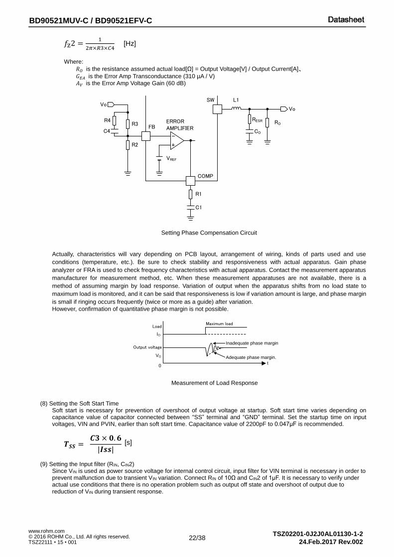
This is an error amplifier using reference voltage of 0.6V (Typ) and “FB” terminal voltage as input. (Refer to p. 21 to p. 22 for phase compensation setting method). Duty width of switching pulse is controlled with “COMP” of error amplifier output. Output voltage is set using “FB” terminal. Phase compensation can be adjusted by connecting capacitor and resistor to “COMP” terminal.
・SOFT START
This is a function for preventing overshoot of output voltage by gradually raising non-inverting input voltage of ERROR AMPLIFIER to gradually increase duty of switching pulse at power on. Soft start can be set by connecting a capacitor between “GND” terminals with “SS terminal”. (Refer to p. 22.)
・OSCILLATOR
Oscillation frequency of 0.3 MHz to 2.4 MHz can be set by connecting a resistor between “RT” terminal and “GND” terminal in the circuit which generates pulse waveform to be input to SLOPE. (Refer to Figure 18 on p. 21)OSCILLATOR output sends clock signal to DRV. OSCILLATOR output is also used as the clock of SCP counter.
・SLOPE
This is the block for generating saw-tooth wave from the clock formed by OSCILLATOR. Generated saw-tooth wave is combined with feedback current of coil current and sent to PWM COMPARATOR.
・PWM COMPARATOR
This is a comparator that compares SLOPE output and ERROR AMPLIFIER output.
・DRV This is a latch circuit having OSCILLATOR output (set) and PWM COMPARATOR output (reset) as input. It generates PWM control signal and outputs gate signal for FET drive.
UVLO/TSD
SCP/OVP
R
DRV
S
SLOPE
OSCILLATOR
VOLTAGE
REFERENCEUVLO
SOFT
START
ERROR
AMPLIFER
0.6VPWM
COMPARATOR
0.54V
0.66V
OVP
SCP
PGOOD
FB
SS
EN
VIN COMP
PVIN
PVIN
SW
SW
PGND
PGND
CTL1SYNCRTGND SEL
CTL2
+
-
+OCP Vth

5/38
TSZ02201-0J2J0AL01130-1-2 24.Feb.2017 Rev.002
BD90521MUV-C / BD90521EFV-C
© 2016 ROHM Co., Ltd. All rights reserved. www.rohm.com
TSZ22111 • 15 • 001
・TSD (Thermal Shut Down)
This is an overheat protection circuit. In order to prevent IC thermal destruction/runaway, output is turned off when chip temperature rises to about 150°C or higher. It is recovered when temperature returns to constant temperature. However, since overheat protection circuit is essentially built-in for the purpose of protection of IC itself, carry out thermal design to keep chip temperature below about 150°C as TSD detection temperature.
・OCP VTH(Over Current Protection)
This is an overcurrent protection circuit. When output Pch POWER MOS FET is turned on and voltage between drain and source exceeds internal reference voltage value, overcurrent protection activates. This overcurrent protection is self-reset type. When overcurrent protection activates, duty becomes small and output voltage is reduced. However, since these protection circuits are effective in protection from destruction due to sudden accidents, avoid using them when continuous protection circuit is in action.
・SCP (Short Current Protection)
This is a load short-circuit protection circuit. When the state of output of 60% or lower is detected in oscillation cycle × 256 (s), POWER MOS FET is turned off. If output voltage is recovered to 60% or higher before completion of 256 cycles, POWER MOS FET is not turned off. This load short-circuit protection is cancelled after retention of oscillation cycle × 2048 (s), and it is restarted with soft start. Elongation of off time results in decrease of mean output current. During startup of power source, this function is masked until output reaches set voltage to prevent startup failure.
・UVLO (Under Voltage Lock-Out)
This is a low voltage wrong operation prevention circuit. It prevents wrong operation of internal circuits during power source voltage startup and when power source voltage is reduced. Power source voltage is monitored and when it is reduced to 2.25 V (Typ) or lower, output POWER MOS FET is turned off. When UVLO is cancelled, it is restarted with soft start. This threshold has hysteresis of 100 mV (Typ).
・VOLTAGE REFERENCE
It supplies reference voltage to internal circuits.
・OVP
When output voltage is detected to have exceeded set value + 10%, Pch FET and Nch FET of output is turned off. After detection, when output is reduced and the overvoltage state is cancelled, switching action is restarted. There is hysteresis of 2% in overvoltage detection voltage and cancel voltage.
・PGOOD
When output voltage is below 90% or above 110% of set value, output error state is assumed, and PGOOD terminal is turned “Low”. There is hysteresis of 2% in detection voltage and cancel voltage. At the time of EN OFF and when UVLO and TSD are in action, PGOOD terminal output is also turned “Low”. If VIN input voltage exceeds 2 V, PGOOD output becomes effective. Since output is open drain type, connect pull up to VIN or an external power source with resistance of 10kΩ - 100 kΩ.

6/38
TSZ02201-0J2J0AL01130-1-2 24.Feb.2017 Rev.002
BD90521MUV-C / BD90521EFV-C
© 2016 ROHM Co., Ltd. All rights reserved. www.rohm.com
TSZ22111 • 15 • 001
Absolute Maximum Ratings (Ta = 25°C)
Parameter Symbol Rating Unit
Supply Voltage VIN, PVIN -0.3 to 7 V
EN Pin Voltage (Note 1) VEN -0.3 to 5.9 V
SYNC Pin Voltage VSYNC -0.3 to VIN V
SEL Pin Voltage VSEL -0.3 to 7 V
FB Pin Voltage VFB -0.3 to VIN V
COMP Pin Voltage VCOMP -0.3 to VIN V
SS Pin Voltage VSS -0.3 to VIN V
RT Pin Voltage VRT -0.3 to VIN V
PGOOD Pin Voltage VPGOOD -0.3 to 7 V
Maximum Junction Temperature Tjmax +150 °C
Storage Temperature Range Tstg -55 to +150 °C
ESD Rating (HBM) VESD, HBM ±2000 V
(Note 1) State enters test mode when EN terminal exceeds 6 V.
Caution: Operating the IC over the absolute maximum ratings may damage the IC. The damage can either be a short circuit between pins or an open circuit
between pins and the internal circuitry. Therefore, it is important to consider circuit protection measures, such as adding a fuse, in case the IC is operated over
the absolute maximum ratings.
Thermal Resistance(Note 1)
項目 Symbol Thermal Resistance (Typ)
Unit 1s(Note 3) 2s2p(Note 4)
VQFN20SV4040
Junction to Ambient θJA 153.9 37.4 °C / W
Junction to Top Characterization Parameter(Note 2) ΨJT 13 7 °C / W
HTSSOP-B20
Junction to Ambient θJA 143.0 26.8 °C / W
Junction to Top Characterization Parameter(Note 2) ΨJT 8 4 °C / W
(Note 1) Based on JESD51-2A(Still-Air) (Note 2) The thermal characterization parameter to report the difference between junction temperature and the temperature at the top center of the outside surface
of the component package. (Note 3) Using a PCB board based on JESD51-3.
Layer Number of Measurement Board
Material Board Size
Single FR-4 114.3mm x 76.2mm x 1.57mmt
Top
Copper Pattern Thickness
Footprints and Traces 70μm
(Note 4) Using a PCB board based on JESD51-5,7.
Layer Number of Measurement Board
Material Board Size Thermal Via (Note 5)
Pitch Diameter
4 Layers FR-4 114.3mm x 76.2mm x 1.6mmt 1.20mm Φ0.30mm
Top 2 Internal Layers Bottom
Copper Pattern Thickness Copper Pattern Thickness Copper Pattern Thickness
Footprints and Traces 70μm 74.2mm x 74.2mm 35μm 74.2mm x 74.2mm 70μm
(Note 5) This thermal via connects with the copper pattern of all layers.
7/38
TSZ02201-0J2J0AL01130-1-2 24.Feb.2017 Rev.002
BD90521MUV-C / BD90521EFV-C
© 2016 ROHM Co., Ltd. All rights reserved. www.rohm.com
TSZ22111 • 15 • 001
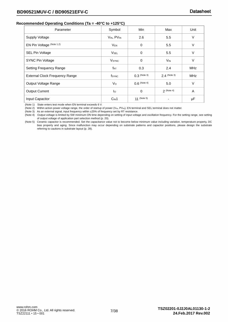
Recommended Operating Conditions (Ta = -40°C to +125°C)
Parameter Symbol Min Max Unit
Supply Voltage VIN, PVIN 2.6 5.5 V
EN Pin Voltage (Note 1,2) VEN 0 5.5 V
SEL Pin Voltage VSEL 0 5.5 V
SYNC Pin Voltage VSYNC 0 VIN V
Setting Frequency Range fRT 0.3 2.4 MHz
External Clock Frequency Range fSYNC 0.3 (Note 3) 2.4 (Note 3) MHz
Output Voltage Range VO 0.6 (Note 4) 5.0 V
Output Current IO 0 2 (Note 4) A
Input Capacitor CIN1 11 (Note 5) - μF
(Note 1) State enters test mode when EN terminal exceeds 6 V.
(Note 2) Within action power voltage range, the order of startup of power (VIN, PVIN), EN terminal and SEL terminal does not matter.
(Note 3) As an external signal, input frequency within ±25% of frequency set by RT resistance.
(Note 4) Output voltage is limited by SW minimum ON time depending on setting of input voltage and oscillation frequency. For the setting range, see setting
of output voltage of application part selection method (p. 20).
(Note 5) Ceramic capacitor is recommended. Set the capacitance value not to become below minimum value including variation, temperature property, DC
bias property and aging. Since malfunction may occur depending on substrate patterns and capacitor positions, please design the substrate
referring to cautions in substrate layout (p. 28).

8/38
TSZ02201-0J2J0AL01130-1-2 24.Feb.2017 Rev.002
BD90521MUV-C / BD90521EFV-C
© 2016 ROHM Co., Ltd. All rights reserved. www.rohm.com
TSZ22111 • 15 • 001
Electrical Characteristics
(Unless otherwise specified, -40 °C ≤ Ta ≤ +125 °C、VIN = PVIN = 5 V、VEN = 3.3 V、VCTL1 = 5 V)
Parameter Symbol Limit
Unit Conditions Min Typ Max
Standby Circuit Current ISDN - 0 1 μA VEN = 0V, Ta = 25°C
Circuit Current IIN - 700 1050 μA VFB = 0.63V, Ta = 25°C
EN ON Voltage VEN_ON 2.1 - - V
EN OFF Voltage VEN_OFF - - 0.7 V
EN Input Current IEN 3 7 14 μA VEN = 3.3V
UVLO ON Voltage VUVLO_ON - 2.25 2.40 V Sweep Down
UVLO OFF Voltage VUVLO_OFF - 2.35 2.50 V Sweep Up
FB Input Current IFB - 0 0.5 μA VFB = 0.6V
Reference Voltage VREF 0.591 0.600 0.609 V FB = COMP
COMP Source Current ICOMP_SOURCE -40 -20 -5 μA
COMP Sink Current ICOMP_SINK 5 20 40 μA
SS Charge Current ISS -3 -2 -1 μA VSS = 0.6V
SS Discharge Current RSS 100 200 300 Ω VSS = 0.6V
Operating Frequency fOSC 0.85 1.00 1.15 MHz R6 = 240kΩ
SW Min ON Time 1 tSW_ON1 - 100 - ns IO = 0A
SW Min ON Time 2 tSW_ON2 - 80 - ns IO = 1A
SW Min OFF Time tSW_OFF - 100 - ns
SW ON-Resistance H RON_SW_H - 90 180 mΩ ISW = -50mA, VFB = 0.58V
SW ON-Resistance L RON_SW_L - 60 120 mΩ ISW = +50mA, VFB = 0.62V
Over-Current Detect
Current ISW_OCP 2.5 5.5 - A
SYNC ON Voltage VSYNC_ON 0.8 x VIN - - V
SYNC OFF Voltage VSYNC_OFF - - 0.2 x VIN V
SYNC Input Current ISYNC 4 10 20 μA VSYNC = 5V
PGOOD Sense FB Voltage VFB_PGOOD1 ±6 ±10 ±14 % Pull up to VIN with 10kΩ
PGOOD ON-Resistance RPGOOD 60 120 240 Ω VPGOOD = 5V
SEL ON Voltage VSEL_ON 2.1 - - V
SEL OFF Voltage VSEL_OFF - - 0.7 V
SEL Input Current ISEL 3 7 14 μA VSEL = 3.3V
9/38
TSZ02201-0J2J0AL01130-1-2 24.Feb.2017 Rev.002
BD90521MUV-C / BD90521EFV-C
© 2016 ROHM Co., Ltd. All rights reserved. www.rohm.com
TSZ22111 • 15 • 001
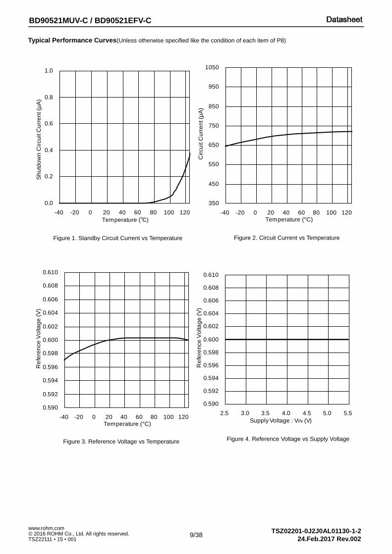
Typical Performance Curves(Unless otherwise specified like the condition of each item of P8)
0.590
0.592
0.594
0.596
0.598
0.600
0.602
0.604
0.606
0.608
0.610
-40 -20 0 20 40 60 80 100 120Temperature (°C)
Re
fere
nce
Vo
lta
ge
(V
)
350
450
550
650
750
850
950
1050
-40 -20 0 20 40 60 80 100 120Temperature (°C)
Cir
cu
it C
urr
en
t (µ
A)
0.0
0.2
0.4
0.6
0.8
1.0
-40 -20 0 20 40 60 80 100 120
Temperature (℃)
Sh
utd
ow
n C
ircu
it C
urr
en
t (µ
A)
Figure 1. Standby Circuit Current vs Temperature Figure 2. Circuit Current vs Temperature
Figure 3. Reference Voltage vs Temperature
Figure 4. Reference Voltage vs Supply Voltage
0.590
0.592
0.594
0.596
0.598
0.600
0.602
0.604
0.606
0.608
0.610
2.5 3.0 3.5 4.0 4.5 5.0 5.5
Supply Voltage : VIN (V)
Re
fere
nce
Vo
lta
ge
(V
)
10/38
TSZ02201-0J2J0AL01130-1-2 24.Feb.2017 Rev.002
BD90521MUV-C / BD90521EFV-C
© 2016 ROHM Co., Ltd. All rights reserved. www.rohm.com
TSZ22111 • 15 • 001
Typical Performance Curves - continued
0.85
0.90
0.95
1.00
1.05
1.10
1.15
-40 -20 0 20 40 60 80 100 120Temperature (°C)
Fre
quency (
MH
z)
0.7
0.9
1.1
1.3
1.5
1.7
1.9
2.1
-40 -20 0 20 40 60 80 100 120Temperature (°C)
EN
ON
/OF
F V
olta
ge
(V
)
2.10
2.15
2.20
2.25
2.30
2.35
2.40
2.45
2.50
-40 -20 0 20 40 60 80 100 120Temperature (°C)
UV
LO
ON
/OF
F V
olta
ge
(V
)
Figure 6. UVLO ON/OFF Voltage vs Temperature
UVLO OFF
UVLO ON
Figure 5. EN ON/OFF Voltage vs Temperature
R6 = 240kΩ
Figure 8. Frequency (1MHz) vs Temperature Figure 7. Frequency vs Supply Voltage
0.80
0.85
0.90
0.95
1.00
1.05
1.10
1.15
1.20
2.5 3.0 3.5 4.0 4.5 5.0 5.5Supply Voltage : VIN (V)
Fre
qu
en
cy (
MH
z)
R6 = 240kΩ

11/38
TSZ02201-0J2J0AL01130-1-2 24.Feb.2017 Rev.002
BD90521MUV-C / BD90521EFV-C
© 2016 ROHM Co., Ltd. All rights reserved. www.rohm.com
TSZ22111 • 15 • 001
Typical Performance Curves - continued
255
270
285
300
315
330
345
-40 -20 0 20 40 60 80 100 120
Temperature (°C)
Fre
qu
en
cy (
kH
z)
2.0
2.2
2.4
2.6
2.8
-40 -20 0 20 40 60 80 100 120Temperature (°C)
Fre
qu
en
cy (
MH
z)
-0.5
-0.4
-0.3
-0.2
-0.1
0.0
0.1
0.2
0.3
0.4
0.5
-40 -20 0 20 40 60 80 100 120Temperature (°C)
FB
In
pu
t C
urr
en
t (µ
A)
R6 = 75kΩ
Figure 9. Frequency (300kHz) vs Temperature
R6 = 910kΩ
Figure 10. Frequency (2.4MHz) vs Temperature
Figure 11. FB Input Current vs Temperature
1.0
1.2
1.4
1.6
1.8
2.0
2.2
2.4
2.6
2.8
3.0
-40 -20 0 20 40 60 80 100 120
Temperature (°C)
SS
Ch
arg
e C
urr
en
t (µ
A)
Figure 12. SS Charge Current vs Temperature

12/38
TSZ02201-0J2J0AL01130-1-2 24.Feb.2017 Rev.002
BD90521MUV-C / BD90521EFV-C
© 2016 ROHM Co., Ltd. All rights reserved. www.rohm.com
TSZ22111 • 15 • 001
Typical Performance Curves - continued
20
40
60
80
100
120
140
-40 -20 0 20 40 60 80 100 120
Temperature (°C)
SW
ON
-Re
sis
tan
ce
(m
Ω)
2.0
2.2
2.4
2.6
2.8
3.0
-40 -20 0 20 40 60 80 100 120
Temperature (°C)
SY
NC
ON
/OF
F V
olta
ge
(V
)
Pch FET
Nch FET
Figure 13. SW ON-Resistance vs Temperature Figure 14. Over-Current Detect Current vs Temperature
Figure 15. SYNC ON/OFF Voltage vs Temperature
-14
-12
-10
-8
-6
-4
-2
0
2
4
6
8
10
12
14
-40 -20 0 20 40 60 80 100 120
Temperature (°C)
PG
OO
D D
ete
ct V
olta
ge
(%
)
PGOOD falling
PGOOD rising
PGOOD rising
PGOOD falling
Figure 16. PGOOD DETECT Voltage vs Temperature
2.5
3.5
4.5
5.5
6.5
7.5
-40 -20 0 20 40 60 80 100 120Temperature (°C)
Ove
r-C
urr
en
t D
ete
ct C
urr
en
t (A
)

13/38
TSZ02201-0J2J0AL01130-1-2 24.Feb.2017 Rev.002
BD90521MUV-C / BD90521EFV-C
© 2016 ROHM Co., Ltd. All rights reserved. www.rohm.com
TSZ22111 • 15 • 001
Typical Performance Curves - continued
60
80
100
120
140
160
180
-40 -20 0 20 40 60 80 100 120
Temperature (°C)
PG
OO
D O
N-R
esis
tan
ce
(Ω
)
Figure 17. PGOOD ON-Resistance vs Temperature

14/38
TSZ02201-0J2J0AL01130-1-2 24.Feb.2017 Rev.002
BD90521MUV-C / BD90521EFV-C
© 2016 ROHM Co., Ltd. All rights reserved. www.rohm.com
TSZ22111 • 15 • 001
Description of Operation and Timing Chart
■ Enable control IC operation is controlled by voltage applied on EN terminal. When Voltage of 2.1 V or higher is applied on EN terminal, output starts in 60 μs(Typ) with soft start. Set the startup time on input voltages, VIN and PVIN, earlier than soft start time. The circuits can be shut down by opening EN terminal or reducing its voltage to below 0.7 V.
■ Protection functions
Since protection circuits are effective in protection from destruction due to sudden accidents, avoid using protection operation continuously.
(1) Short Current Protection (SCP) When the state of output of 60% or lower is detected in oscillation cycle × 256 (s), POWER MOS-FET is turned off. If output voltage has recovered to 60% or higher before completion of 256 cycles, POWER MOS-FET is not turned off. This load short-circuit protection is cancelled after retention for oscillation cycle × 2048 (s), and it is restarted with soft start. Elongation of off time results in decrease of mean output current. During startup of power source, this function is masked until output reaches set voltage to prevent startup failure.
0.6V
SCP detect voltage:
0.36V(Typ)
SCP detect time
LOW
OCP
Threshold
VO
FB
SW
Internal IC
SCP signal
Coil current
Soft Start
SCP Reset
fsw×256cyc
fsw×2048cyc
fsw×256cycSCP detect time
VIN, PVIN
VEN
VSS
VO
VPGOOD
60μs
0.6V
Setting voltage×0.92
Soft start setting time

15/38
TSZ02201-0J2J0AL01130-1-2 24.Feb.2017 Rev.002
BD90521MUV-C / BD90521EFV-C
© 2016 ROHM Co., Ltd. All rights reserved. www.rohm.com
TSZ22111 • 15 • 001
(2) Under Voltage Lock-Out (UVLO) It prevents wrong operation of internal circuits during power source voltage startup and when power source voltage is reduced. Power source voltage is monitored and when it is reduced to 2.25 V (Typ) or lower, output POWER MOS FET is turned off. When UVLO is cancelled, it is restarted with soft start. This threshold has hysteresis of 100 mV (Typ).
(3) Thermal Shut Down (TSD)
In order to prevent IC thermal destruction/runaway, output is turned off when chip temperature rises to about 150°C or higher. It is recovered when temperature returns to constant temperature. However, since overheat protection circuit is essentially built-in for the purpose of protection of IC itself, carry out thermal design to keep chip temperature below about 150°C as TSD detection temperature.
(4) Over Current Protection (OCP) When output Pch POWER MOS FET is turned on and voltage between drain and source exceeds internal reference voltage value, overcurrent protection activates. This overcurrent protection is self-reset type. When overcurrent protection activates, duty becomes small and output voltage is reduced. However, since these protection circuits are effective in protection from destruction due to sudden accidents, avoid using them when continuous protection circuit is in action.
(5) Over Voltage Protection (OVP) When output voltage is detected to have exceeded set value + 10%, Pch FET and Nch FET of output is turned off. After detection, when output is reduced and the overvoltage state is cancelled, switching action is restarted. There is hysteresis of 2% in overvoltage detection voltage and cancel voltage.
VIN
0V
VO
SW
FBSoft Start
hysteresis
UVLO
OFF
Normal operation Normal operationUVLO
UVLO
ON
OVP detect
threshold
VO
FB
SW
Internal IC
OVP signal
hysteresis OVP reset
threshold

16/38
TSZ02201-0J2J0AL01130-1-2 24.Feb.2017 Rev.002
BD90521MUV-C / BD90521EFV-C
© 2016 ROHM Co., Ltd. All rights reserved. www.rohm.com
TSZ22111 • 15 • 001
■ Synchronization to External Clock For external synchronization operation, connect frequency setting resistor to “RT” terminal, apply voltage of 2.1 V or higher on “SEL” terminal, and input synchronous pulse signal to “SYNC” terminal. There is no restriction in the order of input in “SYNC” terminal and “SEL” terminal. When voltage is applied to both terminals, it starts external synchronization action. In case no external signal is connected to “SYNC” terminal when voltage of 2.1 V or higher is applied to “SEL” terminal (no input is assumed in the case of being fixed at low or high), external synchronization action does not occur. When voltage on “SEL” terminal is reduced to 0.7 V or lower, external synchronization operation ends. In this case, operation is carried out with frequency of internal CLK from the cycle next to internal CLK. In order to finish external synchronization operation, turn off external signal of “SYNC” terminal after “SEL” terminal input voltage becomes “Low”. Note that output voltage varies during synchronization to external signal and switching to internal CLK frequency. When using external synchronization, setting range of oscillation frequency is restricted by external resistance of “RT” terminal. The setting range becomes within ±25% of RT setting frequency.
Example) When R6 = 240 kΩ, Since set oscillation frequency is 1.0 MHz, allowable range of external synchronization operation frequency is 0.75 MHz to 1.25 MHz. Set LOW voltage of synchronous pulse signal to 0.2 V × VIN or lower, and HIGH voltage to 0.8 V × VIN or higher. Set slew rate of rise (fall) at 30 V / µs or more, and duty within the range of 20% to 80%. After 4 detections of rise of synchronous pulse, synchronization starts from the fifth rise.
Timing chart of synchronization to external clock
SYNC
SEL
SW
RT resistance setting frequency
(Internal CLK frequency)Frequency of the
outside signalRT resistance setting frequency
(Internal CLK frequency)
Internal CLK

17/38
TSZ02201-0J2J0AL01130-1-2 24.Feb.2017 Rev.002
BD90521MUV-C / BD90521EFV-C
© 2016 ROHM Co., Ltd. All rights reserved. www.rohm.com
TSZ22111 • 15 • 001
Selection of Components Externally Connected
Necessary parameters in designing the power supply are as follows:
Parameter Symbol Specification Case
Input Voltage VIN 5 V
Output Voltage VO 1.2 V
Output Ripple Voltage ΔVPP 10 mVp-p
Input Range IO Typ 1.5 A / Max 2.0 A
Switching Frequency fSW 2.0 MHz
Operating Temperature Range Ta -40 °C to +105 °C
Application Sample Circuit
(1) Selection of Inductor The switching regulator needs an LC filter for smoothing of output voltage in order to supply continuous current to load. When an inductor with large inductance value is selected, ΔIL flowing in the inductor becomes small and output ripple voltage is reduced. Furthermore, there is a trade-off between size and cost of inductance.
The inductance value of the inductor is shown in the following equation:
𝐿 =(𝑉𝐼𝑁(𝑀𝐴𝑋)−𝑉𝑜)×𝑉𝑜
𝑉𝐼𝑁(𝑀𝐴𝑋)×𝑓𝑆𝑊×∆𝐼𝐿 [H]
Where:
𝑉𝐼𝑁 (𝑀𝑎𝑥) is the maximum input voltage
∆𝐼𝐿 is the ripple current of inductor
SW
SW
N.C
PVIN
PVIN
SEL
RT
N.C
FB
SS
CO
MP
GN
D
CTL1
EN
VIN
SYN
C
CTL2
PG
OO
D
PG
ND
PG
ND
L1
R2C3
Vo
R5
R6
Co1 Co2
RIN CIN4CIN1
CIN2
CIN3
R3
R4
C4
R0
VINorEN
R1
C1 C2

18/38
TSZ02201-0J2J0AL01130-1-2 24.Feb.2017 Rev.002
BD90521MUV-C / BD90521EFV-C
© 2016 ROHM Co., Ltd. All rights reserved. www.rohm.com
TSZ22111 • 15 • 001
A
IO
IL
t
ISWLIMIT (Min)
IL peak
Set ΔIL to about 30% of maximum output current.
When ΔIL becomes small, core loss (iron loss) of inductor, loss of output capacitor due to ESR and ΔVPP become small.
∆𝑉𝑃𝑃 = ∆𝐼𝐿 × 𝐸𝑆𝑅 +∆𝐼𝐿
8×𝐶𝑂×𝑓𝑆𝑊 [V] ・・・・・(a)
Where: 𝐸𝑆𝑅 is the equivalent series resistance of output capacitor 𝐶𝑂 is the output capacitor
Since ceramic capacitors generally have ultra-low ESR, target ΔVPP can be satisfied even if ΔIL is large to some extent. The advantage is that inductance value of inductor can be set small. Small inductance value contributes to space-saving of sets, because large rated current enables selection of small size inductors. The disadvantages are increase of core loss of inductor and reduction of maximum output current. When using other capacitors (electrolytic capacitor, tantalum capacitor, electro-conductive polymer, etc.) as the output capacitor CO, confirm ESR with data sheet of the manufacturer, and determine ΔIL to fit ΔVPP within allowable range. Especially, since capacitance reduction of electrolytic capacitor is significant at low temperature, ΔVPP increases. Pay attention when using it at low temperature
The maximum output electric current is limited to the overcurrent protection working current as shown in the following equation.
𝐼𝑂(𝑀𝐴𝑋) = 𝐼𝑆𝑊_𝑂𝐶𝑃(𝑀𝐼𝑁) −∆𝐼𝐿
2 [A]
Where:
𝐼𝑂(𝑀𝑎𝑥) is the maximum output current
𝐼𝑆𝑊_𝑂𝐶𝑃(𝑀𝑖𝑛) is the OCP operation current (Min)
In the case of continuous operation with duty ≥ 50%, current control mode may generate sub-harmonic oscillation. This IC has a built-in slope compensation circuit for the purpose of prevention of sub-harmonic oscillation. Since sub-harmonic oscillation depends on increase rate of output switch current IL, sub-harmonic oscillation may be generated when inductance value is reduced to increase slope of IL. On the other hand, when inductance value is increased to reduce slope of IL, sufficient stability may not be secured. For stable operation, restrict inductance value within the range where the following formula is applicable
𝐿 ≥2𝐷−1
2(1−𝐷)× 𝑅𝑠 ×
𝑉𝐼𝑁 (𝑀𝐼𝑁)−𝑉𝑂
𝑚 [H]
𝐷 = 𝑉𝑂
𝑉𝐼𝑁(𝑀𝐼𝑁)
𝑚 = 1.69 × 𝑓𝑠𝑤 × 10−6 − 0.19
Where: 𝐷 is the switching pulse ON Duty.
𝑅𝑆 is the coefficient of current sense(2.53 µA / A)
𝑚 is the slope of slope compensation current
Shield type (closed magnetic path type) inductors are recommended. There is no problem with open magnetic path type if the application is cost-emphasized and free of annoying noise. In this case, consider layout with enough allowance between parts, since there may be influence of magnetic field radiation on adjacent parts. Pay special attention to magnetic saturation for ferrite-core type inductors. Core saturation should be avoided under all use conditions. Attention is needed since rated current specification is different depending on manufacturers. Confirm rated current at maximum ambient temperature of application with the manufacturer.

19/38
TSZ02201-0J2J0AL01130-1-2 24.Feb.2017 Rev.002
BD90521MUV-C / BD90521EFV-C
© 2016 ROHM Co., Ltd. All rights reserved. www.rohm.com
TSZ22111 • 15 • 001
(2) Selection of output Capacitor CO
Select output capacitor based on required ESR from formula (a). ΔVPP can be minimized by using capacitors with small ESR. Ceramic capacitor is the best option for satisfying the requirement. In addition to exhibiting low ESR, ceramic capacitors contribute to space saving of sets because of being small. Confirm frequency characteristics of ESR with manufacturers’ data sheets, and select a capacitor with low ESR at switching frequency used. Use ceramic capacitors carefully because DC bias property is remarkable. It is usually desirable that rated voltage of a ceramic capacitor is more than twice as high as maximum output voltage. Influence of DC bias property can be reduced by selecting a capacitor with high rated voltage. Furthermore, in order to keep good temperature characteristics, capacitors with property higher than that of X7R are recommended. Tantalum capacitors and electro-conductive polymer hybrid aluminum electrolytic capacitors have very good temperature characteristics, for which electrolytic capacitors are disadvantageous. Further, since their ESR is smaller than that of electrolytic capacitors, relatively small ripple voltage can be obtained in wide temperature range. Similar to electrolytic capacitors, they are almost free from DC bias characteristics, and make designing easier. Usually, ones with rated voltage about twice as high as output voltage are selected for tantalum capacitors and ones with rated voltage about 1.2 times as high as output voltage are selected for electro-conductive polymer hybrid aluminum electrolytic capacitors. The disadvantage of tantalum capacitors is that failure mode is short-circuiting and withstand voltage is low. Generally, they are not selected for applications such as car-mounted applications in which reliability is required. Since failure mode is open for electro-conductive polymer hybrid aluminum electrolytic capacitors, they are effective to meet the reliability requirement, but they have a disadvantage of generally being expensive. Pch step-down switching regulator lowers input voltage VIN, and when difference between input and output voltages becomes small, switching pulse begins to disappear before 100% on-duty is reached. As a result, when switching pulse disappears, output ripple voltage may increase. When improvement of output ripple voltage is necessary, following measures should be considered for output capacitor CO.
・ Use of capacitors with low ESR such as ceramic capacitors, electro-conductive polymer hybrid aluminum electrolytic
capacitors, etc.
・ Increase of capacitance value
Rated ripple current is specified for these capacitors. Pay attention to prevent RMS value ICO(RMS) of output ripple current, obtained by the following formula, from exceeding rated ripple current. The RMS values of the ripple current that can be obtained in the following equation must not exceed the rated ripple current.
𝐼𝐶𝑂(𝑅𝑀𝑆) =∆𝐼𝐿
√12 [A]
Where:
𝐼𝐶𝑂(𝑅𝑀𝑆) is the value of the ripple electric current
20/38
TSZ02201-0J2J0AL01130-1-2 24.Feb.2017 Rev.002
BD90521MUV-C / BD90521EFV-C
© 2016 ROHM Co., Ltd. All rights reserved. www.rohm.com
TSZ22111 • 15 • 001
In addition, total value of capacitance with output line Co(Max), respect to CO, choose capacitance value less than the value obtained by the following equation.
𝐶𝑂(𝑀𝐴𝑋) =𝑇𝑆𝑆(𝑀𝐼𝑁)×(𝐼𝑆𝑊_𝑂𝐶𝑃(𝑀𝐼𝑁)−𝐼𝑆𝑊𝑆𝑇𝐴𝑅𝑇(𝑀𝐴𝑋))
𝑉𝑂 [F]
Where:
𝐼𝑆𝑊_𝑂𝐶𝑃(𝑀𝑖𝑛) is the OCP operation switch current (Min)
𝑇𝑆𝑆(𝑀𝑖𝑛) is the Soft Start Time (Min)
𝐼𝑆𝑊𝑆𝑇𝐴𝑅𝑇(𝑀𝑎𝑥) is the maximum output current during startup
When the conditions shown above are not followed, startup failure, etc. may occur. Especially when capacitance value is extremely large, overcurrent protection may operate due to inrush current at the time of startup and output may fail to start. Confirm the capacitance value well with the set. Transient responsiveness and stable operation of loop depend on CO. Select it after confirming setting of phase compensation circuit. When input voltage variation and load variation are big, decide capacitance value after confirming it with actual application corresponding to specifications.
(3) Selection of Input Capacitor Ceramic capacitor is necessary for input capacitor. Ceramic capacitor is effective when placed as close as possible to PVIN terminal. One with capacitance value of 11μF or higher and with rated voltage of 1.2 or more times as high as maximum input voltage and twice or more as high as normal input voltage is recommended. Set the capacitance value not to be lower than minimum values including variation, temperature characteristics, DC bias property and aging. Since malfunction may occur depending on substrate patterns and capacitor positions, refer to precautions on substrate layout (p. 27 to 29) for designing.
In that case, please consider not to exceed the rated ripple current of the capacitor. The ripple current IRMS can be calculated using the following equation.
𝐼𝐶𝐼𝑁(𝑅𝑀𝑆) = 𝐼𝑂(𝑀𝐴𝑋) ∙√𝑉𝑂×(𝑉𝐼𝑁−𝑉𝑂)
𝑉𝐼𝑁 [A]
Where:
𝐼𝐶𝐼𝑁(𝑅𝑀𝑆) is the RMS value of the input ripple electric current
As for capacitance values, high capacitance is required when input-side impedance is high, such as when wiring from power source to PVIN terminal is long. It is necessary to verify under actual use conditions that there is no operation problem such as output off state and overshoot of output due to reduction of VIN during transient response
(4) Setting the Output Voltage
The output voltage is determined by the equation below.
𝑉𝑂 = 0.6 ×𝑅3+𝑅2
𝑅2 [V]
Set feedback resistance R2 at 30kΩ or lower in order to minimize error due to bias current. Set current flowing in feedback resistance sufficiently small against output current IO, since power efficiency is reduced when R1 + R2 is small. Whereas output voltage can be set to 0.6 V or higher, it is limited by SW minimum ON time depending on setting of input voltage and oscillation frequency. The minimum settable output voltage, VOUTMIN, is determined by the following expressions.
𝑉𝑂𝑈𝑇𝑚𝑖𝑛 ≥ { 𝑃𝑉𝐼𝑁 − 𝐼𝑂𝑈𝑇 × (𝑅𝑂𝑁_𝑆𝑊_𝐻_𝑚𝑖𝑛 − 𝑅𝑂𝑁_𝑆𝑊_𝐿_𝑚𝑖𝑛) } × 𝑓𝑡𝑦𝑝 × 𝑇𝑆𝑊_𝑂𝑁_𝑚𝑎𝑥
− 𝐼𝑂𝑈𝑇 × 𝑅𝑂𝑁_𝑆𝑊_𝐿_𝑚𝑖𝑛 [V]
Where: 𝑅𝑂𝑁_𝑆𝑊_𝐻 is the ON-Resistance H min (60mΩ)
𝑅𝑂𝑁_𝑆𝑊_𝐿 is the ON-Resistance L min (45mΩ)
𝑓𝑡𝑦𝑝 is the typ.Frequency (setting RT value)
𝑇𝑆𝑊_𝑂𝑁_𝑚𝑎𝑥 is SW Min ON time
(90ns with load,110ns without load) The values shown above are values at 25°C. Though SW minimum ON time tends to increase when temperature rises, variation due to temperature change is cancelled because SW ON resistance tends to increase and oscillation
R3
VOUT
FB
GND
0.6V
IFB
R2
21/38
TSZ02201-0J2J0AL01130-1-2 24.Feb.2017 Rev.002
BD90521MUV-C / BD90521EFV-C
© 2016 ROHM Co., Ltd. All rights reserved. www.rohm.com
TSZ22111 • 15 • 001
R6 vs fSW
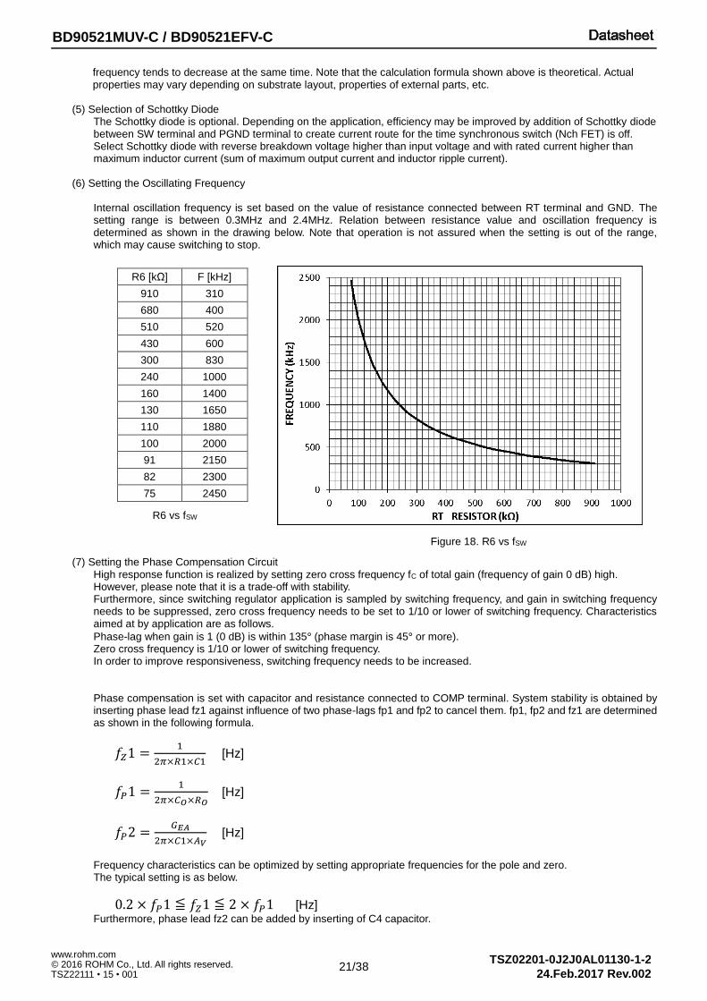
Figure 18. R6 vs fSW
frequency tends to decrease at the same time. Note that the calculation formula shown above is theoretical. Actual properties may vary depending on substrate layout, properties of external parts, etc.
(5) Selection of Schottky Diode
The Schottky diode is optional. Depending on the application, efficiency may be improved by addition of Schottky diode between SW terminal and PGND terminal to create current route for the time synchronous switch (Nch FET) is off. Select Schottky diode with reverse breakdown voltage higher than input voltage and with rated current higher than maximum inductor current (sum of maximum output current and inductor ripple current).
(6) Setting the Oscillating Frequency
Internal oscillation frequency is set based on the value of resistance connected between RT terminal and GND. The setting range is between 0.3MHz and 2.4MHz. Relation between resistance value and oscillation frequency is determined as shown in the drawing below. Note that operation is not assured when the setting is out of the range, which may cause switching to stop.
(7) Setting the Phase Compensation Circuit
High response function is realized by setting zero cross frequency fC of total gain (frequency of gain 0 dB) high. However, please note that it is a trade-off with stability. Furthermore, since switching regulator application is sampled by switching frequency, and gain in switching frequency needs to be suppressed, zero cross frequency needs to be set to 1/10 or lower of switching frequency. Characteristics aimed at by application are as follows.
Phase-lag when gain is 1 (0 dB) is within 135° (phase margin is 45° or more). Zero cross frequency is 1/10 or lower of switching frequency. In order to improve responsiveness, switching frequency needs to be increased.
Phase compensation is set with capacitor and resistance connected to COMP terminal. System stability is obtained by inserting phase lead fz1 against influence of two phase-lags fp1 and fp2 to cancel them. fp1, fp2 and fz1 are determined as shown in the following formula.
𝑓𝑍1 =1
2𝜋×𝑅1×𝐶1 [Hz]
𝑓𝑃1 =1
2𝜋×𝐶𝑂×𝑅𝑂 [Hz]
𝑓𝑃2 =𝐺𝐸𝐴
2𝜋×𝐶1×𝐴𝑉 [Hz]
Frequency characteristics can be optimized by setting appropriate frequencies for the pole and zero. The typical setting is as below.
0.2 × 𝑓𝑃1 ≦ 𝑓𝑍1 ≦ 2 × 𝑓𝑃1 [Hz] Furthermore, phase lead fz2 can be added by inserting of C4 capacitor.
R6 [kΩ] F [kHz]
910 310
680 400
510 520
430 600
300 830
240 1000
160 1400
130 1650
110 1880
100 2000
91 2150
82 2300
75 2450
22/38
TSZ02201-0J2J0AL01130-1-2 24.Feb.2017 Rev.002
BD90521MUV-C / BD90521EFV-C
© 2016 ROHM Co., Ltd. All rights reserved. www.rohm.com
TSZ22111 • 15 • 001
[s]
𝑓Z2 =1
2𝜋×𝑅3×𝐶4 [Hz]
Where:
𝑅𝑂 is the resistance assumed actual load[Ω] = Output Voltage[V] / Output Current[A]、
𝐺𝐸𝐴 is the Error Amp Transconductance (310 µA / V)
𝐴𝑉 is the Error Amp Voltage Gain (60 dB)
Setting Phase Compensation Circuit
Actually, characteristics will vary depending on PCB layout, arrangement of wiring, kinds of parts used and use
conditions (temperature, etc.). Be sure to check stability and responsiveness with actual apparatus. Gain phase
analyzer or FRA is used to check frequency characteristics with actual apparatus. Contact the measurement apparatus
manufacturer for measurement method, etc. When these measurement apparatuses are not available, there is a
method of assuming margin by load response. Variation of output when the apparatus shifts from no load state to
maximum load is monitored, and it can be said that responsiveness is low if variation amount is large, and phase margin
is small if ringing occurs frequently (twice or more as a guide) after variation.
However, confirmation of quantitative phase margin is not possible.
Measurement of Load Response (8) Setting the Soft Start Time
Soft start is necessary for prevention of overshoot of output voltage at startup. Soft start time varies depending on capacitance value of capacitor connected between “SS” terminal and “GND” terminal. Set the startup time on input voltages, VIN and PVIN, earlier than soft start time. Capacitance value of 2200pF to 0.047μF is recommended.
𝑻𝑺𝑺 = 𝑪𝟑 × 𝟎. 𝟔
|𝑰𝒔𝒔|
(9) Setting the Input filter (RIN, CIN2)
Since VIN is used as power source voltage for internal control circuit, input filter for VIN terminal is necessary in order to prevent malfunction due to transient VIN variation. Connect RIN of 10Ω and CIN2 of 1μF. It is necessary to verify under actual use conditions that there is no operation problem such as output off state and overshoot of output due to reduction of VIN during transient response.
Maximum load
Inadequate phase margin
Adequate phase margin.
t
Load
IO
Output voltage
VO
0
Vo
C4
R3
R2
VREF
ERROR AMPLIFIER
COMP
R1
C1
SW L1
CO
RESR RO
Vo
FBR4

23/38
TSZ02201-0J2J0AL01130-1-2 24.Feb.2017 Rev.002
BD90521MUV-C / BD90521EFV-C
© 2016 ROHM Co., Ltd. All rights reserved. www.rohm.com
TSZ22111 • 15 • 001
Recommended Parts Manufacturer List
Shown below is the list of the recommended parts manufacturers for reference.
Type Manufacturer URL
Electrolytic capacitor NICHICON www.nichicon.com
Ceramic capacitor MURATA www.murata.com
Coil TDK www.global.tdk.com
Coil Coilcraft www.coilcraft.com
Coil Sumida www.sumida.com
Diode/Resistor ROHM www.rohm.com

24/38
TSZ02201-0J2J0AL01130-1-2 24.Feb.2017 Rev.002
BD90521MUV-C / BD90521EFV-C
© 2016 ROHM Co., Ltd. All rights reserved. www.rohm.com
TSZ22111 • 15 • 001
Application Examples 1
Parameter Symbol Specification case
Input Voltage VIN 5V
Output Voltage / Output Current VO / IO 1.2V / 2A
Switching Frequency fSW 2.0MHz
Soft Start time TSS 1ms
Operating Temperature Ta -40 to +105°C
No Package Parameters Part Name(series) Type Manufacturer
L1 W6.9 x H7.2 x L4.5 mm3 1μH CLF7045-D Series Inductor TDK
CO1 3216 22μF, X7R, 6.3V GCM Series Ceramic Capacitor MURATA
CO2 3216 22μF, X7R, 6.3V GCM Series Ceramic Capacitor MURATA
CIN1 3225 22μF, X7R, 10V GCM Series Ceramic Capacitor MURATA
CIN2 1608 1μF, X7R, 16V GCM Series Ceramic Capacitor MURATA
CIN3 - - - - -
CIN4 1608 0.01μF, X7R, 50V GCM Series Ceramic Capacitor MURATA
RIN 1608 10Ω, 1%, 1/16W MCR03 Series Chip resistor ROHM
R0 - SHORT - - -
R1 1608 10kΩ, 1%, 1/16W MCR03 Series Chip resistor ROHM
R2 1608 30kΩ, 1%, 1/16W MCR03 Series Chip resistor ROHM
R3 1608 30kΩ, 1%, 1/16W MCR03 Series Chip resistor ROHM
R4 - - - - -
R5 1608 10kΩ, 1%, 1/16W MCR03 Series Chip resistor ROHM
R6 1608 100kΩ, 1%, 1/16W MCR03 Series Chip resistor ROHM
C1 1608 2200pF, R, 50V GCM Series Ceramic Capacitor MURATA
C2 - - - - -
C3 1608 3300pF, R, 50V GCM Series Ceramic Capacitor MURATA
C4 - - - - -
SW
SW
N.C
PVIN
PVIN
SEL
RT
N.C
FB
SS
CO
MP
GN
D
CTL1
EN
VIN
SYN
C
CTL2
PG
OO
D
PG
ND
PG
ND
L1
R2C3
Vo
R5
R1 R6
Co1 Co2
RIN CIN4CIN1
CIN2
C1
CIN3
R3
R4
C4
R0
VINorEN
C2

25/38
TSZ02201-0J2J0AL01130-1-2 24.Feb.2017 Rev.002
BD90521MUV-C / BD90521EFV-C
© 2016 ROHM Co., Ltd. All rights reserved. www.rohm.com
TSZ22111 • 15 • 001
Reference data of Application Example 1
0
10
20
30
40
50
60
70
80
90
100
0.01 0.10 1.00 10.00
Eff
icie
ncy (
%)
Output Load (A)
Figure 20. Loop Response, IO = 2A
Figure 21. Load Response, IO=0A⇔2A
VO (100mV/div)
IO (1A/div)
Figure 22. Load Response, IO=1A⇔2A
VO (100mV/div)
IO (1A/div)
Figure 19. Efficiency vs Output Load
Output Load (A)

26/38
TSZ02201-0J2J0AL01130-1-2 24.Feb.2017 Rev.002
BD90521MUV-C / BD90521EFV-C
© 2016 ROHM Co., Ltd. All rights reserved. www.rohm.com
TSZ22111 • 15 • 001
Application Examples 2
Parameter Symbol Specification case
Input Voltage VIN 5V
Output Voltage / Output Current VO / IO 3.3V / 2A
Switching Frequency fSW 2.0MHz
Soft Start time TSS 1ms
Operating Temperature Ta -40 to +105°C
(Note) Please set to 45kΩ to combine 30 kΩ and 15 kΩ about R3.
No Package Parameters Part Name(series) Type Manufacturer
L1 W6.9 x H7.2 x L4.5 mm3 1μH CLF7045-D Series Inductor TDK
CO1 3216 22μF, X7R, 6.3V GCM Series Ceramic Capacitor MURATA
CO2 3216 22μF, X7R, 6.3V GCM Series Ceramic Capacitor MURATA
CIN1 3225 22μF, X7R, 10V GCM Series Ceramic Capacitor MURATA
CIN2 1608 1μF, X7R, 16V GCM Series Ceramic Capacitor MURATA
CIN3 - - - - -
CIN4 1608 0.01μF, X7R, 50V GCM Series Ceramic Capacitor MURATA
RIN 1608 10Ω, 1%, 1/16W MCR03 Series Chip resistor ROHM
R0 - SHORT - - -
R1 1608 20kΩ, 1%, 1/16W MCR03 Series Chip resistor ROHM
R2 1608 10kΩ, 1%, 1/16W MCR03 Series Chip resistor ROHM
R3 (1) 1608 30kΩ, 1%, 1/16W MCR03 Series Chip resistor ROHM
R3 (2) 1608 15kΩ, 1%, 1/16W MCR03 Series Chip resistor ROHM
R4 - - - - -
R5 1608 10kΩ, 1%, 1/16W MCR03 Series Chip resistor ROHM
R6 1608 100kΩ, 1%, 1/16W MCR03 Series Chip resistor ROHM
C1 1608 2200pF, R, 50V GCM Series Ceramic Capacitor MURATA
C2 - - - - -
C3 1608 3300pF, R, 50V GCM Series Ceramic Capacitor MURATA
C4 - - - - -
SW
SW
N.C
PVIN
PVIN
SEL
RT
N.C
FB
SS
CO
MP
GN
D
CTL1
EN
VIN
SYN
C
CTL2
PG
OO
D
PG
ND
PG
ND
L1
R2C3
Vo
R5
R6
Co1 Co2
RIN CIN4CIN1
CIN2
CIN3
R3
R4
C4
R0
VINorEN
R1
C1 C2
27/38
TSZ02201-0J2J0AL01130-1-2 24.Feb.2017 Rev.002
BD90521MUV-C / BD90521EFV-C
© 2016 ROHM Co., Ltd. All rights reserved. www.rohm.com
TSZ22111 • 15 • 001
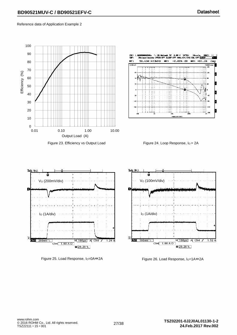
Reference data of Application Example 2
0
10
20
30
40
50
60
70
80
90
100
0.01 0.10 1.00 10.00
Eff
icie
ncy (%
)
Output Load (A)
Figure 24. Loop Response, IO = 2A
Figure 25. Load Response, IO=0A⇔2A
VO (200mV/div)
IO (1A/div)
Figure 26. Load Response, IO=1A⇔2A
VO (100mV/div)
IO (1A/div)
Figure 23. Efficiency vs Output Load

28/38
TSZ02201-0J2J0AL01130-1-2 24.Feb.2017 Rev.002
BD90521MUV-C / BD90521EFV-C
© 2016 ROHM Co., Ltd. All rights reserved. www.rohm.com
TSZ22111 • 15 • 001
Notes on the PCB Layout
Exposed die pad is needed to be connected to GND.
Application Circuit (VQFN20SV4040)
Exposed die pad is needed to be connected to GND.
Application Circuit (HTSSOP-B20)
① Make bold line part as short as possible in wide pattern.
② Arrange input ceramic capacitors CIN1, CIN3 and CIN4 as close as possible to PVIN terminal and PGND terminal. Arrange CIN2 as close as possible to VIN terminal and GND terminal.
③ Arrange R6 as close as possible to RT terminal.
④ Arrange R2 and R3 as close as possible to FB terminal to shorten wirings from R2 and R3 to FB terminal.
⑤ Arrange R2 and R3 as far as possible from L1.
⑥ Influence of SW noise can be reduced by separating power system (input/output capacitor) GND from reference system
(RT, COMP) GND. Connect them in common GND layers as shown in the layout in the next section.
⑦ R0 is for measurement of frequency characteristics of feedback and is optional.
Insertion of resistance in R0 enables measurement of frequency characteristics of feedback (phase margin) using FRA, etc. Under normal conditions, it is shorted.
SW
SW
N.C
PVIN
PVIN
SEL
RT
N.C
FB
SS
CO
MP
GN
D
CT
L1
EN
VIN
SY
NC
CT
L2
PG
OO
D
PG
ND
PG
ND
L1
R2C3
Vo
R5
R6
Co1 Co2
RIN CIN1
R3
R4
C4
R0
VIN
or
EN
CIN3 CIN4
CIN2
R1
C1 C2
SW
SW
N.C
PVIN
PVIN
SEL
RT
N.C
FB
SS
PGND
PGND PGOOD
CTL2
SYNC
VIN
EN
CTL1
COMP
GND
VIN or EN
L1Vo
Co1 Co2
RINCIN4
CIN1
CIN2
CIN3
R2C3R1 R6
C1
R3
R4
C4
R0
C2
R5

29/38
TSZ02201-0J2J0AL01130-1-2 24.Feb.2017 Rev.002
BD90521MUV-C / BD90521EFV-C
© 2016 ROHM Co., Ltd. All rights reserved. www.rohm.com
TSZ22111 • 15 • 001
Reference layout pattern
TOP Layer Middle 1 Layer
Middle 2 Layer Bottom Layer
R0
L1
VO
GND
VIN
GND
PGOOD
SYNC EN
SEL
CO1
CIN1
CO2
R5
R6 C4 R4
R3 R2 C3
C1 C2
R1 CIN2
RIN
CIN3 CIN4
IC
VQFN20SV4040 Reference PCB Layout (TOP VIEW)

30/38
TSZ02201-0J2J0AL01130-1-2 24.Feb.2017 Rev.002
BD90521MUV-C / BD90521EFV-C
© 2016 ROHM Co., Ltd. All rights reserved. www.rohm.com
TSZ22111 • 15 • 001
Middle 1 Layer TOP Layer
HTSSOP-B20 Reference PCB Layout (TOP VIEW)
L1
VO
GND
VIN
GND
PGOOD
SYNC EN
SEL
CO1
IC
CIN1
CO2
R5
R6 C4 R4
R3 R2 C3
C1 C2
R1 CIN2
RIN CIN3 CIN4
Middle 2 Layer Bottom Layer
R0

31/38
TSZ02201-0J2J0AL01130-1-2 24.Feb.2017 Rev.002
BD90521MUV-C / BD90521EFV-C
© 2016 ROHM Co., Ltd. All rights reserved. www.rohm.com
TSZ22111 • 15 • 001
Power Dissipation
In thermal design, operate under following conditions. (Temperatures described below are guaranteed temperatures. Be sure to consider margin, etc.)
1. Ambient temperature Ta shall be 125°C or lower.
2. Chip junction temperature Tj shall be 150°C or lower.
Chip junction temperature Tj can be considered in following 2 ways.
① When obtained from temperature Tt at the center of top surface of package under actual use conditions:
𝑇𝑗 = 𝑇𝑡 + 𝜓𝐽𝑇 × 𝑃𝑇𝑂𝑇𝐴𝐿
② When obtained from actual ambient temperature Ta:
𝑇𝑗 = 𝑇𝑎 + 𝜃𝑗𝑎 × 𝑃𝑇𝑂𝑇𝐴𝐿
<Reference Value>VQFN020SV4040 <Reference Value>HTSSOP-B20
θjc θjc Top : 40 °C /W Top : 25 °C /W Bottom : 15 °C /W Bottom : 9 °C /W θjc θjc 153.9 °C / W 1-layer PCB 143.0 °C / W 1-layer PCB 37.4 °C / W 4-layer PCB 26.8 °C / W 4-layer PCB ψJT ψJT
13 °C /W 1-layer PCB 8 °C /W 1-layer PCB 7 °C /W 4-layer PCB 4 °C /W 4-layer PCB PCB Size 114.3 mm x 76.2 mm x 1.6 mm PCB Size 114.3 mm x 76.2 mm x 1.6 mm
The heat loss PTOTAL of the IC can be obtained by the formula shown below:
𝑃𝑇𝑂𝑇𝐴𝐿 = 𝑃𝐼𝐶𝐶 + 𝑃𝑅𝑂𝑁 + 𝑃𝑆𝑊 [W]
𝑃𝐼𝐶𝐶=𝑉𝐼𝑁× 𝐼𝐼𝑁 [W] ⋯ Heat dissipation in control circuit
𝑃𝑅𝑂𝑁 = 𝑅𝑂𝑁 × 𝐼𝑂2
[W] ⋯ Heat dissipation in output FET
𝑅𝑂𝑁 = 𝐷 × 𝑅𝑂𝑁_𝑆𝑊_𝐻 + (1 − 𝐷) × 𝑅𝑂𝑁_𝑆𝑊_𝐿 [Ω] ⋯ On Resistance in output FET
𝐷 =𝑉𝑂
𝑉𝐼𝑁 ⋯ Switching pulse duty
𝑃𝑆𝑊 = 𝑡𝑟 × 𝐼𝑂 × 𝑉𝐼𝑁 × 𝑓𝑆𝑊 [W] ⋯ eat dissipation in switching
𝑊ℎ𝑒𝑟𝑒 ∶
𝑉𝐼𝑁 is the input voltage [V]
𝐼𝐼𝑁 is the circuit current [A]
𝐼𝑂 is the load current [A]
𝐷 is the switching pulse duty
𝑅𝑂𝑁_𝑆𝑊_𝐻 is the H-side FET ON resistance [Ω]
𝑅𝑂𝑁_𝑆𝑊_𝐿 is the L-side FET ON resistance [Ω]
𝑇𝑟 is the switching rise and fall time [S] (Typ:7ns) 𝑓𝑆𝑊 is the oscillating frequency [Hz]

32/38
TSZ02201-0J2J0AL01130-1-2 24.Feb.2017 Rev.002
BD90521MUV-C / BD90521EFV-C
© 2016 ROHM Co., Ltd. All rights reserved. www.rohm.com
TSZ22111 • 15 • 001
I/O Equivalent Circuits
SW EN, SEL
COMP SS
FB RT
SYNC PGOOD
PVIN
SW
PGND
VIN
COMP
GND
VIN
SS
GND
VIN
FB
GND
VIN
RT
GND
VIN
SYNC
GND
PGOOD
GND
EN
SEL
GND

33/38
TSZ02201-0J2J0AL01130-1-2 24.Feb.2017 Rev.002
BD90521MUV-C / BD90521EFV-C
© 2016 ROHM Co., Ltd. All rights reserved. www.rohm.com
TSZ22111 • 15 • 001
Operational Notes
1. Reverse Connection of Power Supply
Connecting the power supply in reverse polarity can damage the IC. Take precautions against reverse polarity when connecting the power supply, such as mounting an external diode between the power supply and the IC’s power supply pins.
2. Power Supply Lines
Design the PCB layout pattern to provide low impedance supply lines. Separate the ground and supply lines of the digital and analog blocks to prevent noise in the ground and supply lines of the digital block from affecting the analog block. Furthermore, connect a capacitor to ground at all power supply pins. Consider the effect of temperature and aging on the capacitance value when using electrolytic capacitors.
3. Ground Voltage
Ensure that no pins are at a voltage below that of the ground pin at any time, even during transient condition.
4. Ground Wiring Pattern
When using both small-signal and large-current ground traces, the two ground traces should be routed separately but connected to a single ground at the reference point of the application board to avoid fluctuations in the small-signal ground caused by large currents. Also ensure that the ground traces of external components do not cause variations on the ground voltage. The ground lines must be as short and thick as possible to reduce line impedance.
5. Thermal Consideration
Should by any chance the maximum junction temperature rating be exceeded the rise in temperature of the chip may result in deterioration of the properties of the chip. In case of exceeding this absolute maximum rating, increase the board size and copper area to prevent exceeding the maximum junction temperature rating.
6. Recommended Operating Conditions
These conditions represent a range within which the expected characteristics of the IC can be approximately obtained. The electrical characteristics are guaranteed under the conditions of each parameter.
7. Inrush Current
When power is first supplied to the IC, it is possible that the internal logic may be unstable and inrush current may flow instantaneously due to the internal powering sequence and delays, especially if the IC has more than one power supply. Therefore, give special consideration to power coupling capacitance, power wiring, width of ground wiring, and routing of connections.
8. Testing on Application Boards
When testing the IC on an application board, connecting a capacitor directly to a low-impedance output pin may subject the IC to stress. Always discharge capacitors completely after each process or step. The IC’s power supply should always be turned off completely before connecting or removing it from the test setup during the inspection process. To prevent damage from static discharge, ground the IC during assembly and use similar precautions during transport and storage.
9. Inter-pin Short and Mounting Errors
Ensure that the direction and position are correct when mounting the IC on the PCB. Incorrect mounting may result in damaging the IC. Avoid nearby pins being shorted to each other especially to ground, power supply and output pin. Inter-pin shorts could be due to many reasons such as metal particles, water droplets (in very humid environment) and unintentional solder bridge deposited in between pins during assembly to name a few.
10. Unused Input Pins
Input pins of an IC are often connected to the gate of a MOS transistor. The gate has extremely high impedance and extremely low capacitance. If left unconnected, the electric field from the outside can easily charge it. The small charge acquired in this way is enough to produce a significant effect on the conduction through the transistor and cause unexpected operation of the IC. So unless otherwise specified, unused input pins should be connected to the power supply or ground line.

34/38
TSZ02201-0J2J0AL01130-1-2 24.Feb.2017 Rev.002
BD90521MUV-C / BD90521EFV-C
© 2016 ROHM Co., Ltd. All rights reserved. www.rohm.com
TSZ22111 • 15 • 001
Operational Notes – continued
11. Regarding the Input Pin of the IC
This monolithic IC contains P+ isolation and P substrate layers between adjacent elements in order to keep them isolated. P-N junctions are formed at the intersection of the P layers with the N layers of other elements, creating a parasitic diode or transistor. For example (refer to figure below):
When GND > Pin A and GND > Pin B, the P-N junction operates as a parasitic diode. When GND > Pin B, the P-N junction operates as a parasitic transistor.
Parasitic diodes inevitably occur in the structure of the IC. The operation of parasitic diodes can result in mutual interference among circuits, operational faults, or physical damage. Therefore, conditions that cause these diodes to operate, such as applying a voltage lower than the GND voltage to an input pin (and thus to the P substrate) should be avoided.
Figure 27. Example of monolithic IC structure
12. Ceramic Capacitor
When using a ceramic capacitor, determine the dielectric constant considering the change of capacitance with temperature and the decrease in nominal capacitance due to DC bias and others.
13. Area of Safe Operation (ASO)
Operate the IC such that the output voltage, output current, and the maximum junction temperature rating are all within the Area of Safe Operation (ASO).
14. Thermal Shutdown Circuit(TSD)
This IC has a built-in thermal shutdown circuit that prevents heat damage to the IC. Normal operation should always be within the IC’s maximum junction temperature rating. If however the rating is exceeded for a continued period, the junction temperature (Tj) will rise which will activate the TSD circuit that will turn OFF all output pins. When the Tj falls below the TSD threshold, the circuits are automatically restored to normal operation. Note that the TSD circuit operates in a situation that exceeds the absolute maximum ratings and therefore, under no circumstances, should the TSD circuit be used in a set design or for any purpose other than protecting the IC from heat damage.
15. Over Current Protection Circuit (OCP)
This IC incorporates an integrated overcurrent protection circuit that is activated when the load is shorted. This protection circuit is effective in preventing damage due to sudden and unexpected incidents. However, the IC should not be used in applications characterized by continuous operation or transitioning of the protection circuit.
N NP
+ P
N NP
+
P Substrate
GND
NP
+
N NP
+N P
P Substrate
GND GND
Parasitic
Elements
Pin A
Pin A
Pin B Pin B
B C
E
Parasitic
Elements
GNDParasitic
Elements
CB
E
Transistor (NPN)Resistor
N Region
close-by
Parasitic
Elements

35/38
TSZ02201-0J2J0AL01130-1-2 24.Feb.2017 Rev.002
BD90521MUV-C / BD90521EFV-C
© 2016 ROHM Co., Ltd. All rights reserved. www.rohm.com
TSZ22111 • 15 • 001
Ordering Information
B D 9 0 5 2 1 M U V - CE 2
Product name Package
MUV : VQFN20SV4040 EFV : HTSSOP-B20
Product rank C: Automotive rank Packaging and forming specification E2: Embossed tape and reel
Marking Diagrams
Marking Package Part Number Marking
90521 VQFN20SV4040 BD90521MUV-CE2
D90521 HTSSOP-B20 BD90521EFV-CE2
VQFN20SV4040 (TOP VIEW)
9 0 5 2 1
Part Number Marking
LOT Number
1PIN MARK
HTSSOP-B20 (TOP VIEW)
D 9 0 5 2 1
Part Number Marking
LOT Number
1PIN MARK
HTSSOP-B20 (TOP VIEW)
D 9 0 5 2 1
Part Number Marking
LOT Number
1PIN MARK

36/38
TSZ02201-0J2J0AL01130-1-2 24.Feb.2017 Rev.002
BD90521MUV-C / BD90521EFV-C
© 2016 ROHM Co., Ltd. All rights reserved. www.rohm.com
TSZ22111 • 15 • 001
Physical Dimension, Tape and Reel Information
Package Name VQFN20SV4040

37/38
TSZ02201-0J2J0AL01130-1-2 24.Feb.2017 Rev.002
BD90521MUV-C / BD90521EFV-C
© 2016 ROHM Co., Ltd. All rights reserved. www.rohm.com
TSZ22111 • 15 • 001
Physical Dimension, Tape and Reel Information
Package Name HTSSOP-B20
38/38
TSZ02201-0J2J0AL01130-1-2 24.Feb.2017 Rev.002
BD90521MUV-C / BD90521EFV-C
© 2016 ROHM Co., Ltd. All rights reserved. www.rohm.com
TSZ22111 • 15 • 001
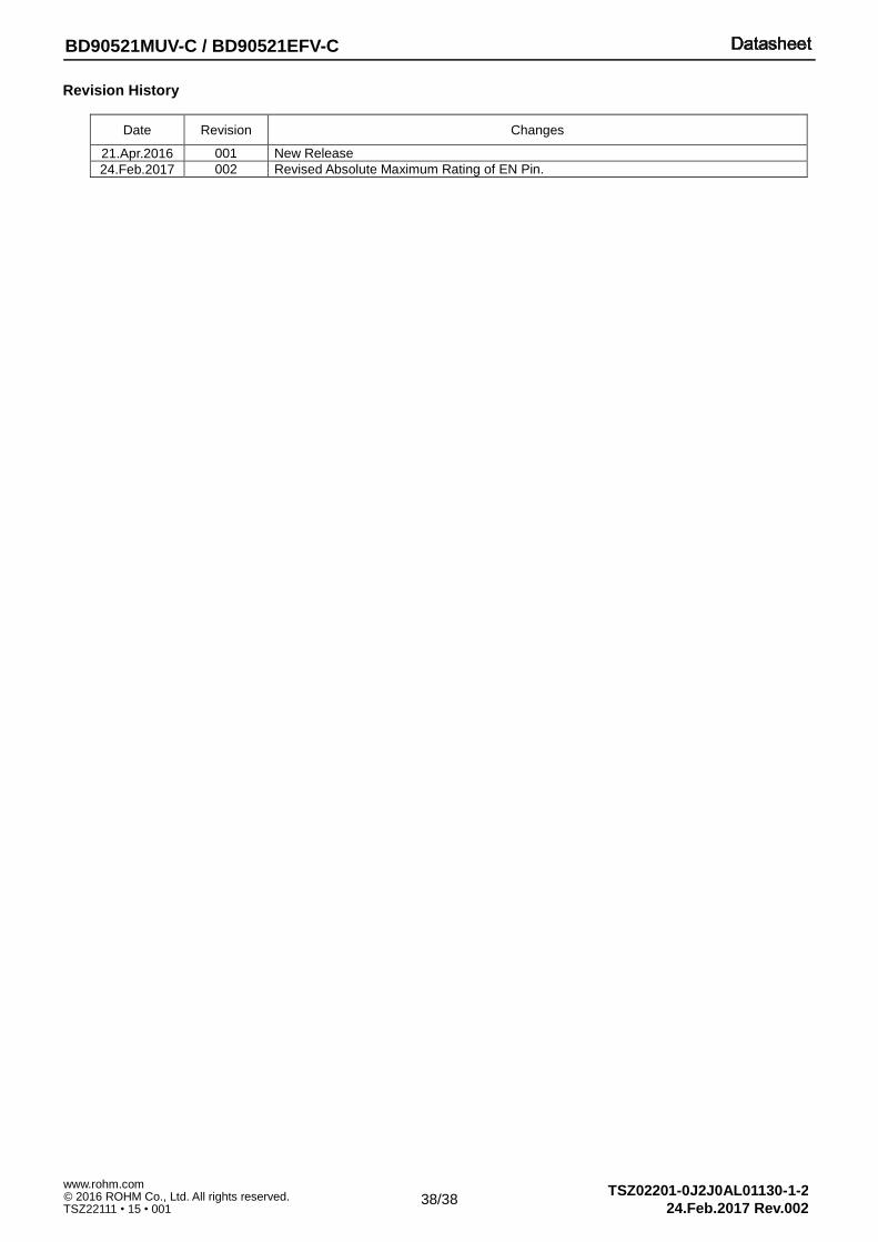
Revision History
Date Revision Changes
21.Apr.2016 001 New Release
24.Feb.2017 002 Revised Absolute Maximum Rating of EN Pin.

Notice-PAA-E Rev.003
© 2015 ROHM Co., Ltd. All rights reserved.
Notice
Precaution on using ROHM Products 1. If you intend to use our Products in devices requiring extremely high reliability (such as medical equipment
(Note 1),
aircraft/spacecraft, nuclear power controllers, etc.) and whose malfunction or failure may cause loss of human life, bodily injury or serious damage to property (“Specific Applications”), please consult with the ROHM sales representative in advance. Unless otherwise agreed in writing by ROHM in advance, ROHM shall not be in any way responsible or liable for any damages, expenses or losses incurred by you or third parties arising from the use of any ROHM’s Products for Specific Applications.
(Note1) Medical Equipment Classification of the Specific Applications
JAPAN USA EU CHINA
CLASSⅢ CLASSⅢ
CLASSⅡb CLASSⅢ
CLASSⅣ CLASSⅢ
2. ROHM designs and manufactures its Products subject to strict quality control system. However, semiconductor
products can fail or malfunction at a certain rate. Please be sure to implement, at your own responsibilities, adequate safety measures including but not limited to fail-safe design against the physical injury, damage to any property, which a failure or malfunction of our Products may cause. The following are examples of safety measures:
[a] Installation of protection circuits or other protective devices to improve system safety [b] Installation of redundant circuits to reduce the impact of single or multiple circuit failure
3. Our Products are not designed under any special or extraordinary environments or conditions, as exemplified below. Accordingly, ROHM shall not be in any way responsible or liable for any damages, expenses or losses arising from the use of any ROHM’s Products under any special or extraordinary environments or conditions. If you intend to use our Products under any special or extraordinary environments or conditions (as exemplified below), your independent verification and confirmation of product performance, reliability, etc, prior to use, must be necessary:
[a] Use of our Products in any types of liquid, including water, oils, chemicals, and organic solvents [b] Use of our Products outdoors or in places where the Products are exposed to direct sunlight or dust [c] Use of our Products in places where the Products are exposed to sea wind or corrosive gases, including Cl2,
H2S, NH3, SO2, and NO2
[d] Use of our Products in places where the Products are exposed to static electricity or electromagnetic waves [e] Use of our Products in proximity to heat-producing components, plastic cords, or other flammable items [f] Sealing or coating our Products with resin or other coating materials [g] Use of our Products without cleaning residue of flux (even if you use no-clean type fluxes, cleaning residue of
flux is recommended); or Washing our Products by using water or water-soluble cleaning agents for cleaning residue after soldering
[h] Use of the Products in places subject to dew condensation
4. The Products are not subject to radiation-proof design. 5. Please verify and confirm characteristics of the final or mounted products in using the Products. 6. In particular, if a transient load (a large amount of load applied in a short period of time, such as pulse. is applied,
confirmation of performance characteristics after on-board mounting is strongly recommended. Avoid applying power exceeding normal rated power; exceeding the power rating under steady-state loading condition may negatively affect product performance and reliability.
7. De-rate Power Dissipation depending on ambient temperature. When used in sealed area, confirm that it is the use in
the range that does not exceed the maximum junction temperature. 8. Confirm that operation temperature is within the specified range described in the product specification. 9. ROHM shall not be in any way responsible or liable for failure induced under deviant condition from what is defined in
this document.
Precaution for Mounting / Circuit board design 1. When a highly active halogenous (chlorine, bromine, etc.) flux is used, the residue of flux may negatively affect product
performance and reliability. 2. In principle, the reflow soldering method must be used on a surface-mount products, the flow soldering method must
be used on a through hole mount products. If the flow soldering method is preferred on a surface-mount products, please consult with the ROHM representative in advance.
For details, please refer to ROHM Mounting specification

Notice-PAA-E Rev.003
© 2015 ROHM Co., Ltd. All rights reserved.
Precautions Regarding Application Examples and External Circuits 1. If change is made to the constant of an external circuit, please allow a sufficient margin considering variations of the
characteristics of the Products and external components, including transient characteristics, as well as static characteristics.
2. You agree that application notes, reference designs, and associated data and information contained in this document
are presented only as guidance for Products use. Therefore, in case you use such information, you are solely responsible for it and you must exercise your own independent verification and judgment in the use of such information contained in this document. ROHM shall not be in any way responsible or liable for any damages, expenses or losses incurred by you or third parties arising from the use of such information.
Precaution for Electrostatic This Product is electrostatic sensitive product, which may be damaged due to electrostatic discharge. Please take proper caution in your manufacturing process and storage so that voltage exceeding the Products maximum rating will not be applied to Products. Please take special care under dry condition (e.g. Grounding of human body / equipment / solder iron, isolation from charged objects, setting of Ionizer, friction prevention and temperature / humidity control).
Precaution for Storage / Transportation 1. Product performance and soldered connections may deteriorate if the Products are stored in the places where:
[a] the Products are exposed to sea winds or corrosive gases, including Cl2, H2S, NH3, SO2, and NO2 [b] the temperature or humidity exceeds those recommended by ROHM [c] the Products are exposed to direct sunshine or condensation [d] the Products are exposed to high Electrostatic
2. Even under ROHM recommended storage condition, solderability of products out of recommended storage time period may be degraded. It is strongly recommended to confirm solderability before using Products of which storage time is exceeding the recommended storage time period.
3. Store / transport cartons in the correct direction, which is indicated on a carton with a symbol. Otherwise bent leads
may occur due to excessive stress applied when dropping of a carton. 4. Use Products within the specified time after opening a humidity barrier bag. Baking is required before using Products of
which storage time is exceeding the recommended storage time period.
Precaution for Product Label A two-dimensional barcode printed on ROHM Products label is for ROHM’s internal use only.
Precaution for Disposition When disposing Products please dispose them properly using an authorized industry waste company.
Precaution for Foreign Exchange and Foreign Trade act Since concerned goods might be fallen under listed items of export control prescribed by Foreign exchange and Foreign trade act, please consult with ROHM in case of export.
Precaution Regarding Intellectual Property Rights 1. All information and data including but not limited to application example contained in this document is for reference
only. ROHM does not warrant that foregoing information or data will not infringe any intellectual property rights or any other rights of any third party regarding such information or data.
2. ROHM shall not have any obligations where the claims, actions or demands arising from the combination of the Products with other articles such as components, circuits, systems or external equipment (including software).
3. No license, expressly or implied, is granted hereby under any intellectual property rights or other rights of ROHM or any third parties with respect to the Products or the information contained in this document. Provided, however, that ROHM will not assert its intellectual property rights or other rights against you or your customers to the extent necessary to manufacture or sell products containing the Products, subject to the terms and conditions herein.
Other Precaution 1. This document may not be reprinted or reproduced, in whole or in part, without prior written consent of ROHM.
2. The Products may not be disassembled, converted, modified, reproduced or otherwise changed without prior written consent of ROHM.
3. In no event shall you use in any way whatsoever the Products and the related technical information contained in the Products or this document for any military purposes, including but not limited to, the development of mass-destruction weapons.
4. The proper names of companies or products described in this document are trademarks or registered trademarks of ROHM, its affiliated companies or third parties.

DatasheetDatasheet
Notice – WE Rev.001© 2015 ROHM Co., Ltd. All rights reserved.
General Precaution 1. Before you use our Pro ducts, you are requested to care fully read this document and fully understand its contents.
ROHM shall n ot be in an y way responsible or liabl e for fa ilure, malfunction or acci dent arising from the use of a ny ROHM’s Products against warning, caution or note contained in this document.
2. All information contained in this docume nt is current as of the issuing date and subj ect to change without any prior
notice. Before purchasing or using ROHM’s Products, please confirm the la test information with a ROHM sale s representative.
3. The information contained in this doc ument is provi ded on an “as is” basis and ROHM does not warrant that all
information contained in this document is accurate an d/or error-free. ROHM shall not be in an y way responsible or liable for any damages, expenses or losses incurred by you or third parties resulting from inaccuracy or errors of or concerning such information.