Basic Semiconductor Devices - Carleton Universitytjs/4700_pdf/LecPhys9.pdf · Basic Semiconductor...
45
Basic Semiconductor Devices BJT, MosFET, LED, Laser and Solar Cells and photo-detectors. Fig 6.1 From Principles of Electronic Materials and Devices, Third Edition, S.O. Kasap (© McGraw-Hill, 2005)
Transcript of Basic Semiconductor Devices - Carleton Universitytjs/4700_pdf/LecPhys9.pdf · Basic Semiconductor...
Basic Semiconductor Devices
BJT, MosFET, LED, Laser and Solar Cells and photo-detectors.
Fig 6.1
From Principles of Electronic Materials and Devices, Third Edition, S.O. Kasap (© McGraw-Hill, 2005)

BJT Structure
Basic BJT structure is three terminal device used for switching and amplification. Two flavors npn and pnp – both back to back diodes with depletion regions.
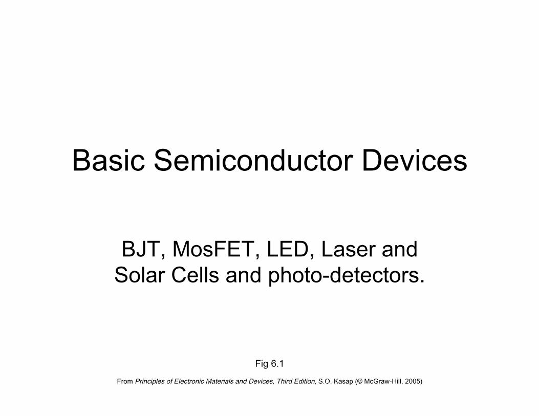
Band Diagrams (In equilibrium)
Ec
Ev
Ef
Emitter Base Collector
N P N
Ec
Ev
Ef
Emitter Base Collector
N P N
• In equilibrium EF must be flat – this creates depletion regions and barriers.
• For normal operation – EBJ forward biased
• Barrier reduced and so electrons diffuse into the base
• Electrons get swept across the base into the collector
– CBJ reverse biased • Electrons roll down the
hill (high E-field)

Minority Carrier Concentration Profiles
• Current dominated by injection of electrons from emitter to base (by design) – Back injection from base to emitter is small as we use a N+PN diode
• The forward bias EBJ and diffusion of the minority carrier concentration causes a gradient (diffusion) through the base:
– some recombination causes bowing of electron concentration (in the base) – base is designed to be fairly short (minimize recombination)
• Drift currents are usually small and neglected
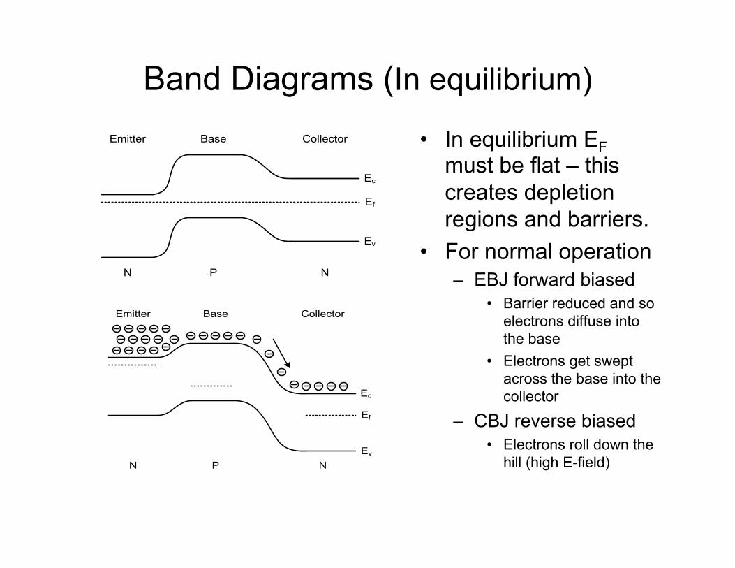
Diffusion Current Through the Base
• Diffusion of electrons through the base is set by concentration profile at the EBJ
• “Law of the junction” sets the concentrations of the minority carriers at edges of the base region
lllllll
• Diffusion current of electrons through the base is (assuming an ideal straight line case):
• Due to back injection and recombination in the base, the current at the EBJ and current at the CBJ are not equal and differ by a base current
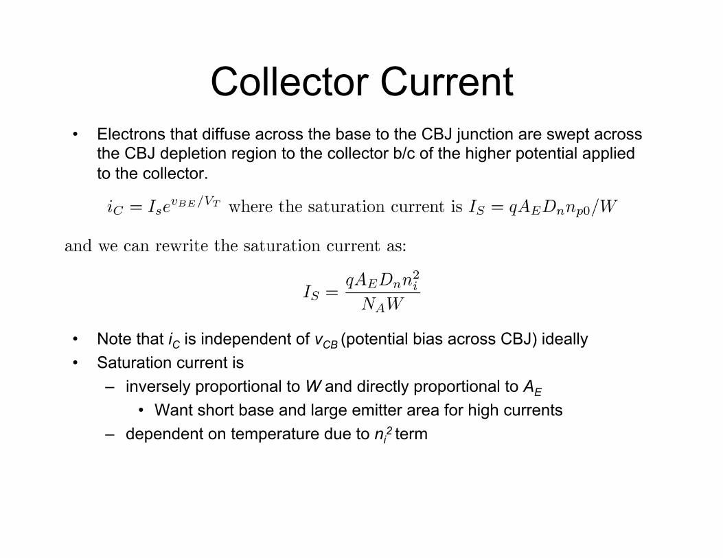
Collector Current • Electrons that diffuse across the base to the CBJ junction are swept across
the CBJ depletion region to the collector b/c of the higher potential applied to the collector.
• Note that iC is independent of vCB (potential bias across CBJ) ideally • Saturation current is
– inversely proportional to W and directly proportional to AE
• Want short base and large emitter area for high currents – dependent on temperature due to ni
2 term

Base Current • Base current iB composed of two components:
– holes back injected from the base region into the emitter region
– holes supplied due to recombination in the base with diffusing electrons and depends on minority carrier lifetime τb in the base
And the Q in the base is
So, current is
• Total base current is

Beta and Emitter Current • Can relate iB and iC by the following
equation and β is
– Beta is constant for a particular transistor
– On the order of 100-200 in modern devices (but can be higher)
– Called the common-emitter current gain
• For high current gain, want small W, low NA, high ND
• Emitter current is the sum of iC and iBα is called the common-base current gain
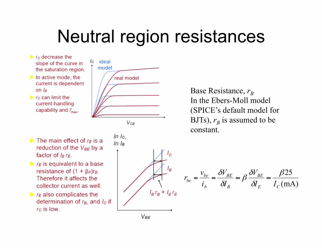
Neutral region resistances
Base Resistance, rB In the Ebers-Moll model (SPICE’s default model for BJTs), rB is assumed to be constant.
)mA(25
CE
BE
B
BE
b
bebe II
VIV
ivr β
δδ
βδδ
≈≈==
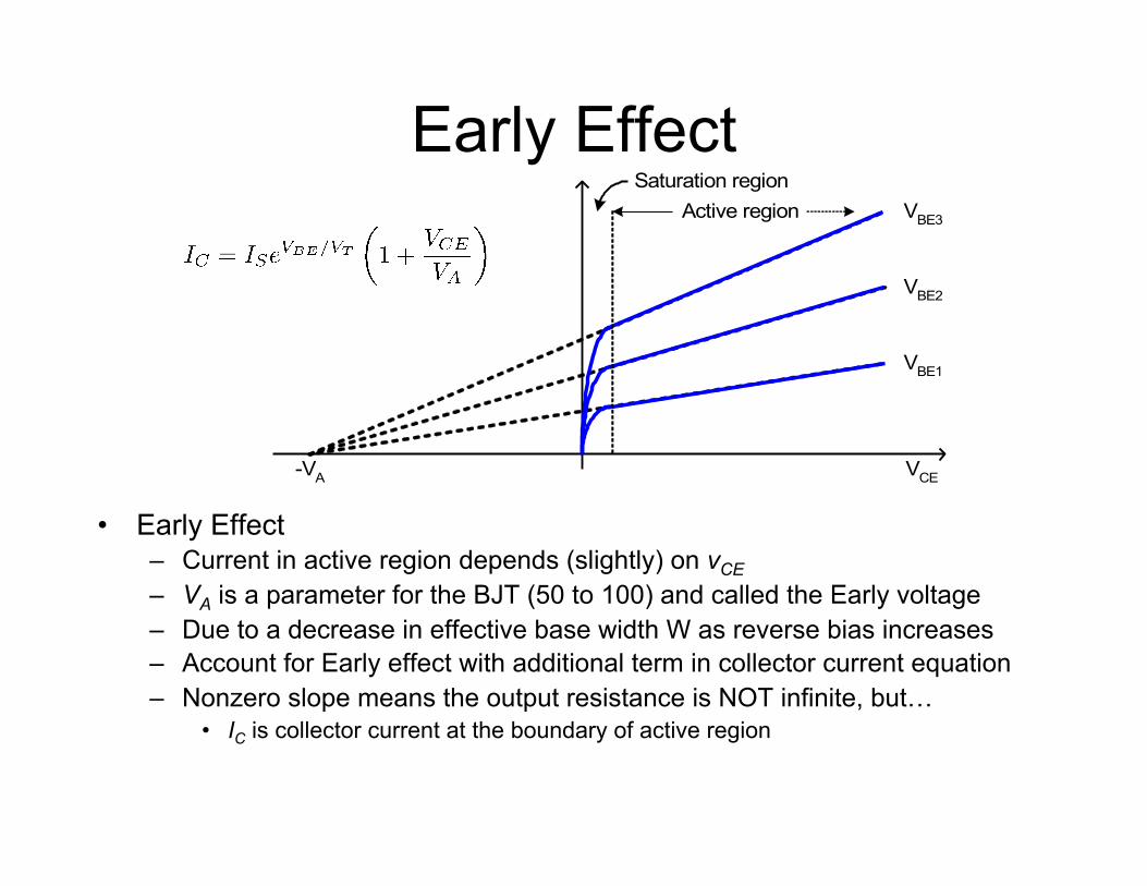
Early Effect
• Early Effect – Current in active region depends (slightly) on vCE – VA is a parameter for the BJT (50 to 100) and called the Early voltage – Due to a decrease in effective base width W as reverse bias increases – Account for Early effect with additional term in collector current equation – Nonzero slope means the output resistance is NOT infinite, but…
• IC is collector current at the boundary of active region
VCE
VBE1
VBE2
VBE3Active regionSaturation region
-VA
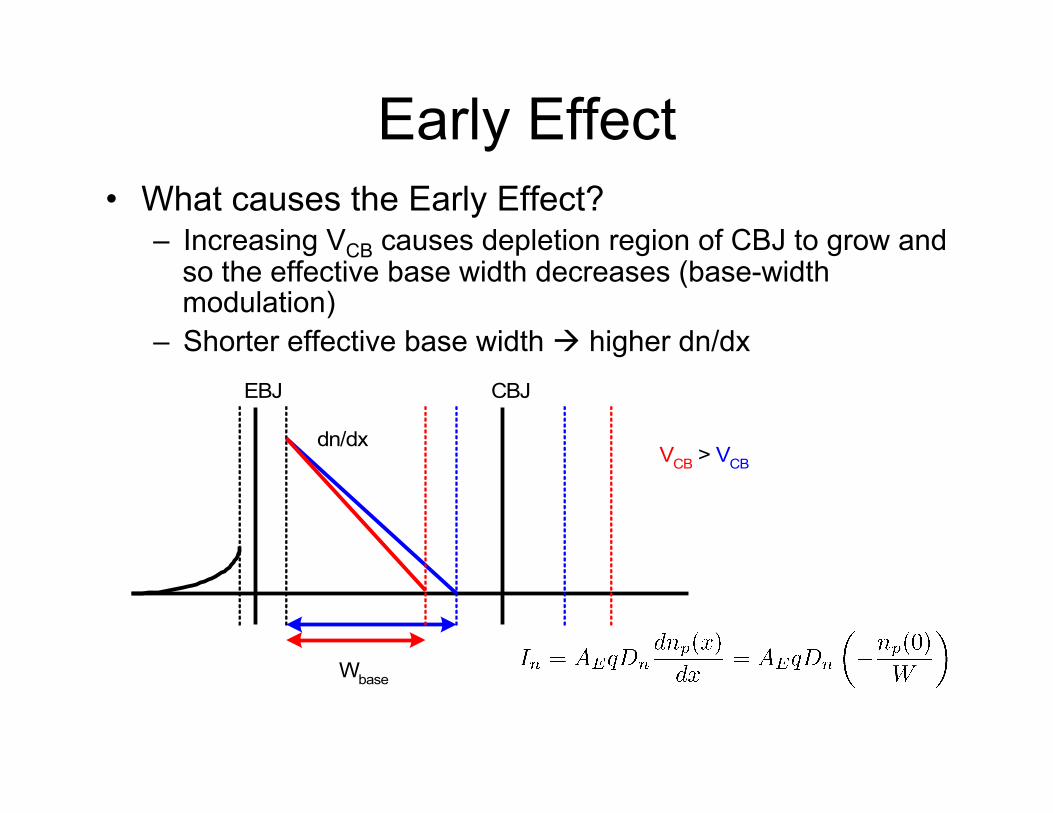
Early Effect • What causes the Early Effect?
– Increasing VCB causes depletion region of CBJ to grow and so the effective base width decreases (base-width modulation)
– Shorter effective base width à higher dn/dx EBJ CBJ
dn/dxVCB > VCB
Wbase
From Principles of Electronic Materials and Devices, Third Edition, S.O. Kasap (© McGraw-Hill, 2005)
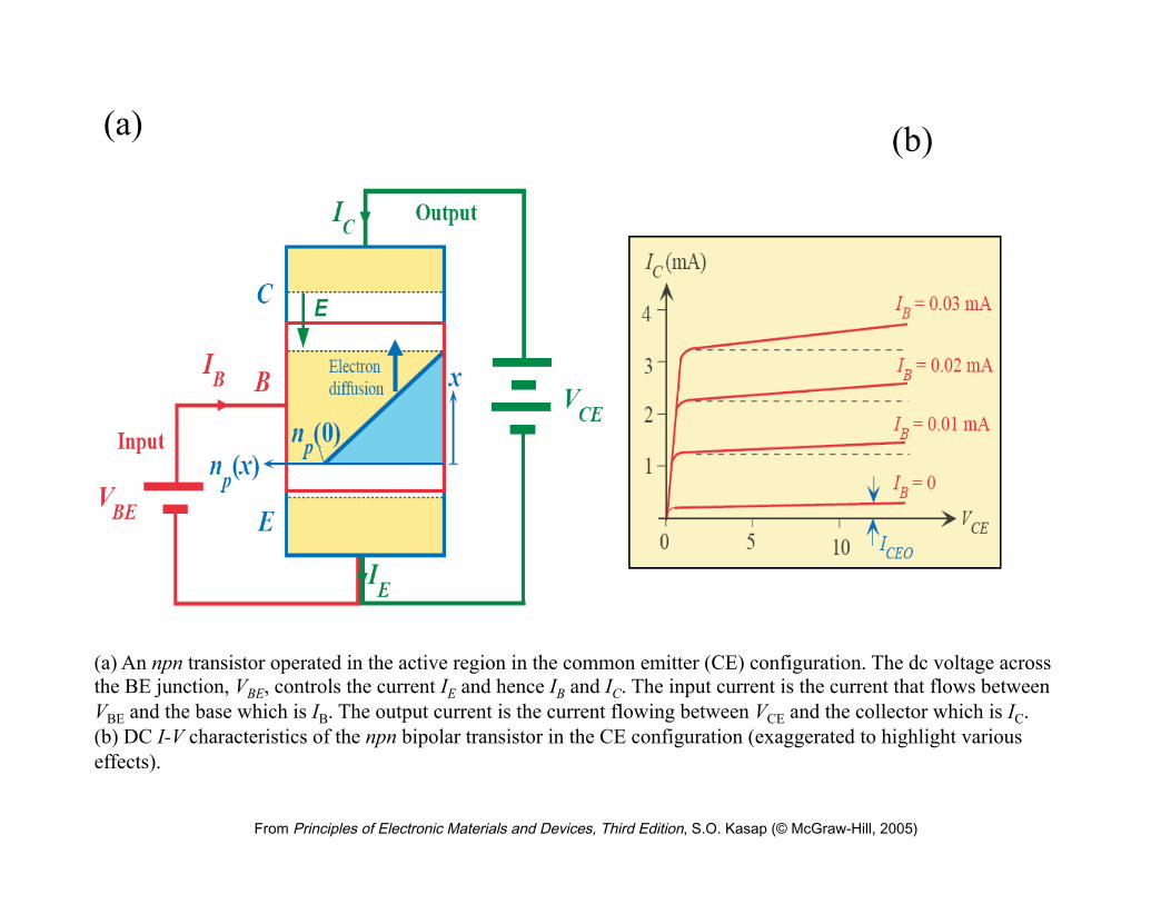
(a) An npn transistor operated in the active region in the common emitter (CE) configuration. The dc voltage across the BE junction, VBE, controls the current IE and hence IB and IC. The input current is the current that flows between VBE and the base which is IB. The output current is the current flowing between VCE and the collector which is IC. (b) DC I-V characteristics of the npn bipolar transistor in the CE configuration (exaggerated to highlight various effects).
(a) (b)

Fig 6.26
From Principles of Electronic Materials and Devices, Third Edition, S.O. Kasap (© McGraw-Hill, 2005)
Ebors Moll Model
Need to add depletion and diffusion capacitances and worry about breakdown.
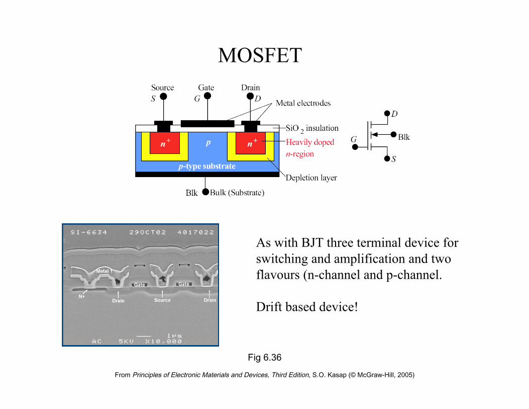
Fig 6.36
From Principles of Electronic Materials and Devices, Third Edition, S.O. Kasap (© McGraw-Hill, 2005)
MOSFET
As with BJT three terminal device for switching and amplification and two flavours (n-channel and p-channel. Drift based device!
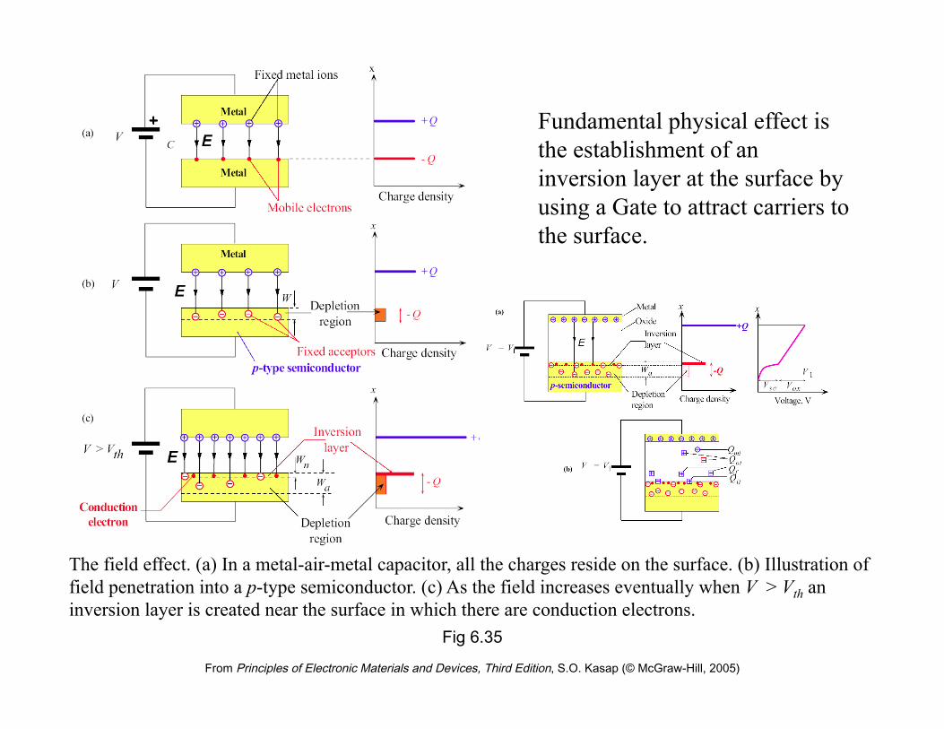
Fig 6.35
From Principles of Electronic Materials and Devices, Third Edition, S.O. Kasap (© McGraw-Hill, 2005)
The field effect. (a) In a metal-air-metal capacitor, all the charges reside on the surface. (b) Illustration of field penetration into a p-type semiconductor. (c) As the field increases eventually when V > Vth an inversion layer is created near the surface in which there are conduction electrons.
Fundamental physical effect is the establishment of an inversion layer at the surface by using a Gate to attract carriers to the surface.
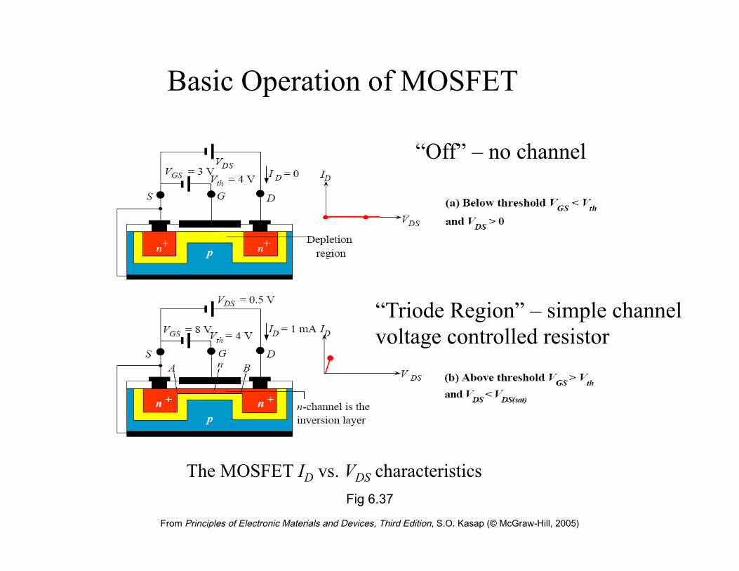
Fig 6.37
From Principles of Electronic Materials and Devices, Third Edition, S.O. Kasap (© McGraw-Hill, 2005)
The MOSFET ID vs. VDS characteristics
Basic Operation of MOSFET
“Off” – no channel
“Triode Region” – simple channel voltage controlled resistor
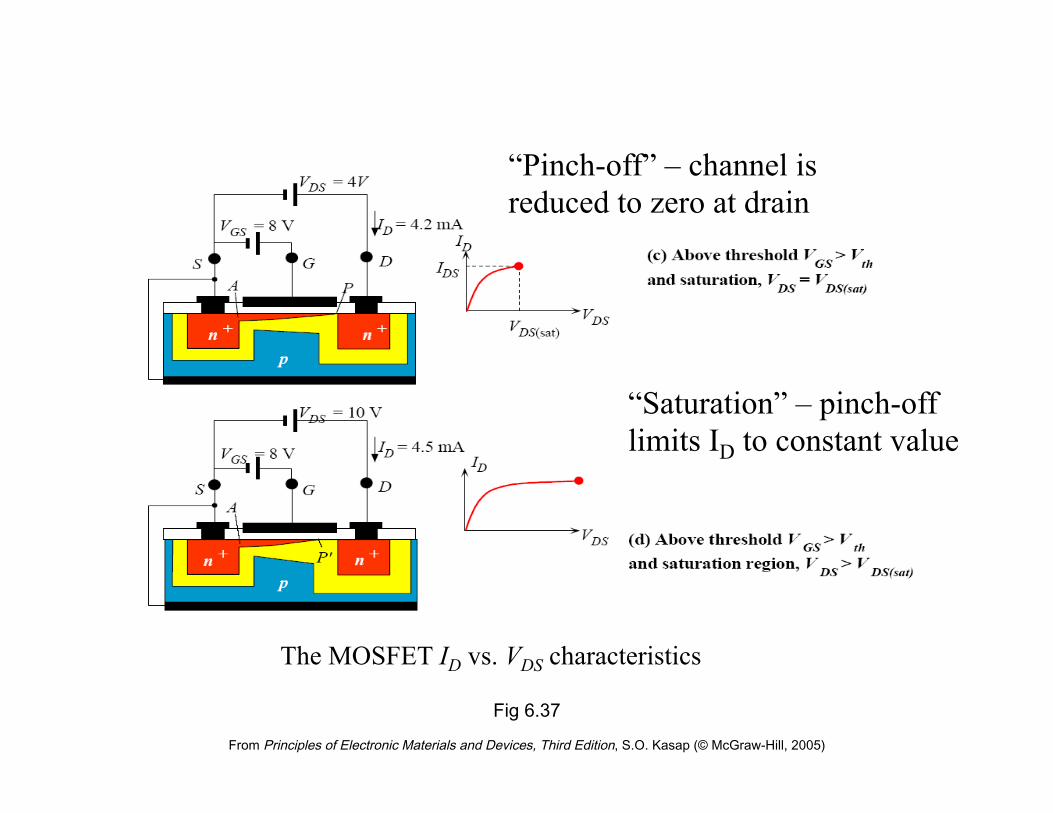
Fig 6.37
From Principles of Electronic Materials and Devices, Third Edition, S.O. Kasap (© McGraw-Hill, 2005)
The MOSFET ID vs. VDS characteristics
“Pinch-off” – channel is reduced to zero at drain
“Saturation” – pinch-off limits ID to constant value
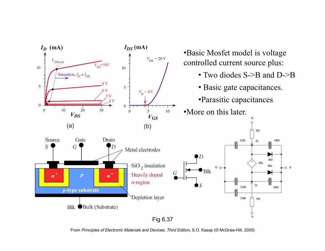
Fig 6.37
From Principles of Electronic Materials and Devices, Third Edition, S.O. Kasap (© McGraw-Hill, 2005)
• Basic Mosfet model is voltage controlled current source plus:
• Two diodes S->B and D->B • Basic gate capacitances. • Parasitic capacitances
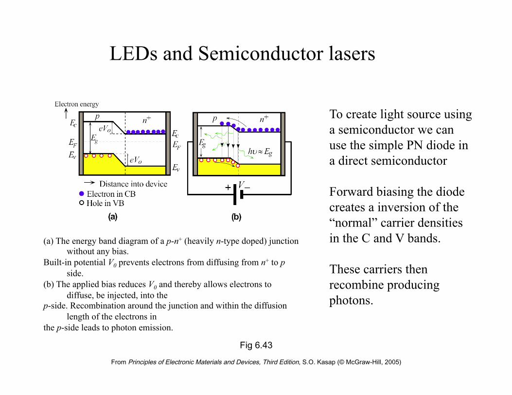
Fig 6.43
From Principles of Electronic Materials and Devices, Third Edition, S.O. Kasap (© McGraw-Hill, 2005)
(a) The energy band diagram of a p-n+ (heavily n-type doped) junction without any bias.
Built-in potential V0 prevents electrons from diffusing from n+ to p side.
(b) The applied bias reduces V0 and thereby allows electrons to diffuse, be injected, into the
p-side. Recombination around the junction and within the diffusion length of the electrons in
the p-side leads to photon emission.
LEDs and Semiconductor lasers
To create light source using a semiconductor we can use the simple PN diode in a direct semiconductor Forward biasing the diode creates a inversion of the “normal” carrier densities in the C and V bands. These carriers then recombine producing photons.
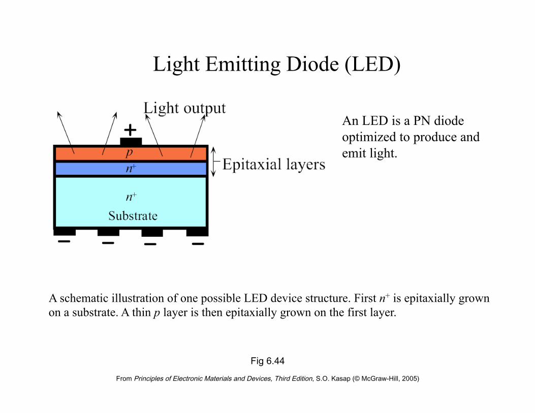
Fig 6.44
From Principles of Electronic Materials and Devices, Third Edition, S.O. Kasap (© McGraw-Hill, 2005)
A schematic illustration of one possible LED device structure. First n+ is epitaxially grown on a substrate. A thin p layer is then epitaxially grown on the first layer.
An LED is a PN diode optimized to produce and emit light.
Light Emitting Diode (LED)
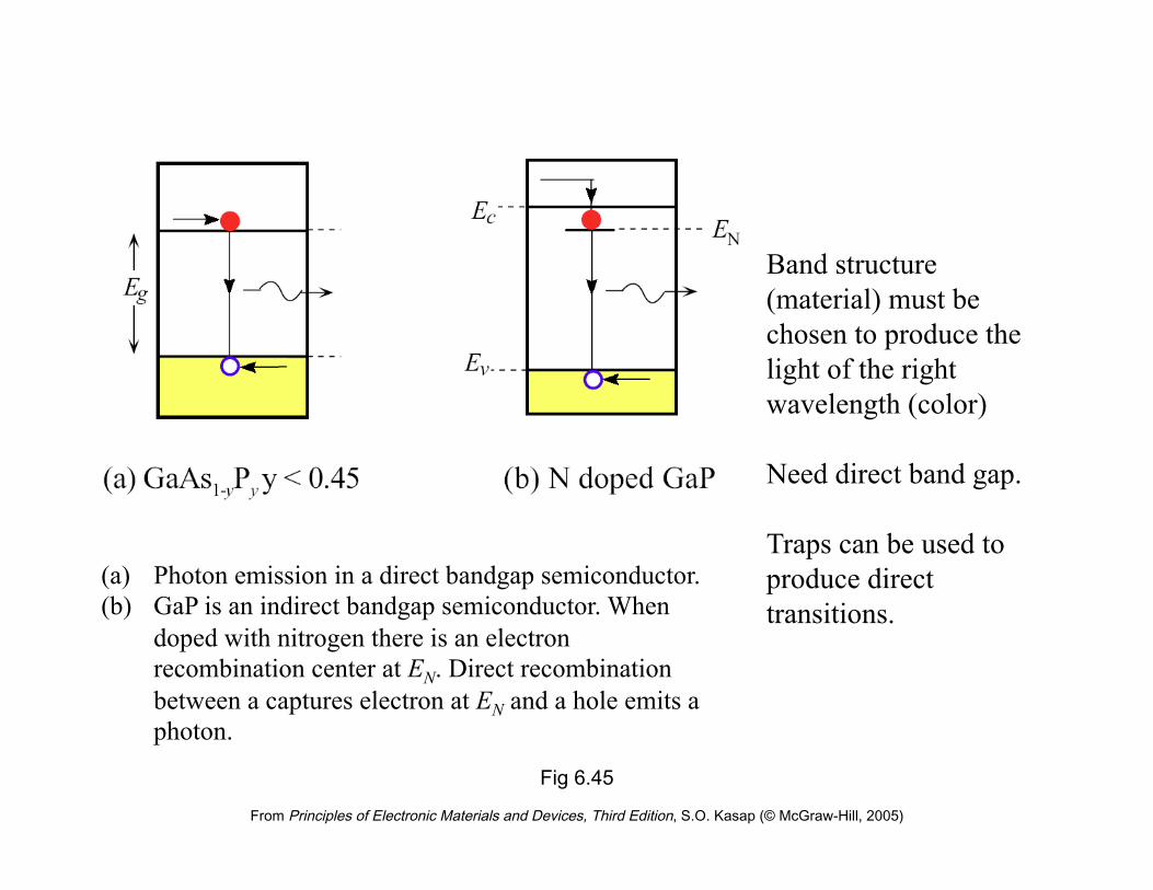
Fig 6.45
From Principles of Electronic Materials and Devices, Third Edition, S.O. Kasap (© McGraw-Hill, 2005)
(a) Photon emission in a direct bandgap semiconductor. (b) GaP is an indirect bandgap semiconductor. When
doped with nitrogen there is an electron recombination center at EN. Direct recombination between a captures electron at EN and a hole emits a photon.
Band structure (material) must be chosen to produce the light of the right wavelength (color) Need direct band gap. Traps can be used to produce direct transitions.
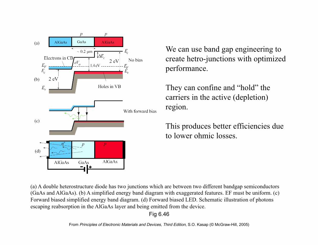
Fig 6.46
From Principles of Electronic Materials and Devices, Third Edition, S.O. Kasap (© McGraw-Hill, 2005)
(a) A double heterostructure diode has two junctions which are between two different bandgap semiconductors (GaAs and AlGaAs). (b) A simplified energy band diagram with exaggerated features. EF must be uniform. (c) Forward biased simplified energy band diagram. (d) Forward biased LED. Schematic illustration of photons escaping reabsorption in the AlGaAs layer and being emitted from the device.
We can use band gap engineering to create hetro-junctions with optimized performance. They can confine and “hold” the carriers in the active (depletion) region. This produces better efficiencies due to lower ohmic losses.

Fig 6.47
From Principles of Electronic Materials and Devices, Third Edition, S.O. Kasap (© McGraw-Hill, 2005)
Fig 6.48
From Principles of Electronic Materials and Devices, Third Edition, S.O. Kasap (© McGraw-Hill, 2005)
Due to 3/2kT spread in electron/hole energies there are variety of transitions that can occur. The light is therefore not absolutely monochromatic but has a band-width. IV characteristic is just the ideal diode equation. Light production is linearly related to I.
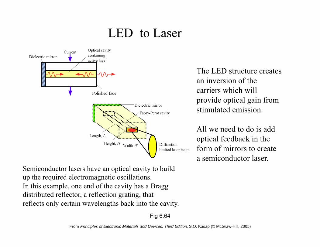
Fig 6.64
From Principles of Electronic Materials and Devices, Third Edition, S.O. Kasap (© McGraw-Hill, 2005)
Semiconductor lasers have an optical cavity to build up the required electromagnetic oscillations. In this example, one end of the cavity has a Bragg distributed reflector, a reflection grating, that reflects only certain wavelengths back into the cavity.
LED to Laser
The LED structure creates an inversion of the carriers which will provide optical gain from stimulated emission. All we need to do is add optical feedback in the form of mirrors to create a semiconductor laser.
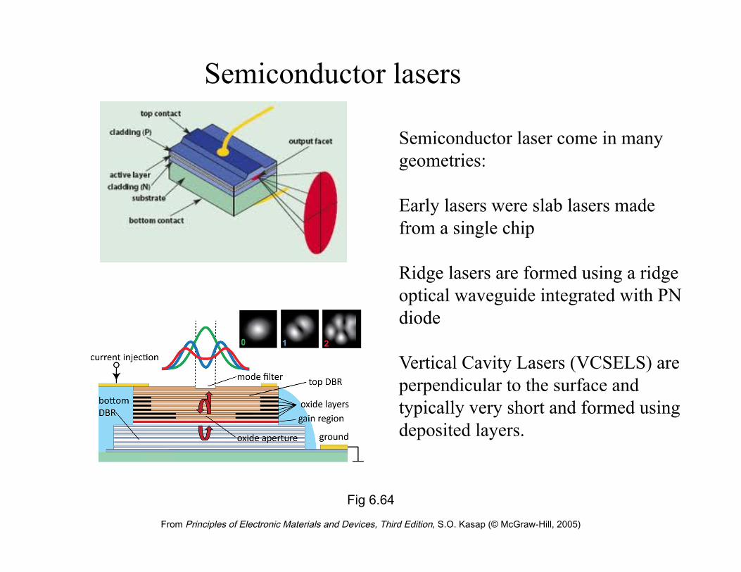
Fig 6.64
From Principles of Electronic Materials and Devices, Third Edition, S.O. Kasap (© McGraw-Hill, 2005)
Semiconductor lasers
Semiconductor laser come in many geometries: Early lasers were slab lasers made from a single chip Ridge lasers are formed using a ridge optical waveguide integrated with PN diode Vertical Cavity Lasers (VCSELS) are perpendicular to the surface and typically very short and formed using deposited layers.
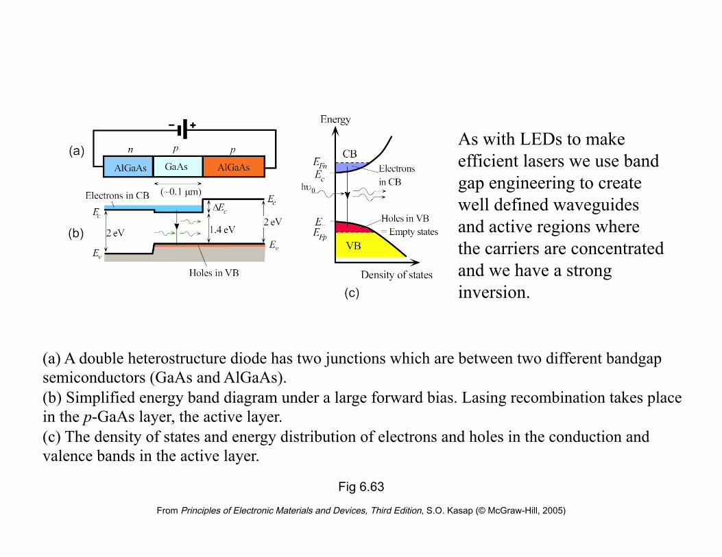
Fig 6.63
From Principles of Electronic Materials and Devices, Third Edition, S.O. Kasap (© McGraw-Hill, 2005)
(a) A double heterostructure diode has two junctions which are between two different bandgap semiconductors (GaAs and AlGaAs). (b) Simplified energy band diagram under a large forward bias. Lasing recombination takes place in the p-GaAs layer, the active layer. (c) The density of states and energy distribution of electrons and holes in the conduction and valence bands in the active layer.
As with LEDs to make efficient lasers we use band gap engineering to create well defined waveguides and active regions where the carriers are concentrated and we have a strong inversion.
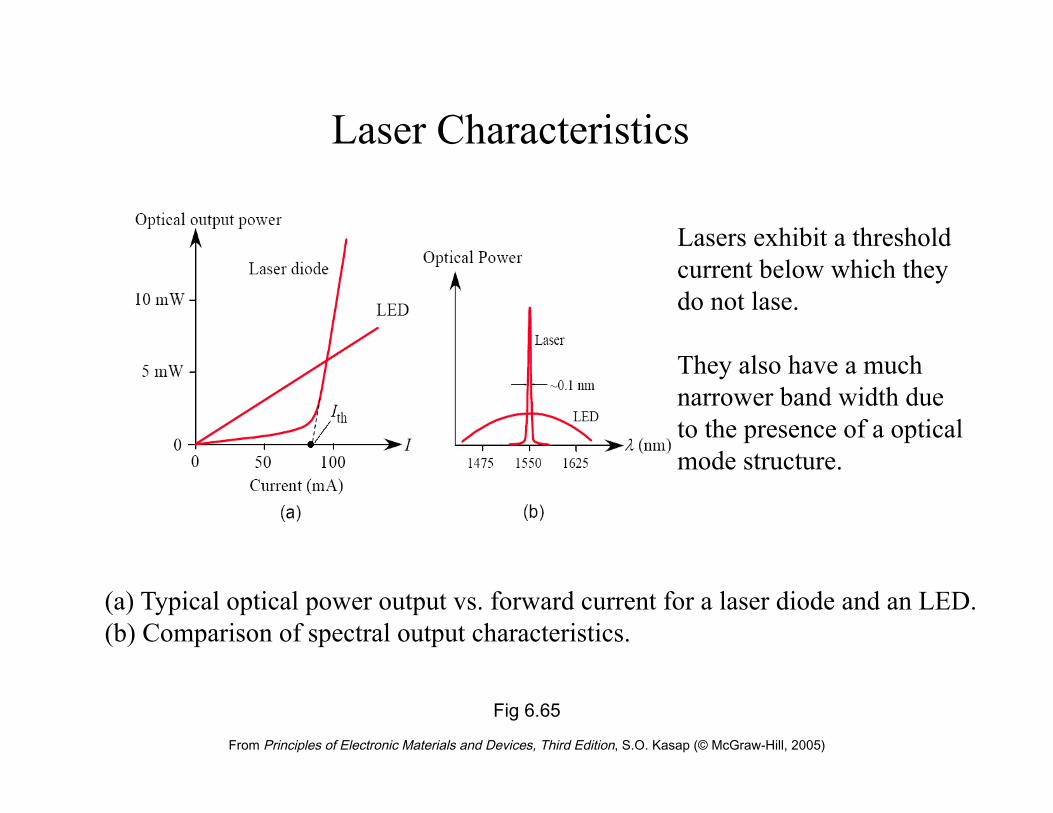
Fig 6.65
From Principles of Electronic Materials and Devices, Third Edition, S.O. Kasap (© McGraw-Hill, 2005)
(a) Typical optical power output vs. forward current for a laser diode and an LED. (b) Comparison of spectral output characteristics.
Lasers exhibit a threshold current below which they do not lase. They also have a much narrower band width due to the presence of a optical mode structure.
Laser Characteristics

Laser Modeling
From Principles of Electronic Materials and Devices, Third Edition, S.O. Kasap (© McGraw-Hill, 2005)
• Many types of lasers: slab, ridge, VCSEL • Complicated geometry • Complicated band-structures • Complicated operation
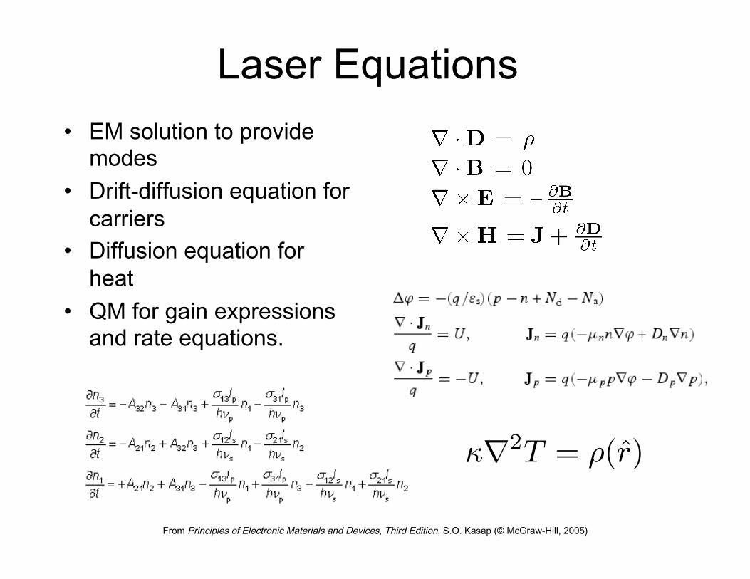
Laser Equations
From Principles of Electronic Materials and Devices, Third Edition, S.O. Kasap (© McGraw-Hill, 2005)
• EM solution to provide modes
• Drift-diffusion equation for carriers
• Diffusion equation for heat
• QM for gain expressions and rate equations.
r2T = ⇢(r̂)

Coupling of the Equations • Optical propagation equations are primarily determined
by neff(x,y,z) (index of refraction) and G(x,y,z) (optical gain fct). Both of these are a function of N(x,y,z) (electron density)
• N(x,y,z) is fct of T, J (current density) and photon density
• Temperature equation is driven by heat generation which is fct of J
• J is fct of applied potential and temperature • Rather complicated! • Approaches usually make approximations and
simplifications.
From Principles of Electronic Materials and Devices, Third Edition, S.O. Kasap (© McGraw-Hill, 2005)

Detailed Laser Modeling
• Detailed device modeling usually attempts to solve a particular aspect: – Optical modes – Electron transport and photon
generation – Thermal effects
• Example is optical modes for different geometries.
From Principles of Electronic Materials and Devices, Third Edition, S.O. Kasap (© McGraw-Hill, 2005)
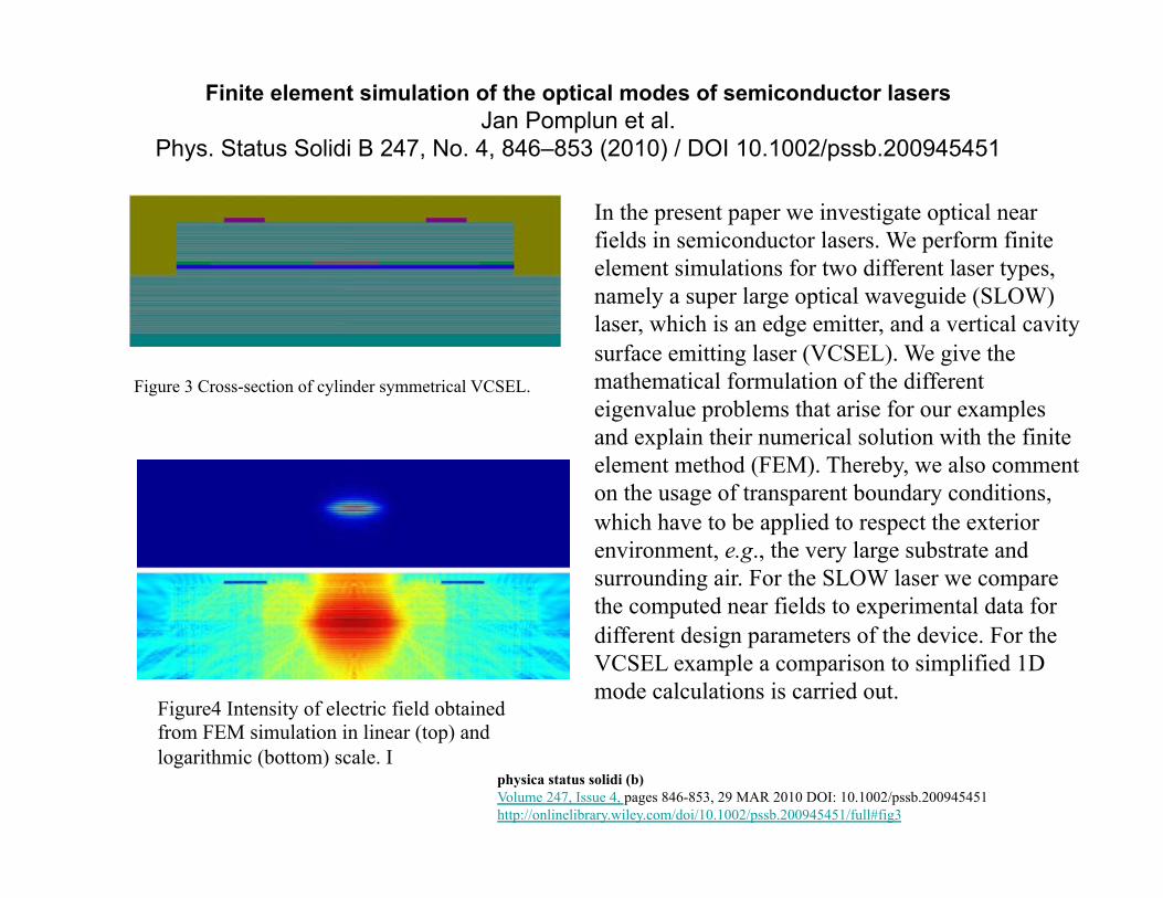
Finite element simulation of the optical modes of semiconductor lasers Jan Pomplun et al.
Phys. Status Solidi B 247, No. 4, 846–853 (2010) / DOI 10.1002/pssb.200945451
physica status solidi (b) Volume 247, Issue 4, pages 846-853, 29 MAR 2010 DOI: 10.1002/pssb.200945451 http://onlinelibrary.wiley.com/doi/10.1002/pssb.200945451/full#fig3
In the present paper we investigate optical near fields in semiconductor lasers. We perform finite element simulations for two different laser types, namely a super large optical waveguide (SLOW) laser, which is an edge emitter, and a vertical cavity surface emitting laser (VCSEL). We give the mathematical formulation of the different eigenvalue problems that arise for our examples and explain their numerical solution with the finite element method (FEM). Thereby, we also comment on the usage of transparent boundary conditions, which have to be applied to respect the exterior environment, e.g., the very large substrate and surrounding air. For the SLOW laser we compare the computed near fields to experimental data for different design parameters of the device. For the VCSEL example a comparison to simplified 1D mode calculations is carried out.
Figure 3 Cross-section of cylinder symmetrical VCSEL.
Figure4 Intensity of electric field obtained from FEM simulation in linear (top) and logarithmic (bottom) scale. I

Finite element simulation of the optical modes of semiconductor lasers
physica status solidi (b) Volume 247, Issue 4, pages 846-853, 29 MAR 2010 DOI: 10.1002/pssb.200945451 http://onlinelibrary.wiley.com/doi/10.1002/pssb.200945451/full#fig3
Figure 6 Finite element triangulation of cross-section of SLOW laser. The meaning of the parameters w and d is also indicated.
Figure 10 Intensity of fundamental lasing mode for varying w1⁄42.2, 9.0, 15.0 mm. Gold trenches and active layer are shown in green and red, respectively.
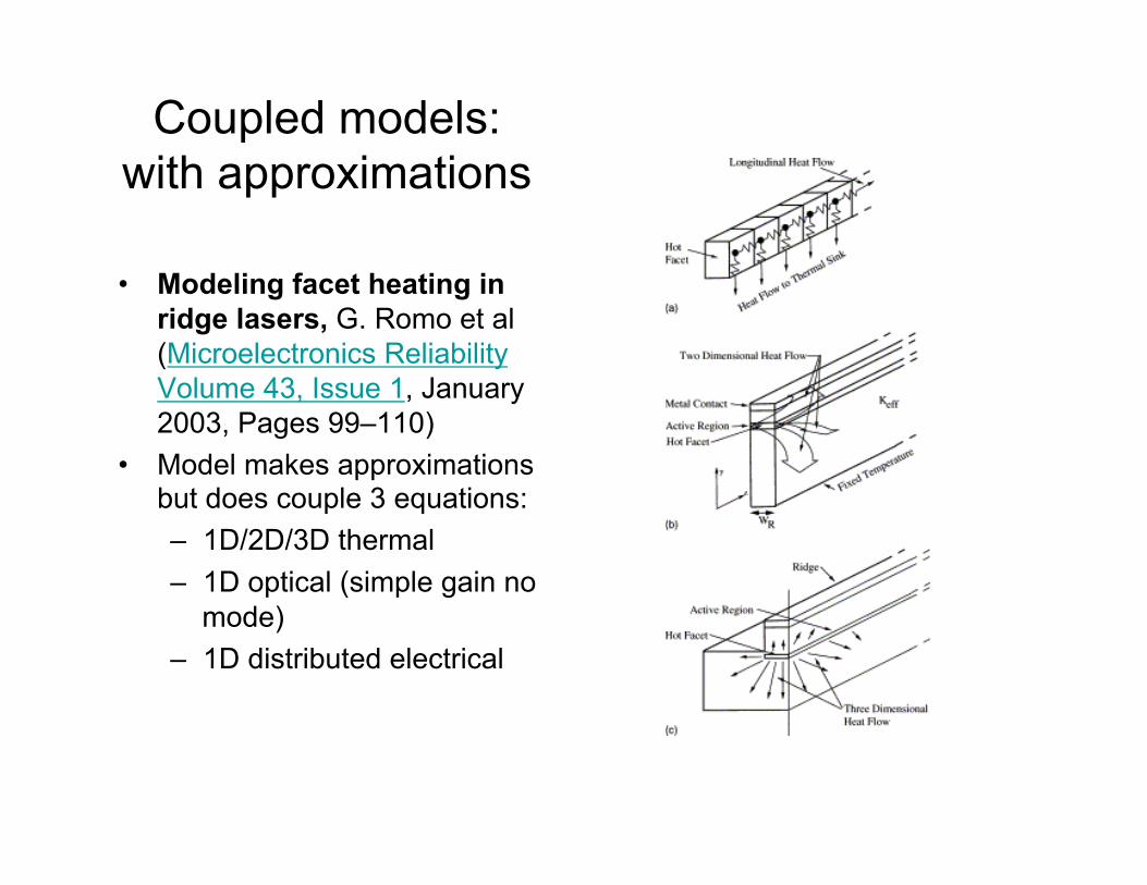
Coupled models: with approximations
• Modeling facet heating in ridge lasers, G. Romo et al (Microelectronics Reliability Volume 43, Issue 1, January 2003, Pages 99–110)
• Model makes approximations but does couple 3 equations: – 1D/2D/3D thermal – 1D optical (simple gain no
mode) – 1D distributed electrical

Equations • Optical intensity (I)
equation is 1D. With 2 equation for forward and backwards
• Electron density equation (n) includes diffusion (1D).
• Gain expression
• Thermal equation is 3D • Thermal heating includes
ohmic generation and optical heating at the facet.

2D and 3D temperature distributions
1D and 2D heat flow models are bad. Generally heat flow is 3D processes and it is difficult to approximate the geometry.
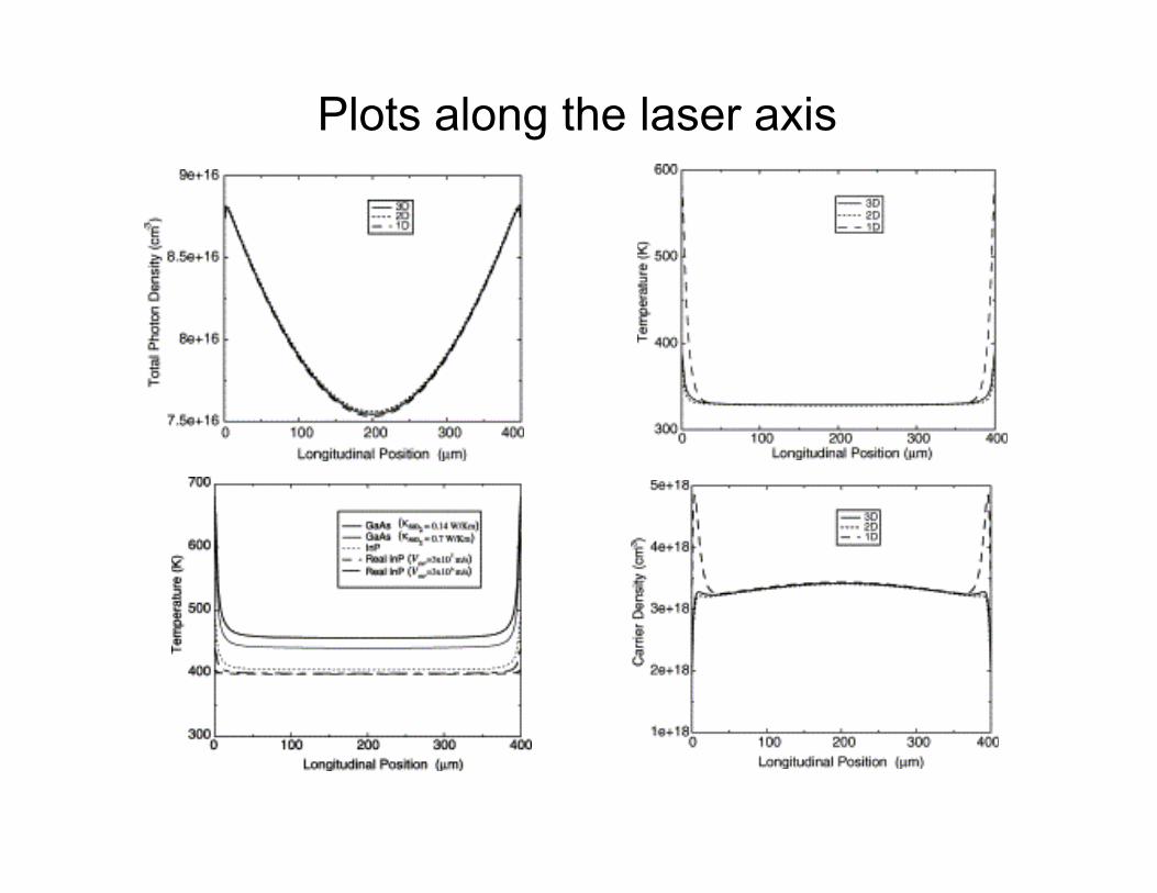
Plots along the laser axis

From Principles of Electronic Materials and Devices, Third Edition, S.O. Kasap (© McGraw-Hill, 2005)
dN
dt=
⌘(Id
� Ioff
)
qVl
� N
⌧n
� G0(N �N0)Pi
1 + ✏P
dP
dt=
�G0(N �N0)P
1 + ✏P� P
⌧p
+��N
⌧n
d�
dt=
1
2↵(�G0(N �N0)� 1
⌧p
)
Rate Equations • The simplest effective model is a three rate equation model. • Three variables are:
• N – Electron density • P – Photon density • Φ – Optical phase
• Driving by diode current. • Three coupled non-linear 1st order differential equations. • Very complicated behaviour • Characterized by photon and electron lifetimes, optical gain and offset current
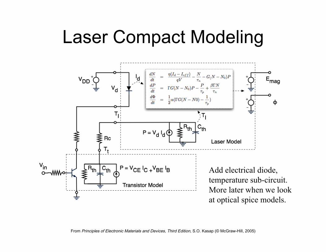
Laser Compact Modeling
From Principles of Electronic Materials and Devices, Third Edition, S.O. Kasap (© McGraw-Hill, 2005)
Add electrical diode, temperature sub-circuit. More later when we look at optical spice models.

Fig 6.49
From Principles of Electronic Materials and Devices, Third Edition, S.O. Kasap (© McGraw-Hill, 2005)
The principle of operation of the solar cell (exaggerated features to highlight principles)
Solar Cells and Photodiodes • Optical absorption of photons can be used either to:
• Generate electrical power (solar cell) • Sense optical signal (photo-detector
• Same device different optimization of circuit and structure. • Generate hole/electron pairs and separate them using E field in depletion region.

Fig 6.53
From Principles of Electronic Materials and Devices, Third Edition, S.O. Kasap (© McGraw-Hill, 2005)
• P0 is the dark current (light off) • P1 and P2 are with two different light levels. • The Photo-voltaic region is used for solar cell operation • The Photo-conductive region for photo detection of optical signals.
IV curve
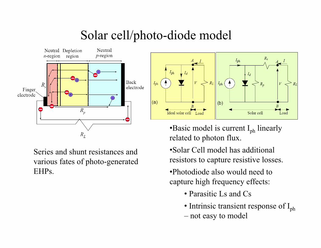
Series and shunt resistances and various fates of photo-generated EHPs.
Solar cell/photo-diode model
• Basic model is current Iph linearly related to photon flux. • Solar Cell model has additional resistors to capture resistive losses. • Photodiode also would need to capture high frequency effects:
• Parasitic Ls and Cs • Intrinsic transient response of Iph – not easy to model
From Principles of Electronic Materials and Devices, Third Edition, S.O. Kasap (© McGraw-Hill, 2005)
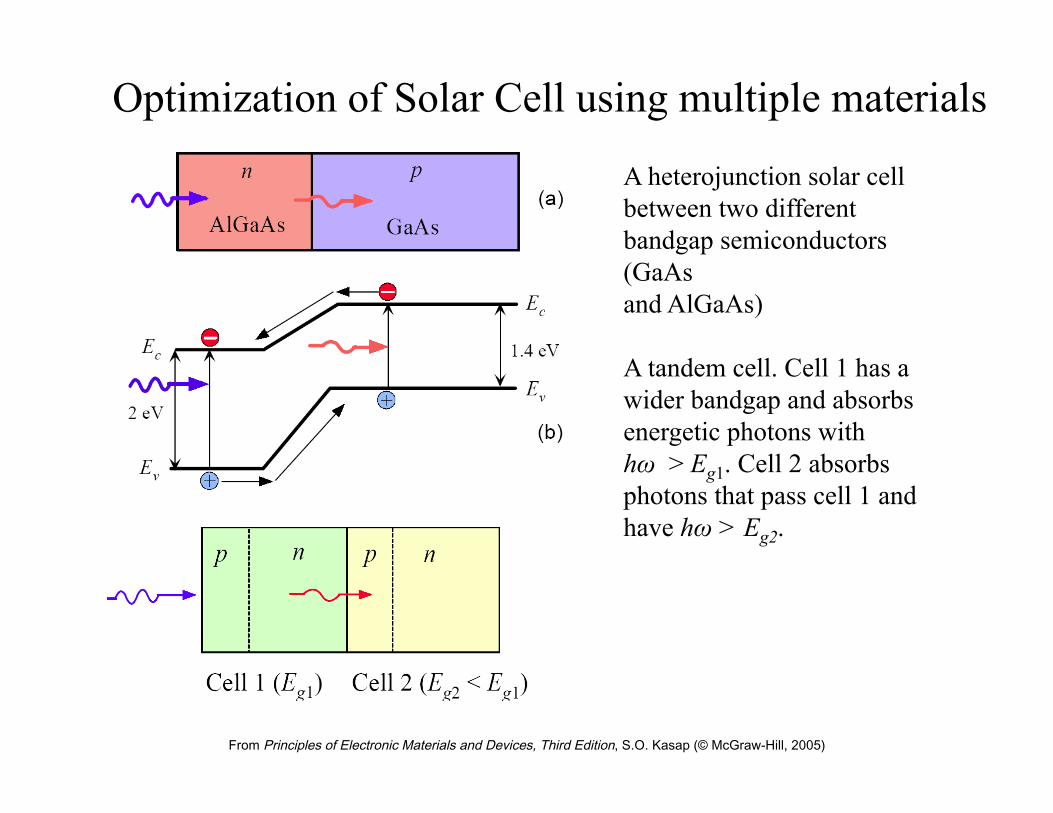
A heterojunction solar cell between two different bandgap semiconductors (GaAs and AlGaAs) A tandem cell. Cell 1 has a wider bandgap and absorbs energetic photons with hω > Eg1. Cell 2 absorbs photons that pass cell 1 and have hω > Eg2.
Optimization of Solar Cell using multiple materials
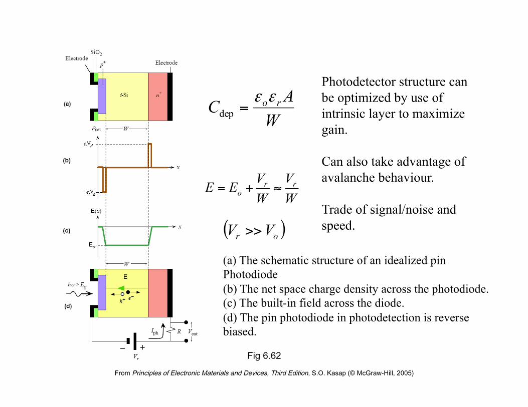
Fig 6.62
From Principles of Electronic Materials and Devices, Third Edition, S.O. Kasap (© McGraw-Hill, 2005)
(a) The schematic structure of an idealized pin Photodiode (b) The net space charge density across the photodiode. (c) The built-in field across the diode. (d) The pin photodiode in photodetection is reverse biased.
WAC roεε=dep
WV
WVEE rr
o ≈+=
( )or VV >>
Photodetector structure can be optimized by use of intrinsic layer to maximize gain. Can also take advantage of avalanche behaviour. Trade of signal/noise and speed.

Fig 6.62
From Principles of Electronic Materials and Devices, Third Edition, S.O. Kasap (© McGraw-Hill, 2005)
Summary