Automotive 12-V to 24-V Engine Load Interface Reference …
36
12 V–24 V Battery Reverse Polarity Protection DC/DC Buck Converter 12/24 V to 6 V 3.3-V LDO MCU Motor Driver Power MOSFET Stages Current Shunt Resistors Current Sense Amplifiers JTAG Push Buttons Status LEDs Output Load A Output Load B Output Load CH Output Load CL 1 TIDUEW6 – April 2020 Submit Documentation Feedback Copyright © 2020, Texas Instruments Incorporated Automotive 12-V to 24-V Engine Load Interface Reference Design Design Guide: TIDA-060030 Automotive 12-V to 24-V Engine Load Interface Reference Design Description This reference design is a 3-phase, ½ H-bridge motor drive with independent FET capability that interfaces with solenoid loads found in gasoline and diesel engine platforms such as automotive solenoids, bidirectional brushed- or brushless-DC motors, unidirectional brushed-DC motors, and relays. The DRV8343-Q1 motor driver is featured on this design and supports up to 6 independent loads per device, with configurability for any architecture of load output configurations. This reference design features 4 distinct outputs to showcase the versatility of the DRV8343-Q1: solenoid with push-pull configuration, solenoid with high-side and low-side gate drivers, and independent high-side and low-side loads. These loads are independently driven using an automotive TMS320F28035 C2000 high-efficiency 32-bit microcontroller. Resources TIDA-060030 Design Folder DRV8343-Q1 Product Folder LMR36006-Q1 Product Folder TPS7B81-Q1 Product Folder TMS320F28035 Product Folder Search Our E2E™ support forums Features • Supports 12-V or 24-V automotive systems • Operating range 5.5-V to 40-V continuous, up to 60-V transient capability • 20-A peak current load driving capability • Controls up to 6 engine loads independently in four different load configurations • Small board size and solution (< 16 sq. in.) • Suite of protection and diagnostic features • AEC-Q100 Grade 1 qualified Applications • 12-V and 24-V automotive motor-control • BLDC and BDC motor modules • Fans and blowers • Fuel and water pumps • Solenoid drive – Gasoline engine – Diesel engine – Gasoline and diesel platform
Transcript of Automotive 12-V to 24-V Engine Load Interface Reference …
12 V±24 V
Battery
Reverse Polarity
Protection
DC/DC Buck
Converter
12/24 V to 6 V
3.3-V LDO
MCU Motor Driver
Power
MOSFET
Stages
Current Shunt
Resistors
Current Sense
Amplifiers
JTAG
Push
Buttons
Status
LEDs
Output Load A
Output Load B
Output Load CH
Output Load CL
1TIDUEW6–April 2020Submit Documentation Feedback
Copyright © 2020, Texas Instruments Incorporated
Automotive 12-V to 24-V Engine Load Interface Reference Design
Design Guide: TIDA-060030Automotive 12-V to 24-V Engine Load Interface ReferenceDesign
DescriptionThis reference design is a 3-phase, ½ H-bridge motordrive with independent FET capability that interfaceswith solenoid loads found in gasoline and dieselengine platforms such as automotive solenoids,bidirectional brushed- or brushless-DC motors,unidirectional brushed-DC motors, and relays. TheDRV8343-Q1 motor driver is featured on this designand supports up to 6 independent loads per device,with configurability for any architecture of load outputconfigurations. This reference design features 4distinct outputs to showcase the versatility of theDRV8343-Q1: solenoid with push-pull configuration,solenoid with high-side and low-side gate drivers, andindependent high-side and low-side loads. Theseloads are independently driven using an automotiveTMS320F28035 C2000 high-efficiency 32-bitmicrocontroller.
Resources
TIDA-060030 Design FolderDRV8343-Q1 Product FolderLMR36006-Q1 Product FolderTPS7B81-Q1 Product FolderTMS320F28035 Product Folder
Search Our E2E™ support forums
Features• Supports 12-V or 24-V automotive systems• Operating range 5.5-V to 40-V continuous, up to
60-V transient capability• 20-A peak current load driving capability• Controls up to 6 engine loads independently in four
different load configurations• Small board size and solution (< 16 sq. in.)• Suite of protection and diagnostic features• AEC-Q100 Grade 1 qualified
Applications• 12-V and 24-V automotive motor-control• BLDC and BDC motor modules• Fans and blowers• Fuel and water pumps• Solenoid drive
– Gasoline engine– Diesel engine– Gasoline and diesel platform

System Description www.ti.com
2 TIDUEW6–April 2020Submit Documentation Feedback
Copyright © 2020, Texas Instruments Incorporated
Automotive 12-V to 24-V Engine Load Interface Reference Design
An IMPORTANT NOTICE at the end of this TI reference design addresses authorized use, intellectual property matters and otherimportant disclaimers and information.
1 System DescriptionThe TIDA-060030 is an example of a system used to drive independent loads for automotive applicationssuch as solenoids, relays, and unidirectional BDC motors. The intent is to drive loads that are found inEngine Control Units (ECUs). Internal Combustion Engines (ICE) will be the largest market for ECUs untilthe emergence of Hybrid Electric Vehicles, and engine platforms can require up to as many as 60 general-purpose outputs. Some examples of possible output loads are starter relays, canister purge valves, andwastegate solenoids. These outputs are often driven thousands of times per second to maintain engineefficiency and performance. The DRV8343-Q1 device is a motor gate driver that can independently driveloads by individually driving the high-side and low-side MOSFETs, allowing up to 6 independent loads(high-side and low-side from each phase) to be driven. The TIDA-060030 is designed so that a variety ofengine loads can be driven from the DRV8343-Q1: phase A drives a unidirectional BDC motor, phase Bdrives a solenoid with high- and low-side drivers, and phase C separates the high-side and low-side loadsto drive two independent solenoids. The reference design is powered from an automotive 12-V or 24-Vbattery and supports a wide input voltage range of 5.5 V–40 V.
Figure 1. TIDA-060030 Top View

www.ti.com System Description
3TIDUEW6–April 2020Submit Documentation Feedback
Copyright © 2020, Texas Instruments Incorporated
Automotive 12-V to 24-V Engine Load Interface Reference Design
1.1 Key System Specifications
Table 1. Key System Specifications
PARAMETER COMMENTS MIN TYP MAX UNITSystem InputVIN Input voltage VBAT input 5.5 12 or 24 40 VVOUT Phase output
voltageVM 5.5 12 or 24 40 V
IIN Input current VBAT input current 0 - 20 AIOUT Output current Should be less than
IIN0 - 20 A
fPWM PWM frequency 15 - 50 kHzVBUCK Buck converter
output voltageLMR36006-Q1output voltage
- 6 - V
IBUCK Buck output current LMR36006-Q1output current
- 600 - mA
VLDO LDO output voltage TPS7B81-Q1 outputvoltage
- 3.3 - V
ILDO LDO output current TPS7B81-Q1 outputcurrent
- 150 - mA
12 V±24 V
Battery
Reverse Polarity
Protection
DC/DC Buck
Converter
12/24 V to 6 V
3.3-V LDO
MCU Motor Driver
Power
MOSFET
Stages
Current Shunt
Resistors
Current Sense
Amplifiers
JTAG
Push
Buttons
Status
LEDs
Output Load A
Output Load B
Output Load CH
Output Load CL
System Overview www.ti.com
4 TIDUEW6–April 2020Submit Documentation Feedback
Copyright © 2020, Texas Instruments Incorporated
Automotive 12-V to 24-V Engine Load Interface Reference Design
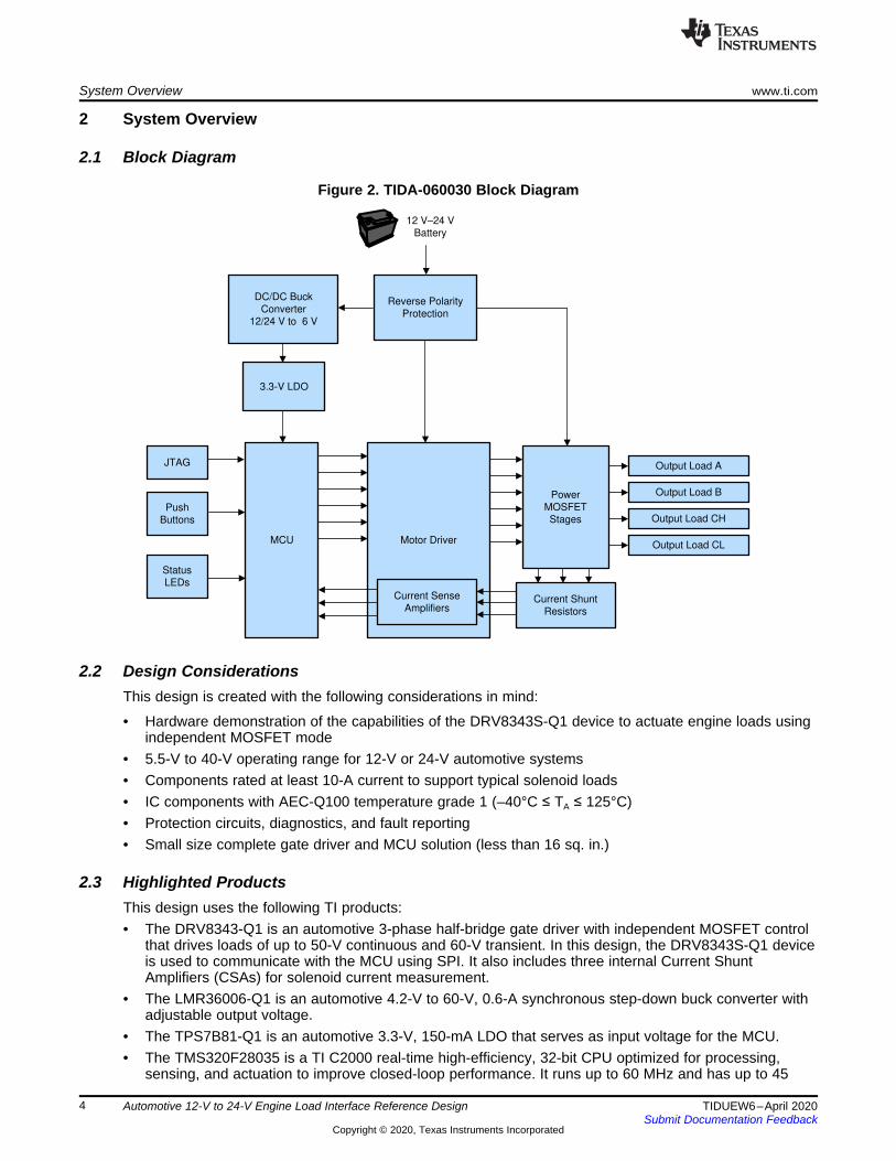
2 System Overview
2.1 Block Diagram
Figure 2. TIDA-060030 Block Diagram
2.2 Design ConsiderationsThis design is created with the following considerations in mind:
• Hardware demonstration of the capabilities of the DRV8343S-Q1 device to actuate engine loads usingindependent MOSFET mode
• 5.5-V to 40-V operating range for 12-V or 24-V automotive systems• Components rated at least 10-A current to support typical solenoid loads• IC components with AEC-Q100 temperature grade 1 (–40°C ≤ TA ≤ 125°C)• Protection circuits, diagnostics, and fault reporting• Small size complete gate driver and MCU solution (less than 16 sq. in.)
2.3 Highlighted ProductsThis design uses the following TI products:• The DRV8343-Q1 is an automotive 3-phase half-bridge gate driver with independent MOSFET control
that drives loads of up to 50-V continuous and 60-V transient. In this design, the DRV8343S-Q1 deviceis used to communicate with the MCU using SPI. It also includes three internal Current ShuntAmplifiers (CSAs) for solenoid current measurement.
• The LMR36006-Q1 is an automotive 4.2-V to 60-V, 0.6-A synchronous step-down buck converter withadjustable output voltage.
• The TPS7B81-Q1 is an automotive 3.3-V, 150-mA LDO that serves as input voltage for the MCU.• The TMS320F28035 is a TI C2000 real-time high-efficiency, 32-bit CPU optimized for processing,
sensing, and actuation to improve closed-loop performance. It runs up to 60 MHz and has up to 45

www.ti.com System Overview
5TIDUEW6–April 2020Submit Documentation Feedback
Copyright © 2020, Texas Instruments Incorporated
Automotive 12-V to 24-V Engine Load Interface Reference Design
programmable GPIO pins, SPI modules, ePWM modules, and ADC modules that are beneficial to thisreference design.
2.3.1 DRV8343S-Q1The DRV8343S-Q1 is an independent half-bridge gate driver with dedicated source (SHx) and drain (DLx)pins to support independent MOSFET control. It supports 5.5-V to 60-V continuous input supply and isintended for 12-V or 24-V automotive systems. It is featured in the TIDA-060030 to demonstrateindependent MOSFET mode and actuate up to 6 solenoid loads quickly and independently. TheDRV8343S-Q1 incorporates an integrated charge pump output to drive reverse polarity detection, includesprotection and diagnostic features, and is AEC-Q100 temperature Grade 1 qualified. Ideally this design isto target ECUs to control relays, valves, brushed-DC motors, and solenoids found inside of gasoline anddiesel engines.
2.3.2 LMR36006-Q1The LMR36006-Q1 is a synchronous, step-down DC/DC converter intended for automotive applications. Itsupports a wide input voltage range of 4.2-V to 60-V and up to 600 mA of output current, includesprotection features such as thermal shutdown, input undervoltage lockout, and short-circuit protection, andis AEC-Q100 temperature Grade 1 qualified. Passive components are selected using TI's WEBENCH®
Power Designer to step supply voltage down to 6-V and give extra headroom voltage to increase LDOefficiency.
2.3.3 TPS7B81-Q1The TPS7B81-Q1 is an automotive low-dropout linear regulator with a wide input voltage range of 3-V to40-V and maximum output current of 150 mA. It steps the 6-V input voltage into a fixed 3.3-V outputvoltage for the TMS320F28035 C2000 MCU. It includes integrated fault protections such as thermalshutdown, short-circuit, and overcurrent protection. It is also AEC-Q100 temperature Grade 1 qualified.
2.3.4 TMS320F28035The TMS320F28035 is a high-efficiency 32-bit CPU that is part of TI's C2000 family. It comes in a 56-pinRSH VQFN package and is AEC-Q100 temperature Grade 1 qualified for automotive applications. TheTMS320F28035 requires a single 3.3-V supply powered from the LDO and has up to 45 individuallyprogrammable, multiplexed GPIO pins. It supports control peripherals such as ePWM, ADC, an on-chiptemperature sensor, and comparators suitable for motor drive applications. It also incorporates serial portcommunication peripherals, including:• One Serial Communications Interface (SCI) Universal Asynchronous Receiver, and Transmitter
(UART) Module• Two Serial Peripheral Interface (SPI) Modules• One Inter-Integrated-Circuit (I2C) Module• One Local Interconnect Network (LIN) Module• One Enhanced Controller Area Network (eCAN) Module

Powerstage & Current Sense
Power Management
Gate Driver
LMR36006-Q1
Step-Down
DC/DC Converter
12±24 V / 6 V
Reverse Polarity
Protection
External MCU
TMS320F28035
C2000 Real-Time
MCU
User Control Inputs
Push Button A
Push Button B
Push Button CH
Push Button CL
Push Button Open
Lead Detect
Output Status LEDs
Output Load LED A
Output Load LED B
Output Load LED C
Output Load LED D
JTAG
Interface
DRV8343S-Q1
Independent Half-Bridge
Gate Driver with SPI
INHA
INLA
INHB
INLB
INHC
INLC
ENABLE
SDO
SDI
SCLK
nSCS
SOA
SOB
SOC
SQJ850EP-T1
Phase A High
Side FET
SQJ850EP-T1
Phase A Low
Side FET
SQJ850EP-T1
Phase B High
Side FET
SQJ850EP-T1
Phase B Low
Side FET
SQJ850EP-T1
Phase C High
Side FET
SQJ850EP-T1
Phase C Low
Side FET
Current
Sense
ACurrent
Sense
B Current
Sense
C
Output Load
Phase B
Solenoid with
HS-/LS- Drivers
Output Load
Phase CH
Solenoid
with HS-Driver
12 V±24 V
Battery
VM
Output Load
Phase A
Unidirectional
Brushed-DC
Motor
VM
Output Load
Phase CH
Solenoid
with HS- driver
VCP
DVDD
GND
GND
VMTPS7B81-Q1
Low-Dropout
3.3-V Linear
Regulator
GND GND GND
Current Sense
Amplifiers (CSAs)
System Overview www.ti.com
6 TIDUEW6–April 2020Submit Documentation Feedback
Copyright © 2020, Texas Instruments Incorporated
Automotive 12-V to 24-V Engine Load Interface Reference Design
2.4 System Design Theory
Figure 3. TIDA-060030 Detailed Block Diagram
2.4.1 Printed Circuit Board (PCB) and Form Factor• Compatible with C2000 MCU, programmable with JTAG interface• Optimized size for potential in-application use• Sufficient size for high current and thermal dissipation• Organized layout to demonstrate PCB flow

www.ti.com System Overview
7TIDUEW6–April 2020Submit Documentation Feedback
Copyright © 2020, Texas Instruments Incorporated
Automotive 12-V to 24-V Engine Load Interface Reference Design
Figure 4. TIDA-060030 PCB Render
2.4.2 Overall Considerations for Component SelectionComponents selected are based on the performance requirements of the expected applications. The mainpriority for component selection is automotive qualification using AEC-Q100 active components, AEC-Q101 discrete components, and AEC-Q200 passive components.
Capacitors are X7R grade (−55°C to +125°C) or higher, with size and value selected for the expectedextremes of operation conditions. The voltage rating of the capacitors should be greater than themaximum voltage they could experience, and 2 × the typical operating voltage to avoid DC bias effects.The amount of output capacitance used depends on output ripple and transient response requirements,and many equations and tools are available online to help estimate these values.
For improved accuracy, feedback resistor dividers should use components with 1% or better tolerance.Resistance tolerance in this design was selected to reduce the total amount of BOM line items. In thedesign considerations, it is noted where 5% or 10% precision resistors can be used to reduce the cost of aspecific individual resistor. Using less precise resistors for cost reasons should be weighed againstreducing the amount of BOM line items and ordering in higher volumes to reduce total BOM cost.
Zero-Ohm (0-Ω) resistors are used at the input and output of several of the circuit sections for testingpurposes only, and could be removed, if needed, in a production board design.

PGND1
VIN2
NC3
BST4
VCC5
AGND6
FB7
PG8
EN9
VIN10
PGND11
SW12
LMR36006AQRNXRQ1
U2
100V4.7uF
C2822nF100V
C2422nF100V
C21
100V1uF
C19
GND
25V100pF
C20
16V22uF
C17
47uH
L1
100kR18
20.0kR17
VM
6V_BUCK
VCC FB
SW
BST
VBAT
GND
1uFC45
0.01uFC48
GND
1uHL2 VM
GND
0.1uFC46
1000pFC49
GND
VCP
10k
R43
10kR38
VM1
1
2
H6
330uFC37
0.01uFC32
1000pFC33
0.1uFC31
1uFC29
93.1kR31
4.99kR32
0.1uFC42
GND
VSEN_VM
3
1
2 Q8
5
4
1
2
3
Q7
D12
CD0603-S0180
System Overview www.ti.com
8 TIDUEW6–April 2020Submit Documentation Feedback
Copyright © 2020, Texas Instruments Incorporated
Automotive 12-V to 24-V Engine Load Interface Reference Design
2.5 Power Management
2.5.1 VBAT Input Protection and Pi FilterReverse battery protection is required in nearly every electronic subsystem of a vehicle, both by OEMstandards, as well as ISO 16750-2, an international standard pertaining to supply quality.
This implementation uses a power NMOS and an NPN bipolar junction transistor (BJT) to achieve reversebattery protection. If the battery is connected in reverse, the body diode of the NMOS will not conductcurrent nor turn the NMOS on, thereby protecting the system from the reverse polarity condition. When thebattery is connected correctly, the circuit permits current to flow with very little power lost because of thelow RDS(on) of the NMOS.
This technique is particularly well-suited for motor drive applications. The DRV8343S-Q1 includesintegrated charge pump devices, which can support the required overdrive voltage for the NMOS gatewithout the need for additional external circuitry. For more background information on reverse polarityprotection, see the Protecting automotive motor-drive systems from reverse polarity conditions applicationreport.
After passing the reverse polarity circuit, the power supply uses a set of capacitors and inductors to form a“pi” filter. This removes unwanted AC components on the supply line. Due to the bidirectional format of thepi filter, incoming transients are blocked from entering the board, and any switching noise or clock noisegenerated on the board is blocked from propagating into the rest of the voltage.
Figure 5. Reverse Polarity Protection for VBAT and Pi Filter
2.5.2 Buck ConverterThe TIDA-060030 uses an LMR36006-Q1 synchronous, step-down buck converter to step down the inputsupply voltage to a 6-V signal. This buck converter is designed for automotive applications and is AEC-Q100 temperate Grade 1 qualified. After stepping down the input supply voltage, that signal is input intothe LDO stage to provide high efficiency and minimal power losses.
Figure 6. LMR36006-Q1 Automotive Buck Converter to Step 24-V Down to 6-V

3.3V_LDO26V_BUCK
GND
GND
GND
22uF
C15
22uF
C18
1
IN1
EN2
GND4
DNC5
PAD7
OUT6
GND3
TPS7B8133QDRVRQ1
U1
www.ti.com System Overview
9TIDUEW6–April 2020Submit Documentation Feedback
Copyright © 2020, Texas Instruments Incorporated
Automotive 12-V to 24-V Engine Load Interface Reference Design
For buck external component selection, Texas Instruments' WEBENCH® Power Designer specifies thecorrect values based on user input specifications. The tool is found on the LMR36006-Q1 product page onTI.com. A WEBENCH simulation was run for the maximum input voltage the tool allowed (8 V–40 V), 0.6-A max current, and ambient temperature.
Figure 7. WEBENCH® Power Designer Tool for LMR36006-Q1
2.5.3 3.3-V Linear Dropout RegulatorThe 6-V signal is fed into the TPS7B81-Q1 to provide the 3.3-V supply needed to bias the TMS320F28035MCU and logic-level components. The TPS7B81-Q1 is a small, efficient solution intended for automotiveapplications. It has a maximum output current of 150 mA and operates over a wide junction temperaturerange of –40°C to 150°C. It also has low quiescent current IQ of 300 nA to conserve energy and extendbattery lifetime. TI recommends using a low-equivalent series resistance (ESR) ceramic capacitor with anX5R- or X7R-type dielectric. In the TIDA-060030, 22-µF ceramic capacitors are used for the input andoutput to counteract reactive input sources and improve transient response, input ripple rejection, andPSRR.
Figure 8. TPS7B81-Q1 3.3-V Automotive LDO
2.6 MicrocontrollerThe TMS320F28035 serves as the external MCU for the TIDA-060030 design to receive pushbuttoninputs, send input signals to the gate driver, set fault configurations, diagnose faults, and calculate voltageand current feedback from the phase nodes. An SPI is used to set configurations and receive faultdiagnostics with the DRV8343S-Q1. ePWM modules are used to receive control signals from thepushbutton inputs, and general purpose I/O pins send the logic-level signals to the motor driver and statusLEDs. The ADC modules convert voltages from the phase nodes and SOx pins to respectively translatevoltages and currents from the system.
GPIO22/EQEP1S/LINTXA1
GPIO23/EQEP1I/LINRXA2
XRS5
TRST6
ADCINA77
ADCINA6/COMP3A/AIO68
ADCINA4/COMP2A/AIO49
ADCINA310
ADCINA2/COMP1A/AIO211
ADCINA112
ADCINA0/VREFHI13
ADCINB116
ADCINB2/COMP1B/AIO1017
ADCINB318
ADCINB4/COMP2B/AIO1219
ADCINB6/COMP3B/AIO1420
ADCINB721
GPIO31/CANTXA22
GPIO30/CANRXA23
TEST227
GPIO28/SCIRXDA/SDAA/TZ228
GPIO18/SPICLKA/LINTXA/XCLKOUT29
GPIO17/SPISOMIA/TZ330
GPIO16/SPISIMOA/TZ231
GPIO12/TZ1/SCITXDA32
GPIO7/EPWM4B/SCIRXDA33
GPIO6/EPWM4A/EPWMSYNCI/EPWMSYNCO34
X235
X136
GPIO19/XCLKIN/SPISTEA/LINRXA/ECAP139
GPIO38/TCK/XCLKIN40
GPIO37/TDO41
GPIO35/TDI42
GPIO36/TMS43
GPIO5/EPWM3B/SPSIMOA/ECAP144
GPIO4/EPWM3A45
GPIO3/EPWM2B/SPISOMIA/COMP2OUT46
GPIO2/EPWM2A47
GPIO1/EPWM1B/COMP1OUT48
GPIO0/EPWM1A49
VREGENZ53
GPIO34/COMP2OUT/COMP3OUT54
GPIO20/EQEP1A/COMP1OUT55
GPIO21/EQEP1B/COMP2OUT56
GPIO29/SCITXDA/SCLA/TZ324
TMS320F28035RSHS
U4A
TRST
GND
TDITMSTDOTCK
SDISDOSCKnSCS
INH_AINL_AINH_BINL_BINH_CINL_C
PB_APB_B
PB_CHPB_CL
ENABLEnFAULT
STATUS_ASTATUS_B
STATUS_CHSTATUS_CL
VSEN_CH
VSEN_A
VSEN_B
VSEN_VM
ISEN_A
ISEN_B
ISEN_C
AI1
AI2
AI3
POT
nRESET
VSEN_CL
STATUS_MCU1
STAT US_MCU2
0
R36
OL
System Overview www.ti.com
10 TIDUEW6–April 2020Submit Documentation Feedback
Copyright © 2020, Texas Instruments Incorporated
Automotive 12-V to 24-V Engine Load Interface Reference Design
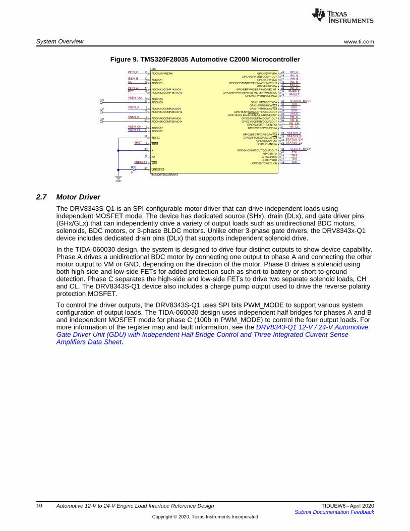
Figure 9. TMS320F28035 Automotive C2000 Microcontroller
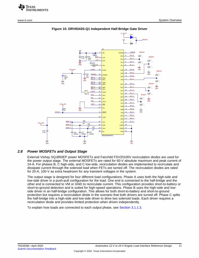
2.7 Motor DriverThe DRV8343S-Q1 is an SPI-configurable motor driver that can drive independent loads usingindependent MOSFET mode. The device has dedicated source (SHx), drain (DLx), and gate driver pins(GHx/GLx) that can independently drive a variety of output loads such as unidirectional BDC motors,solenoids, BDC motors, or 3-phase BLDC motors. Unlike other 3-phase gate drivers, the DRV8343x-Q1device includes dedicated drain pins (DLx) that supports independent solenoid drive.
In the TIDA-060030 design, the system is designed to drive four distinct outputs to show device capability.Phase A drives a unidirectional BDC motor by connecting one output to phase A and connecting the othermotor output to VM or GND, depending on the direction of the motor. Phase B drives a solenoid usingboth high-side and low-side FETs for added protection such as short-to-battery or short-to-grounddetection. Phase C separates the high-side and low-side FETs to drive two separate solenoid loads, CHand CL. The DRV8343S-Q1 device also includes a charge pump output used to drive the reverse polarityprotection MOSFET.
To control the driver outputs, the DRV8343S-Q1 uses SPI bits PWM_MODE to support various systemconfiguration of output loads. The TIDA-060030 design uses independent half bridges for phases A and Band independent MOSFET mode for phase C (100b in PWM_MODE) to control the four output loads. Formore information of the register map and fault information, see the DRV8343-Q1 12-V / 24-V AutomotiveGate Driver Unit (GDU) with Independent Half Bridge Control and Three Integrated Current SenseAmplifiers Data Sheet.
AGND38
CAL37
CPH2
CPL1
DVDD39
ENABLE36
SCS35
GHA6
SLB15
GLB16
GLA9
SNB13
SHB18
SDI33
INHA41
INHB43
INHC45
INLA42
INLB44
INLC46
SDO32
PAD49
PGND47
SHA7
SPB14
DLB17
SLA10
SPA11
GHC20
GLC23
DLC22
SHC21
DLA8
SNA12
GHB19
VCP3
VDRAIN5
SCLK34
VM4
VREF30
FAULT31
SLC24
SPC25
SNC26
SOC27
SOB28
SOA29
NC48
VSDO40
U3
DRV8343SPHPQ1
GND
GH_A
SH_A
GL_A
DL_A
GH_B
SH_B
GL_B
DL_B
GH_C
SH_C
GL_C
DL_C
SP_C
SN_C
SL_C
SP_B
SN_B
SL_B
SP_A
SN_A
SL_A
ISEN_A
ISEN_B
ISEN_C
INL_CINH_C
INL_BINH_B
INL_AINH_A
ENABLE
VM
GND
4.7uFC38
GND
VDRAIN
3.3V_LDO
0.1uFC34
GND
10kR28
3.3V_LDO
GND
nFAULT
DVDD
VCP
2200pF
C30
2200pFC27
GND
SDO
SDI
SCK
nSCS
2200pFC23
56
R24
56
R25
56
R27
D166V_BUCK
3.3V_LDO
GND
1µFC35
100nF100V
C36
47nF100V
C39
100nF16V
C41 1µF6.3V
C40
VSDO
CPH
CPL
NT17
Net-Tie
RESDIV
GND
GND
GND
GND
GND
D15
DNP
VM
RESDIV
RESDIV
RESDIV
RESDIV
RESDIV
47.0kR60
DNP
47.0kR61
DNP47.0kR54
DNP
47.0kR56
DNP
47.0kR55
DNP
47.0kR57
DNP
47.0kR53
DNP
47.0kR52
DNP
47.0kR59
DNP
47.0kR58
DNP
www.ti.com System Overview
11TIDUEW6–April 2020Submit Documentation Feedback
Copyright © 2020, Texas Instruments Incorporated
Automotive 12-V to 24-V Engine Load Interface Reference Design
Figure 10. DRV8343S-Q1 Independent Half-Bridge Gate Driver
2.8 Power MOSFETs and Output StageExternal Vishay SQJ850EP power MOSFETs and Fairchild FSV20100V recirculation diodes are used forthe power output stage. The external MOSFETs are rated for 60-V absolute maximum and peak current of24-A. For phases B, C high-side, and C low-side, recirculation diodes are implemented to recirculate anddissipate current through the solenoid load when FETs are turned off. The recirculation diodes are ratedfor 20-A, 100-V as extra headroom for any transient voltages in the system.
The output stage is designed for four different load configurations. Phase A uses both the high-side andlow-side driver in a push-pull configuration for the load. One end is connected to the half-bridge and theother end is connected to VM or GND to recirculate current. This configuration provides short-to-battery orshort-to-ground detection and is suited for high-speed operations. Phase B uses the high-side and low-side driver in an half-bridge configuration. This allows for both short-to-battery and short-to-groundprotection but requires a recirculation diode in the scenario that both drivers are turned off. Phase C splitsthe half-bridge into a high-side and low-side driver to drive two solenoid loads. Each driver requires arecirculation diode and provides limited protection when driven independently.
To explain how loads are connected to each output phase, see Section 3.1.1.3.

VM
GH_A
GL_A
0
R29
0
R26
SH_ANT15
Net-Tie
NT14
Net-Tie
SL_A
NT5
Net-Tie
NT6
Net-Tie
0.01uFC4
0.01uFC3
SP_A
SN_A
1000pFC26
VM
GH_B
GL_B
0
R23
0
R20
SH_BNT9
Net-Tie
GND
NT12
Net-Tie
SL_B
NT1
Net-Tie
NT3
Net-Tie
SP_B
SN_B
0.01uFC1
0.01uFC6
1000pFC22
VM
GH_C
GL_C
0
R21
0
R22
SH_CNT11
Net-Tie
GND
NT13
Net-Tie
SL_C
NT2
Net-Tie
NT4
Net-Tie
0.01uFC2
0.01uFC5
SP_C
SN_C
DL_ANT16
Net-Tie
DL_BNT8
Net-Tie
DL_CNT10
Net-Tie
GND
GND
OUT_A1
VM
OU
T_
C2
OUT_C1
OUT_C2
GND
OU
T_
C1
GND
GND
OUT_B1
OUT_B2
NT7VDRAIN
1000pFC25
100R2
100R1100
R4
100R12
100R13
100R8
1uF
C8
1uF
C12
1uF
C1610nFC7
10nFC13
10nFC14
330uFC11
330uFC9
330uFC10
1
3
2
D1FSV20100V
0.005R11
0.005R6 0.005
R7
1
3
2
D13FSV20100V
1
3
2
D14FSV20100V
4
25
1 3
Q4
SQJ850EP-T1-GE3
4
25
1 3
Q3
SQJ850EP-T1-GE3
4
25
1 3
Q1
SQJ850EP-T1-GE3
4
25
1 3
Q6
SQJ850EP-T1-GE34
25
1 3
Q5
SQJ850EP-T1-GE3
4
25
1 3
Q2
SQJ850EP-T1-GE3
Unidirectional BDCMotor
Solenoid Load -Recirculation diode
needed in parallel withw/ solenoid
HS / LS LoadsRecirculation diodesneeded on each load
System Overview www.ti.com
12 TIDUEW6–April 2020Submit Documentation Feedback
Copyright © 2020, Texas Instruments Incorporated
Automotive 12-V to 24-V Engine Load Interface Reference Design
Figure 11. TIDA-060030 Power Stage for Phases A, B, C High-Side, and C Low-Side
2.9 Current FeedbackExternal shunt resistors are used to measure the current going through the phase node. The SPx and SNxpins measure the high- and low-side voltages of the resistor. Those voltages are fed to the Current SenseAmplifiers (CSAs) integrated in the DRV8343S-Q1 to calculate the sense current of that phase through theshunt resistor. That current is sent as a voltage through its respective SOx pin back to the TMS320F28035device, which is read by an ADC pin.
Because the large currents in the power stage flow through the sense resistor, the selected resistor valuemust be small to keep the power dissipation at a minimum. For high current systems, the resistor value isusually in mΩ. In the TIDA-060030 design, up to 20 A of current can sink through the 5-mΩ sense resistorR11. This dissipates 2 W of power through that resistor. Increasing the resistor value can improve thesignal-to-noise ratio but will also increase the power dissipation.
One important factor to consider is that current cannot be measured through the high-side FET of phaseC. This is because shunt resistors need to be placed near ground, and CH does not have any connectionsto ground.
Figure 12. Current Sense Voltages From the SOx Pins of theDRV8343-Q1 to the MCU
Figure 13. Voltages SPx and SNx Across the Current ShuntResistor are fed to the Internal Current Sense Amplifier (CSA)

OUT_A1 OUT_B1
OUT_C2
GND
93.1kR5
4.99kR45
GND
VSEN_A
93.1kR10
4.99kR46
GND
VSEN_B
93.1kR9
4.99kR47
GND
VSEN_CH
OUT_C1
0.1uF
C53
0.1uF
C54
0.1uF
C55
1
2
H1
1
2
H2
1
2
3
H5
VM
4.99kR44
93.1kR3
GND
VSEN_CL
0.1uF
C52
OUT_C2
OUT_B2
www.ti.com System Overview
13TIDUEW6–April 2020Submit Documentation Feedback
Copyright © 2020, Texas Instruments Incorporated
Automotive 12-V to 24-V Engine Load Interface Reference Design
2.10 Voltage FeedbackA resistor divider is used to step down the output and supply voltages to logic-level voltages read by theADC module of the TMS320F28035. The same voltage divider circuit is used on all output loads: phase A,B, C high-side, and C low-side. In the TIDA-060030, the resistor values used for the voltage divider are93.1 kΩ for the high resistor and 4.99 kΩ for the low resistor. These values are specifically chosen to stepdown a full-load output voltage signal to a full-scale ADC logic-level signal.
It is imperative that these resistors are precise with 1% or better tolerance to obtain accuratemeasurements of feedback voltage.
Figure 14. Voltage Feedback for VM, Phase A, Phase B, Phase CH, and Phase CL
Hardware, Software, Testing Requirements, and Test Results www.ti.com
14 TIDUEW6–April 2020Submit Documentation Feedback
Copyright © 2020, Texas Instruments Incorporated
Automotive 12-V to 24-V Engine Load Interface Reference Design
3 Hardware, Software, Testing Requirements, and Test Results
3.1 Required Hardware and Software
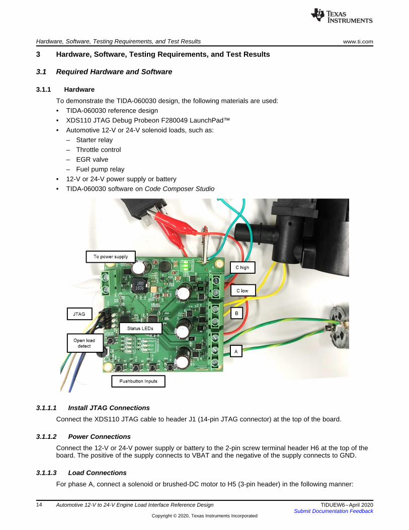
3.1.1 HardwareTo demonstrate the TIDA-060030 design, the following materials are used:• TIDA-060030 reference design• XDS110 JTAG Debug Probeon F280049 LaunchPad™• Automotive 12-V or 24-V solenoid loads, such as:
– Starter relay– Throttle control– EGR valve– Fuel pump relay
• 12-V or 24-V power supply or battery• TIDA-060030 software on Code Composer Studio
3.1.1.1 Install JTAG ConnectionsConnect the XDS110 JTAG cable to header J1 (14-pin JTAG connector) at the top of the board.
3.1.1.2 Power ConnectionsConnect the 12-V or 24-V power supply or battery to the 2-pin screw terminal header H6 at the top of theboard. The positive of the supply connects to VBAT and the negative of the supply connects to GND.
3.1.1.3 Load ConnectionsFor phase A, connect a solenoid or brushed-DC motor to H5 (3-pin header) in the following manner:

www.ti.com Hardware, Software, Testing Requirements, and Test Results
15TIDUEW6–April 2020Submit Documentation Feedback
Copyright © 2020, Texas Instruments Incorporated
Automotive 12-V to 24-V Engine Load Interface Reference Design
• Connect the positive or high-side terminal of the motor to the OUT_A screw terminal• Connect the negative or low-side terminal of the motor to the GND or VM screw terminal, depending
on the push-pull configuration of the solenoid or direction of the brushed-DC motor
For Phase B, connect a solenoid to H1 (2-pin header) to the OUT_BH and OUT_BL screw terminals.
For phase C, connect a solenoid load using one of the following high- or low-side drivers:• C high-side: Connect one end of the solenoid to the OUT_CH screw terminal, and the other end of the
solenoid to GND• C low-side: Connect one end of the solenoid to VM and connect the other end of the solenoid to the
OUT_CL screw terminal.
3.1.2 Software
3.1.2.1 Download and Install Code Composer Studio™Code Composer Studio is an integrated development environment (IDE) for Texas Instruments (TI)embedded processor families. Code Composer Studio comprises a suite of tools used to develop anddebug embedded applications. It includes compilers for each of TI's device families, source code editor,project build environment, debugger, profiler, simulators, real-time operating system and many otherfeatures. The intuitive IDE provides a single user interface taking you through each step of the applicationdevelopment flow. Familiar tools and interfaces allow users to get started faster than ever before and addfunctionality to their application thanks to sophisticated productivity tools. See the Code Composer Studioweb page at for information on downloading the integrated development environment for the C2000 code.
Software examples for SPI communication, ePWM peripheral setup, I/O setup, ADC module setup, andmore are found in C2000Ware to minimize development time. It includes device-specific drivers, libraries,and peripheral examples for the TMS320F28035.

Hardware, Software, Testing Requirements, and Test Results www.ti.com
16 TIDUEW6–April 2020Submit Documentation Feedback
Copyright © 2020, Texas Instruments Incorporated
Automotive 12-V to 24-V Engine Load Interface Reference Design
3.2 Testing and Results
3.2.1 Test SetupIn the following test setup, the four output loads connected to phases A, B, C high-side, and C low-sideare a brushed-DC motor, canister purge valve, wastegate solenoid, and fuel pump relay. All of thesesolenoids are rated for 12-V and are typically found as driver outputs in a 12-V gasoline or diesel enginesystem.
Specifically, the Brushed-DC motor is connected to OUT_A and VM, the canister purge valve connectedto OUT_BH and OUT_BL, wastegate solenoid connected to OUT_CH and GND, and fuel pump relayconnected to OUT_CL and VM. When their respective push button is pressed down, each output load willactuate independently and its corresponding LED will light up in the "Status LEDs" section of the PCB.
Figure 15 is an illustration of the TIDA-060030 test setup with a brushed-DC motor connected to OUT_Aand VM, canister purge valve connected to OUT_BH and OUT_BL, wastegate solenoid connected toOUT_CH and GND, and fuel pump relay connected to OUT_CL and VM.
Figure 15. TIDA-060030 Test Setup
3.2.2 Test Results
3.2.2.1 Solenoid OperationWhen the TIDA-060030 is powered through VBAT and launched with software, the solenoid loadsconnected to OUT_A, OUT_B, OUT_CH, and OUT_CL can be controlled with pushbuttons OUT_A,OUT_B, OUT_CH, and OUT_CL. LEDs D8–D11 (labeled A, B, CH, and CL) will also light up when buttonsare pressed.
The oscilloscope screenshot in Figure 16 shows the output of PB_A and OUT_A once pushbutton A ispressed.

www.ti.com Hardware, Software, Testing Requirements, and Test Results
17TIDUEW6–April 2020Submit Documentation Feedback
Copyright © 2020, Texas Instruments Incorporated
Automotive 12-V to 24-V Engine Load Interface Reference Design
Figure 16. Plot of PB_A and OUT_A (Brushed-DC Motor) Figure 17. LED for Phase A is on When PB_A is Pressed(Brushed-DC Motor)
3.2.2.2 Power SuppliesEach solenoid load can be controlled independently and simultaneously, resulting in a summation ofoutput currents for each phase. Table 2 shows the progression of output current summation by drivingoutput loads A, B, C, and CH on top of each other and driving with fixed duty cycles for each phase.
Table 2. TIDA-060030 Output Load Current Summation Testing
OUTPUT PHASES LOAD TOTAL OUTPUTCURRENT (A)
A Brushed-DC motor 0.214CL 12-V fuel pump relay 0.121B 12-V canister purge valve 0.363CH 12-V waste gate solenoid 0.169A + B Brushed-DC motor, 12-V fuel pump relay 0.341A + B + CH Brushed-DC motor, 12-V fuel pump relay, 12-V canister
purge valve0.710
A + B + CH + CL Brushed-DC motor, 12-V fuel pump relay, 12-V canisterpurge valve, 12-V waste gate solenoid
0.878
3.2.2.3 Diagnostics and ProtectionIf a fault is generated during device operation, the nFAULT red LED will turn on as well as set the bit ofthe generated fault. Table 3 lists the register map corresponding to the FAULT Status Register. Each faultbit can be read directly from the "Expressions" window during run-time on Code Composer Studio byaddress of the fault bit according to the register map.
Table 3. SPI Register Map for Faults and Diagnostics of DRV8343S-Q1
REGISTERNAME
7 6 5 4 3 2 1 0 Address
FAULTStatus
FAULT GDF CPUV UVLO OCP OTW OTSD OL_SHT 0x00
DIAGStatus A
SA_OC SHT_GND_A
SHT_BAT_A
OL_PH_A VGS_LA VGS_HA VDS_LA VDS_HA 0x01
DIAGStatus B
SB_OC SHT_GND_B
SHT_BAT_B
OL_PH_B VGS_LB VGS_HB VDS_LB VDS_HB 0x02

Hardware, Software, Testing Requirements, and Test Results www.ti.com
18 TIDUEW6–April 2020Submit Documentation Feedback
Copyright © 2020, Texas Instruments Incorporated
Automotive 12-V to 24-V Engine Load Interface Reference Design
Table 3. SPI Register Map for Faults and Diagnostics of DRV8343S-Q1 (continued)REGISTERNAME
7 6 5 4 3 2 1 0 Address
DIAGStatus C
SC_OC SHT_GND_C
SHT_BAT_C
OL_PH_C VGS_LC VGS_HC VDS_LC VDS_HC 0x03
An Open Load Passive (OLP) detection test is initiated by pressing the "Open Load Detect" pushbutton.Software is programmed to run an OLP test by writing a "1" to the EN_OLP bit in address 0x05. If an openload is detected on a phase, the nFAULT LED will light up and the correct fault can be read by reading theDIAG Status A, DIAG Status B, or DIAG Status C registers. Likewise, a short-to-battery or short-to-groundtest is initiated by writing a "1" to the EN_SHT_TST bit in address 0x05. If an short-to-battery or short-to-ground is detected on a phase, the nFAULT LED will light up and the correct fault can be read by readingthe DIAG Status A, DIAG Status B, or DIAG Status C registers.
Many other faults such as gate driver faults (GDF), overcurrent protection (OCP), undervoltage (UVLO),and overtemperature (OTW / OTSD) can be monitored through SPI configuration. For more information ofthe SPI register map and fault information, see the DRV8343-Q1 12-V / 24-V Automotive Gate Driver Unit(GDU) with Independent Half Bridge Control and Three Integrated Current Sense Amplifiers Data Sheet.
Table 4 shows the protection features and diagnostics tested on the TIDA-060030 design.
Table 4. TIDA-060030 Protection Features and Diagnostics Responses
DIAGNOSTIC TEST CONDITIONS VM (V) RESPONSEUndervoltage - < 6 UVLO = 1, nFAULT onOpen load on phase A Phase A disconnected 12 OL_PH_A = 1, OL_SHT = 1, nFAULT on
24Open load on phase B Phase B disconnected 12 OL_PH_B = 1, OL_SHT = 1, nFAULT on
24Open load on phase C Phase C disconnected 12 OL_PH_C = 1, OL_SHT = 1, nFAULT on
24Short to ground on phase A OUT_A connected to GND 12 SHT_GND_A = 1, OL_SHT = 1, nFAULT
on24Short to ground on phase B OUT_B connected to GND 12 SHT_GND_B = 1, OL_SHT = 1, nFAULT
on24Short to ground on phase C OUT_C connected to GND 12 SHT_GND_C = 1, OL_SHT = 1, nFAULT
on24Short to battery on phase A OUT_A connected to VM 12 SHT_BAT_A = 1, OL_SHT = 1, nFAULT on
24Short to battery on phase B OUT_B connected to VM 12 SHT_BAT_B = 1, OL_SHT = 1, nFAULT on
24Short to battery on phase C OUT_C connected to VM 12 SHT_BAT_C = 1, OL_SHT = 1, nFAULT
on24

www.ti.com Design Files
19TIDUEW6–April 2020Submit Documentation Feedback
Copyright © 2020, Texas Instruments Incorporated
Automotive 12-V to 24-V Engine Load Interface Reference Design
4 Design Files
4.1 Altium FilesTo download the Altium Designer® project files, see the design files at TIDA-060030.
4.1.1 SchematicsTo download the schematics, see the design files at TIDA-060030.
4.1.2 Bill of MaterialsTo download the bill of materials (BOM), see the design files at TIDA-060030.
4.1.3 PCB Layout RecommendationsThe PCB design of motor drive systems is non-trivial and requires special considerations and techniquesto achieve the best performance. Power efficiency, high-speed switching frequency, low-noise jitter, andcompact board design are a few primary factors that designers must consider when laying out a motordrive system. Texas Instruments' DRV devices are ideal for such type of systems because they are highlyintegrated and well-equipped with protection circuitry. A major goal of this layout is to highlight the primaryfactors of a motor drive layout when using a DRV device and provide a best practice guideline for a high-performance solution that reduces thermal stress, optimizes efficiency, and minimizes noise in a motordrive application. The TIDA-060030 is a 4-layer board with TOP, POWER, GND, BOTTOM layers.
4.1.3.1 Layout PrintsTo download the layer plots, see the design files at TIDA-060030.
4.1.3.2 Grounding OptimizationA ground plane is used to provide a strong ground return path. Having a continuous ground plane allowssignals to have the shortest return path and decrease coupling and interference. It is imperative tominimize ground discontinuity by carefully routing traces and placing vias in such a manner that it does notcause breaks on the GND plane.

Design Files www.ti.com
20 TIDUEW6–April 2020Submit Documentation Feedback
Copyright © 2020, Texas Instruments Incorporated
Automotive 12-V to 24-V Engine Load Interface Reference Design
Figure 18. GND Plane of TIDA-060030
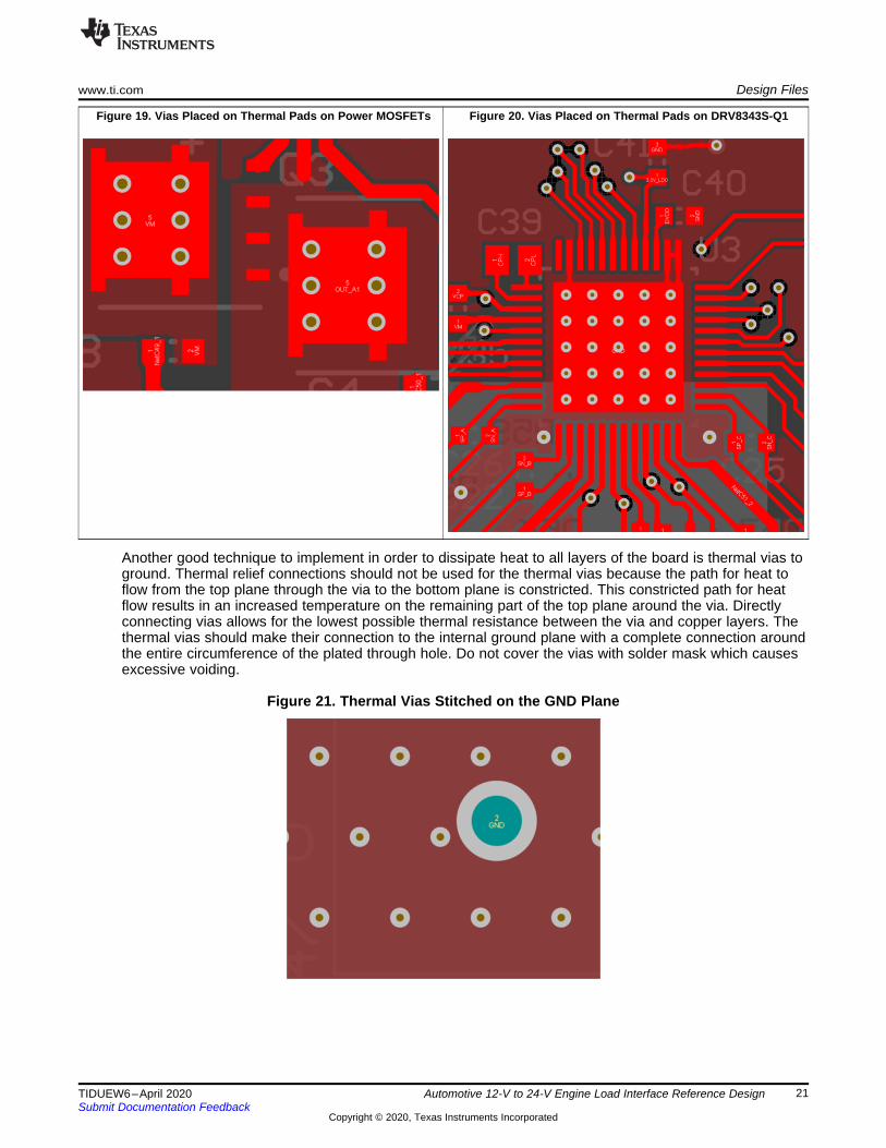
4.1.3.3 Thermal OverviewA thermal pad allows for efficient heat dissipation over a larger area away from important signals andcomponents. The thermal pad should be directly underneath any devices that build up large amounts ofheat, current, or both. In the TIDA-060030 design, vias are placed on the thermal pads of the followingdevices:• DRV8343S-Q1• Vishay external FETs• TMS320F28035
www.ti.com Design Files
21TIDUEW6–April 2020Submit Documentation Feedback
Copyright © 2020, Texas Instruments Incorporated
Automotive 12-V to 24-V Engine Load Interface Reference Design
Figure 19. Vias Placed on Thermal Pads on Power MOSFETs Figure 20. Vias Placed on Thermal Pads on DRV8343S-Q1
Another good technique to implement in order to dissipate heat to all layers of the board is thermal vias toground. Thermal relief connections should not be used for the thermal vias because the path for heat toflow from the top plane through the via to the bottom plane is constricted. This constricted path for heatflow results in an increased temperature on the remaining part of the top plane around the via. Directlyconnecting vias allows for the lowest possible thermal resistance between the via and copper layers. Thethermal vias should make their connection to the internal ground plane with a complete connection aroundthe entire circumference of the plated through hole. Do not cover the vias with solder mask which causesexcessive voiding.
Figure 21. Thermal Vias Stitched on the GND Plane
Design Files www.ti.com
22 TIDUEW6–April 2020Submit Documentation Feedback
Copyright © 2020, Texas Instruments Incorporated
Automotive 12-V to 24-V Engine Load Interface Reference Design
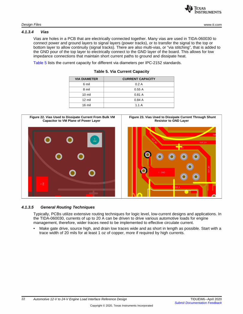
4.1.3.4 ViasVias are holes in a PCB that are electrically connected together. Many vias are used in TIDA-060030 toconnect power and ground layers to signal layers (power tracks), or to transfer the signal to the top orbottom layer to allow continuity (signal tracks). There are also multi-vias, or “via stitching”, that is added tothe GND pour of the top layer to electrically connect to the GND layer of the board. This allows for lowimpedance connections that maintain short current paths to ground and dissipate heat.
Table 5 lists the current capacity for different via diameters per IPC-2152 standards.
Table 5. Via Current Capacity
VIA DIAMETER CURRENT CAPACITY6 mil 0.2 A8 mil 0.55 A10 mil 0.81 A12 mil 0.84 A16 mil 1.1 A
Figure 22. Vias Used to Dissipate Current From Bulk VMCapacitor to VM Plane of Power Layer
Figure 23. Vias Used to Dissipate Current Through ShuntResistor to GND Layer
4.1.3.5 General Routing TechniquesTypically, PCBs utilize extensive routing techniques for logic level, low-current designs and applications. Inthe TIDA-060030, currents of up to 20 A can be driven to drive various automotive loads for enginemanagement, therefore, wider traces need to be implemented to effective circulate current.• Make gate drive, source high, and drain low traces wide and as short in length as possible. Start with a
trace width of 20 mils for at least 1 oz of copper, more if required by high currents.
www.ti.com Design Files
23TIDUEW6–April 2020Submit Documentation Feedback
Copyright © 2020, Texas Instruments Incorporated
Automotive 12-V to 24-V Engine Load Interface Reference Design
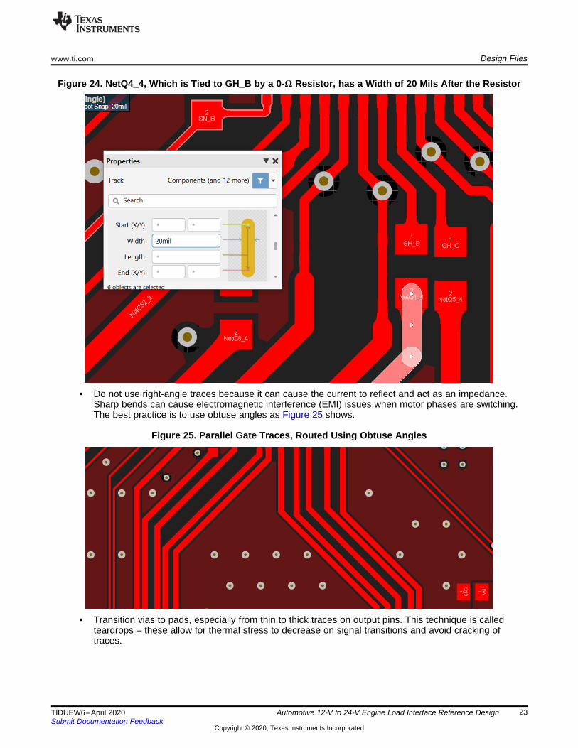
Figure 24. NetQ4_4, Which is Tied to GH_B by a 0-Ω Resistor, has a Width of 20 Mils After the Resistor
• Do not use right-angle traces because it can cause the current to reflect and act as an impedance.Sharp bends can cause electromagnetic interference (EMI) issues when motor phases are switching.The best practice is to use obtuse angles as Figure 25 shows.
Figure 25. Parallel Gate Traces, Routed Using Obtuse Angles
• Transition vias to pads, especially from thin to thick traces on output pins. This technique is calledteardrops – these allow for thermal stress to decrease on signal transitions and avoid cracking oftraces.

Design Files www.ti.com
24 TIDUEW6–April 2020Submit Documentation Feedback
Copyright © 2020, Texas Instruments Incorporated
Automotive 12-V to 24-V Engine Load Interface Reference Design
Figure 26. Teardrops Used on Transitions From Vias to Pads
For high-current nets, polygon pours are implemented to create wide current paths for phase currents,power nodes on signal layers, and power rails on the POWER layer.
In the TIDA-060030 design, polygon pours are implemented using the following system diagram by layer:• POWER
1. VBAT – battery net2. VM – large net that connects to VM of the power management circuitry, bypass caps of the
DRV8343S-Q1, and VM nodes of the power stage bulk capacitances3. 6V_BUCK – net that runs to or from the 6-V buck converter4. 3.3V_LDO – net that powers all logic-level circuitry, including C2000, LEDs, and input controls
• GND - Large GND pour over entire layer• BOTTOM
1. VM – pour that connects to the recirculation diode on the BOTTOM layer and VM on the POWERlayer
2. OUT_C1 – connects to OUT_C1 on top layer3. OUT_C2 – connects to OUT_C2 on top layer4. GND pour everywhere else
• TOP1. Similar nets (typically in power management and power stage circuitry) are connected together
where possible such as VM, 6V_BUCK, output nets, and VBAT2. GND pour everywhere else
4.1.3.6 Bulk and Bypass Capacitor Placement
4.1.3.6.1 Bulk Capacitor PlacementIn a motor drive system design, a bulk capacitor minimizes the effects of low-frequency current transientand stores charge to supply large currents required by the motor driver when it switches. When selecting abulk capacitor, consider the highest current required by the motor system, supply voltage ripple, and typeof motor.
www.ti.com Design Files
25TIDUEW6–April 2020Submit Documentation Feedback
Copyright © 2020, Texas Instruments Incorporated
Automotive 12-V to 24-V Engine Load Interface Reference Design
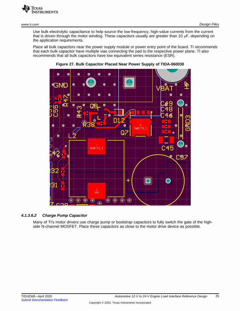
Use bulk electrolytic capacitance to help source the low-frequency, high-value currents from the currentthat is driven through the motor winding. These capacitors usually are greater than 10 μF, depending onthe application requirements.
Place all bulk capacitors near the power supply module or power entry point of the board. TI recommendsthat each bulk capacitor have multiple vias connecting the pad to the respective power plane. TI alsorecommends that all bulk capacitors have low equivalent series resistance (ESR).
Figure 27. Bulk Capacitor Placed Near Power Supply of TIDA-060030
4.1.3.6.2 Charge Pump CapacitorMany of TI's motor drivers use charge pump or bootstrap capacitors to fully switch the gate of the high-side N-channel MOSFET. Place these capacitors as close to the motor drive device as possible.

Design Files www.ti.com
26 TIDUEW6–April 2020Submit Documentation Feedback
Copyright © 2020, Texas Instruments Incorporated
Automotive 12-V to 24-V Engine Load Interface Reference Design
Figure 28. Charge Pump Capacitor Placement
4.1.3.6.3 Bypass and Decoupling Capacitors
4.1.3.6.3.1 Near Power SupplyA bypass capacitor is used to minimize high-frequency noise into the supply pin of the DRV device. TIrecommends placing capacitors as close as possible to the power input pins of the device and groundpins. If the trace lengths between the bypass capacitor and the device are not minimized, they can beinductive at the high frequencies that the bypass capacitor is meant to filter. The added impedance fromtrace inductance can cause ringing in the voltage or current at the supply pin which contributes to EMI andaffects the performance of digital or analog circuits. A best practice is to place the capacitor with the lesservalue as close as possible to the device to minimize the influence of the inductance of the trace.

www.ti.com Design Files
27TIDUEW6–April 2020Submit Documentation Feedback
Copyright © 2020, Texas Instruments Incorporated
Automotive 12-V to 24-V Engine Load Interface Reference Design
Figure 29. Decoupling Capacitors Placed Near 3.3-V LDO Power Supply
• Do not use vias between the bypass capacitors and the active device. Visualize the high-frequencycurrent flow and reduce loops of high-frequency current as much as possible.
• Make sure bypass capacitors are on the same layer as active components for best results. Do notplace a via between the bypass capacitor pin and the IC supply or ground pin.
4.1.3.6.3.2 Near Power StageFor bypass capacitance on the power stage, use small ceramic capacitors to attenuate high-frequencycurrents caused by switching from the MOSFETs and other parasitic capacitances. These capacitorstypically have values of capacitance less than 10 μF, depending on the application requirements.
4.1.3.6.3.3 Near Switch Current SourceCorrect layout and placement of these capacitors is critical to make sure they are effective. Any additionalparasitic inductance between the capacitance and the source of the switching current decreases theireffect. Ideally, place the capacitors as close as possible to the source of the switching currents, in thiscase, the motor and MOSFETs.

Design Files www.ti.com
28 TIDUEW6–April 2020Submit Documentation Feedback
Copyright © 2020, Texas Instruments Incorporated
Automotive 12-V to 24-V Engine Load Interface Reference Design
Figure 30. Bulk Capacitor Placed Near Switching Current Source in the Same VM Pour
4.1.3.6.3.4 Near Current Sense AmplifiersFor devices with integrated current sense amplifiers (CSA), TI recommends placing additional decouplingcapacitors as close to the sensing pins as possible and using values of approximately 1 nF.

www.ti.com Design Files
29TIDUEW6–April 2020Submit Documentation Feedback
Copyright © 2020, Texas Instruments Incorporated
Automotive 12-V to 24-V Engine Load Interface Reference Design
Figure 31. Decoupling Capacitors Placed Near SNx and SPx Pins
4.1.3.6.3.5 Near Voltage RegulatorsFor devices with voltage regulators, place the capacitor as close as possible to the pin. Minimize theground return loop to the ground pin.
Figure 32. Decoupling Capacitor Placed Near DVDD Pin
4.1.3.7 MOSFET Placement and Powerstage RoutingPlacement of the gate driver and power MOSFETs is critical for correct functionality and optimalperformance in pre-driver motor drive solutions. In the TIDA-060030 design, the bottom half of the board isspecifically dedicated to the power stage routing for optimal current dissipation, eliminating switch-noderinging, and efficient switching of current to the output loads.

Design Files www.ti.com
30 TIDUEW6–April 2020Submit Documentation Feedback
Copyright © 2020, Texas Instruments Incorporated
Automotive 12-V to 24-V Engine Load Interface Reference Design
Each output phase of TIDA-060030 has a unique layout optimized for its configuration. Phases have twoexternal FETs for the GHx and GLx signals, but only phases B, C high, and C low have recirculationdiodes to dissipate current and protect the load in the case both FETs are turned off independently. Eachphase also is optimized in consideration of high-current loop paths to minimize overall loop inductance,voltage ripple, noise, and the need for extra bypass capacitance.
4.1.3.7.1 Phase A: Unidirectional BDC MotorPhase A supports a unidirectional brushed-DC motor or solenoid load. One end of the load is connectedto OUT_A1, and the other end is connected to either GND or VM. If the load is a brushed-DC motor, thenthe motor will spin in only one direction depending on the motor configuration. Likewise, a solenoid loadwill push or pull depending on the load configuration.
The system is rated for up to 15 A of current, so it recommended to have traces at least 150 mil wide toefficiently sink high current. Outputs of the powerstage use polygon pours to support high current flow andprotect the board and components from any cracks in traces.
All phase A gate drive signals use 20-mil traces, and VSEN_A uses a 10-mil trace because they are low-current signals.
Figure 33. Power Stage Layout for Phase A
4.1.3.7.2 Phase B: Solenoid With Half-bridgePhase B supports a solenoid output using a half-bridge configuration that provides short-to-battery andshort-to-ground protection. The solenoid load is connected to OUT_BH and OUT_BL. A recirculation diodeis placed in parallel with the load to dissipate current in the case the drivers are switched off. Likewise withphase A, power stage signals that can detect the full solenoid load current are to be 10 mil wide for every1 A.
All phase B gate drive signals use 20-mil traces, and VSEN_B uses a 10-mil trace because they are low-current signals.

www.ti.com Design Files
31TIDUEW6–April 2020Submit Documentation Feedback
Copyright © 2020, Texas Instruments Incorporated
Automotive 12-V to 24-V Engine Load Interface Reference Design
Figure 34. Power Stage Layout for Phase B
4.1.3.7.3 Phase C: Independent Loads Using Split Half-BridgePhase C supports two solenoid outputs using a split half-bridge configuration, a capability provided by theDRV8343S-Q1 device using independent FET mode. In this mode, the high-side and low-side drivers canindependently drive two separate loads such as solenoids and unidirectional brushed-DC motors. In thelayout, there exists two separate current paths to drive the output loads independently. Each topologyrequires a recirculation diode in parallel with the output load to dissipate current when the driver is off.
The solenoid load for the high side of phase C (CH) is connected to OUT_CH, and the low side isconnected to GND. Likewise, the solenoid load for the low side of phase C (CL) is connected to OUT_CL,and the high side is connected to VM.
All phase C gate drive signals use 20-mil traces, and VSEN_CH and VSEN_CL use a 10-mil tracebecause they are low-current signals.

Design Files www.ti.com
32 TIDUEW6–April 2020Submit Documentation Feedback
Copyright © 2020, Texas Instruments Incorporated
Automotive 12-V to 24-V Engine Load Interface Reference Design
Figure 35. Power Stage Layout for Phase C High-Side and C Low-Side
4.1.3.8 Current Sense Amplifier RoutingMany of TI’s motor drivers include built-in current sensing, most of which use an external shunt resistor asthe measurement source. Including the current sense amplifier with the driver provides an all-in-onesolution for the motor interface and allows higher-quality current sensing at a lower cost.
Two-phase and three-phase CSAs are a benefit to board layout because they have low common-modevoltage requirements. They also let each channel be measured individually, and therefore can be used inmore complex control schemes such as field-oriented control (FOC).
The tradeoffs of using two-phase and three-phase CSAs in board layout include:• Higher susceptibility to ground noise• Cannot detect ground shorts• Could require more software to realize the total system current
For placement, the shunt resistor should be in line with the components of the power stage to minimizetrace impedance. The shunt resistor should also be placed close to the connection to the CSA to decreasethe possibility of coupling on other traces on the board. The shunt resistor should be placed between thesource of the respective low-side MOSFET and the ground connection.
Use the copper pours from the source of the low side to tie to the high side of the CSA. The sense signalsof the shunt resistors should be a differential pair and traces must run in parallel to the input of the IC.

www.ti.com Design Files
33TIDUEW6–April 2020Submit Documentation Feedback
Copyright © 2020, Texas Instruments Incorporated
Automotive 12-V to 24-V Engine Load Interface Reference Design
Figure 36. Shunt Resistor Placement Between Low-Side MOSFET and Ground
4.1.3.9 Net TiesWhen routing a PCB during the initial stages, the guides that help show which component routes can bedeceptive in the case of the sense resistor routing. In the case of the low-side shunt resistor, the negativeinput could direct straight to ground, and the positive input could direct to the low-side source pin. Toavoid these situations, place a Net Tie between the device and the shunt resistor so that the designer canplace the route restriction during placement instead of during routing.

Design Files www.ti.com
34 TIDUEW6–April 2020Submit Documentation Feedback
Copyright © 2020, Texas Instruments Incorporated
Automotive 12-V to 24-V Engine Load Interface Reference Design
Figure 37. Net Ties in Layout Figure 38. Net Ties in Layout, Zoomed in
4.2 Gerber FilesTo download the Gerber files, see the design files at TIDA-060030.
4.3 Assembly DrawingsTo download the assembly drawings, see the design files at TIDA-060030.
5 Related Documentation1. Texas Instruments, DRV8343-Q1 12-V / 24-V Automotive Gate Driver Unit (GDU) with Independent
Half Bridge Control and Three Integrated Current Sense Amplifiers Data Sheet2. Texas Instruments, LMR36006-Q1 4.2-V to 60-V, 0.6-A Ultra-Small Synchronous Step-Down
Converter Data Sheet3. Texas Instruments, TPS7B81-Q1 150-mA, Off-Battery, Ultra-low-IQ (3-μA), Low-Dropout Regulator
Data Sheet4. SQJ850EP Automotive N-Channel 60 V (D-S) 175 °C MOSFET Vishay Siliconix www.vishay.com5. FSV20100V Ultra-Low VF Schottky Rectifier, 20 A, 100 V Data Sheet ON Semiconductor
www.onsemi.com6. Texas Instruments, TMS320F2803x Piccolo™ Microcontrollers Data Sheet7. Texas Instruments, TMS320F2803x Piccolo™ Technical Reference Manual8. Texas Instruments, Best Practices for Board Layout of Motor Drivers Application Report9. Texas Instruments, Using DRV to Drive Solenoids - DRV8876/DRV8702-Q1/DRV8343-Q1 Application
Report

www.ti.com Related Documentation
35TIDUEW6–April 2020Submit Documentation Feedback
Copyright © 2020, Texas Instruments Incorporated
Automotive 12-V to 24-V Engine Load Interface Reference Design
5.1 TrademarksE2E, LaunchPad, Code Composer Studio, Piccolo are trademarks of Texas Instruments.WEBENCH is a registered trademark of Texas Instruments.Altium Designer is a registered trademark of Altium LLC or its affiliated companies.All other trademarks are the property of their respective owners.
5.2 Third-Party Products DisclaimerTI'S PUBLICATION OF INFORMATION REGARDING THIRD-PARTY PRODUCTS OR SERVICES DOESNOT CONSTITUTE AN ENDORSEMENT REGARDING THE SUITABILITY OF SUCH PRODUCTS ORSERVICES OR A WARRANTY, REPRESENTATION OR ENDORSEMENT OF SUCH PRODUCTS ORSERVICES, EITHER ALONE OR IN COMBINATION WITH ANY TI PRODUCT OR SERVICE.
6 TerminologyADC - analog-to-digital converterBOM - bill of materialsBuck - step-down switching-mode voltage converterC2000 - real-time control microcontroller unit, 16-, 32-bitCCS - Code Composer StudioCSA - current shunt amplifierDL - drain lowFET - field effect transistorGND - groundGH - gate highICE - internal combustion engineLDO - linear dropout voltage regulatorMCU - microcontroller unitMOSFET - metal oxide semiconductor field effect transistorOEM - original equipment manufacturerPB - push buttonPCB - printed circuit boardTIRD - TI Reference DesignVBAT - battery voltageVM - motor driver voltage, same as VBAT after filter
7 About the AuthorAARON BARRERA is an Applications Engineer at Texas Instruments. He graduated from the Universityof Florida in December 2019 with a Bachelor of Science in Electrical Engineering. Aaron works with theBLDC Motor Driver team, and previously was a Product Marketing Intern for BLDC Motor Drivers. In hisfree time, he enjoys arranging and producing music, playing basketball, and watching sports.

IMPORTANT NOTICE AND DISCLAIMER
TI PROVIDES TECHNICAL AND RELIABILITY DATA (INCLUDING DATASHEETS), DESIGN RESOURCES (INCLUDING REFERENCE DESIGNS), APPLICATION OR OTHER DESIGN ADVICE, WEB TOOLS, SAFETY INFORMATION, AND OTHER RESOURCES “AS IS” AND WITH ALL FAULTS, AND DISCLAIMS ALL WARRANTIES, EXPRESS AND IMPLIED, INCLUDING WITHOUT LIMITATION ANY IMPLIED WARRANTIES OF MERCHANTABILITY, FITNESS FOR A PARTICULAR PURPOSE OR NON-INFRINGEMENT OF THIRD PARTY INTELLECTUAL PROPERTY RIGHTS.These resources are intended for skilled developers designing with TI products. You are solely responsible for (1) selecting the appropriate TI products for your application, (2) designing, validating and testing your application, and (3) ensuring your application meets applicable standards, and any other safety, security, or other requirements. These resources are subject to change without notice. TI grants you permission to use these resources only for development of an application that uses the TI products described in the resource. Other reproduction and display of these resources is prohibited. No license is granted to any other TI intellectual property right or to any third party intellectual property right. TI disclaims responsibility for, and you will fully indemnify TI and its representatives against, any claims, damages, costs, losses, and liabilities arising out of your use of these resources.TI’s products are provided subject to TI’s Terms of Sale (www.ti.com/legal/termsofsale.html) or other applicable terms available either on ti.com or provided in conjunction with such TI products. TI’s provision of these resources does not expand or otherwise alter TI’s applicable warranties or warranty disclaimers for TI products.
Mailing Address: Texas Instruments, Post Office Box 655303, Dallas, Texas 75265Copyright © 2020, Texas Instruments Incorporated