Automatic Flow for Library Cell Optimization with Synopsys ...
17
© Copyright by Synopsys Inc. / MunEDA GmbH & Inc., all rights reserved Improve Design Performance and Yield Automatic Flow for Library Cell Optimization with Synopsys HSpice ® & MunEDA WiCkeD TM © Copyright by Synopsys Inc. / MunEDA GmbH & Inc., all rights reserved Improve Design Performance and Yield 2 LEGAL NOTICE Information contained in this presentation reflects Synopsys’ and MunEDA‘s plans as of the date of this presentation. Such plans are subject to completion and subject to change. Products may be offered and purchased only pursuant to an authorized quote and purchase order.
Transcript of Automatic Flow for Library Cell Optimization with Synopsys ...

© Copyright by Synopsys Inc. / MunEDA GmbH & Inc., all rights reserved
Improve DesignPerformance and Yield
Automatic Flow for Library Cell Optimization with Synopsys HSpice® & MunEDA WiCkeDTM
© Copyright by Synopsys Inc. / MunEDA GmbH & Inc., all rights reserved
Improve DesignPerformance and Yield
2
LEGAL NOTICEInformation contained in this presentation reflects Synopsys’ and MunEDA‘s plans as of the date of this presentation. Such plans are subject to completion and subject to change. Products may beoffered and purchased only pursuant to an authorized quote and purchase order.

© Copyright by Synopsys Inc. / MunEDA GmbH & Inc., all rights reserved
Improve DesignPerformance and Yield
3
Nanometer Yield Limiters
• Functional Yield (DfM)– Geometry distortion due to optical aberration– Opens and shorts due to defects (catastrophic faults)
• Crosstalk failures (Signal integrity)– Coupling of adjacent signals– Coupling through power grid and substrate
• Static and dynamic IR drop• Thermal variation• Parametric Yield (DfY)
– Performance degradation due to variability during manufacturing– Chip functions but does not meet specifications
• Jitter and phase noise• Age dependent degradation (Reliability)
– Electromigration– NBTI, HCI, and gate oxide reliability
© Copyright by Synopsys Inc. / MunEDA GmbH & Inc., all rights reserved
Improve DesignPerformance and Yield
4
Parametric Variability will Dominate Yield Loss
20
30
40
50
60
70
80
90
100
350 250 180 130 90Technology nodes (nm)
Prod
uct y
ield
(%)
Lithography & new material-based yield
Design-based yield
Defect densityyield
65, 45
Source: IBS Report

© Copyright by Synopsys Inc. / MunEDA GmbH & Inc., all rights reserved
Improve DesignPerformance and Yield
5
Examples of Variations
Litho Variation Gate Oxide Variation
Source: IBM
© Copyright by Synopsys Inc. / MunEDA GmbH & Inc., all rights reserved
Improve DesignPerformance and Yield
6
Paradox of Increasing Variation
180nm 130nm 90nm 65nmManufacturing Process Node
45nm
Variations Increase For Each Process Node
Source: Synopsys
TargetPerformance

© Copyright by Synopsys Inc. / MunEDA GmbH & Inc., all rights reserved
Improve DesignPerformance and Yield
7
Variability in Nanometer Technologies
• Higher fractional (%) variability with finer design rules & larger wafers (Table source ITRS)
• Lower voltages – less head room• High speed & RF functions in CMOS• Pressure to ramp products to volume & early profitability• Mask costs $1M at 90nm, $2M at 65nm
L 250 nm 180 nm 130 nm 90 nm 65 nm 45 nmVt (mV) 450 400 330 300 280 200�Vt (mV) 21 23 27 28 30 32
�Vt/Vt 4.7% 5.8% 8.2% 9.3% 10.7% 16%
© Copyright by Synopsys Inc. / MunEDA GmbH & Inc., all rights reserved
Improve DesignPerformance and Yield
8
Parametric Variation Components
• Global (inter-die-variations)– From chip to chip, across wafer, across lots– Influence all devices of a circuit the same way– Constant variance– For example: tox
• Local (intra-die-variations)– Influence all devices of a circuit differently– Variance depends on device area:– Increasingly important for digital– For example: �L, vfb
• Spatial– Due to process and thermal gradients– Not important for small blocks
• Proximity dependent– Mostly systematic
LW �� 12local�

© Copyright by Synopsys Inc. / MunEDA GmbH & Inc., all rights reserved
Improve DesignPerformance and Yield
9
Variation Components (Fab)
• Fabs differ in equipment, geographic location, and process control policies
• Equipment capability is better in fabs that are constructed later and they have tighter distributions
• Even if the nominal or fast case are aligned between fabs, the spread is different
• Either use larger spreads or change pricing policy and charge a premium for the better fabs
Fab 1 Fab 2
Critical Parameter
Non-critical Parameter
Upper Limit
Upper Limit
Lower Limit
Lower Limit
Source: Synopsys
© Copyright by Synopsys Inc. / MunEDA GmbH & Inc., all rights reserved
Improve DesignPerformance and Yield
10
Variation Components (Lot, Wafer)
• Processes drift over time till– Parameter reaches SPC limit
– Equipment is cleaned
– There is a yield bust
• Latest fabs cost $2B and have much better monitoring and feedback-feedforward control
• Wafers in a lot tend to have a linear and/or quadratic gradient depending on their position
Time
Wafer#
+Par
amet
er
Source: Synopsys

© Copyright by Synopsys Inc. / MunEDA GmbH & Inc., all rights reserved
Improve DesignPerformance and Yield
11
• Wafer variation comes from fab, lot, wafer processes
• Linear variation is due to materials and gas flow
• Radial variation is due to thermal and spin processes
• Wafer level variation is the sum of wafer, linear, and radial variation
• Affects mainly single-ended circuit performance measures like switching speed, gain, dynamic power etc.
Wafer Variation Linear Variation
Radial Variation Wafer Level Variation
Variation Components (Wafer)
Source: Synopsys
© Copyright by Synopsys Inc. / MunEDA GmbH & Inc., all rights reserved
Improve DesignPerformance and Yield
12
• Reticle variation is due to photo processes
• Local variation comes from totally random microscopic processes. It affects mainly differential circuit performance measures like differential amplifier offset voltage, current mirrors, DACs, etc. Becoming important for digital design (30% of global variation at 130nm).
• Total parametric variation combines wafer, reticle, and local variations
Across Reticle Variation Across Wafer Variation
Non-local Variation Local Variation
Variation Components (Reticle, Local)
Source: Synopsys

© Copyright by Synopsys Inc. / MunEDA GmbH & Inc., all rights reserved
Improve DesignPerformance and Yield
13
Influence of Process Variations on Digital Cells
Leak
age
DelaySource: Intel
© Copyright by Synopsys Inc. / MunEDA GmbH & Inc., all rights reserved
Improve DesignPerformance and Yield
14
Why Optimize Cell Libraries?
• Cells in the library are the basic building blocks of all ASICS
• Nanometer libraries have from 500 to 5,000 cells
• Library generation and creation is highly automated process
• Any improvement in performance and yield of the library cells has extremely high payoff as it is reflected in all future products that use the library
• Associated costs are amortized across the large numbers of instances of a cell on a given design and across multiple designs

© Copyright by Synopsys Inc. / MunEDA GmbH & Inc., all rights reserved
Improve DesignPerformance and Yield
15
Optimization—An Example Setup
Optimization target• Power—reduce leakage and dynamic power
– Given: Process variations, operating conditions
Optimization constraints• Minimal worsening of slew rate and delay• Minimal increase in active area
Optimization variables• Length and width of NMOS and PMOS transistors
© Copyright by Synopsys Inc. / MunEDA GmbH & Inc., all rights reserved
Improve DesignPerformance and Yield
16
Synopsys/MunEDA — Automatic ASIC Library Optimization
� Automated optimization for performance and yield of digital and analog cell libraries
� Minimal and easy user interaction
� GUI to set technology/library specific geometric constraints and objectives
� Cell optimization controlled by automatically generated customizable Tcl-scripts
� Folds seamlessly into current digital cell layout and characterization flows and uses the same infrastructure/hardware
© Copyright by Synopsys Inc. / MunEDA GmbH & Inc., all rights reserved
Improve DesignPerformance and Yield
17
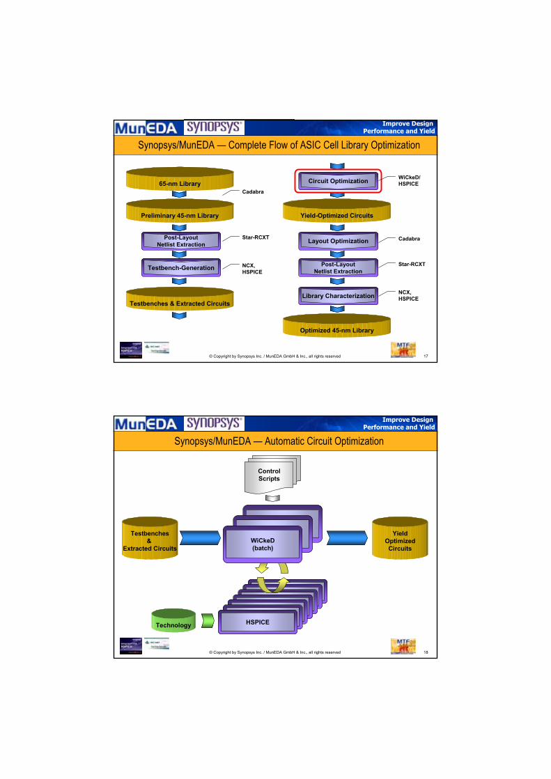
Synopsys/MunEDA — Complete Flow of ASIC Cell Library Optimization
65-nm Library
Preliminary 45-nm Library
Testbenches & Extracted Circuits
Yield-Optimized Circuits
Optimized 45-nm Library
Post-LayoutNetlist Extraction
Testbench-Generation
Circuit Optimization
Layout Optimization
Post-LayoutNetlist Extraction
Library Characterization
Cadabra
Star-RCXT
NCX,HSPICE
WiCkeD/HSPICE
Cadabra
Star-RCXT
NCX,HSPICE
© Copyright by Synopsys Inc. / MunEDA GmbH & Inc., all rights reserved
Improve DesignPerformance and Yield
18
HSPICE
Synopsys/MunEDA — Automatic Circuit Optimization
Testbenches&
Extracted Circuits
YieldOptimizedCircuits
WiCkeD(batch)
Technology
ControlScripts

© Copyright by Synopsys Inc. / MunEDA GmbH & Inc., all rights reserved
Improve DesignPerformance and Yield
19
GUI-Concept of Setup Tool
© Copyright by Synopsys Inc. / MunEDA GmbH & Inc., all rights reserved
Improve DesignPerformance and Yield
20
GUI-Concept of Setup Tool

© Copyright by Synopsys Inc. / MunEDA GmbH & Inc., all rights reserved
Improve DesignPerformance and Yield
21
Results—Histogram & Density Estimate
Leakage
Den
sity
Density EstimatePopulation (i.e. infinite samples)
Histogram:Limited samples (e.g. 1000)
Example results for 65nm library
© Copyright by Synopsys Inc. / MunEDA GmbH & Inc., all rights reserved
Improve DesignPerformance and Yield
22
Results—NAND-Gate
Leakage
Den
sity
Delay (Rise)
Den
sity
Leakage• Median leakage reduced by 37%• Standard deviation reduced by 35%
Delay• Median delay increased by 5%• Small increase in active area
Example results for 65nm library

© Copyright by Synopsys Inc. / MunEDA GmbH & Inc., all rights reserved
Improve DesignPerformance and Yield
23
Results—Summary
Example results for 65nm library
• Average yield improvement of 11%– Yield: Percentage of circuits meeting given specification
• Variability reduction of 25%-35%• Tradeoff
– Area increase 10%– Delay increase max. 5% (constraint for optimization)
Cell Transistors Design Parameters
YieldImprovement
invd2 4 6 + 9%
buffd4 12 10 + 10%
nd2d2 8 11 + 13%
mux2d2 14 26 + 11%
© Copyright by Synopsys Inc. / MunEDA GmbH & Inc., all rights reserved
Improve DesignPerformance and Yield
24
Conclusion
• Considering process variations becomes increasingly important for digital cells
• Time pressure for library qualification requires automated optimization
• Optimization tool a must for tradeoff analysis
• Synopsys/MunEDA library migration flow successfully addressesprocess variations
• Promising results from first library migration (65 nm)
© Copyright by Synopsys Inc. / MunEDA GmbH & Inc., all rights reserved
Improve DesignPerformance and Yield
25
Contact
Synopsys
Chris Labrecquev) +1 650.584.5553c) +1 650.380.6939e) [email protected]
MunEDA
Andreas Rippv) +49 89 / 9 30 86-3 35c) +49 1 72 / 8 64 35 19e) [email protected]
Frank Schenkelv) +49 89 / 9 30 86-3 36e) [email protected]
© Copyright by Synopsys Inc. / MunEDA GmbH & Inc., all rights reserved
Improve DesignPerformance and Yield
Backup Slides

© Copyright by Synopsys Inc. / MunEDA GmbH & Inc., all rights reserved
Improve DesignPerformance and Yield
27
Local Process Variations
• Source:– Line edge roughness
– finite number of dopant atoms
– gate oxide variation
• Local variations cause a production-induced asymmetry of symmetrically designed devices � Mismatch
Lgate Vth tox
Figures from IBM
© Copyright by Synopsys Inc. / MunEDA GmbH & Inc., all rights reserved
Improve DesignPerformance and Yield
28
Trend of Local Variations on Digital Cells
10 50 90 130
Leff (nm)
0%
20%
40%
60%
�I o
n/I o
n
32nm
45nm
65nm
90nm180nm 250nm
20% Leff variation
12% Nch variation
Source: IBM
© Copyright by Synopsys Inc. / MunEDA GmbH & Inc., all rights reserved
Improve DesignPerformance and Yield
29
Trend of Local Variations on Analog Cells
0.111 %
10 %
100 %
1000 %
I rel
Leff (μm)
Data: K. Bult (ESSCIRC 2000)
© Copyright by Synopsys Inc. / MunEDA GmbH & Inc., all rights reserved
Improve DesignPerformance and Yield
30
Variation Components (Proximity)
• Properties depend on orientation, proximity to other features, and presence of covering metal or fill pattern
• Important for analog and high performance digital including cell based designs
• Deterministic systematic variation that can be modeled and/or mask compensated
Device
Metal or Fill
Source: Synopsys

© Copyright by Synopsys Inc. / MunEDA GmbH & Inc., all rights reserved
Improve DesignPerformance and Yield
31
With OPCNo OPC
Original Layout
OPC Corrections
Source: Synopsys
Optical Proximity Correction (OPC)
• Corrective modifications to improve process control– improve yield (process window)– improve device performance
© Copyright by Synopsys Inc. / MunEDA GmbH & Inc., all rights reserved
Improve DesignPerformance and Yield
32
Variation Components (Spatial)
• Process, thermal, and stress gradients lead to position dependent variation
• Important for analog (DAC, ADC, PLL, CDR) and clock skew on large digital chips
• Typical value in literature is 1%/mm
x
7.5% within chip variation
Zuchowski et al (IBM) ICCAD 2004
Device
yGradient
Device
© Copyright by Synopsys Inc. / MunEDA GmbH & Inc., all rights reserved
Improve DesignPerformance and Yield
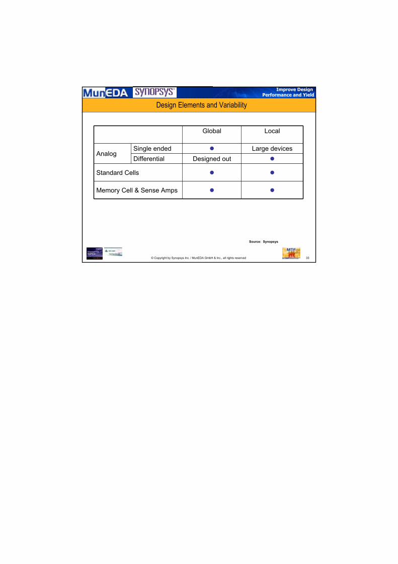
33
Design Elements and Variability
Global Local
AnalogSingle ended � Large devicesDifferential Designed out �
Standard Cells � �
Memory Cell & Sense Amps � �
Source: Synopsys