Author: Egon Pavlica Nova Gorica Polytechic Comparision of Metal-Organic Semiconductor interfaces to...
22
Author: Egon Pavlica Nova Gorica Polytechic Comparision of Metal- Organic Semiconductor interfaces to Metal- Semiconductor interfaces May 2003
-
Upload
lucy-farmer -
Category
Documents
-
view
219 -
download
0
Transcript of Author: Egon Pavlica Nova Gorica Polytechic Comparision of Metal-Organic Semiconductor interfaces to...

Author: Egon Pavlica
Nova Gorica Polytechic
Comparision of Metal-Organic Semiconductor interfaces to Metal-
Semiconductor interfaces
May 2003
● Introduction to Organic Semiconductors
● Inorganic Semiconductor surfaces
● Metal-Inorganic Semiconductor interfaces
● Metal-Organic Semiconductor interfaces
● Conclusion
Contents:
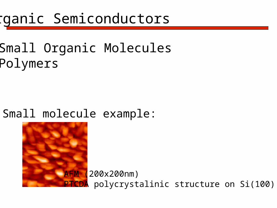
Organic Semiconductors
● Small Organic Molecules● Polymers
AFM (200x200nm)PTCDA polycrystalinic structure on Si(100)
Small molecule example:

Organic SemiconductorsOrganic SemiconductorsOrganic Semiconductors
Polymer example:
SEM of Polyaniline thin film deposited in vacuum on mica, silicon and mcroporous silicon

Organic Semiconductors
Electronic Polarization cloud - Electronic polaron

Organic Semiconductors
Molecular polaron Lattice polaron

Energy diagram of dinamic polaron statesin anthracene type crystals
Organic Semiconductors

Space-Charge Layers
Tight-binding model:- smaller overlap integral- surface state levels- donor states: empty positive- acceptor states: full negative- generally states are mixed

Space-Charge Layers
Charge neutrality
Depletion layer
Acceptor states

Space-Charge Layers
Depletion:- low major carr.conc.Inversion:- high minor carr.conc.Accumulation:- high Ds states- free charge
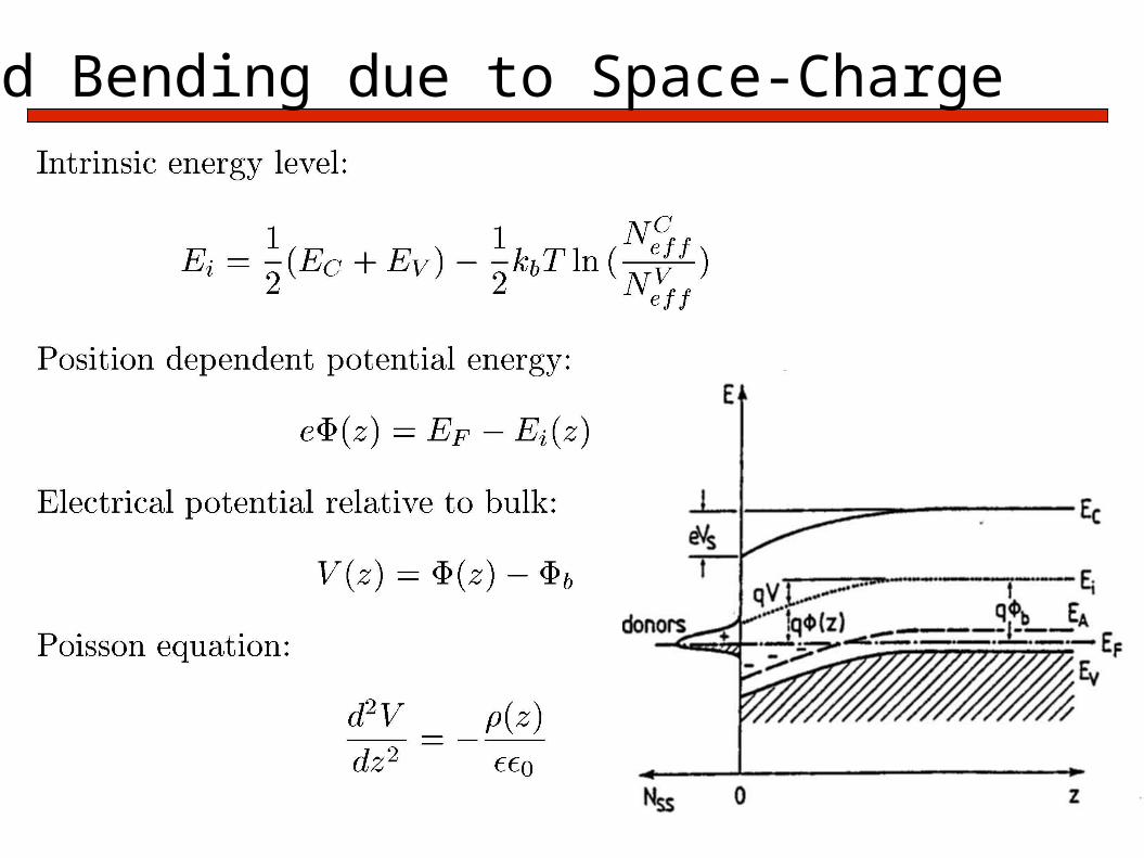
Band Bending due to Space-Charge

Schottky Depletion Space-Charge Layer
Band bending V(surface)>>kT
Approximation of space charge density
Electric field
Electric potential energy
Band bending:

Band bending - Inorganic semiconductors
Weak space-charge layer
Strong space-chare layer
Schottky layer
Calculated band bending due to acceptor/donor surface state levelfor GaAs
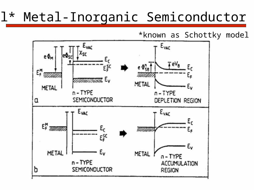
Ideal* Metal-Inorganic Semiconductor*known as Schottky model
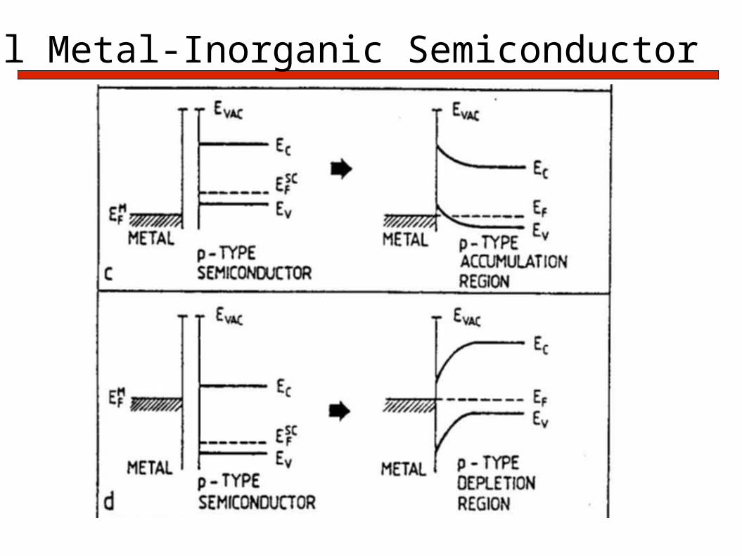
Ideal Metal-Inorganic Semiconductor

Bardeen model
Facts:●Metal atoms in close contact with semiconductor form chemical bonds●Charge flow in bonds....formation of dipole layer●Interdiffusion●Formation of new electronic interface states●Both model fails to explain the barrier height dependence on metal work function
Model approximations:●Interface region●Surface states of clean semiconductor persist and pin Fermi level

VIGS and MIGS
Deposited metals produce interface states
Virtualy Induced Gap States in semiconductor are matched to Conduction band of metal
Induced surface states are of mixed acceptor/donor character
Fermi level near cross-over energy EB

Metal-Organic semiconductors
Band model of semiconductor:●Neglible doping●No intrinsic carriers●Wide band gap ~ 2 eV●No band bending●Low mobility < 0.1cm2/Vs●Dielectric constat low ~ 3

Metal-Organic semiconductors
Band model of semiconductor:●No depletion layers●Space Charge Limited Currents●Image potential is important

Metal-Organic semiconductors
Hopping model●Interfaces currently relevant only to charge transport simulations ●Monte Carlo simulations●Gaussian Distribution of state energies
An succesful attempt to understand current-voltage characteristics includedinteface dipoles, image charge effects and phonons in bulk

Conclusions
● No theory of metal-organic semiconductor interfaces, since too specific.
● Band models are based on different structure, so are fundamentally incorrect.
● The hopping models and localized states are promising theory for metal-organic semiconductor interfaces.