AT-1 - Atlantic Technology THX HT Speaker Solutions
12
Flexible Auto-Refresh: Enabling Scalable and Energy-Efficient DRAM Refresh Reductions Ishwar Bhati * , Zeshan Chishti § , Shih-Lien Lu § , and Bruce Jacob ¶ * Oracle Corporation § Intel Corporation ¶ University of Maryland * [email protected], § {zeshan.a.chishti, shih-lien.l.lu}@intel.com, ¶ [email protected] Abstract Capacitive DRAM cells require periodic refreshing to preserve data integrity. In JEDEC DDRx devices, a refresh operation is carried out via an auto-refresh command, which refreshes multiple rows from multiple banks simultaneously. The internal implementation of auto-refresh is completely opaque outside the DRAM—all the memory controller can do is to instruct the DRAM to refresh itself— the DRAM handles all else, in particular determining which rows in which banks are to be refreshed. This is in conflict with a large body of research on reducing the refresh overhead, in which the memory controller needs fine-grained control over which regions of the memory are refreshed. For example, prior works exploit the fact that a subset of DRAM rows can be refreshed at a slower rate than other rows due to access rate or retention period variations. However, such row-granularity approaches cannot use the standard auto-refresh command, which refreshes an entire batch of rows at once and does not permit skipping of rows. Consequently, prior schemes are forced to use explicit sequences of activate (ACT) and precharge (PRE) operations to mimic row-level refreshing. The drawback is that, compared to using JEDEC’s auto- refresh mechanism, using explicit ACT and PRE commands is inefficient, both in terms of performance and power. In this paper, we show that even when skipping a high percentage of refresh operations, existing row-granurality refresh techniques are mostly ineffective due to the inherent efficiency disparity between ACT/PRE and the JEDEC auto- refresh mechanism. We propose a modification to the DRAM that extends its existing control-register access protocol to include the DRAM’s internal refresh counter. We also introduce a new “dummy refresh” command that skips refresh operations and simply increments the internal counter. We show that these modifications allow a memory controller to reduce as many refreshes as in prior work, while achieving significant energy and performance advantages by using auto-refresh most of the time. *This work was done while Ishwar Bhati was a graduate student at University of Maryland. Permission to make digital or hard copies of all or part of this work for personal or classroom use is granted without fee provided that copies are not made or distributed for profit or commercial advantage, and that copies bear this notice and the full citation on the first page. To copy otherwise, to republish, to post on servers or to redistribute to lists, requires prior specific permission and/or a fee. ISCA’15, June 13-17, 2015, Portland, OR USA 1. Introduction To retain the data stored in their leaky capacitive cells, DRAMs require periodic refresh operations, which incur both performance and energy overheads. As DRAM devices get denser, three primary refresh penalties increase significantly: The time spent occupying the command bus with refresh commands increases with the number of rows to be refreshed; the time during which rows are unavailable because their storage capacitors are being recharged increases with the number of simultaneous rows being refreshed (among many other factors); and the power needed to keep the DRAM system refreshed scales with the number of capacitors in the system. These overheads are already significant and are on the rise. Refresh is projected to account for up to 50% of the DRAM power while simultaneously degrading memory throughput by 50% in future 64Gb devices [1]. Therefore, practical and scalable mechanisms to mitigate refresh penalties will be crucial in future systems with large main memories. As is well known, a large number of refreshes are unnecessary and therefore can be skipped by utilizing either access or retention period awareness. Access awareness exploits knowledge of recent read/write activity, as refresh operations to a row can be skipped if the row has been accessed recently, or if the data stored in it are no longer required [2], [3]. Retention awareness exploits knowledge of the characteristics of individual cells. The retention period of a DRAM cell indicates how frequently it should be refreshed to preserve its stored charge. Importantly, among all cells, most have high retention (on the order of few seconds), while a very few “weak” cells have low retention that requires frequent refreshes [4], [5]. For simplicity, in commodity DRAM, the refresh rate for the entire device is specified by a single retention period (tRET), representing the worst-case time of the weakest cells. Consequently, prior retention-aware schemes characterize and store retention period per-row and then selectively schedule frequent refreshes to only the rows with weak cells, thereby reducing as many as 75% of the refreshes [1], [6]. The problem facing these prior schemes is that JEDEC’s refresh mechanism in DDRx DRAMs takes away fine- grained control of refresh operations, thereby rendering row- level refresh-reduction techniques relatively inefficient, or worse, unusable. Prior refresh reduction schemes, both retention and access aware, rely on a fine-granularity row-level refresh option to selectively refresh only the required rows. However, such a row-level refresh command is no longer supported in
Transcript of AT-1 - Atlantic Technology THX HT Speaker Solutions

Flexible Auto-Refresh: Enabling Scalable and Energy-Efficient DRAM Refresh Reductions
Ishwar Bhati*, Zeshan Chishti
§, Shih-Lien Lu§, and Bruce Jacob
¶
*Oracle Corporation
§Intel Corporation
¶University of Maryland
§{zeshan.a.chishti, shih-lien.l.lu}@intel.com,
Abstract Capacitive DRAM cells require periodic refreshing to
preserve data integrity. In JEDEC DDRx devices, a refresh
operation is carried out via an auto-refresh command,
which refreshes multiple rows from multiple banks
simultaneously. The internal implementation of auto-refresh
is completely opaque outside the DRAM—all the memory
controller can do is to instruct the DRAM to refresh itself—
the DRAM handles all else, in particular determining which
rows in which banks are to be refreshed.
This is in conflict with a large body of research on
reducing the refresh overhead, in which the memory
controller needs fine-grained control over which regions of
the memory are refreshed. For example, prior works exploit
the fact that a subset of DRAM rows can be refreshed at a
slower rate than other rows due to access rate or retention
period variations. However, such row-granularity
approaches cannot use the standard auto-refresh command,
which refreshes an entire batch of rows at once and does
not permit skipping of rows. Consequently, prior schemes
are forced to use explicit sequences of activate (ACT) and
precharge (PRE) operations to mimic row-level refreshing.
The drawback is that, compared to using JEDEC’s auto-
refresh mechanism, using explicit ACT and PRE commands
is inefficient, both in terms of performance and power.
In this paper, we show that even when skipping a high
percentage of refresh operations, existing row-granurality
refresh techniques are mostly ineffective due to the inherent
efficiency disparity between ACT/PRE and the JEDEC auto-
refresh mechanism. We propose a modification to the
DRAM that extends its existing control-register access
protocol to include the DRAM’s internal refresh counter.
We also introduce a new “dummy refresh” command that
skips refresh operations and simply increments the internal
counter. We show that these modifications allow a memory
controller to reduce as many refreshes as in prior work,
while achieving significant energy and performance
advantages by using auto-refresh most of the time.
*This work was done while Ishwar Bhati was a graduate student at
University of Maryland.
Permission to make digital or hard copies of all or part of this work
for personal or classroom use is granted without fee provided that
copies are not made or distributed for profit or commercial
advantage, and that copies bear this notice and the full citation on
the first page. To copy otherwise, to republish, to post on servers or
to redistribute to lists, requires prior specific permission and/or a
fee.
ISCA’15, June 13-17, 2015, Portland, OR USA
1. Introduction To retain the data stored in their leaky capacitive cells,
DRAMs require periodic refresh operations, which incur
both performance and energy overheads. As DRAM devices
get denser, three primary refresh penalties increase
significantly: The time spent occupying the command bus
with refresh commands increases with the number of rows
to be refreshed; the time during which rows are unavailable
because their storage capacitors are being recharged
increases with the number of simultaneous rows being
refreshed (among many other factors); and the power
needed to keep the DRAM system refreshed scales with the
number of capacitors in the system.
These overheads are already significant and are on the
rise. Refresh is projected to account for up to 50% of the
DRAM power while simultaneously degrading memory
throughput by 50% in future 64Gb devices [1]. Therefore,
practical and scalable mechanisms to mitigate refresh
penalties will be crucial in future systems with large main
memories.
As is well known, a large number of refreshes are
unnecessary and therefore can be skipped by utilizing either
access or retention period awareness. Access awareness
exploits knowledge of recent read/write activity, as refresh
operations to a row can be skipped if the row has been
accessed recently, or if the data stored in it are no longer
required [2], [3]. Retention awareness exploits knowledge of
the characteristics of individual cells. The retention period
of a DRAM cell indicates how frequently it should be
refreshed to preserve its stored charge. Importantly, among
all cells, most have high retention (on the order of few
seconds), while a very few “weak” cells have low retention
that requires frequent refreshes [4], [5]. For simplicity, in
commodity DRAM, the refresh rate for the entire device is
specified by a single retention period (tRET), representing
the worst-case time of the weakest cells. Consequently, prior
retention-aware schemes characterize and store retention
period per-row and then selectively schedule frequent
refreshes to only the rows with weak cells, thereby reducing
as many as 75% of the refreshes [1], [6].
The problem facing these prior schemes is that JEDEC’s
refresh mechanism in DDRx DRAMs takes away fine-
grained control of refresh operations, thereby rendering row-
level refresh-reduction techniques relatively inefficient, or
worse, unusable.
Prior refresh reduction schemes, both retention and access
aware, rely on a fine-granularity row-level refresh option to
selectively refresh only the required rows. However, such a
row-level refresh command is no longer supported in
JEDEC DDRs. To get around this limitation, prior
implementations explicitly send an activate (ACT)
command followed by a precharge (PRE) command to the
desired DRAM row [7, 8].
In comparison, JEDEC’s Auto-Refresh (AR) command,
which refreshes several rows simultaneously, is typically
used for refresh operations in DDRx devices. To simplify
refresh management, the memory controller is given limited
responsibility in the refresh process: it only decides when an
AR should be scheduled based on a pre-specified refresh
interval (tREFI). The DRAM device controls what rows to
be refreshed in an AR operation and how refresh is
implemented internally. A refresh counter is maintained by
the device itself to track the rows to be refreshed in next
AR. More importantly, device designers have optimized AR
by exploiting knowledge of how the DRAM bank is
internally organized in multiple sub-arrays. Each sub-array
carries out refresh operations independently; therefore the
DRAM can schedule several refreshes in parallel to multiple
rows of a single bank, thereby reducing both the
performance and energy penalties of refresh.
Our key observation is that neither mechanism — neither
AR by itself nor prior schemes that are forced to use ACT
and PRE to realize row-level refresh — are optimal in
minimizing the performance and power impact of refresh.
Since the memory controller does not have enough control
over refresh with AR, it cannot skip unnecessary refreshes at
all, and using ACT/PRE to refresh individual rows is simply
not scalable to future DRAM devices.
For perspective: to accomplish row-level refresh, a 16Gb
DDR4 x4 device [7], will require four million ACT and
PRE commands (8M total commands)1 in each tRET
(64ms). If directed to an individual bank, this would require
13ms to complete; if directed to all banks at once, this would
require 25ms to complete2. In contrast, in each tRET (64ms)
period, auto-refresh requires only 8K AR commands, three
orders of magnitude fewer commands on the command bus
compared to the per-row scheme, with each operation
completing in tRFC (480ɳs) time [9]. Hence, AR satisfies
all bank refresh in 3.93ms (8K*480ɳs), which is 3.3X and
6.4X less than the time required by the row-level option for
single and all banks, respectively. Furthermore, the energy
consumption of row-level refresh (details in Section 2.5) is
also substantially higher than the optimized AR option.
Thus, even if most of the refreshes are skipped, the inherent
inefficiencies of row-level ACT/PRE refresh prevent one
from obtaining the desired refresh reduction benefits.
The purpose of this work, therefore, is to make the
already optimized AR mechanism flexible enough so that a
memory controller can skip unwanted refreshes while
serving the rest of refreshes efficiently. We therefore
1 Each bank of 16Gb device (4 bit wide) has 256K rows, and a total of
4M rows in all of its 16 banks. 2 ACT on same and different banks must wait for tRC (50ɳs) and tRRD
(6ɳs) respectively. Thus, row-level refresh consumes 13.1ms (256K*50ns) to refresh a single bank, and 25.1ms (4M*6ɳs) to refresh all banks.
propose a simple DRAM modification to provide external
access to the refresh counter register, by extending the
register-access interface already available in the latest
commodity DDR4 and LPDDR3 devices. This interface
allows the memory controller to write or read pre-defined
mode registers through Mode Register Set (MRS) or Mode
register Read (MRR or MPR) commands [7], [10]. For
instance, in DDR4, the on-die temperature sensor value can
be read by accessing a specific register with an MPR
command. We propose that the refresh counter value be
accessed using the same MRS/MPR mechanism.
In addition, we introduce a “dummy-refresh” command,
which increments the internal refresh counter but does not
schedule any refreshes — hence it consumes one command
bus cycle without interrupting any memory requests on any
of the internal banks.
The main contributions of this paper are as follows:
We quantify and analyze the inefficiencies caused by
JEDEC’s Auto-refresh scheme when row-granularity
refresh techniques are used, and further show that the
prior refresh reduction techniques do not scale in high
density DDRs.
We propose simple changes in DRAM to access the
refresh counter, which enable the JEDEC AR mechanism
to be utilized in refresh reduction techniques.
We quantify the effects of our proposal, Flexible Auto-
Refresh (REFLEX), serving most of the required refresh
operations through AR, while skipping refreshes through
dummy-refresh.
We show that, in 32Gb devices, REFLEX techniques save
an average of 25% more memory energy than row-level
refresh when 75% of the refreshes are skipped.
2. Background and Motivation DRAM devices require periodic refresh operations to
preserve data integrity. The frequency of refresh operations
is decided by the DRAM retention time characteristics. Prior
work has shown that retention time is not evenly distributed
among DRAM cells; most of the cells have high retention
period while very few cells (referred to as weak cells) have
low retention period. Because the number of weak cells can
be significant (e.g., tens of thousands per DRAM device
[11]), the device manufacturers specify a single retention
time (tRET) that corresponds to the weakest cells. Typically,
tRET is 64ms at normal temperature and 32ms at high
temperature [7].
Earlier “asynchronous” DRAM devices supported two
refresh commands: CAS-before-RAS (CBR) and RAS-Only
[12]. Under CBR operation, the DRAM device itself
controls the refreshing row number using an internal refresh
counter. Under RAS-Only, the memory controller manages
refresh operations for each row. Today, however, modern
synchronous DDR DRAMs, which have completely
replaced asynchronous devices, support only one refresh
mechanism: Auto-Refresh (AR).

2.1. Refresh in Commodity DRAMs
The DRAM refresh process can be logically broken up into
three distinct decisions: (i) Scheduling: when (and how
often) are refresh operations carried out, (ii) Granularity:
what portion (rows) of memory is refreshed in each refresh
operation, and (iii) Implementation: how is a refresh
operation implemented inside the DRAM.
In commodity DRAMs, the AR command is designed to
provide greater control of the refresh process to the DRAM
device itself. The memory controller is only in charge of
scheduling the refresh commands; for instance, issuing an
AR command once every refresh interval (tREFI). The
DRAM device is free to decide what rows are to be
refreshed and how the refresh operations are accomplished
internally, during the refresh completion interval (tRFC). A
refresh counter, internal to the device, tracks the set of rows
to be refreshed in the next command.
Table 1 shows a trend; as device density increases, the
number of rows grows at the same pace, and all rows must
be refreshed in a tRET (64ms) period. If refreshing a single
row at a time, 16Gb and 32Gb devices would require 4M
and 8M refresh commands per tRET, respectively; which
means a refresh command should be issued every few
nanoseconds (15.2ɳs in 16Gb and 7.6ɳs in 32Gb device).
Fortunately, JEDEC realized this scalability problem early
on and kept the tREFI period long (7.8µs for DDR3), by
allowing a single AR to refresh several rows at once. But, as
shown in Table 1, the tRFC period increases as more rows
are refreshed in an AR (512 rows in 16Gb, and 1024 in
32Gb). To address increasing tRFC values, DDR4 devices
have three refresh rate options. The default refresh rate is to
issue 8K AR commands in tRET, as in DDR3. The other
two options increase refresh rate by 2x or 4x by refreshing
half or one-fourth rows respectively, to reduce tRFC.
Lastly, an AR command can be issued at a per-bank or an
all-bank level. In commodity DDR devices, only all-bank
AR is supported, while LPDDR devices have a per-bank AR
option in addition. In the all-bank AR operation, all the
banks are simultaneously refreshed and are unavailable for
the tRFC period. In contrast, LPDDR’s per-bank AR
refreshes rows only in the addressed bank. While this
requires many more refresh commands to be issued during
the tRET period (the number increases by a factor equal to
the degree of banking), a refreshing bank is idle for a shorter
tRFCpb period (approximately half of an all-bank’s tRFC
period), and other banks can service memory requests
during the refresh operation. The advantage of all-bank AR
is that, with single command, several rows of all the banks
are refreshed, consuming less time overall than equivalent
per-bank ARs. However, since the per-bank AR option
allows non-refreshing banks to service memory requests, the
programs with high memory bank parallelism may perform
better with per-bank AR than with all-bank AR.
2.2. Self-Refresh (SR) Mode
To save background energy, DRAM devices employ low
power modes during idle periods. The lowest power mode,
known as Self-refresh (SR), turns off the entire DRAM
clocked circuitry and the DLL and triggers refresh
operations internally by a built-in analog timer without
requiring any command from the memory controller.
When in self-refresh mode, the scheduling of refresh
commands is exclusively under the control of the DRAM
device. The device automatically increments the internal
refresh counter after each refresh operation. The number of
refresh operations serviced during the SR mode would vary
depending on the time the DRAM spends in the SR mode
and how refresh operations are scheduled by the DRAM
device during that time. Consequently, when the memory
controller switches the DRAM back from the SR mode to
the active mode, the exact value of the refresh counter
cannot be correctly predicted.
2.3. Row-granularity Refreshing
Multiple prior works have attempted to exploit the fact that
a large subset of DRAM rows need to be refreshed at a
Table 1: Number of rows and refresh completion time in DDR4 devices (x4) [7], [9]. Both increase with device density. Note: K = 1024, M= 1024*1024 Device density
Num. Banks
Per-bank Rows
Total Rows
Rows in AR
tRFC (ɳs)
8Gb 16 128K 2M 256 350
16Gb 16 256K 4M 512 480
32Gb 16 512K 8M 1024 640
tRRD
tFAW(30ɳs) tRC(50ɳs)tRRD
(6ɳs)
tRRD
tFAW(30ɳs)
tRRD
tFAW(30ɳs)
tRFC(110ɳs)
tRRD
(6ɳs)tRRD
(6ɳs)
For DDR3 1Gb x8 device, timing comparison of explicit row-level refreshes (top) equivalent to an Auto-Refresh (AR)
command (bottom). Single AR refreshes 2 rows in each of the eight banks.
Figure 1: An illustration (in 1Gb DDR3 devices) of Row-level refresh timing constraints compared with an auto-refresh (AR)
command. An AR, in this case, refreshes two rows in each of the 8 banks.
slower than nominal rate. Since most DRAM cells have high
retention periods, prior retention aware techniques exploit
row-granularity refreshing to reduce a large number of
unnecessary refreshes [1], [6]. For instance, the previously
proposed RAIDR scheme skips 75% of refresh operations
by storing the measured retention time profile at a row
granularity and issuing or skipping refresh to a row based on
its retention period. A second set of refresh reduction
techniques, such as Smart refresh [2] and ESKIMO [3], skip
refresh to a row if the row has been recently accessed or
data stored in it are no longer needed for future accesses.
Both these sets of techniques rely on row-level refresh
granularity to reduce the required number of refreshes.
Current DDR devices do not support row-level refresh
commands like RAS-Only in the earlier asynchronous
devices. As described in Section 2.1, managing refresh at
the row granularity is problematic, especially with millions
of rows in DDR devices. Therefore JEDEC has deprecated
row-granularity refresh command. The only way row-
granularity refresh can be implemented in current devices is
by explicitly issuing a sequence of ACTIVATE followed by
a PECHARGE command for each row. In the next two
subsections, we present performance and energy overheads
of Auto-Refresh and explicit row-level refresh.
An alternative to the explicit ACTIVATE-PRECHARGE
sequence is for the DRAM device to internally keep track of
rows which require less frequent refreshing and to skip
refreshes to such rows in response to AR commands from
the memory controller. However, such an implementation
has two important drawbacks: First, it would require
additional storage and logic inside the DRAM to maintain a
record (such as a bit vector or a table) of the weak vs. strong
rows. For commodity devices, such logic and storage may
be prohibitive in terms of cost. Second, for techniques
which rely on access awareness, such as Smart refresh [2]
and ESKIMO [3], the DRAM device will need to keep track
of when a row was last accessed. These limitations constrain
DRAM-exclusive solutions for row-granularity refreshing
without any involvement from the memory controller.
2.4. Performance Overheads of Refresh
The time required for refresh is growing exponentially with
each generation, as the time required scales with the number
of bits to refresh. The advantage of JEDEC’s optimized
auto-refresh mechanism is that, as rows are added to each
generation, the device is also banked to a finer degree, and
the internal refresh mechanism refreshes more rows in
parallel. Explicit row-level refresh cannot exploit this
parallelism, because the sub-array organization is not visible
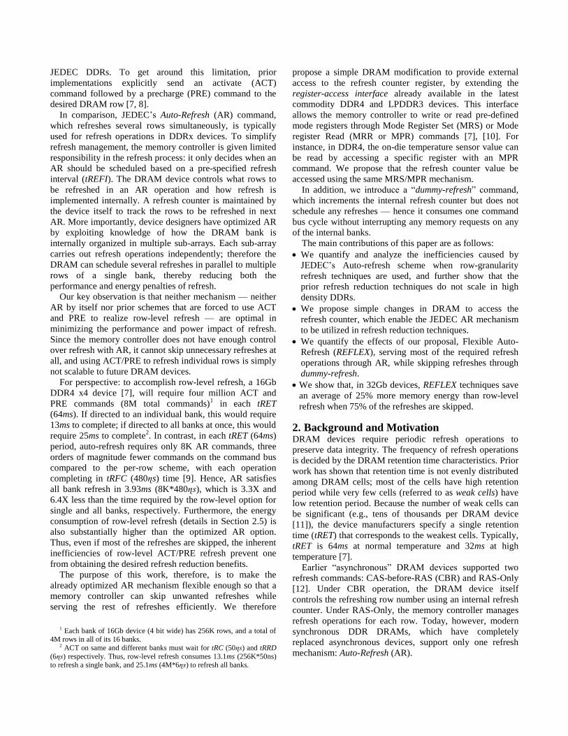
outside the DRAM [13]. Figure 2 quantifies the difference;
the figure shows refresh time in milliseconds as DRAM
density increases for all-bank AR; this is compared to the
individual row-level option, given different degrees of
refresh reductions (labeled % skip). The skip percentage
represents a refresh reduction scheme’s ability to eliminate
that percentage of refresh operations. Note that, for the row-
level results, refresh time is shown per-bank, assuming an
ideal case for row-level refresh in which all banks can
schedule refreshes in parallel. Specifically, the graph shows
that, for a 16Gb device, even if 70% of the refreshes are
eliminated, the time to complete the remaining 30% is equal
to using AR on all the rows.
Another timing detail to note is that the DRAM device in
all-bank AR is permitted to activate rows faster than the
tRRD and the tFAW constraints, as the power dissipation of
an AR is known and optimized. By contrast, when using
ACT to perform row-level refresh, one must observe both
tRRD and tFAW to meet the DRAM power constraints, as
illustrated in Figure 1. Lastly, since row-level refresh blocks
Figure 2: Time required in explicit row-level vs auto-refresh as DRAM density increases. The % skip correspond to unnecessary
refreshes. In16Gb devices, row-level refresh with 70% rows skipped only evens out with auto-refresh.
auto-refresh (AR)
0% skip
30% skip
50% skip
70% skip
90% skip 0
10
20
30
512Mb 1Gb 2Gb 4Gb 8Gb 16Gb 32Gb
Tim
e (m
illis
eco
nd
s)
Minimum time refresh operations occupy (in milliseconds) in a refresh window (tREFW),
with increasing device density
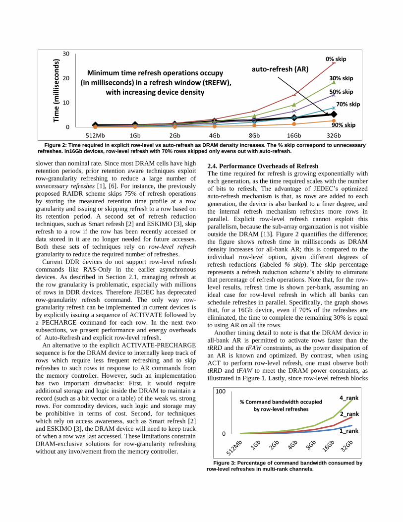
Figure 3: Percentage of command bandwidth consumed by
row-level refreshes in multi-rank channels.
1_rank
2_rank
4_rank
0
100
% Command bandwidth occupied by row-level refreshes

only the refreshing bank, while allowing other banks to
service memory requests concurrently, workloads with high
bank-level parallelism can get better performance compared
with all-bank AR. However, we observe that a more
efficient way of utilizing this bank-level parallelism is to
implement per-bank AR instead of relying on row-level
refreshes. For example in 16Gb DDR4 x4 devices, if per-
bank AR is used, then refreshing a single bank requires only
1.97ms (assuming LPDDR3 trends of tRFCpb half of tRFC),
which is 15% of the row-level option.
Finally, issuing ACT/PRE commands can consume
substantial command bandwidth, and the situation worsens
as the number of ranks sharing the command bus increases.
For instance, a rank using 32Gb devices requires 16M (8M
ACT and 8M PRE) commands to satisfy row-level refresh,
and in a four-ranked channel all 64M commands for refresh
are scheduled on a common bus. As shown in Figure 3, the
required bandwidth for row-level refreshes approaches
100% of the total available command bandwidth (assuming
64ms refresh window and 1600Mbps devices). Thus, row-
level refresh commands leave little command bandwidth for
normal memory requests (reads and writes).
2.5. Energy Overheads of Refresh
To compare the energy consumed by an AR command
and one ACT/PRE sequence for row-level refresh, we use
the equations below [14].
Ear = (IDD5-IDD3N)*tRFC*Vdd
Eact/pre = (IDD0*tRC – IDD3N*tRAS – IDD2N (tRC-tRAS))*Vdd
We use timing and IDD current values based on the 16Gb
JEDEC DDR4 datasheet and Table 4 in [9] respectively.
The values are as follows: IDD0=20mA, IDD3N=15.5mA,
IDD2N=10.1mA, and IDD5=102mA; tRC=50ns,
tRAS=35ns, and tRFC=480ns. IDD0 and IDD3N values for
x8 devices are scaled down to the smaller row size in x4
devices. Using these parameters, the energy consumed by
one AR command is as follows: Ear = (102–15.5)*480 =
41.5nJ.3 The energy consumed by one set of ACT/PRE
commands is Eact/pre = 20*50 – 15.5*35 – 10.1*15 = .306nJ.
Since an AR schedules 32 row-refreshes in each of the 16
banks, we have Erow-level = Eact/pre*32*16 = 157nJ. Hence, the
energy consumed by row-level refreshes (Erow-level) is almost
four times Ear, the energy consumed by an AR command.
Furthermore, on average in the 16Gb device, an ACT
should be scheduled in each 15.2ns (64ms/4M) interval for
row-level refresh. This means that the DRAM device does
not have the opportunity to switch to low power modes and
needs to stay in the “active” mode most of the time, where it
consumes high background power. Lastly, as described in
Section 2.2, when a DRAM device is in the self-refresh (SR)
mode, the scheduling of refreshes has to be carried out by
the device itself. This implies that upon switching back to
3 In calculations, Vdd of 1V is assumed. For energy unit conversion
from ɳs*mA*V to ɳJ, former value is divided by 1000 to get ɳJ.
active mode, the row-level refresh scheme needs to know
which rows were refreshed during the SR mode, so that the
refresh operations can be resumed from the correct point.
However, lack of access to the internal device refresh
counter makes it difficult for a row-level refresh scheme to
resume refresh correctly. This difficulty makes row-level
refreshes incompatible with the SR mode, further worsening
the energy consumption, when the device is idle.
3. Flexible Auto-Refresh As we have shown, the JEDEC auto-refresh mechanism is
incompatible with the refresh reduction techniques that
exploit row-level awareness. We propose a modification of
the DRAM access protocol that would return control to the
memory controller’s heuristics without sacrificing the
optimizations in JEDEC auto-refresh. We note that the
DRAM refresh counter value is not accessible externally,
yet control-register-access mechanisms exist in the JEDEC
DDR specs. If, somehow, the memory controller could
access and change the refresh counter, then as we will show,
our proposed techniques could reduce as many refreshes as
the individual row-level heuristics, while issuing most of the
remaining refreshes through the optimized AR mechanism.
3.1. Refresh Counter Access Architecture
We observe that current DRAM devices already have an
interface available to read and write internal DRAM
registers [7], [10]. We propose to extend the existing
interface to include the refresh counter, thereby making the
refresh counter both readable and writeable by the memory
controller.
Figure 4 shows the details of our proposed DRAM
architecture. Reading the refresh counter register (REFC-
READ) can be implemented similar to MPR (multi-purpose
register) reads in DDR4 or MRR (mode register read) in
LPDDR3 devices [7], [10]. In response to a “REFC-READ”
command (Figure 4(c)), the DRAM returns the refresh
counter value on its data bus like a normal control register
read. Since the refresh counter is accessed infrequently, only
at initialization and on exit from self-refresh (SR) mode,
timing overheads are not critical. Using the refresh counter
access feature, the memory controller knows the rows to be
refreshed in the next AR command and can also find exactly
how many refreshes happened during the previous self-
refresh (SR) mode.
To skip refresh operations, the memory controller should
be able to increment the refresh counter without actually
performing refresh operations. We propose to add such a
command, referred to as “dummy-refresh”. As shown in
Figure 4(b), “dummy-refresh” can be implemented to share
the command-code (RAS and CAS asserted) with normal
auto-refresh (AR), with one address bit used as a flag to
differentiate it from AR. Since “dummy-refresh” causes no
real refresh activity and merely increments the internal
refresh counter, it does not have the performance or energy
overheads of regular refresh operations. For instance, the
memory controller can issue normal memory requests while

a “dummy-refresh” operation is being serviced.
Furthermore, “dummy-refresh” is easily extendible to have
all the existing AR variations, like per-bank (LPDDR3) and
DDR4 fine-grained (x2, x4) options by incrementing the
appropriate number of rows in the refresh counter.
Finally, a “REFC-WRITE” command, as shown in Figure
4(d), can overwrite the value of the refresh counter register,
implemented as another Mode Register Set (MRS)
command [7]. The REFC-WRITE command can be used to
synchronize all the devices in a rank after exiting from SR
mode. In SR mode, the DRAMs issue refreshes based on
timing events generated from their local ring oscillators. The
timings of oscillators in each device are not synchronized,
and therefore some devices in a rank may issue more
refreshes than others while in SR mode. In this scenario, the
refresh counter values read from devices at SR exit may not
match exactly. Subsequently, a REFC-WRITE can be used
to synchronize the rank by explicitly writing a common
minimum value to the refresh counters of all devices.
3.2. Flexible Auto-Refresh (REFLEX) Techniques
Through the proposed architecture, the memory controller
can access and synchronize the refresh counter values of all
devices in a rank or system. The memory controller can use
“dummy-refresh” commands to skip refreshes when needed.
We propose a set of three refresh reduction mechanisms,
collectively referred to as Flexible Auto-Refresh (REFLEX).
In DDR devices, the default refresh option is to issue 8K
all-bank AR (1x granularity mode) commands in a tRET
period. Two other options added in DDR4 are to increase
the refresh issue rate to 16K and 32K AR in the retention
period (2x and 4x granularity modes respectively). These
finer granularity options decrease the number of rows
refreshed in a single AR command. Our first proposed
technique called REFLEX-1x, issues auto-refresh (AR) and
“dummy-refresh” using only the default 1x refresh
granularity option. When using REFLEX-1x, the memory
controller tracks refresh requirements at the granularity of
all rows refreshed in a single AR command (we refer to
them as AR bins).
Figure 5 illustrates the workings of REFLEX techniques.
For simplicity, only 32 rows of a device are shown and two
of them (row 7 and row 20) have weak cells. Rows with
weak cells need to be refreshed in each tRET round whereas
other rows need to be refreshed infrequently (for example,
once in every 4 tRET rounds). In the example, each 1x AR
command refreshes 8 rows in all banks. Therefore the
baseline scheme needs to send four AR commands so that
all 32 rows are refreshed (Figure 5(a)). In the REFLEX-1x
scheme, the memory controller schedules refresh commands
only if there are weak rows among the rows refreshed in an
AR, otherwise a “dummy-refresh” is issued to increment the
refresh counter. Therefore, as shown in Figure 5(b),
REFLEX-1x issues only two AR commands corresponding
to the AR bins including the two weak rows, whereas two
“dummy-refresh” commands are issued, reducing the overall
refresh activity by a factor of two.
The previously proposed RAIDR work [1] characterized
the DRAM retention time behavior and showed that only up
to 1K rows in a 32GB DRAM system require refresh times
of less than 256ms. RAIDR refreshes these 1K weak rows
once every 64ms, while refreshing the remaining strong
rows once every 256ms (or one-fourth of the worst-case
rate). Therefore, by employing row-granularity refreshes
and skipping unnecessary refreshes to strong rows, RAIDR
is able to achieve a 74.6% reduction in refresh activity. In
comparison, REFLEX-1x employs the standard AR
command, which, when directed to a weak row, also
unnecessarily refreshes the strong rows in the AR bin.
However, even in the worst case, when all the 1K rows are
in separate AR bins, REFLEX-1x can reduce 65% of refresh
operations, because in a 256ms period, the baseline AR
scheme issues 32K (8K per 64ms) AR commands, while
REFLEX-1x would issue only 11K (1K + 1K + 1K + 8K)
AR commands.
REFC-READ
CLK
CMD
ADDR
DATA
tCL
REFCReg. Addr
Refresh Counter value
REFC-WRITE
CLK
CMD
ADDR
DATA
tMRD/tMOD
REFCReg. Addr
REFC Value
VALID**
DUMMY-REF
CLK
CMD
ADDR
DATA
REFC-FLAG
VALID**
Command/AddressDecode
Refresh Counter Reg.
BANKS
Command Bus
Data Bus
REFC
-REA
D
REFC
-WRI
TE
DU
MM
Y/A
R
REFRESH TIMINGS & MANAGEMENT
Update/read
MU
X
.
.
.REFC-READ command
puts ref. counter value on Data Bus
REFC-WRITE, DUMMY and Auto Refresh update ref. counter
Refresh Commands1) AUTO-REFRESH (AR)2) DUMMY REFRESH3) REFC-READ4) REFC-WRITE
Address Bus
(a) Proposed Refresh Architecture (b) DUMMY-REFRESH command
(c) REFC-READ command (d) REFC-WRITE command Figure 4: Our proposed changes in DRAM for flexible auto-refresh. Three new commands are added to access, write and increment
the refresh counter register. **VALID in (b) and (d) refers to any allowed command.

Our second technique, referred to as REFLEX-4x, utilizes
the finer granularity 4x AR option introduced in DDR4. In
REFLEX-4x, retention or access awareness is stored at the
granularity of rows refreshed in one 4x AR command. In
16Gb devices, 1x and 4x AR options refresh 512 and 128
rows respectively. Therefore, the amount of storage required
in the controller increases for REFLEX-4x compared with
REFLEX-1x. However, REFLEX-4x has the ability to issue
finer-grained refreshes to reduce more unnecessary refresh
operations. For further optimization, the memory controller
may intermingle REFLEX-1x and REFLEX-4x operations as
needed. As shown in Figure 5(c), REFLEX-4x refreshes only
4 rows, reducing 75% of refresh operations compared with
the baseline. Furthermore, REFLEX-4x when used in the
RAIDR characterization settings reduces 72.5% of refresh
operations, almost equal to what row-level refreshes in
RAIDR could achieve (74.6%).
The tradeoff by using 1x AR and finer-granularity AR is
between refresh bin storage and the number of eliminated
refresh operations. In REFLEX-1x, since 8K AR are
scheduled in a tRET, only 8K bins are required in a rank.
Assuming 2 bit storage for each bin (for example, indicating
retention time of 64, 128, 192 or 256 ms), REFLEX-1x
requires 2KB of storage per rank. However, because of the
larger refresh granularity in the REFLEX-1x technique, the
potential of refresh reduction is less compared with the
finer-grained REFLEX-4x scheme.
Finally, in our third technique referred to as REFLEX-
Row, the memory controller manages the DRAM on a per
row basis, as done in RAIDR. In the REFLEX-Row scheme,
the memory controller issues ACT-PRE (same as row-level
refresh) commands to only weak rows in the next AR bin.
After that, a “dummy-refresh” operation is issued to
increment the refresh counter. An example of REFLEX-Row
is shown in Figure 5(d). To reduce the amount of storage
required in the controller, an intelligent scheme using bloom
filters as proposed in RAIDR can be employed [1].
REFLEX-Row achieves as much refresh reduction as
previous row-level based retention aware techniques, while
satisfying most refresh requirements through the standard
AR mechanism and issuing row-level refreshes only for the
handful of weak rows.
3.3. REFLEX using per-bank AR
The auto-refresh command has two types, as described in
Section 2.1: all-bank and per-bank AR. The advantage of
per-bank AR is that, when one bank is refreshing, other
banks can service memory requests concurrently, whereas
all-bank AR makes all banks unavailable during refresh. As
suggested in a recent study[15], adding a support similar to
LPDDR type per-bank AR in general purpose DDR devices
should not be difficult, requiring only simple changes: an
extra flag on the DDR interface to differentiate per-bank
from all-bank AR, a corresponding change in the command
decoder to identify this flag, a new counter storing the bank
number, and a logic component that increments the refresh
counter when the bank counter rolls over to 0. Per-bank AR
(tRFCpb) requires around 40% to 50% of the time required
by all-bank AR (tRFC). For instance, in an 8Gb LPDDR3
device, tRFC is 210ɳs while tRFCpb is 90ɳs [10].
REFLEX-1x techniques can work in per-bank AR in a
similar manner as in all-bank AR. Since per-bank AR is
issued at a finer granularity, the REFLEX-1x technique with
per-bank AR can eliminate more refreshes. For example,
REFLEX-1x with per-bank AR will reduce 74.2% of refresh
001230456
7 (WEAK)089
1011012
131415016
171819020 (WEAK)
212223024
252627028
293031
BANKSRefresh Counter: 0
Refresh Counter: 8
Refresh Counter:8
Refresh Counter: 16
Refresh Counter: 16
Refresh Counter: 24
Refresh Counter:24
Refresh Counter: 32
Auto-Refresh #1
Auto-Refresh #2
Auto-Refresh #3
Auto-Refresh #4
Refresh Counter: 0
Refresh Counter: 8
Refresh Counter:8
Refresh Counter: 16
Refresh Counter: 16
Refresh Counter: 24
Refresh Counter:24
Refresh Counter: 32
Auto-Refresh #1
Dummy-Refresh #1
Auto-Refresh #2
Dummy-Refresh #2
001230456
7 (WEAK)89
101112131415016
171819020 (WEAK)
212223024
252627028
293031
Refresh Counter: 0
Refresh Counter: 8
Refresh Counter:8
Refresh Counter: 16
Refresh Counter:24
Refresh Counter: 32
Dummy-refresh(4x) #1
Dummy-Refresh (1x) #1
Dummy-Refresh (1x) #2
001230456
7 (WEAK)89
101112131415016
171819020 (WEAK)
212223024
252627028
293031
Refresh Counter: 2
Refresh Counter: 4
Refresh Counter: 6
Dummy-refresh(4x) #2
Dummy-refresh(4x) #3
Auto-refresh(4x) #1
Refresh Counter: 16
Refresh Counter: 24
Dummy-refresh(4x) #4Refresh Counter: 18
Refresh Counter: 20
Refresh Counter: 22
Dummy-refresh(4x) #5
Auto-refresh(4x) #2
Dummy-refresh(4x) #6
Refresh Counter: 0
Refresh Counter: 8
Refresh Counter:8
Refresh Counter: 16
Refresh Counter: 16
Refresh Counter: 24
Refresh Counter:24
Refresh Counter: 32
Dummy-Refresh #1
Dummy-Refresh #2
Dummy-Refresh #3
Dummy-Refresh #4
001230456
7 (WEAK)89
101112131415016
171819020 (WEAK)
212223024
252627028
293031
Row- Level Refresh #1 ( row 7, bank 0)
Row- Level Refresh #2 ( row 20, bank 0)
(a) AUTO-REFRESH (b) REFLEX-1x (Using 1x auto-refresh mode)
(d) REFLEX-Row (Mixing row-level and AR) (c) REFLEX-4x (Mixing 4x and 1x AR)
Figure 5: An illustration of how REFLEX techniques reduce refresh operations. This example shows a device with 32 rows containing two weak rows (row #7 and #20). (a) A baseline scheme with AR requires to refresh all rows (b) Dummy-Refresh only at 1x granularity (c) Dummy-Refresh at 4x granularity. (d) Mixing row-level refresh and AR options.

operations in a device with 16 banks. We propose that given
the small changes required to implement per-bank AR,
DDRs should also adopt a per-bank AR feature similar to
LPDDRs.
3.4. REFLEX with Non-Sequential Row Mappings
So far, workings of REFLEX techniques assume that the
mapping of refresh counter to row addresses is sequential
and can be easily inferred by the memory controller. But
there could be exceptions, as JEDEC gives full flexibility of
refresh implementation to the DRAM vendors. One solution
to this problem is that JEDEC can specify allowed mapping
configurations and the vendor can include the chosen
configuration into a configuration register. The memory
controller will read this register and reconstruct mappings
accordingly. Given the mapping, REFLEX techniques can
appropriately decide between AR and “dummy-refresh”.
Another scenario in which row addresses are not directly
mapped is in the presence of repair rows. To increase yield,
typically defective rows are mapped to spare regions called
repair rows. Subsequently, accesses to repair rows happen
only via indirection through a mapping table, which keeps
track of the mapping between defective rows and their
replacements from the spare region. All DRAM accesses
(including activates and refreshes) consult this table before
accessing the DRAM array. Since the characterization of
rows into strong/weak categories is carried out via standard
DRAM write/read operations, any attempt to characterize a
defective row will actually result in the repair row being
classified instead. After the characterization, any subsequent
AR operations, which map to the defective row, will also be
internally routed to the repair row. Therefore, our techniques
should work naturally with repair rows.
Finally, in our characterization we assume that the weak
rows are randomly distributed. This assumption is based on
prior work [27] showing that retention failures do not
exhibit significant spatial correlation. Our assumption is
conservative: if the weak rows are more clustered, REFLEX
techniques will be even more effective since more low cost
“dummy-refresh” operations can be scheduled.
3.5. Variable Retention Time (VRT) and Temperature
Profiling and characterizing row retention is a relevant but
not-fully-settled problem. One complication is that the
retention period of a row can change with time and
temperature. A number of studies focus on this problem
[27], [29]. For example, a recent study [29] shows that
augmenting the profiling mechanisms with SECDEC-ECC
and some guardbanding can mitigate almost all VRT-related
failures.
In contrast to the prior work on profiling, our paper deals
with a related but different problem: given that one could
characterize strong vs. weak rows, how would one design a
practical and energy-efficient mechanism that enables fine-
grained refresh control without intrusive device changes.
Proposed REFLEX mechanisms are general enough to work
in conjunction with any profiling mechanisms.
At higher temperatures, the retention period shortens, and
therefore the distribution of rows in strong and weak bins
also changes. A separate profile at higher temperature is
used to decide refresh rate for rows [1]. Once the correct
profile is enabled, our techniques would work as-is.
3.6. Refresh Reduction in SR Mode
With the proposed refresh architecture, a memory controller
can synchronize the refresh counter on an as-needed basis.
Therefore, REFLEX techniques are capable of switching the
DRAM to the lowest power self-refresh (SR) mode when
the DRAM is idle for sufficiently long periods. To further
save energy in SR mode, the refresh rate can be reduced
when switching to SR mode based on, for example, the
retention period of the upcoming rows to be refreshed. Even
if some rows have weak cells, those rows can be refreshed
through explicit row-level refresh commands before
switching to SR mode. This scheme is similar to the partial
array self-refresh (PASR) option in LPDDR devices where
unused memory locations are programmed to skip refreshes
in SR mode [10].
4. Evaluation Methodology We use a full-system x86 simulator called MARSSx86 [17]
to evaluate our proposed work. MARSSx86 is configured,
as shown in Table 2, to model four out-of-order superscalar
cores. For main memory, we integrate the cycle-accurate
DRAMSim2 simulator [18] with MARSSx86. We modify
DRAMSim2 to incorporate DDR4 bank-group constraints,
various refresh options and low power modes. The memory
Table 3: DRAM timing (in 1.25ɳs clock cycles) and current (in mA) parameters used in the simulations
Parameter DDR4 16Gb (x4) DDR4 32Gb (x4)
tRRD 4 4
tRRD_L 5 5
tRAS 28 28
tRC 40 40
tFAW 16 16
tRFC 384 512
tRFCpb 200 260
tRFC_4x 208 280
IDD0 20 23
IDD1 25 30
IDD2P 6.4 7
IDD2N 10.1 12.1
IDD3P 7.2 8
IDD3N 15.5 17
IDD4R 57 60
IDD4W 55 58
IDD5 102 120
IDD6 6.7 8
IDD7 95 105
Table 2: CPU and memory configurations used in the simulations
Processor 4 cores, 2GHz, out-of-order, 4-issue per core
L1 Cache Private, 128KB, 8-way associativity, 64B Block Size, 2 cycle latency
L2 Cache Shared, 8MB, 8-way associativity, 64B Block Size, 8 cycle latency
Memory 1 Channel, 2 Ranks per channel, 64bit wide
Memory controller
Open page, FR-FCFS [28], 64-entry queues (per-rank), address mapping: page interleaving
DRAM DDR4, x4, 1600Mbps, 16 banks, 4 bank groups
controller and DRAM configurations are shown in Table 2.
Table 3 lists the relevant DRAM timing and current (IDD)
values used in our simulations. The IDD values are used to
calculate the DRAM energy following the methodology
described in [14].
To evaluate and compare our proposed flexible auto-
refresh techniques, we implement the following refresh
options: (i) all-bank AR, (ii) per-bank AR, and (iii) explicit
row-level refresh through ACT and PRE commands. Strong
and weak rows are assigned randomly for a range of
possible “skip” percentages. Our baseline refresh scheme
employs an all-bank AR option with 0% skipping. In
simulating the row-level refresh mechanism, to evenly
distribute refresh amongst banks, a given row is refreshed in
all banks before the next row gets refreshed, a policy similar
to the one employed in RAIDR [1]. Finally, in per-bank AR,
refresh commands are sequentially issued to each bank.
When a per-bank or row-level refresh is happening on a
particular bank, other banks are allowed to operate on
memory requests with appropriate timing constraints.
We conduct our evaluations by using multi-programmed
and multi-threaded workloads from the SPEC CPU2006
suite [19] and the NAS parallel benchmark suite [20]. All
the multi-programmed workloads, except mix, consist of
four copies of the same program. The mix workload uses
four different programs (milc, gromacs, wrf, sjeng). We use
input sets ref in SPEC and CLASS C in NPB benchmarks.
Programs are executed for 4 billion instructions, starting
from the program’s region of interest (RoI) determined by
SimPoint 3.0 [21]. The workloads have a good mix of low
(ua, gamess, namd), medium (cactusADM, leslie3d, mix)
and high (bt, ft, sp, lbm, mcf, milc) memory requirements to
represent energy and performance tradeoffs in refresh
schemes.
5. Results In this section, we first compare energy and performance of
different refresh schemes. Our results show that row-level
refresh is not scalable as the density of DRAM devices
increases from 16Gb to 32Gb, even when a large number of
refreshes can be skipped. Next, we show that all-bank and
per-bank AR options further save DRAM energy by using
low power modes. Lastly, our proposed REFLEX techniques
are compared with two recently proposed refresh
techniques: RAIDR [1] and Adaptive Refresh [9]. The
results indicate that REFLEX mitigates refresh overheads
more effectively than the state-of-the-art solutions, and the
benefits of REFLEX approach the ideal case of no-refresh.
5.1. Benefits of Auto-Refresh Flexibility
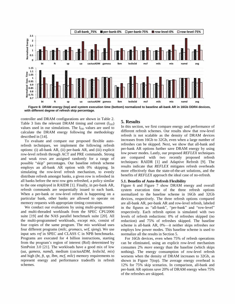
Figure 6 and Figure 7 show DRAM energy and overall
system execution time of the three refresh options
normalized to the baseline scheme in 16Gb and 32Gb
devices, respectively. The three refresh options compared
are all-bank AR, per-bank AR and row-level refresh, labeled
in the figures as “all-bank”, “per-bank” and “row-level”
respectively. Each refresh option is simulated with two
levels of refresh reductions: 0% of refreshes skipped (no
reduction) and 75% of refreshes skipped. The baseline
scheme is all-bank AR, 0%—it neither skips refreshes nor
employs low power modes. This baseline scheme is used to
normalize all the results in Section 5.
For 16Gb devices, even when 75% of refresh operations
can be eliminated, using an explicit row-level mechanism
consumes 2% more energy than the baseline (which skips
nothing). The energy consumption of row-level refresh
worsens when the density of DRAM increases to 32Gb, as
shown in Figure 7(top). The average energy overhead is
12% for 75% skip scenarios. In comparison, all-bank and
per-bank AR options save 20% of DRAM energy when 75%
of the refreshes are skipped.
Figure 6: DRAM energy (top) and system execution time (bottom) normalized to baseline all-bank AR in 16Gb DDR4 devices,
with different degree of refresh skip percentage.
0
0.5
1
1.5
2
2.5
bt ft sp ua cactusADM gamess lbm leslie3d mcf milc mix namd avg
No
rmal
ized
En
ergy
all-bank_75% per-bank-0% per-bank-75% row-level-0% row-level-75%
0.7
0.75
0.8
0.85
0.9
0.95
1
1.05
1.1
1.15
bt ft sp ua cactusADM gamess lbm leslie3d mcf milc mix namd avg
No
rmal
ized
Exe
c. T
ime

Performance improvement in 16Gb devices without skip
is similar for all the refresh options. However, as the number
of rows doubles in 32Gb devices, row-level refresh incurs a
30% performance degradation compared to the baseline.
The reason for this performance loss is that, when using
row-level refreshes, each bank stays mostly busy in
servicing refresh operations through ACT and PRE
commands, while leaving inadequate bandwidth for normal
memory requests. Further, when 75% of the refreshes are
skipped, all-bank, per-bank and row-level reduce execution
time by 8.1%, 9.5% and 7.5% respectively. Per-bank refresh
option shows better results as the number of refreshes
skipped is increased, especially in memory intensive
workloads such as lbm and mcf (18% and 12% respectively
when 75% refreshes are skipped).
Although row-level refresh sees performance benefits
from bank parallelism, the extra time required to finish
refreshes at a row granularity nullifies the bank parallelism
benefits as the number of rows increases in high density
devices. Hence, per-bank AR option is the right granularity
to utilize bank level parallelism rather than the row-level
option. As shown in our analysis, energy as well as
performance benefits by using only row-level refresh option
diminishes at higher DRAM densities, even when a large
fraction of refresh operations are skipped. In comparison,
our proposed REFLEX techniques provide scalable benefits
by serving most of refreshes through optimized all-bank and
per-bank AR options.
5.2. REFLEX with Low Power modes
Figure 8 presents energy and system execution time in 32Gb
devices when Power Down (PD) and Self-Refresh (SR)
modes are enabled. In the interest of space, only average
results of all the workloads are shown. In our
implementation, a rank switches to PD slow exit after the
request queue for that rank becomes empty, as proposed in
[22]. If a rank remains idle for a time period equal to tREFI,
then the rank switches to SR mode. AR options, both all-
bank and per-bank, are able to save background energy by
switching to low power modes in low activity periods. In
comparison, the row-level option reduces the opportunity to
stay in PD mode and is not compatible with SR mode.
Therefore, energy benefits of low power modes, quite
significant in workloads with medium to high idle periods
[23], are lost when row-level refreshes are employed.
Energy savings in all-bank and per-bank AR options
increase on average by 5-7% with low power modes. For
instance, in namd, all-bank AR exhibits 22% and 38%
DRAM energy improvement with PD and SR modes
respectively. Furthermore, since our proposed refresh
architecture provides the memory controller an ability to
access and synchronize the refresh counter before and after
SR mode, REFLEX techniques can be designed to reduce
unnecessary refreshes in SR mode by programming low
refresh rate, similar to the CO-FAST technique in [23]. Such
techniques could further reduce refresh energy in SR mode.
5.3. REFLEX versus Prior Schemes
In Figure 9, we compare recent refresh studies with different
implementations of our proposed REFLEX techniques.
REFLEX techniques assume a DRAM memory rank with
1K weak rows requiring refreshes in every 64ms, while rest
of the rows can be refreshed at 256ms period, an assumption
similar to the RAIDR study [1]. Our RAIDR
implementation skips 75% of refreshes, and schedules the
remaining 25% refreshes through row-level refresh option.
We also evaluate the recently proposed adaptive refresh
technique, which uses finer-granularity refresh modes
introduced in DDR4 [9]. Adaptive refresh decides
appropriate refresh granularity using a simple heuristic
Figure 7: DRAM energy (top) and system execution time (bottom) normalized to baseline all-bank AR in 32Gb DDR4 devices
0
1
2
3
4
bt ft sp ua cactusADM gamess lbm leslie3d mcf milc mix namd avg
No
rmal
ized
En
ergy
all-bank_75% per-bank-0% per-bank-75% row-level-0% row-level-75%
0.50.60.70.80.9
11.11.21.31.41.51.61.7
bt ft sp ua cactusADM gamess lbm leslie3d mcf milc mix namd avg
No
rmal
ized
Exe
c. T
ime

based on dynamically monitoring the serviced memory
bandwidth. Since adaptive refresh uses only all-bank AR
and does not reduce unnecessary refresh operations,
REFLEX techniques can coexist and provide more benefits.
Finally, we compare with an ideal case when DRAM is
not required to refresh at all. REFLEX techniques reach, on
average, within 6% of energy and 1% of performance as
compared to the ideal refresh case. When 75% of the refresh
operations are eliminated, the effective loss of bandwidth
due to refreshes decreases by a factor of 4. At that point,
refresh ceases to be a performance bottleneck. In
comparison, both RAIDR and Adaptive Refresh are unable
to close the gap with ideal, in particular for refresh energy
overheads, because RAIDR utilizes energy-inefficient row-
level option to reduce refresh whereas adaptive refresh does
not reduces unnecessary refreshes at all.
6. Other Related Work Flikker [24] and RAPID [25] are software techniques that
reduce unnecessary refreshes based on the distribution of
DRAM cell retention times. Flikker requires the program to
partition data into critical and non-critical sections. The
scheme issues refreshes at the regular rate for critical data
sections only, while non-critical sections are refreshed at
much slower rate. In RAPID, the retention time of a
physical page is known to the operating system, which
prioritizes the allocation of pages with longer retention time
over those with shorter retention time. However, as the
number of free pages decreases, the scheme does not
provide substantial benefits.
Elastic Refresh [26] and Coordinated Refresh [23] rely on
the ability to re-schedule refresh commands to overlap with
periods of DRAM inactivity. Elastic refresh postpones up to
eight refresh commands in high memory request phases of
programs, and then issues the pending refreshes during idle
memory phases at a faster rate to maintain the average
refresh rate. Coordinated Refresh techniques co-schedule
the refresh commands and the low power mode switching
such that most of the refreshes are energy efficiently issued
in SR mode. However, neither of these schemes reduces
unnecessary refresh operations.
Liu et al. [27] experimented with commodity DDR
devices to characterize retention periods. They showed that
the retention period of a given cell varies significantly with
time and temperature. Cui et al. [30] proposed a refresh
reduction mechanism which stores the retention time profile
in the DRAM itself to reduce storage overhead. They also
independently proposed the idea of silent refresh, which
bears some similarity to our dummy refresh command.
However, they did not provide any implementation details
or evaluation for silent refresh.
7. Conclusions We observe that since the refresh counter is controlled by
DRAM itself and is not visible to the memory controller,
refresh operations cannot be skipped with the default
JEDEC auto-refresh options in DDR SDRAMs. Further, our
analysis shows that the row-level refresh option used in
prior refresh reduction techniques is inefficient both in terms
of energy and performance. Therefore, the objective of our
work is to enable the coexistence of refresh reduction
techniques with the default auto-refresh mechanism so that
one could skip unneeded refreshes, while ensuring that the
required refreshes are serviced in an energy-efficient
manner.
We have proposed simple and practical modifications in
DRAM refresh architecture to enable the memory controller
to read, write and increment the refresh counter in a DRAM
device. This new architecture enables the memory controller
to skip refresh operations by only incrementing the refresh
counter. We have also proposed flexible auto-refresh
(REFLEX) techniques that reduce as many refreshes as prior
row-level only refresh schemes, while serving remaining
refreshes efficiently through the existing auto-refresh
option. As the energy and performance overheads of refresh
operations become significant in high density memory
systems, the increasing advantages of our proposed
techniques make a strong case for the small modifications in
DRAM device to access the refresh counter.
Acknowledgements The authors would like to thank David Wang, Mu-Tien
Chang, and the anonymous reviewers for their valuable
inputs. The research was funded in part by Intel Corporate
Research Council’s University Research Office, the United
State Department of Energy, Sandia National Laboratories,
and the United States Department of Defense.
Figure 9: Comparison with other refresh schemes
00.10.20.30.40.50.60.70.80.9
11.11.2
Normalized Energy Normalized Exec. Time
No
rmal
ize
to b
asel
ine
AR
baseline REFLEX_1x REFLEX_4x REFLEX_rowREFLEX_bank RAIDR Adaptive No_Refresh
Figure 8: Energy and performance in low power modes
0
0.25
0.5
0.75
1
1.25
1.5
1.75
2
2.25
2.5
Energy (PD) Exec. Time(PD) Energy (PD+SR) Exec. Time(PD+SR)
No
rmal
ize
d t
o A
R w
ith
ou
t
low
po
wer
mo
des
all-bank-0% all-bank_50% all-bank_75%
per-bank-0% per-bank-50% per-bank-75%
row-level-0% row-level-50% row-level-75%

References
[1] J. Liu, B. Jaiyen, R. Veras, and O. Mutlu, “RAIDR: Retention-
aware intelligent DRAM refresh,” 2012 39th Annual International Symposium on Computer Architecture (ISCA), pp.
1–12, Jun. 2012.
[2] M. Ghosh and H.-H. S. Lee, “Smart Refresh: An Enhanced Memory Controller Design for Reducing Energy in Conventional
and 3D Die-Stacked DRAMs,” 40th Annual IEEE/ACM
International Symposium on Microarchitecture MICRO 2007, pp. 134–145, 2007.
[3] C. Isen and L. John, “ESKIMO - Energy Savings using Semantic
Knowledge of Inconsequential Memory Occupancy for DRAM subsystem,” in Proceedings of the 42nd Annual IEEE/ACM
International Symposium on Microarchitecture, 2009, pp. 337–
346.
[4] T. Hamamoto, S. Sugiura, and S. Sawada, “On the retention time
distribution of dynamic random access memory (DRAM),” IEEE
Transactions on Electron Devices, vol. 45, no. 6, pp. 1300–1309, Jun. 1998.
[5] K. Kim and J. Lee, “A New Investigation of Data Retention Time
in Truly Nanoscaled DRAMs,” IEEE Electron Device Letters, vol. 30, no. 8, pp. 846–848, Aug. 2009.
[6] T. Ohsawa, K. Kai, and K. Murakami, “Optimizing the DRAM
Refresh Count for Merged DRAM/Logic LSIs,” in ISLPED,1998, 1998, pp. 82–87.
[7] JEDEC, “DDR4 STANDARD,” 2012.
[8] B. Jacob, S. W. Ng, and D. T. Wang, “Memory Systems: Cache,
DRAM, Disk.”Morgan Kaufmann, ISBN 978-0123797513, 2007.
[9] J. Mukundan, H. Hunter, K. Kim, and J. Stuecheli, “Understanding and Mitigating Refresh Overheads in High-
Density DDR4 DRAM Systems,” in ISCA, 2013.
[10] JEDEC, “Low Power Double Data Rate 3,” 2012.
[11] J. Liu, B. Jaiyen, Y. Kim, C. Wilkerson, and O. Mutlu, “An
experimental study of data retention behavior in modern DRAM
devices,” Proceedings of the 40th Annual International Symposium on Computer Architecture - ISCA ’13, p. 60, 2013.
[12] Micron Technology, “Various Methods of DRAM Refresh,”
1999.
[13] Y. Kim, V. Seshadri, D. Lee, J. Liu, and O. Mutlu, “A case for
exploiting subarray-level parallelism (SALP) in DRAM,” in
ISCA, 2012, vol. 40, no. 3, p. 368.
[14] Micron Technology, “Calculating Memory System Power for
DDR3,” 2007.
[15] K. K. Chang, D. Lee, Z. Chishti, A. R. Alameldeen, C. Wilkerson, Y. Kim, and O. Mutlu, “Improving DRAM
Performance by Parallelizing Refreshes with Accesses,” in
HPCA, 2014.
[16] Micron Technology, “4Gb Mobile LPDDR2 SDRAM,” 2011.
[17] A. Patel, F. Afram, S. Chen, and K. Ghose, “MARSS: a full
system simulator for multicore x86 CPUs,” in Proceedings of the 48th Design Automation Conference, 2011.
[18] P. Rosenfeld, E. Cooper-Balis, and B. Jacob, “DRAMSim2: A
Cycle Accurate Memory System Simulator,” Computer Architecture Letters, 2011.
[19] J. L. Henning, “SPEC CPU2006 benchmark descriptions,”
SIGARCH Comput. Archit. News.
[20] NASA, “NAS Parallel Benchmarks (NPB 3.3.1).”
[21] G. Hamerly, E. Perelman, J. Lau, and B. Calder, “Simpoint 3.0: Faster and more flexible program phase analysis,” Journal Of
Instruction Level Parallelism, vol. 7, no. 4, pp. 1–28, 2005.
[22] I. Hur and C. Lin, “A comprehensive approach to DRAM power management,” 2008 IEEE 14th International Symposium on High
Performance Computer Architecture, pp. 305–316, 2008.
[23] I. Bhati, Z. Chishti, and B. Jacob, “Coordinated Refresh : Energy Efficient Techniques for DRAM Refresh Scheduling,” in
ISLPED, 2013.
[24] S. Liu, K. Pattabiraman, T. Moscibroda, and B. G. Zorn, “Flikker: saving DRAM refresh-power through critical data
partitioning,” in Proceedings of the sixteenth international
conference on Architectural support for programming languages and operating systems, 2011, pp. 213–224.
[25] R. K. Venkatesan, S. Herr, and E. Rotenberg, “Retention-Aware
Placement in DRAM (RAPID): Software Methods for Quasi-
Non-Volatile DRAM,” in The Twelfth International Symposium
on High Performance Computer Architecture 2006, 2006, pp.
157–167.
[26] J. Stuecheli, D. Kaseridis, H. C Hunter, and L. K. John, “Elastic
Refresh: Techniques to Mitigate Refresh Penalties in High
Density Memory,” 2010 43rd Annual IEEE/ACM International Symposium on Microarchitecture, pp. 375–384, 2010.
[27] J. Liu, B. Jaiyen, Y. Kim, and C. Wilkerson, “An Experimental
Study of Data Retention Behavior in Modern DRAM Devices : Implications for Retention Time Profiling Mechanisms,” in ISCA,
2013.
[28] S. Rixner, W. J. Dally, U. J. Kapasi, P. Mattson, and J. D. Owens,
“Memory access scheduling,” in Proceedings of the 27th annual
international symposium on Computer architecture - ISCA ’00, 2000, pp. 128–138.
[29] Samira Khan, Donghyuk Lee, Yoongu Kim, Alaa Alameldeen,
Chris Wilkerson, and Onur Mutlu, "The efficacy of error mitigation techniques for DRAM retention failures: a comparative
experimental study," in The 2014 ACM international conference
on Measurement and modeling of computer systems, SIGMETRICS, 2014.
[30] Zehan Cui, Sally A. McKee, Zhongbin Zha, Yungang Bao, and
Mingyu Chen, "DTail: a flexible approach to DRAM refresh management," In Proceedings of the 28th ACM international
conference on Supercomputing (ICS '14). ACM, New York, NY,
USA, 2014.