Approaches to Scaling.” Integrated Microelectronic Devices Fall 2002 Lecture 301 ... 0.7 1 Fig....
21
6.720J/3.43J Integrated Microelectronic Devices Fall 2002 Lecture 301 Lecture 30 The ”Short” MetalOxideSemiconductor FieldEffect Transistor November 15, 2002 Contents: 1. Shortchannel effects Reading assignment: P. K. Ko, ”Approaches to Scaling.”
Transcript of Approaches to Scaling.” Integrated Microelectronic Devices Fall 2002 Lecture 301 ... 0.7 1 Fig....

6.720J/3.43J Integrated Microelectronic Devices Fall 2002 Lecture 301
Lecture 30 The ”Short”MetalOxideSemiconductor FieldEffect
Transistor
November 15, 2002
Contents:
1. Shortchannel effects
Reading assignment:
P. K. Ko, ”Approaches to Scaling.”

6.720J/3.43J Integrated Microelectronic Devices Fall 2002 Lecture 302
Key questions
• Why does it seem that in practice the drain current is signifi
cantly smaller than predicted by simple long MOSFET models?
• What is the impact of velocity saturation in the device charac
teristics?

6.720J/3.43J Integrated Microelectronic Devices Fall 2002 Lecture 303
1. Shortchannel effects
� Mobility degradation: mobility dependence on Ex (vertical
field).
Experimental observation in linear regime:
VGS
ID
Vth
small VDS
0 0 VGS
gm
Vth
small VDS
0 0
Experimental observation:
µo
νµeff =
1 + |Eav |Eo
where Eav is average normal field in inversion layer:
Qdmax + 12QiEav =
�s
Due to semiconductoroxide interface roughness.

6.720J/3.43J Integrated Microelectronic Devices Fall 2002 Lecture 304
µeff vs. Eav: universal relationship for many MOSFET designs:
Parameters for the effective mobility models for electrons and holes:
electrons
µo (cm2/V · s) 670
Eo (MV/cm) 0.67
ν 1.6
holes
160
0.7
1
Fig. 4. Measured universal µeff vs. Eeff curves for electrons and holes in the inversion layer.(After Liang et al. [20].)

6.720J/3.43J Integrated Microelectronic Devices Fall 2002 Lecture 305
Figure 6 graph from Inversion layer electron mobility data, graph from: Arora and Richardson, P. Ko,"Approaches to Scaling," in VLSI Electronics: Microstructure Science, vol. 18, chapter 1, pp. 1--37, Academic Press, 1989.

6.720J/3.43J Integrated Microelectronic Devices Fall 2002 Lecture 306
Simplified expression of Eav for n+polySi gate:
1) Relationship between Qdmax and Vth:
Vth = VFB + φsth −Qdmax
Cox
with:
1 1 1EgVFB = −φbi = (WM−WS) = (WM−χs−
Eg−qφf) = −q 2
−φf q q 2
Plug into Vth and solve for Qdmax:
Qdmax = −Cox(Vth+ Eg
+φf−2φf) = −Cox(Vth+ Eg−φf) � −CoxVth
2q 2q
2) Relationship between Qi and VGS − Vth:
Qi = −Cox(VGS − Vth)
3) Plug Qdmax and Qi into Eav:
1 1
|Eav| � |Qdmax + 2Qi | =
CoxVth + 2Cox(VGS − Vth) �ox VGS + Vth
= �s �s �s 2xox

6.720J/3.43J Integrated Microelectronic Devices Fall 2002 Lecture 307
|Eav| � �ox VGS + Vth
�s 2xox
Key dependences:
• VGS ↑⇒ |Eav| ↑⇒ µeff ↓
• Vth ↑⇒ |Eav| ↑⇒ µeff ↓
• xox ↓⇒ |Eav| ↑⇒ µeff ↓
Fig. 5. Calculated µeff of current carrier, graph. From: VLSI Electronics P. Ko,"Approaches to Scaling," in VLSI Electronics: Microstructure Science, vol. 18, chapter 1, pp. 1--37, Academic Press, 1989.

6.720J/3.43J Integrated Microelectronic Devices Fall 2002 Lecture 308
Several comments:
• Since ID ∼ µe, mobility degradation more severe as VGS in
creases ⇒ ID won’t rise as fast with VGS.
• Since µe depends on |Eav| ⇒ µeff depends on y. Disregard to
first order ⇒ use same µeff everywhere.
• Mobility degradation considered ”shortchannel effect” because
as L ↓⇒ xox ↓ and µ degradation becomes important.
6.720J/3.43J Integrated Microelectronic Devices Fall 2002 Lecture 309
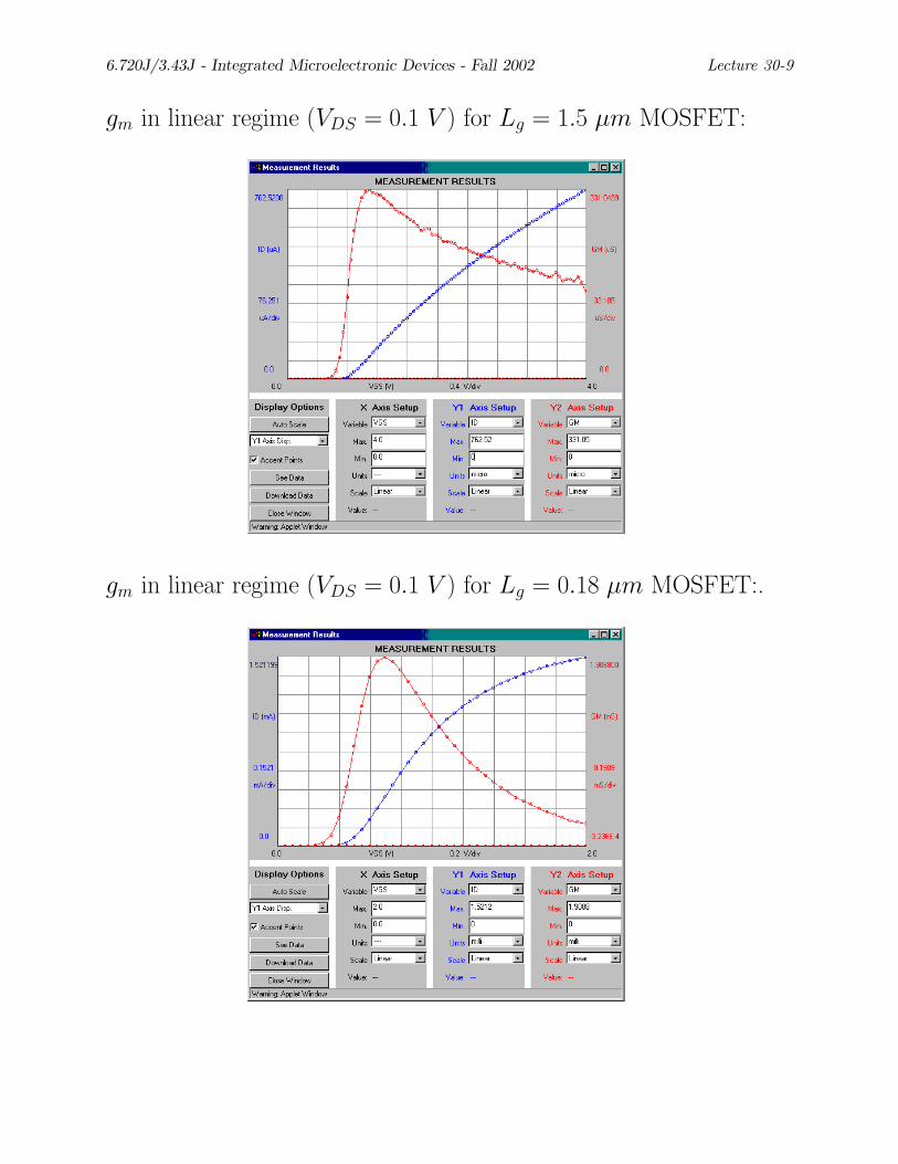
gm in linear regime (VDS = 0.1 V ) for Lg = 1.5 µm MOSFET:
gm in linear regime (VDS = 0.1 V ) for Lg = 0.18 µm MOSFET:

6.720J/3.43J Integrated Microelectronic Devices Fall 2002 Lecture 3010
� Velocity saturation
At high longitudinal fields, ve cannot exceed vsat:
vdrift
vsat
0 µ
ε0 εsat
Best fit to experiments:
µeE ve =
(1 + |µeE |n)1/nvsat
For inversion layer:
electrons holes
vsat (cm/s) 8 × 106 cm/s 6 × 106 cm/s
n 2 1
To develop analytical model, use n = 1:
µeE ve =
1 + |µeE |vsat
6.720J/3.43J Integrated Microelectronic Devices Fall 2002 Lecture 3011
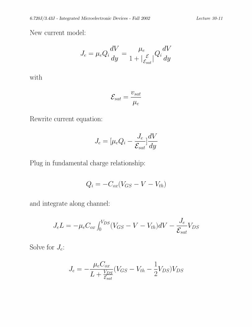
New current model:
dVJe = µeQi
dy =
µe dV
1 + | E Esat
|Qi
dy
with
Esat = vsat
µe
Rewrite current equation:
Je = [µeQi − Je ]dV
Esat dy
Plug in fundamental charge relationship:
Qi = −Cox(VGS − V − Vth)
and integrate along channel:
JeJeL = −µeCox
� VDS (VGS − V − Vth)dV −Esat
VDS0
Solve for Je:
1Je = − µeCox
VDS (VGS − Vth −
2VDS)VDS
L + Esat

6.720J/3.43J Integrated Microelectronic Devices Fall 2002 Lecture 3012
Terminal drain current in linear regime:
W µeCox 1ID =
L 1 + VDS (VGS − Vth −
2VDS)VDS
EsatL
Effectively, impact of velocity saturation:
µe µe ⇒
1 + VDS EsatL
with VDS ≡ average longitudinal field.L
• For VDS � Esat ⇒ velocity saturation irrelevant (mobility regime).L
• For VDS � Esat ⇒ velocity saturation prominent (velocity satL
uration regime).
Since Esat � 105 V/cm and VDS order 1− 10 V , velocity saturation
important if L ∼ 0.1 − 1 µm.

6.720J/3.43J Integrated Microelectronic Devices Fall 2002 Lecture 3013
Current saturation occurs when vsat reached anywhere in the channel
⇒ ID won’t increase anymore with VDS:
p
n+n+
n+
v=vsat ε=εsat V=VDSsat ID=IDsat
Bottleneck is current flowing through vsat region:
IDsat = −WveQi
= WvsatCox(VGS − Vth − VDSsat)
W µeCox 1 =
L 1 + VDSsat (VGS − Vth − VDSsat)VDSsat
2EsatL
Solve for VDSsat:
VDSsat = EsatL(
�����1 + 2VGS − Vth
EsatL− 1)

�
6.720J/3.43J Integrated Microelectronic Devices Fall 2002 Lecture 3014
VGS − VthVDSsat = EsatL( 1 + 2
�����EsatL
− 1)
• For long L, VDSsat � VGS − Vth
• For short L, VDSsat � 2EsatL(VGS − Vth) < VGS − Vth
VDSsat
0
mobility � regime
velocity saturation � regime
0 VGS-Vth
Velocity saturation results in premature current saturation and less
current:
IDsat = WvsatCox(VGS − Vth − VDSsat)

6.720J/3.43J Integrated Microelectronic Devices Fall 2002 Lecture 3015
Experiments:
Fig. 7. The saturation voltage for several channel lengths, graph. From: VLSI P. Ko, "Approaches to Scaling," in VLSI Electronics: Microstructure Science, vol. 18, chapter 1, pp. 1--37, Academic Press, 1989.

6.720J/3.43J Integrated Microelectronic Devices Fall 2002 Lecture 3016
Currentvoltage characteristics:
Fig. 15 Comparison of drain characteristics for constant mobility case and P. Ko, "Approaches to Scaling," in VLSI Electronics: Microstructure Science, vol. 18, chapter 1, pp. 1--37, Academic Press, 1989.

6.720J/3.43J Integrated Microelectronic Devices Fall 2002 Lecture 3017
Impact of velocity saturation on transconductance:
∂IDsat gm = = WvsatCox(1 − ∂VDSsat
)∂VGS ∂VGS
with
∂VDSsat 1 = �
∂VGS 1 + 2VGS−Vth EsatL
Then:
1 gm = WvsatCox(1 − � )
1 + 2VGS−Vth EsatL
In the limit of short L:
gm = WvsatCox
In the limit of short L, gm determined only by xox.

6.720J/3.43J Integrated Microelectronic Devices Fall 2002 Lecture 3018
theoretical � limit for L=0
Fig. 10: Deep submicon NMOS transistors, graph. From: VLSI Electronics P. Ko, "Approaches to Scaling," in VLSI Electronics: Microstructure Science, vol. 18, chapter 1, pp. 1--37, Academic Press, 1989.

6.720J/3.43J Integrated Microelectronic Devices Fall 2002 Lecture 3019
L=1 µm, xox=20 nm
L=2 µm, xox=30 nm
L=3 µm, xox=50 nm
L=1.3 µm, xox=20 nm
L=2.3 µm, xox=30 nm
L=3.3 µm, xox=50 nm
Fig. 9: Measured and calculated gm, graph. From: VLSI Electronics Microstructure P. Ko, "Approaches to Scaling," in VLSI Electronics: Microstructure Science, vol. 18, chapter 1, pp. 1--37, Academic Press, 1989.
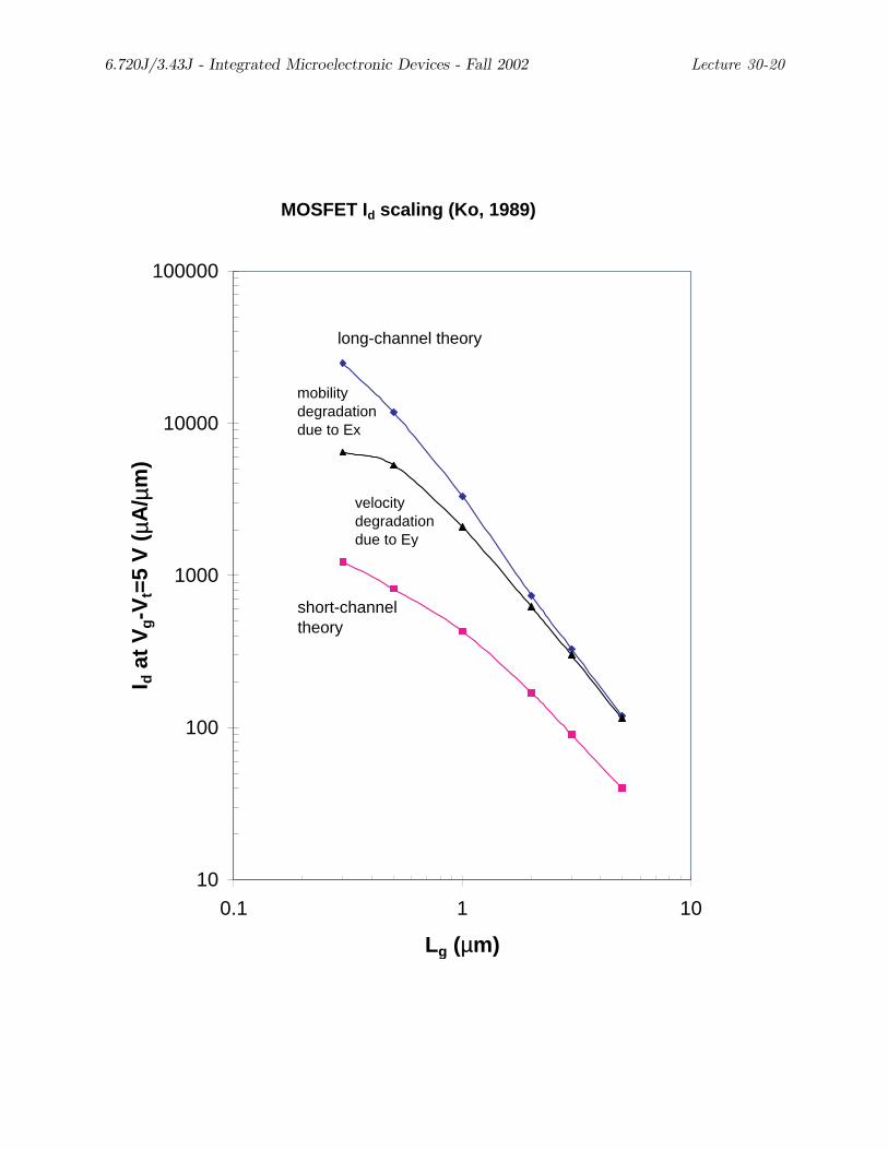
6.720J/3.43J Integrated Microelectronic Devices Fall 2002 Lecture 3020
MOSFET Id scaling (Ko, 1989)
100000
10000
1000
100
10
I d a
t V
g-V
t =5
V (
µµA/ µµ
m)
long-channel theory
short-channel theory
velocity degradation due to Ey
mobility degradation due to Ex
0.1 1 10
Lg (µµm)

6.720J/3.43J Integrated Microelectronic Devices Fall 2002 Lecture 3021
Key conclusions
• Inversion layer mobility degraded by transveral field due to rough
ness of semiconductoroxide interface ⇒ ID lower than predicted
by simple models.
• There is a universal relationship between mobility and average
transversal field in inversion layer.
• For short L, velocity saturation in inversion layer important ⇒ ID lower than predicted by simple models.
• Velocity saturation ⇒ premature MOSFET saturation ⇒ VDSsat
lower than predicted by simple models.
• Velocity saturation ⇒ gm saturation in limit of short L:
gm = WvsatCox