Application of the TDA6120 wideband video output amplifier...
71
APPLICATION NOTE Application of the TDA6120 wideband video output amplifier AN96073 Philips Semiconductors
Transcript of Application of the TDA6120 wideband video output amplifier...

APPLICATION NOTE
Application of theTDA6120 wideband
video output amplifierAN96073
PhilipsSemiconductors

Philips Semiconductors___________________________________________________________________TDA6120Q Application NoteWideband video output amplifier AN96073
-2-
Abstract
This report gives a description of the TDA6120Q wideband video output amplifier together withapplication aspects
© Philips Electronics N.V. 1997
All rights are reserved. Reproduction in whole or in part is prohibited without the prior written consent of thecopyright owner. The information presented in this document does not form part of any quotation or contract, isbelieved to be accurate and reliable and may be changed without notice. No liability will be accepted by the publisherfor any consequence of its use. Publication thereof does not convey nor imply any license under patent- or otherindustrial or intellectual property rights.

Philips Semiconductors___________________________________________________________________TDA6120Q Application NoteWideband video output amplifier AN96073
-3-
Application of theTDA6120Q wideband
Video output amplifierAN96073
Author(s):
E.H. SchutteDesign & Application Video Group, Consumer IC's Nijmegen,
The Netherlands
Keywords
Video amplifierRise & FalltimeFlash-protection
Dissipation
Date: 15th July, 1997

Philips Semiconductors___________________________________________________________________TDA6120Q Application NoteWideband video output amplifier AN96073
-4-
Summary
This note gives the device description of the TDA6120Q RGB wideband video outputamplifier and provides the user with basic hints to obtain an optimal performance inthe application.The TDA6120Q includes one video output amplifier (30MHz/125Vpp) in a plastic DIL-bent -SIL power package DBS13P, using high-voltage DMOS technology, and isintended to drive the cathodes of a CRT in a high demanding market of HighResolution TVs and monitors. The device is provided with a black currentmeasurement output for automatic black current stabilisation (ABS).
The following application aspects will be described:• External components calculation.• Circuit application & Application hints.• Flash-over protection.
Furthermore two wideband concepts are described within this report.
• One video concept for typical TV applications, using the combinationTDA4780 (monolithic RGB processor ) and the TDA6120Q.This combination has a total bandwidth of 22MHz and is suitable for High ResolutionTV,MUSE and VGA (SVGA with limites bandwidth performance ).It features gamma and blue stretch and has automatic black current stabilisation(ABS).
• The other concept is designed for monitor applications, using the combination ofTDA4882 monitor pre-amplifier and the TDA6120Q .This combination has a total bandwidth of 30-60 MHz ( depending on the cathodeoutput swing requirement and is suitable for VGA, SVGA and XGA applications.
By means of this application note one is able to decide which components can bechanged and what the consequences will be. This is important because thecomponent choice is often a compromise and depends on the requirements definedby the customer.
Philips Semiconductors___________________________________________________________________TDA6120Q Application NoteWideband video output amplifier AN96073
-5-
TABLE OF CONTENTS:
1.0 INTRODUCTION…………………………………………………………………… 7
2.0 QUICK REFERENCE DATA……………………………………………………… 8
3.0 CIRCUIT DESCRIPTION…………………………………………………………. 10- 3.1 Block diagram description………………………………………………. 10- 3.2 Functional pin description………………………………………………. 12- 3.3 Internal pin configuration………………………………………………. 13- 3.4 Protection circuits………………………………………………………... 13
4.0 DESIGN CONSIDERATIONS……………………………………………………. 14- 4.1 Basic aspects amplifier part……………………………………………. 14- 4.2 Voltage gain……………………………………………………………… 15- 4.3 DC to DC transfer………………………………………………………... 15- 4.4 Pole zero cancellation…………………………………………………... 15- 4.5 Stability……………………………………………………………………. 16- 4.6 Black current measurement output…............................................... 16- 4.7 Flash-over protection...............................................................…..... 16
5.0 EXTERNAL COMPONENTS CALCULATION……..........................……...... 17- 5.1 Feedback resistor.............…..............................................…........... 17- 5.2 Input resistor.......................….................................................…….. 17- 5.3 Speed-up capacitor........…......................................................…..... 18- 5.4 Reference voltage ..................................................................…….. 18- 5.5 Vdd & Vcc decoupling...........…...............................................…..... 18- 5.6 Decoupling recarding flash........……................................................ 19- 5.7 Flash diodes.............................................................................….... 19- 5.8 Additional components................…................................................. 20
6.0 DISSIPATION & HEATSINK CALCULATION……..............................…....... 21- 6.1 Static and dynamic dissipation…….......................................…….... 21- 6.2 Heatsink calculation………............................................................... 22- 6.3 Absolute worst case conditions…...…….......................................... 22- 6.4 A more practical approach regarding dissipation……...............…… 23
7.0 CIRCUIT APPLICATION & APPLICATION HINTS………............................ 24• Application diagram of the TDA6120Q……......….….............................. 38• Partlist…..........................................................….…............................... 39• Evaluation board layout & component view………................................. 40- 7.1 Design-in sequence of the TDA6120Q........………….….................. 24- 7.2 Printed circuit board.............................................………….............. 24- 7.3 Cross-talk..............................................................................………. 26- 7.4 Switch off behaviour.................................................................……. 27- 7.6 Flash- over protection..............................................…..............…… 30
- 7.7 Black- current stabilisation.......................................................……. 33

Philips Semiconductors___________________________________________________________________TDA6120Q Application NoteWideband video output amplifier AN96073
-6-
8.0 PERFORMANCE EVALUATION......................................................………... 34- 8.1 Bandwidth........................................................................................ 34- 8.2 Multi-burst performance................................................................... 34- 8.3 Cross-talk......................................................................................... 35- 8.4 Rise and Fall time............................................................................. 35- 8.5 Flash test.......................................................................................... 35
9.0 ACKNOWLEDGMENT................................................................................... 37
10.0 REFERENCES........................................................................................... 37
11.0 APPENDIX
- Imperfections of the TDA6120Q..…….................................................... 49
-"Passive" interface add-on board.......…….............................................. 50
- TDA4882 add-on board............................……....................................... 54
- TDA4780 add-on board.................................…..................................... 62

Philips Semiconductors___________________________________________________________________TDA6120Q Application NoteWideband video output amplifier AN96073
-7-
1.0 INTRODUCTION The aim of this application note is to describe the basic operation of the TDA6120Q Wideband RGB video output amplifier and provide the user with basic hints to realise anoptimal performance in the application.The TDA6120Q includes one video output amplifiers in a plastic DIL-bent -SIL powerpackage DBS13P, using high-voltage DMOS technology, and is intended to drive of a CRT ina high demanding market of High Resolution TVs and monitors.The device is provided with a black current measurement output for automatic black currentstabilisation (ABS).The TDA6120Q does not include flash protection diodes, therefore it is necessary to apply anexternal flash diode for each channel.
Two video output concepts are described in this report.• One video concept concept for typical TV applications, using the combinationTDA4780 [(monolithic RGB processor ) add-on board ] and the TDA6120Q[ main board]. This combination has a total bandwidth of 22MHz and is suitable for TV,MUSEand VGA (SVGA with limited bandwidth performance ) .It features gamma and blue stretch and has automatic black current stabilisation (ABS).With this concept there are no alignments any more on the CRT panel, because of theautomatic black current stabilisation and because the white point adjustment can be done inthe TDA4780 via I2C bus.
• The other concept is designed for monitor applications, using the combination TDA4882monitor pre-amplifier (add-on board) and the TDA6120Q (mainCRTboard).This combination has a total RGB bandwidth of 30-60 MHz ( depending on the cathodeoutput swing requirement and is suitable for VGA, SVGA and XGA applications.
The main features are:• High large signal bandwidth : 40 MHz typ at 100Vpp, 1)• High slewrate : 10V / ns,• differential voltage input,• Black-current measurement output for automatic black current stabilization,• Bandwidth indepent of voltage gain,• High power supply rejection ratio,• Protection against ESD,• Low static power dissipation,• Controllable switch-off behaviour.
1) Measured in application set-up, with Rfl =220Ω and Cl= Ctube+ Cpcb=10pF.
Philips Semiconductors___________________________________________________________________TDA6120Q Application NoteWideband video output amplifier AN96073
-8-
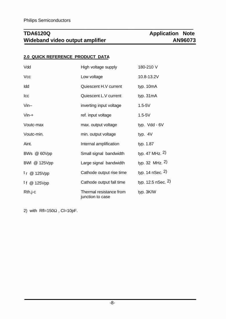
2.0 QUICK REFERENCE PRODUCT DATA
Vdd
Vcc
High voltage supply
Low voltage
180-210 V
10.8-13.2V
Idd
Icc
Quiescent H.V current
Quiescent L.V current
typ. 10mA
typ. 31mA
Vin--
Vin-+
Voutc-max
inverting input voltage
ref. input voltage
max. output voltage
1.5-5V
1.5-5V
typ. Vdd - 6V
Voutc-min. min. output voltage typ. 4V
Aint. Internal amplification typ. 1.87
BWs @ 60Vpp Small signal bandwidth typ. 47 MHz. 2)
BWl @ 125Vpp Large signal bandwidth typ. 32 MHz. 2)
t r @ 125Vpp Cathode output rise time typ. 14 nSec. 2)
t f @ 125Vpp Cathode output fall time typ. 12.5 nSec. 2)
Rth,j-c Thermal resistance fromjunction to case
typ. 3K/W
2) with Rfl=150Ω , Cl=10pF.

Philips Semiconductors___________________________________________________________________TDA6120Q Application NoteWideband video output amplifier AN96073
-9-
1)Rf=22kΩ Ri=450Ω
2)Rf=11kΩ Ri=450Ω
3)Rf=22kΩ Ri=900Ω
Vin+ =3V
Fig.1 DC to DC transfer from input (Vin-) to output (Voutc)
SYMBOL PIN DESCRIPTION
RC- 1 Inverting input pre-emphasisnetwork
VIN- 2 Inverting voltage inputRC+ 3 Non-inverting input pre- emphasis
networkVIN+ 4 Non-inverting voltage inputIIN 5 Feedback current inputVCC 6 Low supply voltage ( 12V )
OUTM 7 Cathode current measurementoutput
GND 8 Power groundn.c. 9 Not connected
VDD 10 High supply voltage ( 200V )n.c. 11 Not connectedOUTC 12 Cathode output
OUT 13 Feedback output
Fig.2 Pinconfiguration
VINN[V]
VO
UT
C[V
]
020406080
100120140160180200
0 1 2 3 4 5 6
RC−
VIN−
RC+
VIN+
IIN
VCC
OUTM
GND
n.c.
VDD
n.c.
OUTC
OUT
1
2
3
4
5
6
7
8
9
10
11
12
13
TDA6120Q
MGK438

Philips Semiconductors___________________________________________________________________TDA6120Q Application NoteWideband video output amplifier AN96073
-10-
3.0 CIRCUIT DESCRIPTION.3.1 BLOCK DIAGRAM DESCRIPTION.The complete block diagram of the TDA6120Q is shown in Fig. 3.
Fig.3 Block diagram of the TDA6120Q.
The TDA6120Q consists of one monolithic video output amplifier.The amplifier can be split-up in two amplifier stages in series. The first one is a voltage tocurrent stage (transadmittance stage), the second one is a current to voltagestage(transimpedance stage).This gives rise to the term transadmittance - transimpedance amplifier.At the second stage voltage to current feedback is applied by a resistor connectedfrom OUT(pin13 ) to Iin(pin5). The transadmittance of the first stage can be chosen by meansof a resistor between pin1 and pin3.The advantage of this amplifier configuration is that a higher bandwidth performance can berealised w.r.t the well known operational amplifier with voltage feedback.Furthermore, the amplifier has a differential input, which makes the amplifier less sensitive forinjection from noise sources and flexible regarding DC to DC transfer.The TDA6120Q does not include flash protection diodes that clamp the cathode output to thehigh voltage supply pin during a CTR flashover discharge.Therefore an external flash diode combined with flash resistor and sparkgap has to protectthe amplifiers against flash over in the picture tube.Furthermore, the device needs two supply voltages, a low supply voltage(Vcc) of 12V and ahigh supply voltage(Vdd) of 200V.
MGK440
1×
1 ×
CURRENT INPUT
out 1 ×
in
out 4 ×
MIRR OR×in out
CASCODEMIRROR4×in out
CASCODE+
J 5 mA
0.7 pF
TDA6120Q
9, 11
6
2
n.c.
VCC
VIN −
1 3 4
R C − R C + VIN +
8
G N D
12
13
7
OUTC
O U T
OUTM
IIN VD D
105

Philips Semiconductors___________________________________________________________________TDA6120Q Application NoteWideband video output amplifier AN96073
-11-
The TDA6120Q is provided with a black current data pin. When using TDA4780 as drivedevice no adjustments are required for gain and black setting, as the TDA4780 has I2Cwhite point adjustment and black current input pin.The simplified basic application diagram of theTDA6120Q is given below in Fig.4The complete application diagram of theTDA6120Q is given in Fig.18 on page 38.
Fig. 4 Simplified basic application of the TDA6120Q.
MGK441
442 Ω
68 pFC1
RC − RC +
1 3 5 7 9 11 13
2 4 6 8 10 12
22 Ω
VIN − VIN +
C r10 nF
CCC47µF
C DD10µ F
C C100nF
C D100nF
TDA6120Q
22 k Ω
R f
IIN OUTM n.c. n.c. OUT
CRTVIN220 Ω
50 Ω
R flash
VCC VDD
Dflash
OUTCGND
+12 V +200 VV ref
R ia
R i

Philips Semiconductors___________________________________________________________________TDA6120Q Application NoteWideband video output amplifier AN96073
-12-
3.2 FUNCTIONAL PIN DESCRIPTION.A functional pin description is given in this chapter.Pin1,3 . These are the inverting and non-inverting pre-emphasis pins.A resistor/capacitor network has to be connected between these pins for gain andpre- emphasis setting.
Pin 2. This is the inverting voltage input. The input configuration consist of a bipolar npntransistor in a long tailed pair configuration. The input current amounts to30 µA.typ.The input voltage range amounts to 1.5<Vin-<5V.
Pin 4. This is the non-inverting (ref.) voltage input. The input configuration consist of abipolar npn transistor in a long tailed pair configuration. The input current amounts to30µA.typ. The input voltage range amounts to 1.5<Vin-<5V.
Pin 5. Feedback current input.A feedback resistor (Rf) has to be connected from the feedback output (pin13) to this pin.The DC level at this pin is defined by 2Vbe.
Pin6. Low voltage supply.This pin has to be decoupled by a h.f and l.f decoupling capacitor.
Pin 7. This is the black current measurement output for automatic black current stabilisation(ABS). The voltage on pin 7 of the TDA6120Q is limited by an internal built in zener diode of20 volts. The off-set current of pin5 amounts to +20 µA typ. at 4V< Vom< 20V. When notusing ABS, this pin can be grounded via a capacitor.
Pin8. Ground
Pin9,11. Not connected
Pin 10. High-voltage supply Vdd.This is the high voltage supply pin of the device(typ.200V) and has to be decoupled .
Pin 12. Cathode output.The video output current is delivered by a quasi complementary class-A/B push-pull stage,designed in DMOS technology and can source and sink a current of 100 mA, for video outputvoltages of 125Vp-p with rise and fall times of 12.5 nSec .A feature of this output stage is the low saturation voltage (typ. 4V ) and the low voltage dropat high level (typ.Vdd-6V).This output pin has to be connected to the cathode of the CRT via a standard resistor of 50Ωand a high-voltage flash-over protection resistor.A high surge clamping diode has to be applied externally between this OUTC pin and theVdd pin, so that the cathode output voltage clamps to Vdd+Vdiode.
pin13. Feedback output.This output is used for feedback to the current input (pin5) by means of resistor (Rf) .

Philips Semiconductors___________________________________________________________________TDA6120Q Application NoteWideband video output amplifier AN96073
-13-
3.3 INTERNAL PIN CONFIGURATIONThe internal pin configuration of the TDA6120Q is given in Fig 5.
Fig. 5 Internal pin configurations of the TDA6120Q
3.4 PROTECTION CIRCUITS.The TDA6120Q has a lot of protection circuits built-in, in order to comply with requirements ofreliability.
• Protection against electrostatic discharges. All pins have an energy protection for positive and negative voltages.
MGK439
ESD
ESD
ESD
ESD
TDA6120Q
7
8
12
106
ESD
ESD
13
2
1
ESD
ESD
ESD
4
3
ESD
5
RC+
VIN+
RC− OUTC
VDDVCC
OUT
OUTM
GND
VIN −
IIN
Philips Semiconductors___________________________________________________________________TDA6120Q Application NoteWideband video output amplifier AN96073
-14-
4.0 DESIGN CONSIDERATIONS.
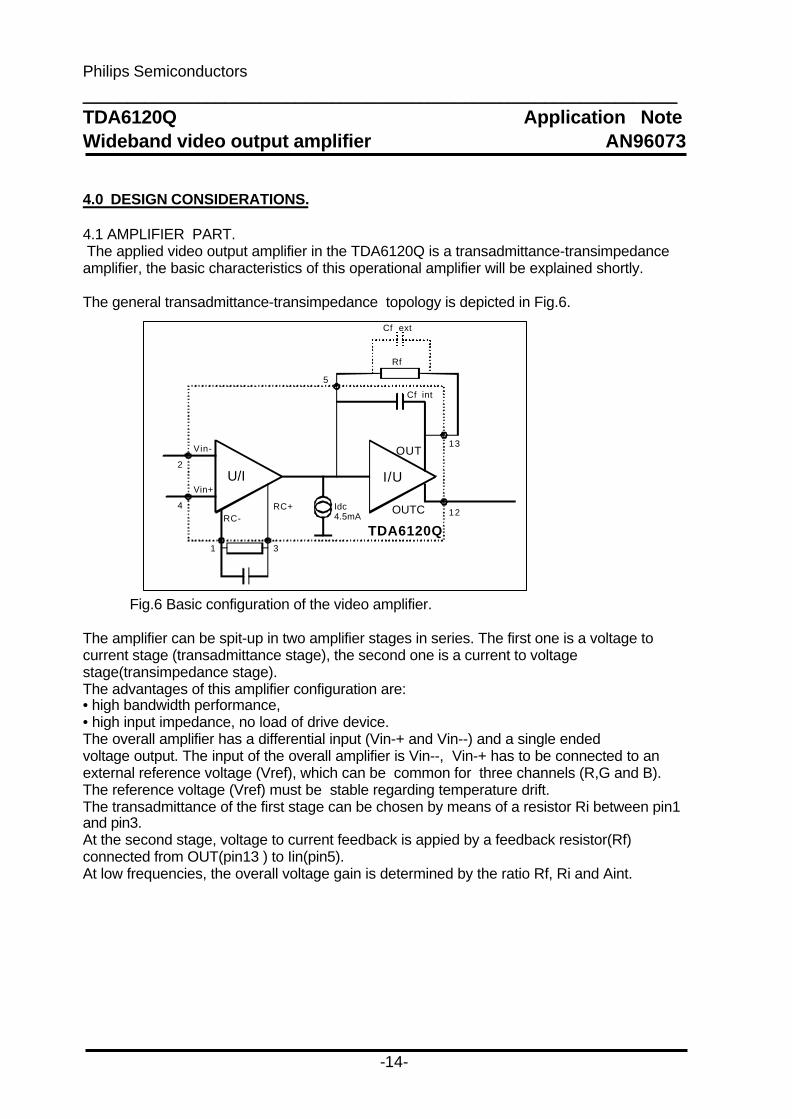
4.1 AMPLIFIER PART. The applied video output amplifier in the TDA6120Q is a transadmittance-transimpedanceamplifier, the basic characteristics of this operational amplifier will be explained shortly.
The general transadmittance-transimpedance topology is depicted in Fig.6.
Fig.6 Basic configuration of the video amplifier.
The amplifier can be spit-up in two amplifier stages in series. The first one is a voltage tocurrent stage (transadmittance stage), the second one is a current to voltagestage(transimpedance stage).The advantages of this amplifier configuration are:• high bandwidth performance,• high input impedance, no load of drive device.The overall amplifier has a differential input (Vin-+ and Vin--) and a single endedvoltage output. The input of the overall amplifier is Vin--, Vin-+ has to be connected to anexternal reference voltage (Vref), which can be common for three channels (R,G and B).The reference voltage (Vref) must be stable regarding temperature drift.The transadmittance of the first stage can be chosen by means of a resistor Ri between pin1and pin3.At the second stage, voltage to current feedback is appied by a feedback resistor(Rf)connected from OUT(pin13 ) to Iin(pin5).At low frequencies, the overall voltage gain is determined by the ratio Rf, Ri and Aint.
2
4
1 3
12
13
5
Vin-
Vin+
RC-RC+
Cf int
Idc4.5mA
Rf
Cf ext
U/I I/U
OUT
OUTC
TDA6120Q

Philips Semiconductors___________________________________________________________________TDA6120Q Application NoteWideband video output amplifier AN96073
-15-
4.2Voltage gain.
The overall voltage gain is defined by:
G = ∆Voutc = ∆Voutc = Aint . Rf/Ri. ∆ Vi (Vin+) - (Vin-)
WithVoutc = output cathode voltage (pin12)∆Vi = (Vin+) - (Vin-)Vin+ , Vin- = input voltages (pin2 and 4)Aint = internal gain of the amplifier, typical 1.87Rf = Feedback resistorRi = resistor between pin1 and 3. For most of the applications a voltage gain of 50-100 is sufficient to get 100Vp-p videooutput signals.
4.3 DC toDC transfer.
The DC voltage Voutc(dc) is determined externally by Ra, Rf ,Ri , and the level of Vin+ andVin- and internally by Aint and Idc.From equation:
Voutc(dc) = [Idc.Rf +2Vbe] + [ (Vin+ - Vin-) . Rf/Ri. Aint]with:Idc= internal current source, 4.5mA typ.
Hence, Vout(dc) >>2Vbe, we can approximate the equation:
Voutc(dc) = Rf ( Idc + ∆Vi/Ri .Aint ) = Rf (4.5 + ∆Vi /Ri . 1.87)
If Vin+ =Vin-, Voutc(dc) = Idc. Rf= 4.5 .Rf.
At Vin+=Vin- and Rf=22kΩ ===> Vout(dc) =100V.
Due to the differential input stage in combination with Rf and Ri, the TDA6120Q is veryflexible to fit with a lot of pre-amplifiers and CRTs.
From equation Vout(dc) = Rf ( Idc + ∆Vi/Ri .Aint ) the DC to DC transfer can be plotted atVin+=3V. This shown in Fig.1 of the product data on page 9.
4.4 Pole zero cancellation.The feedback resistor Rf and the parasitic capacitor Cf cause a pole in the transfer .For a value of Rf is >22kΩ this pole will cause a premature roll-off in the Bode plotand therefore a reduced overall small signal bandwidth.The value of Rf is a compromise between dynamic performance and dissipation.The bandwidth of the video amplifier can be improved by cancelling this pole by azero. This so called pole-zero cancellation can be done by placing a capacitor Ci

Philips Semiconductors___________________________________________________________________TDA6120Q Application NoteWideband video output amplifier AN96073
-16-
across the resistor Ri. The value of this capacitance is equal to:
Ci=Cf.Rf/Ri
When the Cf = Cfint + Cfext =0.7+0.1= 0.8pF and G =Rf/Ri=50, the capacitor Ci equals 40pF. To make extra speed-up, Ci can be chosen larger, dependent on the total amount (5% to10%) of overshoot required in the step-response. Speed-up can also partly compensate theroll-off in the input signal.
4.5 Stability.The stability of the TDA6120Q is in principle guaranteed by the design. In practice, the stability of the RGB board can be checked by :- measuring the frequency response of the system, the amplitude must be as flat as possible (within a few dB),- measuring the overshoot of a square wave signal.
4.6 Black current measurement output.
The TDA6120Q is provided with a black current data pin.The benefits to apply ABS are to compensate the differences in the gun characteristics duringwarming-up and ageing of the picture tube in order to have the correct colour balance inthe10µA region.The black current stabilisation loop is an automatic control loop which stabilises the blackcurrent of each channel sequentially and independently.To prevent that high video currents will flow in the black current input of the controlprocessor, the voltage on pin 7 of the TDA6120Q can be limited by an external zener diode.
4.7 Flash-over protection.
The TDA6120Q needs an external protection diode (BAV21) combined with a 50Ω resistor toprotect the video amplifier against CRT flash-over discharges.This diode clamps the cathode output voltage to Vdd+Vdiode. To limit the diode current, anexternal 220Ω carbon high-voltage resistor (Rfl) in series with the cathode output and a 2kVspark gap is recommended. The value of this carbon resistor is a compromise between videobandwidth and flash immunity.
More details about flash protection are given in chapter 7 -"Circuit application & applicationhints" and in the appendix of application note AN95064 ( see Reference).

Philips Semiconductors___________________________________________________________________TDA6120Q Application NoteWideband video output amplifier AN96073
-17-
5.0 EXTERNAL COMPONENTS CALCULATION.
The implementation of the TDA6120Q in an application requires the determination of externalcomponent values. These components are Rf, Ri,Ci and values of decoupling capacitors.In addition the dissipation of the IC and the feedback resistor Rf must be calculated in orderto obtain the kappa of the heatsink and the size of the feedback resistor respectively.
From equation : Voutc (dc) = Rf ( Idc + ∆Vi/Ri .Aint ) (5-1)
and: G= ∆Voutc. = Aint . Rf/Ri. (5-2) (Vin+) - (Vin-)
it can be seen that the value of the DC output voltage as well as the voltage gain dependsdirectly on the feedback resistor Rf. Hence Rf must be determined before calculating thevalue of Ri in order to obtain the correct gain and DC output voltage.
5.1 Feedback resistor Rf [R9,R12 and R15]
The value of Rf is a compromise between:- Dynamic performance: Rf must be as low as possible in order to obtain the optimumdynamic performance.- Minimum dissipation: Rf must be as high as possible in order to obtain the minimum staticdissipation , so a low cost resistor.A typical value of Rf is 22kΩ.Furthermore at this value of Rf holds Vout =100V , at Vin+=Vin-.In that case, the max. dissipation will be 1.8 Watt. (at Vdd=200V)
5.2 Input resistor Ri [R7,R10 and R13]
The input resistor can be calculated from the following formula:
Ri = Rf. Aint. (5-3) G
The board described in this report is designed to handle signals from TDA4780 andTDA4882 and here a voltage gain of 100 is sufficient to get 100Vp-p video output signals.For a gain of 100 ==> Ri= 430Ω.

Philips Semiconductors___________________________________________________________________TDA6120Q Application NoteWideband video output amplifier AN96073
-18-
5.3 Speed-up capacitor Ci [C5,C10 andC15]
The value of this capacitor can be calculated with : Ci = Cf . Rf. Ri (5-4)At Cf = Cfint + Cfext =0.7 +0.1 = 0.8 pF , ===>Ci = 39 pF.
As the layout of the chosen PCB is fixed, Ci can be determined for each channel.Depending on the layout of the PCB, Ci can be different for each channel.To avoid oscillations at very high frequencies, a stop resistor (R8,R11,R14=22Ω)has to beadded in series with this speed-up capacitor.At the evaluation board the speed-up capacitor consist of a fixed and a trimmer capacitor inparallel.Transient improvement can be obtained by increasing the speed-up capacitor by some pF,dependent on the amount of overshoot that is desired (5-10 %).To obtain a low inductance overall speed-up network, all components (except the trimmer)are in SMD technology.
5.4 Reference voltage Vin+.
Vin+ must be chosen in such a way that the typical blacklevel output voltage Vo(black) isclose to to the cut-off voltage (Vco) of the picture tube.The black level voltage Voutc(black) is determined by Rf and the level of Vin+ and Vin-(black). Vin- (black) is the typical value of the DC black level at the input and sothe typical value of the brightness control range of the video processor.Because Rf is fixed, Vin+ can be derived from the formula:
Voutc (dc) = Rf ( Idc + ∆Vi/Ri .Aint )
so that Vin+ = Voutc.Ri/Rf - (Idc.Ri )+ (Vin- . Aint.) = Voutc - Rf.Idc + Vin- (5-5) Aint G
If Vin-(black) = Vin+, Voutc(dc) = Rf.Idc
For a cut-off level of 160V ,Vi(black)= 3V , Rf=22kΩ and Ri= 430Ω ==> Vin+ = 3.6V
5.5 Vdd & Vcc decoupling (C2,C3,C7,C8,C12,C13)
The low voltage supply pin ( Vcc) as well as the high voltage suppy pin must be decoupledwith a capacitor of 100nF with short leads and with good HF characteristics, placed as closeas possible between the supply pins and GND.To obtain optimal decoupling and low inductance leads, SMD components are applied forthis on the evaluation board.

Philips Semiconductors___________________________________________________________________TDA6120Q Application NoteWideband video output amplifier AN96073
-19-
5.6 Decoupling regarding flash [C21,C22,C23 and C16)]
To protect the video amplifiers against picture tube flash-over discharges the high supplyvoltage (Vdd) must be decoupled by a capacitor >20nF/250V (e.g. a film capacitor of100nF/250V with short leads and with good HF characteristics), placed as close as possibleto the Vdd supply line and GND of each TDA6120Q and definitely within 5mm. Thiscapacitor limits voltage excursions of Vdd during the first part (Trise=10 nsec) of a lowresistance flash.
∆ U = I(flash). T. = Vspark (max.) . T rise = 4 kV . 10 nsec = 1.3 V C Rfl Ch.f 1k5 20 nF
at Ch.f. = 100nF , ∆ U= 0.25V.
with: V(spark(max.) = maximum ignition voltage of the sparkgap,Trise = rise time of the cathode voltage to exceed the Vspark(max.),Rfl= flash resistor,Ch.f= high frequency decoupling capacitor.
The high supply voltage (Vdd) must also be decoupled with a capacitor >10uF/250V on theCRT board . This capacitor limits the voltage excursion during a high resistance flash. Forthe calculation of this voltage excursion it is supposed that there is no ignition of the sparkgap and that the picture tube discharges completely through the external flash diode. In thatcase the maximal voltage excursion will be:
∆U = Ctube . Veht = 2n7 . 28 kV = 7.5 V Cl.f 10µF
with: Ctube = capacitance of the picture tube,Veht = voltage of extra high tension,Cl.f = low frequency decoupling capacitor.
This capacitor is common for the three channels, the position is less critical but must belocated on the CRT board.
5.7 Flash diodes [D1,D2 andD3]An external high voltage reverse biased diode has to be connected between the OUTC of theTDA6120Q and the Vdd line, with short leads.The diode must be able to surge high flash currents. A BAV21 diode has been chosen forthis. The position on the board and lead length in conjuction with the flash capacitors (C21,22,23) is very important.
For more detailed information about these capacitors and flash diode see chapter 7.6 flash-over protection .

Philips Semiconductors___________________________________________________________________TDA6120Q Application NoteWideband video output amplifier AN96073
-20-
5.8 Additional components on the main CRT board.
5.8.1 Voltage /Current feedback.
When using TDA4882 or TDA4780 voltage or current feedback (ABS) can be applied .Therefor the main CRT board is provided with the X2 connector,which can deliver therequired voltages (FbR, FbG ,FbB) and current (Ioutm).
5.8.2 Current feedback (Switch S4).
A zener diode D4 of 12V is applied to prevent that high video currents will flow intothe black current input of the pre-amplifier. In this case the voltage is limited to 12V. Becausethe supply voltage of the TDA4780 is 8V, a 6V8 zener is added on the TD4780 add-on board.When dark current feedback is applied, switch S4 must open.If not using the ABS function, switch S4 can be closed , in that case the Iom outputs areshort circuit to ground with capacitor C4 via the switch and there will be no cross-talk from theIom outputs to the inputs. See for more details chapter7.7 .
5.8.3 Voltage feedback (switch S1,S2,S3).
In combination with the TDA4882 add-on board , the resistors R25,R27 and R29 are used forvoltage feedback.
5.8.4 Stop resistors regarding h.f stability.
To avoid possible high frequency oscillations in the input leads, stop resistors of 100Ω areapplied in the Vin+ and Vin- leads.

Philips Semiconductors___________________________________________________________________TDA6120Q Application NoteWideband video output amplifier AN96073
-21-
6.0 DISSIPATION & HEATSINK CALCULATION.
6.1 Static and dynamic dissipation.The components dissipating power are the TDA6120Q and the feedback resistors.The dissipation of the TDA6120Q consists mainly of the static contribution of the quiescentcurrent and the dynamic dissipation caused by high frequency drive (proportional tofrequency)
The static dissipation of the TDA6106Q is due to the voltage supply current and the loadcurrents in the feedback resistors and CRT.The static dissipation equals:
Pstat = Vcc.Icc + Vdd. Idd - [Voutc.(Voutc/Rf - Ioutc)] + Vcc.Icc (6-1)
Ioutc = DC value of the cathode current.Voutc = DC value of the cathode voltage.With Vdd=200V, Vcc=12V, Voutc=100V , Iccmax =39 mA and Iddmax=12 mA thestatic dissipation equals : Pstat= 2.9 W.
The dynamic dissipation equals:Pdyn = Vdd . ( Cl + Cint ) . f . Vo p-p . b. (6-2)
Cl = load capacitance (Ctube, Csocket, Cspakgap, Cdiode, Cpar)Cint = internal load capacitance (7 pF)f = input frequencyVo p-p = output voltage (peak to peak)b = non blanking duty cycle.
Regarding the dynamic dissipation, we have to distinguish two application areas.• High resolution TV applications• Monitor applications.
6.1.1 High resolution TV.The input bandwidth is defined by the control processor.When using the TDA4780, the bandwidth is 22MHz and the output signal of 100Vp-pat the cathode of the CRT.
With Vo p-p=100V, f=22MHz (sine wave), Cl=10 pF, Cint=7 pF and b=0.8, thedynamic dissipation Pdyn. equals: 6.6 W.
The total dissipation Ptot=Pstat+Pdyn under given conditions is 9.2 W.

Philips Semiconductors___________________________________________________________________TDA6120Q Application NoteWideband video output amplifier AN96073
-22-
6.1.2 Monitor application.To obtain well focused pictures, the max. output voltage at the cathode of the CRT will be75Vp-p.For the bandwidth 30MHz has been chosen, this means an input step responce of about10nS, which is a rather practical value.
With Voutc p-p=75V, f=30MHz (sine wave), Cl=10 pF, Cint=7 pF and b=0.8, the dynamicdissipation Pdyn. equals: 6.4 W.
The total dissipation Ptot=Pstat+Pdyn under given conditions is 9.3 W.
6.2 HEATSINK CALCULATION
Thermal parameters of the TDA6120Q:Rth,j-mb = 3 K/W (typ).The Rth,mb-heatsink = 0.5 K/W depends on mounting method of the heatsink.Tj,max= 150oCTamb,tv= 65oC
If the max. operating temperature in a TV set is about 65 oC, with a power dissipation of Wand a thermal resistance Rth,j-mb of 3K/W, a heatsink has to be applied with a thermalresistance of:
Rth,heatsink = (Tj-Tamb). - Rth,j-mb - Rth,(mb-heatsink) [K/W] (6-3) Ptot
Rth,heatsink = (Ths-Tamb). (6-4) Ptot
For High resolution TV, Rth,heatsink≤ 5.74 K/W
For monitor applications, Rth,heatsink≤ 5.64 K/W
On the main RGB board described in this report, a standard heatsink is used.This heatsink has an Rth,hs of 5.6 K/WWith this heatsink , under normal maximum dissipation as calculated (9.3W) the heatsinktemperature will rise to 117 oC and the junction temperature to 145 oC which is just withinthe limits of the IC.This means that the use of better PC board material for the main CRT board is desired.
6.3 Absolute worst case conditions.
At absolute worst case conditions ,125Vp-p @ 30MHz , Tamb,tv =65oC andRth,heatsinh=5.6K/W, the heatsink temperature will rise to 140 oC and the junctiontemperature to 169 oC which is outside the limits of the TDA6120Q.

Philips Semiconductors___________________________________________________________________TDA6120Q Application NoteWideband video output amplifier AN96073
-23-
6.4 A more practical approach regarding dissipation
In the previous part, the dissipation has been calculated for the TDA6120Q.However, this is a rather theoretical approach and in practice it differs from this, in particularthe dynamic dissipation. This will be explained now.In a TV set the worst case of dissipation occurs with :• a noise signal (from the tuner) in TV mode,• a multi-burst pattern (1-30MHz) in AV mode.Furthermore, it is not realistic that there will be a continuous picture containing a full screen of30 MHz sine wave signals .Measurements in a TV set show a lower dynamic dissipation in TV and AV mode comparedwith the calculated values given in the previous part.Therefore, a correction factor (Cth ) can be applied for the dynamic dissipation.However, when a smaller heatsink is used as calculated in the previous part, the TDA6120Qmust be protected by a thermal protection circuit .The basic circuit diagram for this is shown in Fig.7.
Dissipation @Rth,hs=5.6K/w
conditions Pstat[W]
Pdyn[W]
Ptotal[W]
Theatsink[oC]
Tjunction[ oC]
absolute max. 2.9 10.6 13.5 140 169normal max. 2.9 6.4 9.3 117 145practical Cth=0.6 2.9 3.8 6.7 102 122
Table 1 Overview of dissipation
Fig.7 Thermal protection for the TDA6120Q
R4
C1
R3
D1
D2
D3
T1
R1
R2
T2
Vdd
Pull downcontrast
Red
Blue GreenVideoamp.
TDA6120Q

Philips Semiconductors___________________________________________________________________TDA6120Q Application NoteWideband video output amplifier AN96073
-24-
7.0 CIRCUIT APPLICATION & APPLICATION HINTS
In this chapter information is given concerning the application of the TDA6120Q as videooutput stage. The circuit diagram of a complete video output stage for use in a TV-set isgiven in Fig. 18 on page 38. The circuit application is optimised for handling the outputsignals from the video processor TDA4780 and TDA4882 in order to drive a flat square black-line CRT, with an EHT of 28kV and a cut-off voltage of 160V.The signal gain is 40 dB and the output swing is 100Vp-p.To obtain max. performance, TDA6120Q as well as the pre-amplifier (e.g. TDA4882 orTDA4780) should be mounted on the CRT panel.
7.1 DESIGN-IN SEQUENCE of the TDA6120Q .
To simplify the design-in of the TD6120Q, the design is summarized below:• determine the cut-off voltage of the CRT (Tube Handbook),• determine the required video drive for the CRT and the available drive from the colour processor and calculate the signal gain .• determine the value of the feedback resistor Rf, see section 5.1• calculate Ri with equation 5-3 given in section 5.2• calculate Ci with equation 5-4 given in section 5.3• determine the nominal value of black level of the colour processor,• calculate reference voltage with equation 5-5, given in section 5.4• calculate the power dissipation with equation 6-1 and 6-2 , given in section 6.0• calculate the thermal resistance of the required heatsink with equation 6-3, given in section 6.2
7.2 Printed Circuit Board.The PCB shown in this report on page 30 is meant for evaluation purposes.The CRT base socket is JEDEC B10-277. The connectors X1(R,G,B,Vin+,GND) and X2(FbB,FbR, FbG.Iom) ) are pin alligned with the connectors of the add-on boards.The main CRT board of the TDA6120 is constructed with single-sided copper.
To get the optimal signal performance, special attention has to be payed on the followingpoints of the PCB layout.- keep h.f. current loops as short as possible,- seperate large and small signal current paths,- minimize parasitic capacitance, keep hf-signal tracks as narrow as possible,- use star point grounding, make ground and supply tracks as wide as possible.
- Concerning supply decoupling & Ri/Ci network. Because of the very high bandwidth, use low inductance components (SMD) for h.f supply decoupling and the Ci/Ri network.

Philips Semiconductors___________________________________________________________________TDA6120Q Application NoteWideband video output amplifier AN96073
-25-
- Concerning flash-over protection :The most important thing is that h.f. flash decoupling capacitor (C21,C22,C23=100nF)has to be placed as close as possible between the Vdd line and GND of eachTDA6120 and an external high voltage reverse biased diode has to be connectedbetween the OUTC of the TDA6120Q and the Vdd line, with very short leads.The total current path (diode & capacitor) must be as short as possible, in order toavoid high L.di/dt voltages. See also the position of flash diodes and capacitorsgiven at the PCB layout in Fig.19 .A detailed example of a correct and incorrect layout regarding flash protection isgiven in Fig.8a and Fig.9.The electrolytic capacitor (C16 =10 µF) has to be mounted on the CRT panel, the position onthe board is not critical .
Fig.8a Correct Fig.9 Not correct.

Philips Semiconductors___________________________________________________________________TDA6120Q Application NoteWideband video output amplifier AN96073
-26-
7.3 Crosstalk.
The different parasitic links which induce cross-talk are shown in Fig.10 (2 ampl.)The parasitic coupling is caused by parasitic capacitances.
Fig. 10 Parasitic Capacitors.
The cross-talk can be caused by:- parasitic coupling between the inputs.(Cpi),- parasitic coupling between the outputs (Cpo),- parasitic coupling between an output and an input of another channel (Cpoi).
The third type of parasitic coupling is dominant since it involves the coupling of relatively highlevel output signals with relatively low level input signals.The parasitic coupling between inputs and outputs must be minimized to achieve anacceptable crosstalk of better than 20dB at 10 MHz.This can be done by crossing only the input wires and separating the input and output leads.Large signal components and wires must be laid out as far as possible from small signalwires.High frequency radiation from the feedback resistors must not induce a voltage signal at theinput of another channel. This can be achieved by:• put enough space between the feedback resistors,• mount these resistors in the same direction and strictly align one next to the other,• using ground shields to isolate the input wires.
Vin
Vin
Vout
Vout
Rfl
Rfl
CpiCpoi
Cpo

Philips Semiconductors___________________________________________________________________TDA6120Q Application NoteWideband video output amplifier AN96073
-27-
7.4 Switch-off behaviour.
When a TV receiver is being switched-off , several voltages become low.The cathode output voltage of the TDA6120Q is dependent on the input condition of Vin+ &Vin- , Vcc and Vdd.The switch-off behaviour of the TDA6120Q is defined and controllable.
There are two types of switch-off behaviour:
7.41 Voutc follows Vdd, after switch off, -Type A-Voutc=f(t) is shown in fig.11This kind of switch-off is most generaly used.The fall time of Voutc is determined by the fall time of Vdd and can be adapted by the valueof the decoupling capacitor on Vdd. The minimum value (10µF) is limited by flash overbehaviour.
7.42 Voutc is switched to zero, after switch off while Vdd = high, -Type B-.Voutc=f(t) is shown in fig.12In this case the Ceht of the CRT will be discharged directly after switch off. This can be asafety requirement of the setmaker for service/repair.
Fig.11 Fig.12Upper: Vdd= f(t) ,50V/div, 250mS/div. Upper: Vdd= f(t) ,50V/div, 250mS/div.Lower: Voutc= f(t) ,50V/div, 250mS/div. Lower: Voutc= f(t) ,50V/div, 250mS/div.Vdd decoupling C16=10µF Vdd decoupling C16=10µFThe 1-> and 2-> markers show the ground level.1-> for the lower trace and 2-> for the upper trace.
Philips Semiconductors___________________________________________________________________TDA6120Q Application NoteWideband video output amplifier AN96073
-28-
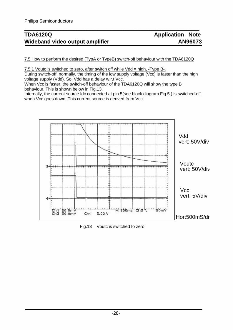
7.5 How to perform the desired (TypA or TypeB) switch-off behaviour with the TDA6120Q
7.5.1 Voutc is switched to zero, after switch off while Vdd = high, -Type B-.During switch-off, normally, the timing of the low supply voltage (Vcc) is faster than the highvoltage supply (Vdd). So, Vdd has a delay w.r.t Vcc.When Vcc is faster, the switch-off behaviour of the TDA6120Q will show the type Bbehaviour. This is shown below in Fig.13.Internally, the current source Idc connected at pin 5(see block diagram Fig.5 ) is switched-offwhen Vcc goes down. This current source is derived from Vcc.
Vddvert: 50V/div
Voutcvert: 50V/div
Vccvert: 5V/div
Hor:500mS/div
Fig.13 Voutc is switched to zero

Philips Semiconductors___________________________________________________________________TDA6120Q Application NoteWideband video output amplifier AN96073
-29-
7.5.2 Voutc follows Vdd ,after switch off, -Type A-Type A switch-off behaviour can be obtained if Vcc goes down after Vdd and Vin+>Vin-.This is shown in Fig.14 .As can be seen from the curves, the timing of Vdd and Vcc will define the kind of swich-offbehaviour.At the moment Vcc goes down to zero, the switch-off behaviour of type B will be there.So, at typeA switch-off behaviour, the timing of Vdd and Vcc is very important.
Vddvert: 50V/div
Voutcvert: 50V/div
Vccvert: 5V/div
Hor:500mS/div
Fig.14 Voutc follows Vdd ,after switch off,

Philips Semiconductors___________________________________________________________________TDA6120Q Application NoteWideband video output amplifier AN96073
-30-
7.6 Flash-over protection.
A picture tube has generally several high voltage discharges in its life time.During the discharge (flash), an overvoltage can occur on the cathodes. This overvoltage candamage the RGB video amplifier, since it is directly connected to the CRT.The TDA6120Q needs an external flash protection diode combined with a 50Ω resistor toprotect the video amplifier against CRT flash-over discharges. The diode clamps the cathodeoutput voltage to Vdd+Vdiode. To limit the diode current, an external 220Ω carbon high-voltage resistor (Rfl) in series with the cathode output and a 2kV spark gap is recommended.The value of this carbon resistor is a compromise between video bandwidth and flashimmunity.
Essential for flash-over protection is the connection between aquadag and mainPCB(deflection/supply board). In our concept the aquadag is connected to the sparkgap onthe CRT board and from here a connection to the main board. See fig.15.Furthermore a separate earth wire must be connected from the ground of the CRT board tothe line/supply main board.
The max. allowed peak supply voltage during a flash may not exceed 220V.As the max. operating voltage is 210V, the delta voltage caused by a flash may not exceed10 volts.To prevent that the supply peak voltage never exceeds 220V, the value and position ofdecoupling capacitors is very important.
Fig.15 Grounding of aquadag & RGB board.
The following remarks are very important w.r.t. flash protection.
C h.f.
E.H.T.28kV
Vdd
MAIN PCB
Sparkgap
AquadagTo ground ofline/supply
8
10
CRT
C l.f.
12
BAV21
220Ω
TDA 6120Q
50Ω

Philips Semiconductors___________________________________________________________________TDA6120Q Application NoteWideband video output amplifier AN96073
-31-
•To protect the TDA6120Q against fast voltage peaks during a low-ohmic flash Vdd must bedecoupled with a capacitor >20nF/250V with good h.f properties and placed as close aspossible between Vdd and GND, but definitely within 5mm.This is necessary, otherwise a voltage peak can occur due to the inductance of the long wiresbetween the TDA6120Q pins and the capacitor (V= L di/dt) and this voltage peak candamage the IC.
• For the discharge of the CRT during a high-resistance flash an electrolitic capacitor of≤10µF/250V is necessary, mounted on the CRT board.
• For the TDA6120Q, external flash diodes have to be applied at each output The leads of the diodes must be kept as short as possible.
• Ignition level of the sparkgap must be typical 2kV and worst case <4kV.
• Flash resistors must be high voltage carbon composite types (e.g. Allen Bradley)
• To have a short primary flash loop, earth connections of aquadag and sparkgaps are veryimportant.Connect the aquadag ground via a short wire ( and low inductance) to the earth of thesparkgap, and from here with a wire to the ground of the line transformer on the main PCB.The inductance can be made small, e.q. by keeping it close to the surface of the picture tube.The ground of the TDA6120Q must be connected via a separate wire to the ground of the linetransformer on the main board. The wire diagram is shown in Fig. 15 .
• Grid G1 connection. In a lot of applications, grid G1 can be directly connected to aquadag ground. In that case the flash resistor can be omitted in the G1 connection to create a permanentlow impedance path for the flash current and thus better protect the cathodes , with the videooutput amplifiers.The direct aquadag grounding of G1 can't be applied when measuring the EHT info, this willbe discussed in the next part.
7.6.1 Flash -protection for alternative aquadag grounding.
The basic application described in this report is designed for an application in which thebeam current of the EHT is measured by using a "beam current " capacitor Cbc in the lineoutput stage.In that case, the lower side of the EHT transformer is not connected to ground (for instancethe TDA837X & supply demonstration kit of PS-SLE).Therefore, special attention has to be given to flash-over behaviour.The simplified circuit diagram is given in Fig.16.

Philips Semiconductors___________________________________________________________________TDA6120Q Application NoteWideband video output amplifier AN96073
-32-
Fig.16 Alternative aqua grounding.
In case of a high resistance flash the current is low and the sparkgap does not ignite. Duringthat flash the aquadag capacitor Ctube is discharged and the charge will transfer via Rfland the internal flash diode to the capacitors Cl.f. // Ch.f. and Cbc.The available charge of Ctube will be distributed across these capacitors.When Ctube= 4 nF, Cbc=22nF and Cl.f.=10 µF the capacitor Cbc is charged at a level ofseveral kilo Volts with a negative polarity w.r.t supply ground.At a level of 2kV the sparkgap ignites and the voltage over Cbc will be present on the outputof the TDA6120Q, resulting in a damaged IC.To prevent this, a suppression/limiter device (zenerdiode + a series diode) or VDR has to beplaced from the aquadag wire (lower side of the sparkgap) on the CRT board to supplyground. This is shown in Fig.16 (limiter device).The suppression device must be a medium power type to handle the flash currents.
More detailed information about flash protection is given in the Appendix of the applicationnote AN95064( see reference) .
C h.f.C l.f.
Vdd
SparkgapLimiter-device
+Vf
E.H.T.
Lineoutputtransformer
Cbc
Grounding ofaquadag &RGB-board
Groundline/supply
8
10
Beamcurrentinfo.
220Ω
BAV21
E.H.T.28kV
Aquadag
CRTCtube
TDA 6120Q12
50Ω

Philips Semiconductors___________________________________________________________________TDA6120Q Application NoteWideband video output amplifier AN96073
-33-
7.7 Black current stabilisation.
The most simple application of the TDA6120Q in an automatic black current set-up inconjunction with the video processor TDA4780 is shown in Fig. 17 .The black current stabilisation loop is an automatic control loop which stabilises the blackcurrent of each channel sequentially and independently every field.The loop is active for a four line period , immediately after the end of the field blanking.During field scan (outside the 4L black current measuring time) , the normal video currentflows in the ABS feedback path.To prevent that high video currents will flow in the TDA4780 black current input, the voltageon pin 7 of the TDA6120Q is limited by an internal built in zener diode of 20V.The TDA4780 has I2C bus adjustments for the white point, the gain and colour balance inthe 10µA region, therefore no adjustments are required for gain and black setting at theTDA6120Q application.The black current input of the TDA4780 is a low impedance current driven input with leakcurrent compensation.
Fig.17 Basic ABS application with the TDA6120Q and TDA4780.
E.H.T.28kV
Aquadag
TDA6120QCRT
RGB
Black
TDA4780
currentinput
outputs10
212
7
8
+Vdd
beam current
RGB
G RB
Sparkgap
BAV21
220Ω
100nF10µF
50Ω

Philips Semiconductors___________________________________________________________________TDA6120Q Application NoteWideband video output amplifier AN96073
-34-
8.0 PERFORMANCE EVALUATION.
The evaluation board has been designed to obtain the best results.To evaluate the h.f performance , the best way is to measure outside the TV set by driVin-gthe amplifier by an h.f. generator or network analyzer.The "passive' add-on board ( see appendix) can been used as interface between thegenerator and the TDA6120 main board.The flash behaviour has to be examined in a TV set. In this situation the TDA6120Q as wellas the application are tested.
Measurement conditions for h.f. :
The schematic diagram of the h.f measurement set-up is shown in Fig 20 on page 41.• High voltage supply Vdd=200V• Biasing: Voutc(DC)=100V• AC Gain: 40 dB• Ioutm(pin7) is decoupled with a capacitor of 100nF to ground.• Loading: see curves• All measurement results include a flash resistor of 220Ω and Ct=5pF Ct is the cathode capacitance of the CRT. The total load capacitance Cltotal, including Csocket, Csparkgap, Cdiode and the parasitic capacitances of the PCB , will be about 10pF. The value of the flash resistor is a compromise between flash-over behaviour and bandwidth.
Measurement Results:
8.1 Bandwidth.
The measurement set-up is given in Fig.20 on page 41.The curves in Fig.23 and 24, on page 43, show the frequency response with 60Vp-p and100Vp-p output voltages at optimal Ci.Rfl=220Ω and Ctube 5pF (total load capacitance about 10pF.Bandwidth at 60Vp-p, amounts to 41.5 MHz. (-3dB)Bandwidth at 100Vp-p, amounts to 40 MHz. (-3dB)In Fig.25 the small- signal bandwidth is shown at different values of Ci.
8.2 Multi-burst performance.
In Fig.26 the multi-burst performance of the TDA6120Q is shown at Vout = 60Vp-p.The multi- burst frequencies are 2,5,10,15,20 and 25MHz.

Philips Semiconductors___________________________________________________________________TDA6120Q Application NoteWideband video output amplifier AN96073
-35-
8.3 Cross-talk.
The measurement set-up is given in Fig.21 on page 41.A sine wave input signal is injected in one channel and the output signal of one of the otherchannels is measured.
Cross-talk = 20 log Voutc ( drive channel) . [dB]Voutc (one of the other channels)
The curves given in Fig.27, 28 and 29 on page 45 and 46 show the cross-talk of thisapplication board at which Voutc= 60Vp-p .The worst value at 20 MHz is 26dB.The cross-talk is not the same for the six different combinations of the three channels.In table 2 on page 46 the cross-talk is given of the six combinations at f=20 MHz.
8.4 Rise and fall time.
The curves Fig.31 and 32 on page 47 and 48 respectively show the rise and fall time at100Vp-p output signal of the red channel.Typ. value Tf= 12.1 nSec. at 100Vp-p, with Rfl=220Ω, Cl=10pF and Ci=39pFTyp. value Tr= 10.8 nSec. at 100Vp-p, with Rfl=220Ω, Cl=10pF and Ci=39pFThe fall/rise time of the input signal is 10nSec.In Fig.30 the pulse response and overshoot is shown at the same conditions.Table on page 48 shows the fall and rise time at 100Vpp and different values of Ci.Table on page 48 shows the fall and rise time at 125Vpp and different values of Ci.
8.5 Flash test.
Fig. 22 on page 42 shows the test set-up applied for flash-over tests by Philips.With this test, the TDA6120Q as well as the application are tested.
Test conditions:TV set with 33 inch soft flash picture tube, Veht=28 kV.So the total available charge will be Q= Ctube.Veht = 3.5nF. 28kV= 100 µC.Number of flashes: 50
8.5.1 High-resistance flash.
During high resistance flashes , the sparkgap does not ignite and the total charge transfersvia the flash resistor Rm, Rfl and the flash diode into the electrolytic decoupling capacitor ofVdd.Where Rm is the simulation of the arc resistance in the CRT between g4 and the cathode.In practice , the minimum value of Rm at which the sparkgap does not ignite is :
Rm= Rfl(Veht - V(spark) = 220Ω. (28-4)kV= 1k3 V(spark) 4kΩ
Philips Semiconductors___________________________________________________________________TDA6120Q Application NoteWideband video output amplifier AN96073
-36-
with:Vign of the sparkgap is worst case (4kV), Veht=28kV and Rfl=220Ω.
Under given conditions, the peak current amounts to Veht / (Rm+ Rfl)=28kV / (1k3+220Ω)= 18.6 A.At the high resistance flash-test, switch S1 is closed (Rfl=0 Ω), which means that thesparkgap can not ignite.To test at various values of flash currents, the value of Rm has to be adapted.
8.5.2 Low -resistance flash.
During low-resistance flashes , S1 is open, the sparkgap ignites and only a little charge (during the first part of the flash) tranfers via the flash resistor Rfl and the flash diode into theh.f decoupling capacitor of Vdd.Very fast peak voltages can occur on the Vdd pin of the TDA6120Q , the h.f. capacitor has toprevent the device for these peak voltages.At a low-resistance flash , the resistor Rm (equivalent of the arc of the CRT) is typical 400Ωand worst case 200Ω for a soft flash picture tube.
Philips Semiconductors___________________________________________________________________TDA6120Q Application NoteWideband video output amplifier AN96073
-37-
9.0 ACKNOWLEDGMENT.
This project was done with help of students of Technical College Ede during the practiceperiod.The students involved are:G.J. v. Holland PCB layout, schematics and demo board assemblyL. v. Zanten Measurements, schematics and demo board assembly
10. REFERENCES.
1) DATA SHEET TDA6120Q.2) DATA SHEET TDA47803) DATA SHEET TDA48824) Soft-flash colour tubes, PHILIPS COMPONENTS Technical publication 2535) Flashover in picture tubes and methods of protection. - By A. Ciuciura.- The Radio and Electronic Engineer, Vol.37, No3, March 1969.6) Application and product description of the TDA6106Q video output amplifier. -AN 95064- By: E.H Schutte.7) 22 Mhz Video amplifier for large jumbo picture tubes . -AN95008- By: J.J Hekker.8) Video amplifier for HR monitor with TDA4882 and TDA6120. -AN9507- By: J.J Hekker.9) Video amplifiers for VGA/XGA monitors. -ETV93001- By: H.J.S. Aben.
11 APPENDIX
1) Imperfections of the TDA6120Q.
2) "Passive" interface add-on board.
3) Application TDA4882 add-on board.
4) Application TDA4780 add-on board.

Philips Semiconductors___________________________________________________________________TDA6120Q Application NoteWideband video output amplifier AN96073
-38-
Fig. 18 Application diagram of the TDA6120Q.
TUB
E
EHT
g1g2
g3
A66E
AK.
.X43
RED
GRE
EN
BLUE
VIN+
VIN
-VC
CG
ND
VDO
OU
TC
RC-
RC+
IINO
UTM
n.c.
n.c.
OU
TTD
A612
0Q
24
68
1012
13
57
911
13
VIN+
VIN
-VC
CG
ND
VDO
OU
TC
RC-
RC+
IINO
UTM
n.c.
n.c.
OU
TTD
A612
0Q
24
68
1012
13
57
911
13
VIN+
VIN
-VC
CG
ND
VDO
OU
TC
RC-
RC+
IINO
UTM
n.c.
n.c.
OU
TTD
A612
0Q
24
68
1012
13
57
911
13
Gre
enIC
1
IC 2
IC 3
Red
Blu
e
kG kR kB1186
910
57
1
12V
Vip
FbB
FbR
FbG
Iom
200V
Aqua
Vff+
12V
Vff-
GND
GN
D
GN
D
GN
D
*=>O
ptio
nal
***
#=>N
ot p
resen
t on
6120
v31
PCB
L1
22uH
L2
22uH
D1
Bav
21
D2
Bav
21
D3
Bav
21
RV
1
35V
S1 S2
X1
12345678
X2
1 2 3 4
X3
1 2 3 4 5 6
X5A
QU
AV
G2
X4
R7
431E
R10
431E
R13
431E
R19
10E
R20
1E2
R21
10E
R2
21K
5R
231K
5
C1
10n
C2
100n
C4
18p
C5
33p
C6
10n
C7
100n
C10
33p
C11
10n
C12
100n
C14
18p
C15
33p
C9
18p
C19
1n
S4
C3
100n
C21 10
0n
C8
100n
C22
100n
C1
310
0n
C23
100n
S3
R16
220E
R17
220E
R18
220E
R24
100
R9
22K
R8
22E
R1
100
R2
100
R26 10
0
R1
222
K
R11
22E
R3
100
R4
100
R28
100
R15
22K
R14
22E
R5
100
R6
100
R29
150K
R2
7
150K
R2
515
0K
C20
100n
D4
12V
C1
8
2n7
+C16
10u
+C17
47u
200
200
200
12
12 12 12
12
200
Philips Semiconductors___________________________________________________________________TDA6120Q Application NoteWideband video output amplifier AN96073
-39-
PART LIST.
Position no. VALUE RATING TYPEIntegrated Circuit(s) TDA6120Q
CapacitorsC1,C6,C11 10nF SMDC2,C7,C12 100nF SMDC3,C8,C13 100nF SMDC5,C10,C15 33pF SMDC4,C9,C14 18pF Adjustable capacitorC16 10µF 250V ElectrolyticC17 47µF 16V ElectrolyticC18 2n7 500V Ceramic plateC19 1nF 2000V MKTC20 100nF 64V MKTC21,C22,C23 100nF 250V MKT
Resistors.R1,R2,R3,R4,R5,R6 100Ω SFR16TR7,R10,R13 430Ω SMDR8,R11,R14 22Ω SMDR9,R12,R15 22kΩ 2W- PR02R16, R17,R18 220Ω High V. Allen Bradley -1/2 WR19,R21 10Ω NFR25R20 1.2Ω NFR25R22,R23 1k5 High V. Allen Bradley -1/2 WR24,R26,R28 100Ω NFR25R25,R27,R29 150kΩ SFR16TR30,R31,R32 50Ω SFR16
DiodesD1,D2,D3 BAV21D4 12V BZX79C12
VDRRV1(Varistor) 35V
Special partsX1 8-pole connectorX2 4-pole connectorX3 6-pole connectorPicture tube socket, with integrated sparkgaps EDEC B10-277

Philips Semiconductors___________________________________________________________________TDA6120Q Application NoteWideband video output amplifier AN96073
-40-
Scale: 1:1
Fig.19 TDA6120Q Evaluation board layout & components view.

Philips Semiconductors___________________________________________________________________TDA6120Q Application NoteWideband video output amplifier AN96073
-41-
Fig.20 Bandwidth measurement set-up
Fig. 21 Crosstalk measurement set-up
Rfl
Rfl
Rfl
R
G
B220Ω
100nF
HP 3577NETWORKANALYSER
S R
AAttenuator -20dB
ActiveProbe-40dB
Ci
1µF
1µF
1µF
50Ω
ActiveProbe-40dB
PCB TDA6120Q
5p6
Rfl
Rfl
Rfl
R
G
B
220Ω
220Ω
220Ω
HP 3577
NETWORKANALYSER
S
R
A
PCB TDA6120Q
1µF
1µF
1µF
50Ω
Active Probe -40dB
Active Probe -40dB
5,6pF
5,6pF
100nF
100nF
Ci
Ci

Philips Semiconductors___________________________________________________________________TDA6120Q Application NoteWideband video output amplifier AN96073
-42-
Fig.22 Flash-over test set-up.
Rfl = 220Ω
The value of Rm depends on type of test (200Ω -10kΩ) and is built with resistors in series.Type: Allen Bradley - high voltage.Rm is the simulation of the arc resistance in the picture tube between the EHT and thecathode.
Flashmill
C h.f.
E.H.T.28kV
Vdd
MAIN PCB
Sparkgap
AquadagTo ground ofline/supply
8
10
CRT
S1
Dig. scope
Currentprobe
Rm
C l.f.
12
BAV21
220ΩTDA 6120Q

Philips Semiconductors___________________________________________________________________TDA6120Q Application NoteWideband video output amplifier AN96073
-43-
vert. : 3dB/divGain[dB]
Measuremntafter Rfl
Rfl=220ΩCload=10pFCi=39pF
Vdd=200VVoutc-dc=100V
Voutc-ac=60V
-------> f [Hz]
Fig.23 Small signal bandwidth of the TDA6120Q
vert.:3dB/di.Gain [dB
Measurementafter Rfl
Rfl=220ΩCload=10pF
Ci=33pF
Vdd=200VVoutc-dc=100VVoutcac=100V
-------->f [Hz]
Fig.24 Large signal bandwidth of the TDA6120Q.

Philips Semiconductors___________________________________________________________________TDA6120Q Application NoteWideband video output amplifier AN96073
-44-
vert. : 3dB/div.Gain[dB]
Measurementafter Rfl
Rfl=220ΩCload=10pF
Vdd=200VVoutc-c=100VVoutc-ac=60V
Ci= 33,39 and47pF
------->f [Hz]
Fig.25 Small signal bandwidth as function of Ci .
Voutc
Vi
Fig.26 Multi-burst performance of the TDA6120Q.Voutc-dc=100V, Voutc-ac=100Vpp, Ci=optimal=33pFf= 2,5,10,15,20 and 25MHz

Philips Semiconductors___________________________________________________________________TDA6120Q Application NoteWideband video output amplifier AN96073
-45-
vert. : 10 dB/div.Cross-talk [dB]
Measurementafter Rfl
Rfl=220ΩCload=10pF
Vdd=200VVoutc-c=100VVoutc-ac=60V
------->f [Hz
Fig.27 Crosstalk behaviour of the TDA6120Q - source= R, crosstalk=B
vert. : 10 dB/div.Cross-talk [dB]
Measurementafter Rf
Rfl=220ΩCload=10pF
Vdd=200VVoutc-c=100VVoutc-ac=60V
-------> f[Hz]
Fig.28 Crosstalk behaviour of the TDA6120Q - source= G, crosstalk=B

Philips Semiconductors___________________________________________________________________TDA6120Q Application NoteWideband video output amplifier AN96073
-46-
vert. : 10 dB/div.Cross-talk [dB]
Measurementafter Rfl
Rfl=220ΩCload=10pF
Vdd=200VVoutc-c=100VVoutc-ac=60V
--------->f [Hz]
Fig.29 Crosstalk behaviour of the TDA6120Q - source= G, crosstalk=R
Crosstalk Blue Crosstalk Red Crosstalk GreenSignal Blue X 26dB 27dBSignal Red 30dB X 28dBSignal Green 35dB 30dB X
Table 2 Crosstalk at a frequency of 20 MHz.

Philips Semiconductors___________________________________________________________________TDA6120Q Application NoteWideband video output amplifier AN96073
-47-
Fig.30 Pulse response of the TDA6120Q at Voutc= 100Vp-pMeasured with Rflash = 220Ω , Cl=10pF, Ci=39pFHor: 200nS/div Vert: upper Vi=0.4V/div , lower Voutc=40V/div.
Fig.31 Rise time of the TDA6120Q at Voutc= 100Vp-pMeasured with Rflash = 220Ω , Cl=10pF, Ci=39pFHor: 25 nS/div Vert: 15V/div

Philips Semiconductors___________________________________________________________________TDA6120Q Application NoteWideband video output amplifier AN96073
-48-
Fig.32 Fall time of the TDA6120Q at Voutc= 100Vp-pMeasured with Rflash = 220Ω , Cl=10pF, Ci=39pF
Hor: 12.5nS/div Vert: 15V/div
Voutc=100Vpp Trise [nSec] Tfall [nSec] Ci=33pF 12.9 12.3 Ci=39pF 10.8 12.1 Ci=47pF 9.8 12.2
Table 3. Rise/Fall time=f(Ci) of the TDA6120Q at Voutc= 100Vp-pMeasured with Rflash = 220Ω , Cl=10pF
Voutc=125Vpp Trise [nSec] Tfall [nSec] Ci=33pF 13.4 14.3 Ci=39pF 11.8 14.6 Ci=47pF 12.6 14.9
Table 4. Rise/Fall time=f(Ci) of the TDA6120Q at Voutc= 125Vp-pMeasured with Rflash = 220Ω , Cl=10pF
Philips Semiconductors___________________________________________________________________TDA6120Q Application NoteWideband video output amplifier AN96073
-49-
APPENDIX 1IMPERFECTIONS OF TDA6120Q.
• Flash performance. To obtain sufficient flash performance, the TDA6120Q/N1 needs a small series resistor of 50Ω in the output (pin12). In that case, it is allowed to apply a maximum operating voltage of 210V. For that resistor a low cost 0.5 watt resistor (SFR16) can be applied.
Note. These resistors are not present on the evaluation PCB.
• Current measurement output. The measurement output IOUTM is fully functional up to a junction temperature of 125oC i.s.o 150oC. Furthermore the offset current is too high. The nominal value is 20µA with a minimum value of -40µA and a maximum value of +120µA (see DATA sheet). For three amplifiers in parallel this becomes a high value. This offset current is constant, so if the dynamic range of of the Automatic Black- current Stabilisation (ABS) is large enough, this offset current will be seen as a large leakage current , so if the offset current can be compensated, the ABS loop will work satisfactory. Furthermore , the lower side of the operating window is rather high, 4V>Voutm>20V, and does not fit optimal with the TDA4780.
• ESD The maximum allowable ESD voltage for the N1 is 2000V HBM and 300V MM, except for pin 5. For pin5 holds: HBM, 1250V and for MM 300V.
• Distortion. A sinusoidal signal shows distorsion at frequencies above 8MHz.

Philips Semiconductors___________________________________________________________________TDA6120Q Application NoteWideband video output amplifier AN96073
-50-
APPENDIX 2
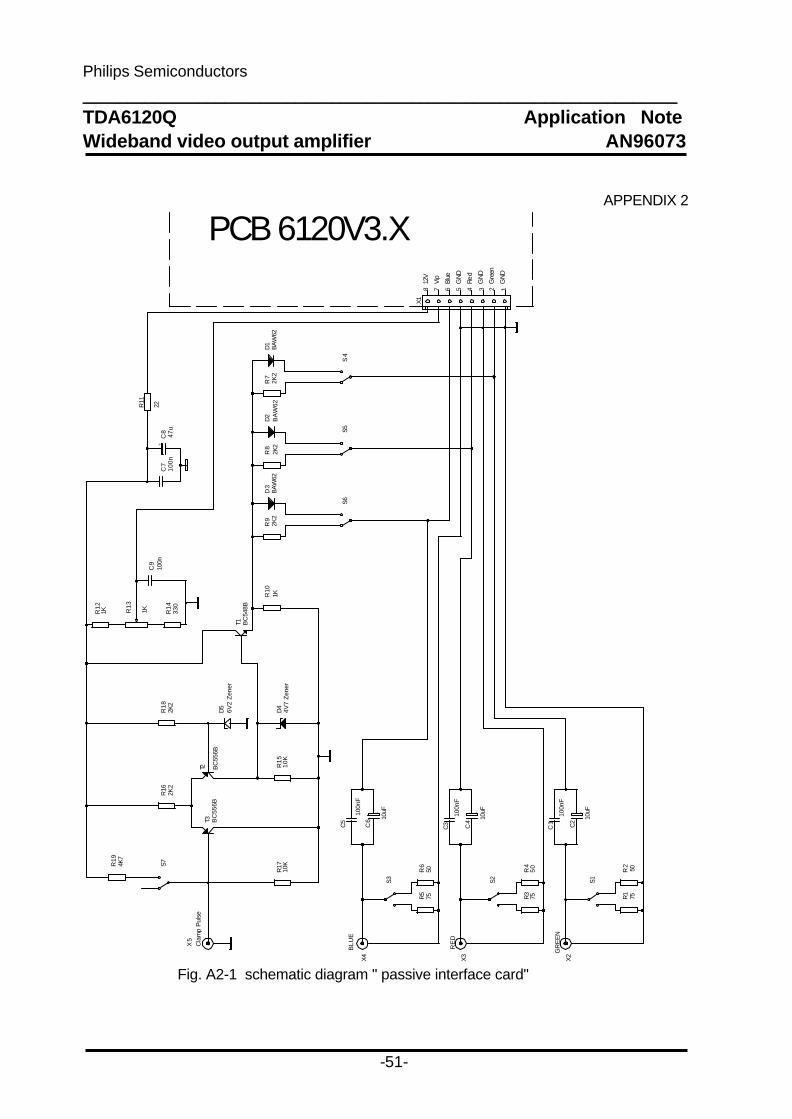
• INTERFACE - add-on board •
This board can be applied to drive the TDA6120 directly from a testpattern generator or awaveform generator.In that case the real TDA6120Q performance can be tested.The board fits with the CRT main board and can be used as plug-in board.This add-on board is constructed with double-sided copper.The schematic diagram is given in Fig.A2-1The layout and components view is shown in Fig.A2-2
Two modes are available:• wave signal mode• testpattern mode.
Wave signal mode.
Switch settings:- Set S1,S2,S3 in 50Ω position,- Set S7 in on position (voltage divider R17,R17 active)- Set S4,S5,S6 in 2k2 position.
In this mode the input impedance is 50Ω.The input signals from connector X2,X3 and X4 will be set to a dc level of about 4V, whichare availabe at pin 2,4,6 of connector X1.By means of the potentiometer R13 the dc level of Vin+ (Vref) can be adjusted and isavailable at pin 7 of connector X1.
Testpattern mode.
Switch settings:- Set S1,S2,S3 in 75Ω in position,- Set S7 in off position,- Set S4,S5,S6 in diode position,- Apply a positve keying pulse of >6.5V to connector X5.
In this mode the input impedance is 75Ω.During the active keying pulse the input signals from connector X2,X3 and X4 will beclamped to a dc level of about 4V,(during the back porch of the line sync. pulse).The clamped RGB signals are availabe at pin 2,4,6 of connector X1.By means of the potentiometer R13 the dc level of Vin+ (Vref) can be adjusted and isavailable at pin 7 of connector X1.
Philips Semiconductors___________________________________________________________________TDA6120Q Application NoteWideband video output amplifier AN96073
-51-
APPENDIX 2
Fig. A2-1 schematic diagram " passive interface card"
12V
Blue
GND
Red
GND
Gre
en
GND
Vip
PCB 6120V3.X
BLU
E
X4
RE
D
X3
GR
EE
N
X2
X1
12345678
C3
100n
F
+
C4
10uF
C7
100n
+C
847
u
C9
100n
C1
100n
F
+
C2
10uF
C5
100n
F
+
C6 10
uF
R1
75
X5
Cla
mp
Pul
se
D3
BA
W62
D2
BA
W62
D1
BA
W62
D5
6V2
Zen
er
R2
50R4
50
R3
75R5
75R
650
R7
2K2
R8
2K2
R9
2K2
R10
1K
R11
22
R12
1K R14
330
R15
10K
R16
2K2
R17
10K
R18
2K2
R19
4K7
S7
S6S5
S4
D4
4V7
Zen
er
S3 S2 S1
R13
1K
T3 BC
556B
T2 BC
556B
T1 BC
548B

Philips Semiconductors___________________________________________________________________TDA6120Q Application NoteWideband video output amplifier AN96073
-52-
APPENDIX 2
scale: 1: 1
Fig.A2-2 •Interface card - layout & components view •
Philips Semiconductors___________________________________________________________________TDA6120Q Application NoteWideband video output amplifier AN96073
-53-
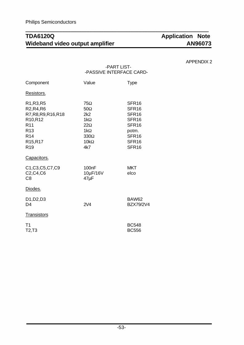
APPENDIX 2 -PART LIST-
-PASSIVE INTERFACE CARD-
Component Value Type
Resistors.
R1,R3,R5 75Ω SFR16R2,R4,R6 50Ω SFR16R7,R8,R9,R16,R18 2k2 SFR16R10,R12 1kΩ SFR16R11 22Ω SFR16R13 1kΩ potm.R14 330Ω SFR16R15,R17 10kΩ SFR16R19 4k7 SFR16
Capacitors.
C1,C3,C5,C7,C9 100nF MKTC2,C4,C6 10µF/16V elcoC8 47µF
Diodes.
D1,D2,D3 BAW62D4 2V4 BZX79/2V4
Transistors
T1 BC548T2,T3 BC556

Philips Semiconductors___________________________________________________________________TDA6120Q Application NoteWideband video output amplifier AN96073
-54-
APPENDIX 3
•TDA4882 ADD-ON BOARD •CONTENTS.
• INTRODUCTION
• ADDITIONAL APPLICATION INFORMATION.
• CIRCUIT APPLCATION DIAGRAM
• PCB LAYOUT & COMPONENTS VIEW
• PARTLIST
• PERFORMANCE OF THE TDA4882 & TDA6120Q COMBINATION
INTRODUCTION.This board equipped with the TDA4882 can be applied as pre-amplifier to drive theTDA6120Q.The TDA 4882 is a RGB pre-amplifier for colour monitor systems with super VGAperformance. A complete product description is given in the DATA sheet.By using this combination , the concept is suitable for monitor applications.The combination has a total bandwidth of 30-60 MHz , depending on the cathode outputswing requirement and is suitable for VGA, SVGA and XGA applications.The schematic appication diagram is given in Fig.A3-2The PCB layout is shown in Fig.A3-3This add-on board fits with the TDA6120Q CRT main board and can be used as plug-inboard , the connectors are pin aligned.During the application evaluation period of this project, the TDA4885 be came available.All funtions are the same as the TDA4882. Redarding the interface between the TDA4885and TDA6120Q the output levels of the TDA4885 fits much better.Note.For more details of the TDA4882 , see DATA sheet TDA4882 and application noteETV93001 (see reference).
ADDITIONAL APPLICATION INFORMATION.
Layout of the Printed Circuit Board.The layout of the TDA4882 is critical, special attention should be given to the groundingtracks around the IC.In general it can be said that the layout must be made such, that current loops do not overlapin order to separate large and small signal currents.The grounding tracks and loops must be kept as small as possible .Because of the very high bandwidth, this printed circuit board is constructed with doublesided copper.

Philips Semiconductors___________________________________________________________________TDA6120Q Application NoteWideband video output amplifier AN96073
-55-
APPENDIX 3
The interface between pre-amplifier TDA4882 and output amplifier TDA6120Q.
The voltage output of the TDA4882 does not fit with the operating range of the differentialinput of the TDA6120Q regarding DC level.This problem is solved by a DC level shift from GND for the TDA4882.In that case , the output voltages of the TDA4882 are shifted with about 3.4 V.The interface is shown in Fig.A3-1.
Rf
12V
12
Ci
TDA4882
Vs
Gnd
TDA6120Q
C1 8V2
47Ω
300Ω 1k
7k5
22Ω 430Ω
2
1
3
4
5
13
8
7
4
14,17,20
13,16,19
30Ω
Fig.A3-1. Combination TDA4882 and TDA6120Q
The TDA4882 video pre amplifier input circuit. (connector X1,X2,X3)
All the video input signals are terminated with 75Ω to ground.The video signal is AC coupled to the input of the TDA4882.The inputs of the TDA4882 are terminated to ground with a 10MΩ resistor to prevent blacklevel drift when no clamp pulse is present.The input voltage (black to white value) is typical 0.7V and max.1V.
Available output voltage ( connector X5)
The nominal signal output ( black to white value) at pin 2,4,6 of connector X5 amounts to0.8V at nominal contrast and nominal gain setting.The gain of the red channel is fixed, the blue and green gain can be controlled by the pot.meters R4 and R35.

Philips Semiconductors___________________________________________________________________TDA6120Q Application NoteWideband video output amplifier AN96073
-56-
APPENDIX 3
The timings signals at pin 9 and pin10 of the TDA4882. (connector X4)
Pin 10.Two timing signals:- the horizontal clamping pulse- the vertical blanking pulse.
pin10 (threshold) Min. Typ. Max. UnitVertical Blanking- Blanking-No input clamping
1.2 1.4 1.6 V
Clamping- Input clamping- No blanking
2.6 3.0 3.5 V
Pin 9.Two timing signals:- the blanking puse- the switch-off signal
pin10 (threshold) Min. Typ. Max. UnitBlanking- Blanking- Output clampingclamping
1.2 1.4 1.6 V
Switch off- Min. black level-No output clamping
5.8 6.5 6.8 V
Alternatives for blanking & clamping pulses.
Using the TDA4851.The combination of TDA4851(Advanced Monitor Deflection Processor) and the TDA4882 isthe most optimal solution to generate/use the timing needed for clamping and blanking.
Cut-off voltage stabilization. ( Connector X6 and switches S1,S2 and S3 )
For cut-off stabilization the video signal at the output of the TDA6120Q is divided by anadjustable voltage divider to the feedback inputs (pin18,15,12) of the TDA4882.During the horizontal blanking time this signal is compared with an internal DC voltage. Theblack level voltage Voutc(black) of the TDA6120Q can be adjusted by means ofpotentiometers R20,R23 and R26, present on the TDA4882 add-on board.

Philips Semiconductors___________________________________________________________________TDA6120Q Application NoteWideband video output amplifier AN96073
-57-
Fig.A3-2 Application diagram of theTDA4882 add-0n board
Vip
Vert
Blan
k
Hor
Blan
k
12V
Blue
Red
Gre
en
Blue
Red
Gre
en
Gre
en
Red
Blue
GND
GND
GND
Brig
htnes
s
Gain
B
Contr
ast
Gain
G
Cut-
off B
Cut-o
ff R
Cut-
off G
PCB 6120VER3X
* =>
Opt
ion
al
&Bu
rst k
ey
= R
ef l
evel
= 3
.5V
at V
cc =
12V
Not
e:
1 2 3 4 5 6 7 8 9 1011121314151617181920
U1 TD
A48
82
X2
X4
123
C2
22n
R2
75
R3
10M
X3 X1
L1
22u
C1
22nC
3
22n
C4
100n
+C
510
0uD
18V
2
X6
1234
X5
12345678
R5
75
R6
10M
R8
75
R9
10M
R10
1KR
1110
K
R12
1KR
1310
K
R18
6K8
R19
15K
R21
6K8
R22
15K
R24
6K8
R25
15K
R29
300
R30
30
R31
300
R32
30
R33
300
R34
30
C7
100n
C8
100n
C9
100n
+C
10
100u
R28
7K5
R27
1KC
11
100n
C6
100n
*R
144
7R
17
10
R16
10
R15
10
R1
10K
R4
10K
R7
10K
R20
10K
R23
10K
R26
10K
R35 10
K
12V
12V
12V
12V
12V
12V
12V
12V
12V
12V
12V
12V

Philips Semiconductors___________________________________________________________________TDA6120Q Application NoteWideband video output amplifier AN96073
-58-
APPENDIX 3
Fig.A3-3 PCB layout & Components view

Philips Semiconductors___________________________________________________________________TDA6120Q Application NoteWideband video output amplifier AN96073
-59-
APPENDIX 3
-PART LIST- - TDA4882 ADD-ON BOARD-
Component Value Type
IC TDA4882
Resistors.
R1,R4,R7 10kΩ potm.R2,R5,R8 75Ω SFR16R3,R6,R9,R11 10MΩ SFR16R10,R12,R27 1kΩ SFR16R11,R13 10kΩ SFR16R14 47Ω SFR16R15,R16,R17 10Ω SFR16R18 6k8 SFR16R19,R22,R25 15kΩ SFR16R20,R23,R26,R35 10kΩ potm.R28 7k5 SFR16R29,R31,R33 30Ω SFR16R30,R32,R34 300Ω SFR16
Capacitors.
C1,C2,C3 22n MKTC4,C6,C7,C8,C9,C11100nF MKTC5,C10 100µF/16 Elco
Diodes.
D1 8V2 BZX79/8V2

Philips Semiconductors___________________________________________________________________TDA6120Q Application NoteWideband video output amplifier AN96073
-60-
APPENDIX 3PERFORMANCE OF THE TDA4882 & TDA6120Q COMBINATION
The pulse reponse performance was tested of the TDA4882 & TDA6120 combination.The pulse response and rise& fall times are shown in Fig. A3-4,A3-5 and A3-6.
Measurement conditions :• High voltage supply Vdd=200V• Low voltage supply Vcc=12V• Biasing: Voutc(DC)=100V• AC Gain TDA6120 : 40 dB• Voltage feedback: active (switch S1,S2,S3).• Ioutm(pin7) is decoupled with a capacitor of 100nF to ground (switch S4).• Rise & fall time of the square wave input signal is 10nS.• Loading: see curves• All measurement results include a flash resistor of 220Ω and Ct=5pF Ct is the cathode capacitance of the CRT. The total load capacitance Cltotal, including Csocket, Csparkgap, Cdiode and the parasitic capacitances of the PCB , will be about 10pF.
Fig.A3-4 Pulse response of the TDA4882 & TDA6120Q combination. Voutc =100Vp-p. Measured with Rflash = 220Ω , Cl=10pF, Ci=39pF
Hor: 50nS/div Vert: upper Vi=0.5V/div , lower Voutc=20V/div

Philips Semiconductors___________________________________________________________________TDA6120Q Application NoteWideband video output amplifier AN96073
-61-
Fig.A3-5 Rise time of the TDA4882&TDA6120Q combination .Voutc= 100Vp-p . Meaured with Rflash = 220Ω , Cl=10pF, Ci=39pF Hor: 25 nS/div Vert: 20V/div
Fig.A3-6 Fall time of the TDA4882 & TDA6120Q combination . Voutc= 100Vp-p. Measured with Rflash = 220Ω , Cl=10pF, Ci=39pF
Hor: 5nS/div Vert: 20V/div

Philips Semiconductors___________________________________________________________________TDA6120Q Application NoteWideband video output amplifier AN96073
-62-
APPENDIX 4
•TDA4780 ADD-ON BOARD •
CONTENTS.
• INTRODUCTION
• ADDITIONAL APPLICATION INFORMATION.
• CIRCUIT APPLCATION DIAGRAM
• PCB LAYOUT & COMPONENTS VIEW
• PARTLIST
• PERFORMANCE OF THE TDA4882 & TDA6120Q COMBINATION
INTRODUCTION.
This board equipped with the TDA4780 can be applied as pre-amplifier to drive theTDA6120Q.The TDA 4780 is a RGB processor with automatic cut-off control for TV systems with HighResolution performance. A complete product description is given in the DATA sheet.By using this combination, the concept is suitable for High Resolution TV applications.The combination has a total bandwidth of 22MHz .With this concept there are no alignments any more, because of the automatic black currentstabilisation and because the white point adjustment can be done in the TDA4780 via I2Cbus.The principle of automatic black current stabilisation (ABS) was given in chapter 7.7 .The schematic application diagram of the TDA4780 is given in Fig.A4-2The PCB layout is shown in Fig.A4-3This add-on board fits with the TDA6120Q CRT main board and can be used as plug-inboard , the connectors are pin aligned.
ADDITIONAL APPLICATION INFORMATION.
Layout of the Printed Circuit Board.
In general it can be said that the layout must be made such, that current loops do not overlapin order to separate large and small signal currents.The layout of the TDA4882 is critical, special attention should be given to the groundingtracks around the IC.The grounding tracks and loops must be kept as small as possible .Because of the high bandwidth, this printed circuit board is constructed with double sidedcopper.

Philips Semiconductors___________________________________________________________________TDA6120Q Application NoteWideband video output amplifier AN96073
-63-
The interface between TDA4780 & TDA6120Q. The interface between the TDA4780 and TDA6120Q is shown below in Fig. A4-1The DC & AC output levels of the TDA4780 fit with the input levels of the TDA6120Q.
Rf
12
Ci TDA6120Q
1k
22Ω 430Ω
41
3
7
5
13
814
24(22,20)2
1k
TDA4780
8V
82K 6V8 100pF
2V4 100nF
Fig.A4-1 Combining the TDA4780 and TDA6120Q.
The TDA4780 video processor input circuit. (connector X5,X2,X7)By using these inputs , the TDA4780 has to be set in R1,G1,B1 mode via I2C bus.All the video (R,G,B) input connectors are terminated with 75Ω to ground .The video signals are AC coupled to the inputs of the TDA4780.The R,G,B input voltage (black to white value) is typical 0.7V.
Sandcastle input (connector X4)
The TDA4780 must have a two- or three-level ( selected through I2C) sandcastle signal foroperation.
I2C bus signals (connector X3)
The TDA4780 needs I2C data.
Note.For more details about the TDA4870, see DATA sheet TDA4870

Philips Semiconductors___________________________________________________________________TDA6120Q Application NoteWideband video output amplifier AN96073
-64-
APPENDIX 4
Fig. A4-2 Application diagram of the TDA4780 add-on board
12V
Vip
Blue
Red
Gre
en
Iom
Blu
e
Re
d
Gre
en
SC
LSD
A
GN
D
GN
D
GN
D
GN
D5V
SC
BC
L
PCB6120V3.X
GN
DY-(
R-Y
)-(
B-Y
) B2
G2
R2
1 2 3 4 5 6 7 8 91
0
11
12
13
14
28 27 26 25 24 23 22 21 20 19 18 17 16 15
TD
A47
80
U1 *
**
*
*
*=>
Opt
iona
l
X1
1234
C2
100n
C3
100n
C8
330n
C10
220n
C11
220n
C12
220n
C17
100n
X2
12345678
X3
1
2
3
4
C18
100n
C19
100n
D2
6.8V
D3
6.8V
C6 10
0n
C14
100n
C15
100n
C13
100n
D1
2V4
C20 10
0n
C21 100n
C22
100n
C23
100n
C24
100n
C25
470n
C26
100p
X4
123
X5 X6
X7
X8
1
2
3
4
5
6
7
8
C16
100n
C27
10n
R5
100
R4
100
R6
75R
775
R8
75R
975
R10
1K
R3
82K
R1
22
R2
1K
R11
75R
127
5R
1375
R14
75
R15 1K
U3
78L0
5
VIN
GND
VO
UT
U2
78L0
8
VIN
GND
VO
UT
R18 10
0R
17 100
R16 10
0
R21
R20
R19
+C
71u
+C
110
0u
+C
422
u
+C
91u
+C
5
12V
12V
12V

Philips Semiconductors___________________________________________________________________TDA6120Q Application NoteWideband video output amplifier AN96073
-65-
APPENDIX 4
Fig.A4-3 PCB layout & Components view of the TDA4780 add-on board

Philips Semiconductors___________________________________________________________________TDA6120Q Application NoteWideband video output amplifier AN96073
-66-
APPENDIX 4
-PART LIST- - TDA4780 ADD-ON BOARD-
Component Value Type
IC TDA4780
Resistors.
R1 22Ω SFR16R2,R10,R15 1kΩ SFR16R3 82kΩ SFR16R4,R5 100Ω SFR16R6,R7,R8,R9,R10, 75Ω SFR16R11,R12,R13,R14 75Ω SFR16R16,R17,R18 100Ω SFR16
Capacitors.
C1 100µF/16V ElcoC2,C3,C6 100nF MKTC4 22µF/16V ElcoC7,C9 1µF/16V ElcoC8 330nF MKTC10,C11,C12 220nF MKTC13,C14,C15,C16,C17 100nF MKTC18,C19,C20,C21,C22 100nF MKT
Diodes.D1 2V2 BZX79/2V4D2,D3 6V8 BZX79/6V8

Philips Semiconductors___________________________________________________________________TDA6120Q Application NoteWideband video output amplifier AN96073
-67-
APPENDIX 4
PERFORMANCE OF THE TDA4780 & TDA6120Q COMBINATION
The pulse reponse performance is measured of the TDA4882 & TDA6120 combination.The results are shown inFig.A4-4, A4-5 and A4-6.Furthermore the multi-burst performance is measured , this is shown in Fig.A4-7, A4-8, A4-9and A4-10.
Measurement conditions :
• High voltage supply Vdd=200V• Low voltage supply Vcc=12V• Biasing: Voutc(DC)=100V• AC Gain TDA6120 : 40 dB• Voltage feedback: not active (switch S1,S2,S3).• Ioutm(pin7) : active (Switch S4• Loading: see curves• All measurement results include a flash resistor of 220Ω and Ct=5pF Ct is the cathode capacitance of the CRT. The total load capacitance Cltotal, including Csocket, Csparkgap, Cdiode and the parasitic capacitances of the PCB , will be about 10pF.
Fig.A4-4 Pulse response of the TDA4780 & TDA6120Q combinationVoutc= 100Vp-p. Measured with Rflash = 220Ω , Cl=10pF, Ci=39pFHor: 50nS/div Vert: upper Vi=1V/div , lower Voutc=20V/div.

Philips Semiconductors___________________________________________________________________TDA6120Q Application NoteWideband video output amplifier AN96073
-68-
APPENDIX 4
Fig.A4-5 Rise time of the TDA4780 & TDA6120Q combination .Voutc= 100Vp-p. Measured with Rflash = 220Ω , Cl=10pF, Ci=39pF
Hor: 12.5 nS/div Vert: 20V/div
Fig.A4-6 Fall time of the TDA4780 & TDA6120Q combination.
Voutc= 100Vp-p. Measured with Rflash = 220Ω , Cl=10pF, Ci=39pFHor: 12.5nS/div Vert: 20V/div.

Philips Semiconductors___________________________________________________________________TDA6120Q Application NoteWideband video output amplifier AN96073
-69-
Small signal Multi - burst performance APPENDIX 4
Voutc20V/div
Vi0.5V/div
Fig.A4-7 Multi-burst performance of the TDA4780 &TDA6120Q. Voutc-dc=100V, Voutc-ac=60Vpp, Ci=optimal=33pF f= 1,2,3,4,5 and 6 MHz
Voutc20V/div
Vi0.5V/div
Fig.A4-8 Multi-burst performance of theTDA4780&TDA6120Q. Voutc-dc=100V, Voutc-ac=60Vpp, Ci=optimal=33pF f= 10,12,14,16,18 and 20MHz

Philips Semiconductors___________________________________________________________________TDA6120Q Application NoteWideband video output amplifier AN96073
-70-
Large signal Multi- burst performance APPENDIX 4
Voutc20V/div
Vi0.5V/div
Fig.A4-9 Multi-burst performance of the TDA4780 & TDA6120Q. Voutc-dc=100V, Voutc-ac=100Vpp, Ci=optimal=33pF f= 1,2,3,4,5 and 6 MHz
Voutc20V/div
Vi0.5V/div
Fig.A4-10 Multi-burst performance of the TDA4780 &TDA6120Q. Voutc-dc=100V, Voutc-ac=100Vpp, Ci=optimal=33pF f= 10,12,14,16,18 and 20MHz

Philips Semiconductors___________________________________________________________________TDA6120Q Application NoteWideband video output amplifier AN96073
-71-