APPLICATION NOTE: Minimizing Input Filter Requirements In ...venable.biz/tech-pubs/Minimizing Input...
19
1 ©2017 Venable Instruments. For more information, go to www.venable.biz Keywords Venable, frequency response analyzer, MIL-STD-461, input filter design, open loop gain, voltage feedback loop, AC-DC, transfer function, feedback control loop, maximize attenuation output, impedance, control loop APPLICATION NOTE: Minimizing Input Filter Requirements In Military Power Supply Designs Abstract: Military power supplies frequently require conducted susceptibility testing per MIL- STD-461. Essentially, this test consists of treating the power supply as a filter, and measuring the attenuation of input signals as a function of frequency. This paper describes the relationship between open-loop gain of the voltage feedback loop and input filter characteristics. Design techniques to meet conducted emission and conducted susceptibility requirements are presented. Design guidelines are presented and topologies and operating modes that aid in meeting the requirements are suggested. Introduction Input filters are a necessary but unpopular component of every military power supply. They are large, heavy, and expensive. They solve some problems, but create others. Yet because of specifications like MIL-STD-461, "Electromagnetic Emission and Susceptibility Requirements for the Control of Electromagnetic Interference," they are absolutely necessary. The choice is not whether or not to use an input filter, but how to minimize the size, weight, cost, and adverse impact on performance. Functions Of An Input Filter Desirable Characteristics Input filters serve two primary purposes. From a system designer's standpoint, the input filter prevents electromagnetic interference or "noise" which is generated in all switching power sources from reaching the power bus and affecting other equipment. In this case, the purpose of the filter is to attenuate the AC portion of the power supply input current so that only a small portion of it reaches the power bus. The filter functions as a reverse current filter. From a user's standpoint, the input filter prevents high frequency AC voltage on the power bus from passing through to the outputs of the power supply and on to the using equipment. The feedback control loop allows the power supply to reject low frequency AC voltage on its input, but above the loop crossover frequency there is little the loop can do to reject noise. In this case, the purpose of the input filter is to attenuate the AC voltage superimposed on the DC power bus so that only a small portion of it reaches the power supply input terminals. The filter functions as a forward voltage filter, attenuating input noise. Fortunately, passive filters have the characteristic that forward voltage attenuation is identical to reverse current attenuation. This allows one input filter to satisfy the needs of both system designers and end users.
Transcript of APPLICATION NOTE: Minimizing Input Filter Requirements In ...venable.biz/tech-pubs/Minimizing Input...

1
©2017 Venable Instruments. For more information, go to www.venable.biz
Keywords Venable, frequency response analyzer, MIL-STD-461, input filter design, open loop gain, voltage feedback loop, AC-DC, transfer function, feedback control loop, maximize attenuation output, impedance, control loop
APPLICATION NOTE:
Minimizing Input Filter Requirements In Military Power Supply Designs
Abstract:
Military power supplies frequently require conducted susceptibility testing per MIL-STD-461. Essentially, this test consists of treating the power supply as a filter, and measuring the attenuation of input signals as a function of frequency. This paper describes the relationship between open-loop gain of the voltage feedback loop and input filter characteristics. Design techniques to meet conducted emission and conducted susceptibility requirements are presented. Design guidelines are presented and topologies and operating modes that aid in meeting the requirements are suggested.
Introduction
Input filters are a necessary but unpopular component of every military power supply. They are large, heavy, and expensive. They solve some problems, but create others. Yet because of specifications like MIL-STD-461, "Electromagnetic Emission and Susceptibility Requirements for the Control of Electromagnetic Interference," they are absolutely necessary. The choice is not whether or not to use an input filter, but how to minimize the size, weight, cost, and adverse impact on performance.
Functions Of An Input Filter
Desirable Characteristics Input filters serve two primary purposes. From a system designer's standpoint, the input filter prevents
electromagnetic interference or "noise" which is generated in all switching power sources from
reaching the power bus and affecting other equipment. In this case, the purpose of the filter is to
attenuate the AC portion of the power supply input current so that only a small portion of it reaches
the power bus. The filter functions as a reverse current filter.
From a user's standpoint, the input filter prevents high frequency AC voltage on the power bus from
passing through to the outputs of the power supply and on to the using equipment. The feedback
control loop allows the power supply to reject low frequency AC voltage on its input, but above the
loop crossover frequency there is little the loop can do to reject noise. In this case, the purpose of the
input filter is to attenuate the AC voltage superimposed on the DC power bus so that only a small
portion of it reaches the power supply input terminals. The filter functions as a forward voltage filter,
attenuating input noise. Fortunately, passive filters have the characteristic that forward voltage
attenuation is identical to reverse current attenuation. This allows one input filter to satisfy the needs
of both system designers and end users.

2
©2017 Venable Instruments. For more information, go to www.venable.biz
Undesirable Side Effects
The penalty, which must be paid in size, weight, and cost from implementing an input filter, has already
been mentioned. Performance penalties are in addition.
If there is insufficient damping--and this is more the rule than the exception--the transfer function
(gain) of the filter peaks near its resonant frequency. This peak causes amplification of input noise at
the resonant frequency, so that noise voltage applied at the input of the filter is actually larger in
amplitude when it reaches the input terminals of the power supply. If this condition happens at a
frequency which is above or not far below the bandwidth of the feedback control loop, the power
supply will not be able to reject the disturbance and the specification for allowable AC voltage on the
outputs of the power supply may be exceeded.
In addition to amplification, poorly damped filters have a significant impact on the transfer function of
the feedback control loop. There is a dip in both gain and phase at the resonant frequency of the filter.
In moderate cases, this results in power supply output transient response that rings at the input filter
resonance, even though the true control loop crossover frequency may have ample gain and phase
margins. In more extreme cases, the input filter can cause the control loop to oscillate. The output
impedance of the input filter peaks at resonance, and it has been shown that if the peak of the input
filter output impedance exceeds the input impedance of the power supply at that frequency, the loop
will oscillate.
Typical Filter Characteristics
A block diagram of a typical system with the simplest possible L-C filter is shown in Figure 1. The power source is typically 28 VDC from an aircraft, spacecraft, or other vehicle. There is AC noise superimposed on the DC source voltage and the L-C filter is supposed to attenuate this noise. The output of the L-C section drives a DC/DC converter, which in turn supplies regulated DC voltages to using equipment.
Figure 1. Simple L-C Input Filter

3
©2017 Venable Instruments. For more information, go to www.venable.biz
A plot of the transfer function or "gain" of the L-C filter is shown in Figure 2. Below the L-C resonant frequency, voltage passes through the filter without significant attenuation. Above the L-C resonant
frequency, voltages are attenuated and the attenuation increases at a 40-dB/decade slope. At the resonant frequency, there is normally peaking where the voltage out of the filter is actually higher than the input voltage. The amount of this peaking is determined by the series and parallel losses associated with various elements and the source and load. This effect of these losses in normally consolidated into either a quality factor "Q" or a damping factor "zeta." The two are related by the formula
zeta = 1/2Q (1) With a damping factor of 1 or a Q of 0.5, there is no peaking. For larger values of Q, the peaking is approximately equal to the Q factor. The four curves are for Q of 0.5, 1, 3, and 10, with the highest peaking occurring when the Q is 10.
Figure 2. Transfer Function of L-C Filter
The output impedance of the filter is low at low frequency because the inductor impedance is low and the power bus is essentially a short circuit. At high frequency, the output impedance of the filter is again low because of the low impedance of the capacitor at high frequency. At resonance, the impedance of the filter can be significant, especially if there is little damping. Figure 3 is a plot of the output impedance of the filter
as a function of frequency and Q factor, again for Q of 0.5, 1, 3 and 10. The high peak in impedance occurs when Q is 10.
Figure 3. Output Impedance of L-C Filter

4
©2017 Venable Instruments. For more information, go to www.venable.biz
Switching regulators are constant power devices, and as such have a negative input impedance (the current decreases as the voltage increases). If the peak output impedance of the input filter exceeds the negative input impedance of the switching regulator load, the L-C circuit will have net negative damping and the circuit will oscillate.
Filter Design Goals
Minimize Peaking There are several improvements that can be made to the simple L-C filter to enhance its effectiveness. One is to minimize peaking by adding additional damping. Two of the better methods of implementing damping are discussed later in this paper. Others are discussed in the references.
Minimizing the peaking reduces the gain required in the switching regulator feedback control loop to attenuate input noise to the specified level. It lowers the AC voltage input to the regulator that the regulation loop must reject. In addition to lowering voltage peaking, more damping also lowers the peak value of the output
impedance of the filter. This reduces the effect of the filter on the transfer function of the feedback
control loop. As mentioned earlier, extreme cases of peaking can actually cause oscillation in the
feedback loop. Less extreme cases can degrade the performance of the loop significantly without
causing oscillation. This case is the most common and hardest to detect without good frequency
response analysis equipment.
Maximize Attenuation
The second goal in designing an effective input filter is to maximize attenuation. Since the voltage
transfer function in the forward direction is identical to the current transfer function in the reverse
direction, maximizing the forward voltage attenuation automatically maximizes the reverse current
attenuation. Unfortunately, this goal is in conflict with the first, and an engineering tradeoff is usually
required to balance peaking and attenuation.
Single section filter gain falls off at a 40-dB/decade rate. Dual section filters should fall off at an 80-dB/decade rate, but because of damping requirements they actually fall off at a 60 dB/decade rate. Parasitic components like the capacitance of the inductor and the equivalent series resistance (ESR)
and equivalent series inductance (ESL) of the capacitor have a significant effect on attenuation at high
frequencies. These effects should be considered in the selection of a filter topology.

5
©2017 Venable Instruments. For more information, go to www.venable.biz
Minimize Output Impedance Output impedance is affected by filter topology. Filters, which have nearly the same gain, can have
substantially different output impedance. Usually the process, which minimizes peaking, also
minimizes the peak value of the output impedance for a given topology of filter. Remember that the output impedance of the input filter has a significant effect on the control loop
gain and output transient response. Even though the control loop does not oscillate, there may be
substantial degradation of performance and the loop should be tested to verify that this condition does
not exist.
Minimize Size, Weight, And Cost
These three considerations are always present, but should not overshadow the design performance
requirements. The three tend to move together, with the possible exception of more expensive core
materials that may produce smaller and lighter inductors. Most of the progress toward minimizing
these three parameters comes from following the system guidelines below.
System Design Goals
Choose Topology To Minimize Emissions
The choice of topology involves many more considerations than just minimizing input filter
requirements. The guidelines given here are for topologies that minimize input filter requirements, but
the topology chosen must still be compatible with all the other requirements of the power supply
design and specification. One of the filter design parameters is reverse current attenuation to reduce AC currents drawn by the
power supply from the DC bus. Emission can be reduced by filtering or by reducing the level of the AC
current drawn by the power supply. The topologies, which have the minimum AC input current, are
the ones that are choke-fed. Three well-known choke-fed topologies are the boost, Clark, and Cuk
converters. Figures 4, 5, and 6 show simplified schematics of these topologies.
Figure 4. Boost Converter
6
©2017 Venable Instruments. For more information, go to www.venable.biz
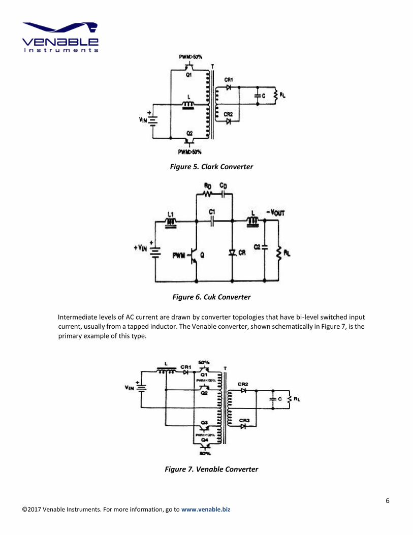
Figure 5. Clark Converter
Figure 6. Cuk Converter
Intermediate levels of AC current are drawn by converter topologies that have bi-level switched input
current, usually from a tapped inductor. The Venable converter, shown schematically in Figure 7, is the
primary example of this type.
Figure 7. Venable Converter
7
©2017 Venable Instruments. For more information, go to www.venable.biz
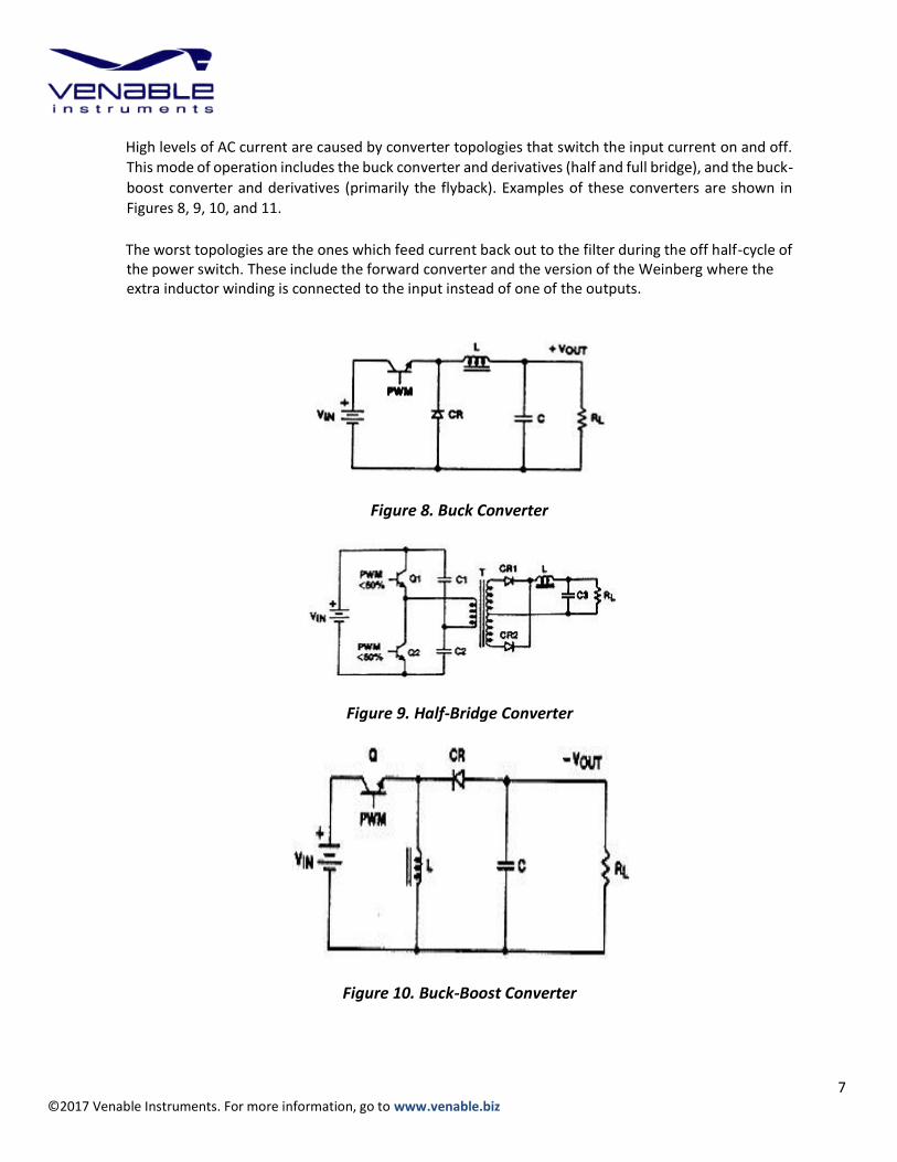
High levels of AC current are caused by converter topologies that switch the input current on and off.
This mode of operation includes the buck converter and derivatives (half and full bridge), and the buck-
boost converter and derivatives (primarily the flyback). Examples of these converters are shown in
Figures 8, 9, 10, and 11.
The worst topologies are the ones which feed current back out to the filter during the off half-cycle of the power switch. These include the forward converter and the version of the Weinberg where the extra inductor winding is connected to the input instead of one of the outputs.
Figure 8. Buck Converter
Figure 9. Half-Bridge Converter
Figure 10. Buck-Boost Converter

8
©2017 Venable Instruments. For more information, go to www.venable.biz
Figure 11. Flyback Converter
Reduce Input-Output Transfer Function
The other aspect of filter performance, other than reducing emissions, is to aid in meeting susceptibility
requirements. An alternative to attenuating the AC level of the power bus is to reduce the effect of
input voltage changes on the operating point of the converter. This has the effect of reducing the input-
to-output transfer function of the converter, so that higher levels of AC can be tolerated on the input
without causing the outputs to exceed the specification. Three methods of accomplishing a reduction of the input-to-output transfer function are available. One
is to use voltage-mode control with a circuit that changes the ramp slope to match the input voltage.
If the effective peak-to-peak voltage of the comparator ramp is proportional to input voltage, the effect
of input voltage on operating point is essentially eliminated and the supply can tolerate large AC input
without harmful effects. This mode of operation has been implemented on several commercially
available PWM control chips, notably the Unitrode UC1840.
A similar phenomenon occurs with current- mode control when the slope compensation has a value of
m = -m2/2. If the duty cycle is limited to a value significantly less than one, this can be an effective way
to reduce the susceptibility of the supply to AC voltage on its input. Figure 12 shows inductor current
in a current- mode converter with slope compensation of m = -m2/2 and various input voltages.
Figure 12. Current-Mode Control with Slope Compensation m = -m2/2

9
©2017 Venable Instruments. For more information, go to www.venable.biz
The third method of reducing susceptibility is by changing to a fixed off-time mode of operation. This
works for voltage-mode and current-mode control methods. Figure 13 shows the current waveform
for this operating mode of a current-mode converter as the input voltage is changed abruptly.
Figure 13. Fixed Off Time Mode
Optimize The Control Loop
The final step in minimizing input filter requirements is optimizing the power supply feedback control
loop for the highest possible gain and bandwidth. While this process will not help emissions, it aids in
meeting susceptibility requirements. The size and weight of the filter can be reduced if the resonant
frequency can be increased. The filter must "cut in", or start attenuating, before the feedback control
loop stops actively rejecting noise. This means that the filter corner frequency must be below the
bandwidth of the feedback control loop. Figure 14 shows this relationship between filter corner
frequency and loop bandwidth. If the filter corner frequency is close to, or especially if it is above the
loop bandwidth, there will be a range of frequencies where input noise is not rejected by the loop or
attenuated by the filter, and the supply will probably not meet conducted susceptibility requirements.
If the filter corner frequency is far below the loop bandwidth, the supply will easily meet the conducted
susceptibility requirements, but the filter will be larger, heavier, and more costly than necessary. The
objective is to make the loop bandwidth as high as possible, and then design the minimum filter, which
will still allow the outputs of the supply to stay in specification when the input is subjected to the AC
voltages defined in MIL-STD-461 or other applicable specifications.

10
©2017 Venable Instruments. For more information, go to www.venable.biz
Figure 14. Place Input Filter Corner Below Loop Gain Crossover
Keep Filter Zout Below Converter Zin
The final system design consideration is to keep the peak of the output impedance of the input filter below the dip of the input impedance of the converter. Figure 15 shows curves of impedance vs. frequency for filter output and converter input for a well-designed system. The upper curve is the converter input impedance and the lower curve is the input filter output impedance. The converter input impedance is negative, and there the combination of the input filter output impedance and the converter input impedance could be negative, causing the input filter to oscillate. The two curves should be well separated.
Figure 15. Keep Filter Zout Peak Below Converter Zin Dip

11
©2017 Venable Instruments. For more information, go to www.venable.biz
Designing The Filter
A Good, Workable Filter
The simple filter shown Figure 1 is not adequate for most military applications. A good filter topology
that is usable in many instances is shown in Figure 16.
Figure 16. Good Input Filter
This is a single-section filter in which the gain falls at a slope of 40 dB/decade, at least up to the
frequency at which the parasitic ESR of the capacitor begins to dominate. A series R-C network has
been added in parallel with the capacitor of the simple filter. The effect of this network is to reduce
the Q of the filter, reducing the peaking and output impedance.
The purpose of resistor R is to damp the filter, and the purpose of the capacitor in series with it is to
block the DC portion of the input voltage to reduce dissipation in the resistor. The blocking capacitor
must be larger than the filter capacitor since its impedance must be negligible (or at least tolerable) at
the L-C resonance. A good compromise between residual impedance of the blocking capacitor at the
damping frequency and overall size and cost of the filter is to make the blocking capacitor four times
the capacitance of the filter capacitor. This does not always mean a four times penalty in size, however.
The blocking capacitor does not have to be nearly as good quality as the filter capacitor, since there is
a resistor in series with it anyway and the blocking capacitor ESR can be compensated for simply by
reducing the value of the damping resistor an equivalent amount. Equations (2) and (3) give the
formulas for filter gain and output impedance in terms of all component values. C2 is labeled 4C in
Figure 16. Exact values can be computed from the formulas, but using the ratios specified in Figure 16
gives results that are reasonably optimized. Figure 17 shows the transfer function of Good Filter (gain)
of the filter with the circuit values specified in Figure 16, and Figure 18 is a plot of output impedance
vs. frequency for the same filter components.
Equation 2.

12
©2017 Venable Instruments. For more information, go to www.venable.biz
Equation 3.
Figure 17. Transfer Function of Good Filter
Figure 18. Output Impedance of Good Filter

13
©2017 Venable Instruments. For more information, go to www.venable.biz
A Better Filter
A single section filter may be inadequate to meet the specifications, especially if the effects of parasitics
are accounted for. A two-stage filter that is well adapted for power supplies is shown in Figure 19.
Above the resonant frequency, the gain falls off at a 60-dB/decade slope, or 80 dB/decade if the
optional small inductor is included. The damping resistor can be wire-wound, since inductance in series
actually helps the action of the filter.
Figure 19. A Better Input Filter
Phelps [2] has calculated the optimum ratio of capacitors to be C and 4C and the ratio of inductors to
be L and 6L. The exact values can be computed from the formulas (4) and (5) below. In the formulas,
the capacitor labeled 4C in Figure 19 is called C2 and the inductor labeled 6L is called L2. The small
optional inductor is called L3. If inductor L3 is not used, simply delete all terms that contain L3. The
resistor is chosen to provide minimum peaking and output impedance with these ratios of component
values. For the same total component values used in the filter of section 5.1, the attenuation of this
filter is similar near resonance, but the output impedance is significantly better. Figure 20 is a plot of
gain and Figure 21 shows the output impedance as a function of frequency. The capacitor values are
the same in both the "good" and "better" cases, but in the "better" case the original inductor has been
split into two pieces, L and 6L, which are 1/7 and 6/7 of the original value respectively.
Formula 4.

14
©2017 Venable Instruments. For more information, go to www.venable.biz
Formula 5.
MIL-STD-461
MIL-STD-461 is the controlling document for emission and susceptibility requirements for electronic
equipment purchased by the Department of Defense. It is a comprehensive document, but two limit
curves define most of the requirements for equipment operating from a DC bus. There are nine classes
of equipment and each class has different specifications. The examples shown below are for class 2,
aircraft equipment.
Figure 20. Transfer Function of Better Filter

15
©2017 Venable Instruments. For more information, go to www.venable.biz
Figure 21. Output Impedance of Better Filter
CS01 Susceptibility Limits
CS01 defines the limits of AC voltage that is superimposed on the DC power bus for test purposes.
The frequency limits of this curve are 30 Hz to 50 kHz. The voltage limits are shown in Figure 22.
Figure 22. CS01 Susceptibility Limits for Airborne Equipment
Below 30 Hz, the loop should be rejecting almost all of the AC input voltage. Above 50 kHz, the input
filter should attenuate the input voltage to a negligible level. At intermediate frequencies, typically
somewhere between 100 Hz and 10 kHz, the interface between loop rejection and filter attenuation
takes place, and that is the frequency where problems will occur unless care is taken in the design to
maximize loop crossover frequency and filter attenuation.

16
©2017 Venable Instruments. For more information, go to www.venable.biz
CE03 Emission Limits
CE03 defines the limits of current that can be put back on the power bus in the frequency range of 15
kHz to 50 MHz. The limits are shown in Figure 23. This is a narrowband specification. There are also
lower frequency and broadband specifications, but CE03 is the most applicable. Most switching power
supplies operate at frequencies of 20 kHz to 200 kHz, and a few up to 1 MHz. There is no emission at
frequencies below the switching frequency. Emissions are primarily at the fundamental and harmonics
of the switching frequency, and that is why the narrowband specification is most applicable. These
current harmonics have to be attenuated by the reverse current filter action of the input filter to levels
below the CE03 limits. The final filter design must incorporate both susceptibility and emission
requirements and must be effective enough to meet both specifications simultaneously.
Figure 23. CE03 Emission Limits for Airborne Equipment
Typical Filter Performance
Closed-Loop Transfer Function
This section describes typical filter characteristics and the effects of the input filter on conducted
susceptibility and loop transfer function. Figure 24 shows the transfer function (gain) of a typical input
filter. Input AC voltage is passed through without attenuation up to the corner frequency of the filter.
There is typically some peaking at the corner, and then the gain falls off at a slope de- pendent on the
particular filter topology selected, typically 40 to 80 dB/decade.
Figure 24. Transfer Function of Typical Well-Damped Input Filter

17
©2017 Venable Instruments. For more information, go to www.venable.biz
Figure 25 shows a typical input-to-output transfer function of a power supply without an input filter.
The loop attenuates low frequencies, but as the loop gain decreases an increasing amount of the input
AC passes through the supply. This particular example has a well-designed loop that crosses over above
the corner frequency of the output filter. At high frequency, attenuation comes from the output filter.
Figure 25. Input-to-Output Transfer Function of a Supply
In many cases the designer has taken the easy way out in control loop design and crossed the loop over
below the corner of the output L-C filter. In this case, there is a range of frequencies where neither the
loop nor the output filter is attenuates the input AC voltage, and the input filter has a monumental job
reducing the AC voltage to an acceptable level. It must do the job without help from the supply itself,
and must have a much lower corner frequency with attendant increases in size, weight, and cost. When
the input filter and power supply are combined, the net result is a transfer function, which is essentially
the product of the filter and power supply transfer functions. Figure 26 shows the overall transfer
function that resulted from combining the filter and power supply transfer functions of Figures 24 and
25 respectively. There is still a peak at the intermediate frequencies, but the levels have been reduced
to the point where they pose no problem for the using equipment.
Figure 26. Input-to-Output Transfer Function with Input Filter

18
©2017 Venable Instruments. For more information, go to www.venable.biz
Open-Loop Gain
The filter does have an impact on open loop gain. In most control methods, the control-tooutput transfer function is proportional to input voltage. At the resonance of the input filter, the filter is parallel resonant from an output impedance standpoint, and presents a high source impedance for AC current. Drawing current at this frequency drops the input voltage to the power supply, reducing the control-to-output transfer function and causing a dip in open-loop gain. The size of the dip is related to the input filter Q, and if the Q is high, the dip can be significant. Figure 27 shows the open-loop gain of a typical power supply without an input filter. The curve is well
behaved and has a crossover frequency of 3 kHz and a phase margin of 60 degrees. Figure 28 shows the open-loop gain of the same supply with a relatively high-Q input filter. There is a significant gain dip, which actually reduces the gain below unity. There is a related phase variation that dips and then rises. The phase does not dip quite to the 0 degree (really 360 degree) axis, but if it had the loop would have oscillated at that frequency. If subjected to a load transient, this supply will ring at the input filter resonant frequency, even though true loop crossover is still 3 kHz and the phase margin is still 60 degrees, resulting in almost ideal response of the true loop. This is an excellent example of why transient response testing is not an adequate method of testing feedback loop characteristics and performance.
Figure 27. Open-Loop Gain and Phase With No Input Filter
Figure 28. Open-Loop Gain and Phase With Undamped Input Filter

19
©2017 Venable Instruments. For more information, go to www.venable.biz
By proper damping as discussed earlier, the open-loop gain characteristic can be returned almost to
the pristine state it had before the filter was added. Figure 29 shows the open-loop gain of the same
supply with optimum damping of the input filter. There are still residual effects of the filter, but they
are well within acceptable limits and the performance of the power supply is not degraded. If the
supply is to be subjected to full military temperature extremes, care must be taken to assure that the
filter and damping capacitors still function as intended at the extreme low limits of temperature.
Figure 29. Open-Loop Gain and Phase With Well-Damped Input Filter
Summary
To minimize input filter requirements, choose a topology that has a minimum AC input current content. Then choose an operating mode that minimizes the input- to-output transfer function. These two choices dramatically affect the size and weight of the filter required to meet the emissions and susceptibility requirements of MIL-STD-461.
After selecting the topology and operating mode, optimize the bandwidth of the feedback control loop, being sure to have the bandwidth above the resonant frequency of the power supply output filter. Design the input filter to meet CS01 and CE03, and be sure to provide adequate damping. After the design is finished, calculate or preferably measure the result and the effect on the feedback control loop. By following these simple step-by- step guidelines the size, weight, and cost of input filters can be greatly reduced.
References
1. R. D. Middlebrook, "Design Techniques for Preventing Input Filter Oscillations in Switched-Mode Regulators," Proceedings of the Fifth National Solid-State Power Conversion Conference, Powercon 5, pp. A3-1 through A3-16, May 1978.
2. T. K. Phelps and W. S. Tate, "Optimizing Passive Input Filter Design," Proceedings of the Sixth
National Solid- State Power Conversion Conference, Powercon 6, pp. G1-1 through G1-10, May 1979.