Application Note - Leica Microsystems EM... · Application Note Carbon Coating for Polymeric...
5
Application Note Carbon Coating for Polymeric Materials related instruments: Leica EM ACE600 Material Research Life Science Research Medical Research Industrial Manufacturing Natural Resources
Transcript of Application Note - Leica Microsystems EM... · Application Note Carbon Coating for Polymeric...

Application Note Carbon Coating for Polymeric Materialsrelated instruments: Leica EM ACE600
Material
Research
Life Science
Research
Medical
Research
Industrial
Manufacturing
Natural
Resources

Carbon Coating for Polymeric Materials
A solid understanding of polymer property-structure relationships is critical to improve and shorten development routes to new
products. A direct way to determine correlations between structure and mechanical properties is provided by electron microscopy.
Electron microscopy techniques have an important advantage over other methods, as they can provide local information at high spatial
resolution. However, a major problem with polymers is their inherent lack of contrast. The contrast between structural details is often
too low because polymers usually consist of the same light elements that interact only weakly with the electron beam. Moreover,
beam damage, sample preparation and imaging artefacts are often hampering a straightforward analysis and a correct interpretation.
HAADF-STEM (High Angle Annular Dark Field Scanning TEM) presents the most effective mode for imaging nanoscale organization of
polymeric materials provided that they have phases with different densities and/or atomic weight. In contrast to conventional BF-TEM,
HAADF-STEM images do not possess phase contrast and have a higher signal-to-noise ratio. The incoherent nature of the HAADF-
STEM signals provide images that can be interpreted in a straightforward manner. In cases where different phases are similar in terms
of atomic weight or density, selective staining or EELS-fingerprinting can be used.
For this application note, supramolecular thermoplastic materials, consisting of mixtures of oppositely charged oligomeric ABA-type
triblock copolymers (DMAEA-BA-DMAEA and CEA-BA-CEA) were investigated.
Ultrathin sections of 60 nm were obtained by cryosectioning at -80°C using a Leica EM UC7 microtome equipped with a Leica EM FC7
cryochamber (image 1). A micromanipulator and electrostatic charger were used to attach ribbons of sections on a Quantifoil grid
(image 2, 3). The samples were vapor stained with osmium tetroxide (2%) for 30 minutes. OsO4 selectively stains the charged phase
(DMAEA-CEA domains) in the polymeric material. The obtained TEM grids were coated with a 2 nanometer thick amorphous carbon
layer at both sides using a Leica EM ACE600 high vacuum coater. This improves heat dissipation, charging and mass loss during
subsequent imaging.
2

Imaging was only performed in those parts of the stained sections that cover the holes in the carbon film (image 4). When BF-TEM is
used (image 5), a strong phase contrast and a poor SNR impede a clear observation of the morphology. HAADF-STEM (image 6, 7) on
the other hand, clearly resolves the nanoscale phase separation (charged domains are bright). Here, OsO4 only interacts at the surface
of the section. Sections (image 6, 7) along two perpendicular planes of the same material show an identical morphology.
HAADF-STEM images of different materials are shown in images 8-11. They all exhibit a nano-phase separated morphology. Mix 1
(image 8) shows dispersed charged DMAEA-CEA domains of spherical shape randomly distributed in space, as confirmed with Fourier
transform (FT) of the HAADF-STEM image (see inset of image 8). The characteristic size of the dispersed domains is 6.7 ± 1.1 nm. Mix
2 (image 9) shows curled bundles of hexagonally packed cylinders of the charged DMAEA-CEA phase. The inset at the bottom of image
9 is demonstrating the nearly close-packed hexagonal arrangement of the cylinders of DMAEA-CEA. The upper inset shows a FT of the
HAADF-STEM image and provides a direct comparison with the SANS diffractogram shown in image 13.
3LNT Application Note - CARBON COATING FOR POLYMERIC MATERIALS
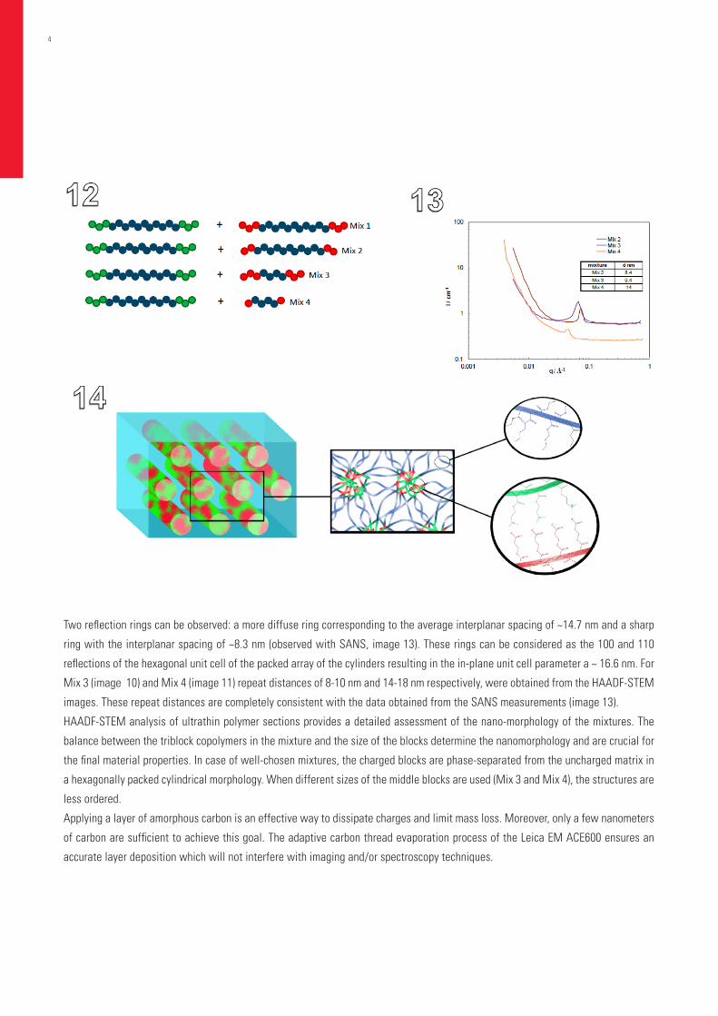
Two reflection rings can be observed: a more diffuse ring corresponding to the average interplanar spacing of ~14.7 nm and a sharp
ring with the interplanar spacing of ~8.3 nm (observed with SANS, image 13). These rings can be considered as the 100 and 110
reflections of the hexagonal unit cell of the packed array of the cylinders resulting in the in-plane unit cell parameter a ~ 16.6 nm. For
Mix 3 (image 10) and Mix 4 (image 11) repeat distances of 8-10 nm and 14-18 nm respectively, were obtained from the HAADF-STEM
images. These repeat distances are completely consistent with the data obtained from the SANS measurements (image 13).
HAADF-STEM analysis of ultrathin polymer sections provides a detailed assessment of the nano-morphology of the mixtures. The
balance between the triblock copolymers in the mixture and the size of the blocks determine the nanomorphology and are crucial for
the final material properties. In case of well-chosen mixtures, the charged blocks are phase-separated from the uncharged matrix in
a hexagonally packed cylindrical morphology. When different sizes of the middle blocks are used (Mix 3 and Mix 4), the structures are
less ordered.
Applying a layer of amorphous carbon is an effective way to dissipate charges and limit mass loss. Moreover, only a few nanometers
of carbon are sufficient to achieve this goal. The adaptive carbon thread evaporation process of the Leica EM ACE600 ensures an
accurate layer deposition which will not interfere with imaging and/or spectroscopy techniques.
4

RELATED PRODUCTS
Leica EM ACE600
Leic
a EM
ACE
600
App
licat
ion
Not
e C
ARB
ON
CO
ATI
NG
FO
R PO
LYM
ERIC
MA
TERI
ALS
∙11/
16 ∙
Copy
righ
t © b
y Le
ica
Mik
rosy
stem
e G
mbH
, Vie
nna,
Aus
tria
, 201
5. S
ubje
ct to
mod
ifica
tions
. LEI
CA
and
the
Leic
a Lo
go a
re re
gist
ered
trad
emar
ks o
f Lei
ca M
icro
syst
ems
IR G
mbH
.
Leica Mikrosysteme GmbH | Vienna, Austria
T +43 1 486 8050-0 | F +43 1 486 8050-30
www.leica-microsystems.com
CONNECT WITH US!