AP0100CS High-Dynamic Range (HDR) Image Signal Processor …
50
© Semiconductor Components Industries, LLC, 2016 October, 2018 − Rev. 7 1 Publication Order Number: AP0100CS/D AP0100CS AP0100CS High-Dynamic Range (HDR) Image Signal Processor (ISP) General Description The ON Semiconductor AP0100CS is a high−performance, ultra−low power in−line, digital image processor optimized for use with High Dynamic Range (HDR) sensors. The AP0100CS provides full auto−functions support (AWB and AE) and Adaptive Local Tone Mapping (ALTM) to enhance HDR images and advanced noise reduction which enables excellent low−light performance. Table 1. KEY PERFORMANCE PARAMETERS Parameter Value Primary camera interfaces Parallel and HiSPi Primary camera input RAW12 Linear/RAW12, RAW14 (HiSPi format only) Companded Output interface Analog composite, up to 16−bit parallel digital output Output format YUV422 8−bit,10−bit, and 10−, 12−bit tone−mapped Bayer Maximum resolution 1280 × 960 (1.2 Mp) NTSC Output 720H × 487V PAL Output 720H × 576V Input clock range 6−30 MHz Supply voltage V DD IO_S 1.8 or 2.8 V nominal V DD IO_H 2.5 or 3.3 V nominal V DD _REG 1.8 V nominal V DD 1.2 V nominal V DD _PLL 1.2 V nominal V DD _DAC 1.2 V nominal V DD IO_OTPM 2.5 or 3.3 V nominal V DD A_DAC 3.3 V nominal V DD _PHY 2.8 V nominal Operating temp. −30°C to + 70°C Power consumption 185 mW Features • Up to 1.2 Mp (1280 x 960) ON Semiconductor sensor support • 45 fps at 1.2 Mp, 60 fps at 720 p • Optimized for operation with HDR sensors • Color and gamma correction • Auto exposure, auto white balance, 50/60 Hz auto flicker detection and avoidance • Adaptive Local Tone Mapping (ALTM) www. onsemi.com MARKING DIAGRAM XXXXXXXXXXX = Laser Marking See detailed ordering and shipping information on page 2 of this data sheet. ORDERING INFORMATION • Programmable Spatial Transform Engine (STE) • Pre−rendered Graphical Overlay • Two−wire serial programming interface (CCIS) • Interface to low−cost Flash or EPROM through SPI bus (to configure and load patches, etc.) • High−level host command interface • Standalone operation supported • Up to 5 GPIO • Fail−safe IO • Multi−Camera synchronization support • Integrated video encoder for NTSC/PAL with overlay capability and 10−bit I−DAC • SMPTE296 HDCCTV cameras • Surveillance network IP cameras Applications BALL A1 ID VFBGA100, 7x7 CASE 138AH
Transcript of AP0100CS High-Dynamic Range (HDR) Image Signal Processor …

© Semiconductor Components Industries, LLC, 2016
October, 2018 − Rev. 71 Publication Order Number:
AP0100CS/D
AP0100CS
AP0100CS High-DynamicRange (HDR) Image SignalProcessor (ISP)General Description
The ON Semiconductor AP0100CS is a high−performance,ultra−low power in−line, digital image processor optimized for usewith High Dynamic Range (HDR) sensors. The AP0100CS providesfull auto−functions support (AWB and AE) and Adaptive Local ToneMapping (ALTM) to enhance HDR images and advanced noisereduction which enables excellent low−light performance.
Table 1. KEY PERFORMANCE PARAMETERS
Parameter Value
Primary camera interfaces Parallel and HiSPi
Primary camera input RAW12 Linear/RAW12, RAW14 (HiSPiformat only) Companded
Output interface Analog composite, up to 16−bit paralleldigital output
Output format YUV422 8−bit,10−bit, and 10−, 12−bittone−mapped Bayer
Maximum resolution 1280 × 960 (1.2 Mp)
NTSC Output 720H × 487V
PAL Output 720H × 576V
Input clock range 6−30 MHz
Supply voltage VDDIO_S 1.8 or 2.8 V nominal
VDDIO_H 2.5 or 3.3 V nominal
VDD_REG 1.8 V nominal
VDD 1.2 V nominal
VDD_PLL 1.2 V nominal
VDD_DAC 1.2 V nominal
VDDIO_OTPM 2.5 or 3.3 V nominal
VDDA_DAC 3.3 V nominal
VDD_PHY 2.8 V nominal
Operating temp. −30°C to + 70°C
Power consumption 185 mW
Features• Up to 1.2 Mp (1280 x 960) ON Semiconductor sensor support
• 45 fps at 1.2 Mp, 60 fps at 720 p
• Optimized for operation with HDR sensors
• Color and gamma correction
• Auto exposure, auto white balance, 50/60 Hz auto flicker detectionand avoidance
• Adaptive Local Tone Mapping (ALTM)
www.onsemi.com
MARKING DIAGRAM
XXXXXXXXXXX = Laser Marking
See detailed ordering and shipping information on page 2 ofthis data sheet.
ORDERING INFORMATION
• Programmable Spatial Transform Engine(STE)
• Pre−rendered Graphical Overlay
• Two−wire serial programming interface(CCIS)
• Interface to low−cost Flash or EPROMthrough SPI bus (to configure and loadpatches, etc.)
• High−level host command interface
• Standalone operation supported
• Up to 5 GPIO
• Fail−safe IO
• Multi−Camera synchronization support
• Integrated video encoder for NTSC/PALwith overlay capability and 10−bit I−DAC
• SMPTE296 HDCCTV cameras
• Surveillance network IP cameras
Applications
BALL A1 ID
VFBGA100, 7x7CASE 138AH
AP0100CS
www.onsemi.com2
ORDERING INFORMATION
Table 2. AVAILABLE PART NUMBERS
Part Number Product Description Orderable Product Attribute Description
AP0100CS2L00SUGA0−DR1 1Mp Co−Processor, 100−ball VFBGA Drypack
AP0100CS2L00SPGAD3−GEVK AP0100CS Demo Kit
AP0100CS2L00SPGAH−GEVB AP0100CS Head Board
1. See the ON Semiconductor Device Nomenclature document (TND310/D) for a full description of the naming convention used for imagesensors. For reference documentation, including information on evaluation kits, please visit our web site at www.onsemi.com.
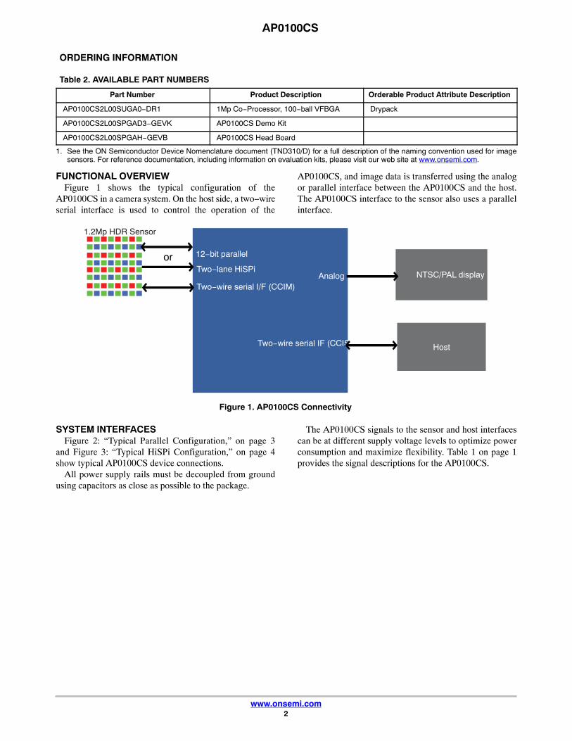
FUNCTIONAL OVERVIEWFigure 1 shows the typical configuration of the
AP0100CS in a camera system. On the host side, a two−wireserial interface is used to control the operation of the
AP0100CS, and image data is transferred using the analogor parallel interface between the AP0100CS and the host.The AP0100CS interface to the sensor also uses a parallelinterface.
Figure 1. AP0100CS Connectivity
1.2Mp HDR Sensor
12−bit parallel
Host
Two−wire serial I/F (CCIM)
Two−wire serial IF (CCIS)
Two−lane HiSPior
Analog NTSC/PAL display
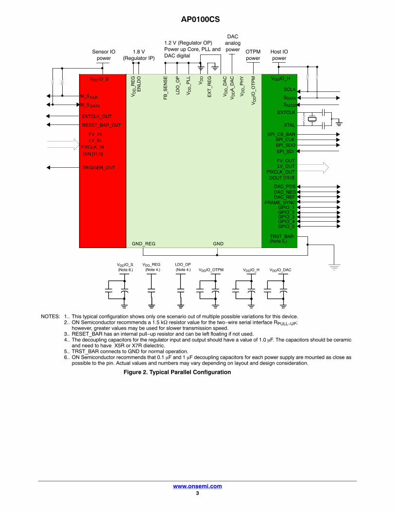
SYSTEM INTERFACESFigure 2: “Typical Parallel Configuration,” on page 3
and Figure 3: “Typical HiSPi Configuration,” on page 4show typical AP0100CS device connections.
All power supply rails must be decoupled from groundusing capacitors as close as possible to the package.
The AP0100CS signals to the sensor and host interfacescan be at different supply voltage levels to optimize powerconsumption and maximize flexibility. Table 1 on page 1provides the signal descriptions for the AP0100CS.
AP0100CS
www.onsemi.com3
VDDIO_S(Note 6.)
VDD_REG(Note 4.)
LDO_OP(Note 4.) VDDIO_OTPM VDDIO_H
NOTES: 1.. This typical configuration shows only one scenario out of multiple possible variations for this device.2.. ON Semiconductor recommends a 1.5 k� resistor value for the two−wire serial interface RPULL−UP;
however, greater values may be used for slower transmission speed.3.. RESET_BAR has an internal pull−up resistor and can be left floating if not used.4.. The decoupling capacitors for the regulator input and output should have a value of 1.0 �F. The capacitors should be ceramic
and need to have X5R or X7R dielectric.5.. TRST_BAR connects to GND for normal operation.6.. ON Semiconductor recommends that 0.1 �F and 1 �F decoupling capacitors for each power supply are mounted as close as
possible to the pin. Actual values and numbers may vary depending on layout and design consideration.
VDDIO_S VDDIO_H
M_S CLK
M_S DATA
EXTCLK_OUT
RESET_BAR_OUT
DIN [11:0]
TRIGGER_OUT
GND_REG
FV_OUT
DOUT [15:0]
SCLK
EXTCLK
XTAL
SPI_CS_BAR
SPI_SDI
GPIO_1
TRST_BAR
GND
GPIO_2GPIO_3GPIO_4GPIO_5
FRAME_SYNC
FV_INLV_IN
PIXCLK_IN
1.8 V(Regulator IP)
Sensor IOpower
1.2 V (Regulator OP)Power up Core, PLL andDAC digital
OTPMpower
Host IOpower
SDATA
SADDR
LV_OUTPIXCLK_OUT
(Note 5.)
SPI_CLKSPI_SDO
VD
D_R
EG
EN
LDO
VD
DIO
_OT
PM
VD
D_P
HY
VD
DA
_DA
C
VD
D_D
AC
FB
_SE
NS
E
LDO
_OP
VD
D_P
LL
VD
D
EX
T_R
EG
DACanalogpower
DAC_POSDAC_NEGDAC_REF
VDDIO_DAC
Figure 2. Typical Parallel Configuration
AP0100CS
www.onsemi.com4
LDO
_OP
Figure 3. Typical HiSPi Configuration
VDDIO_S(Note 8.)
VDD_REG(Note 7.)
LDO_OP(Note 7.) VDDIO_OTPM VDDIO_H
VDDIO_S VDDIO_H
M_S CLK
M_S DATA
EXTCLK_OUT
RESET_BAR_OUT
DIN [11:0]
TRIGGER_OUT
GND_REG
FV_OUT
DOUT [15:0]
SCLK
EXTCLK
XTAL
SPI_CS_BAR
SPI_SDI
GPIO_1
TRST_BAR
GND
GPIO_2GPIO_3GPIO_4GPIO_5
FRAME_SYNC
FV_INLV_IN
PIXCLK_IN
1.8 V(Regulator IP)
Sensor IOpower
1.2 V (Regulator OP)Power up Core, PLL andDAC digital
OTPMpower
Host IOpower
SDATA
SADDR
LV_OUTPIXCLK_OUT
(Note 5.)
SPI_CLKSPI_SDO
VD
D_R
EG
EN
LDO
VD
DIO
_OT
PM
VD
D_P
HY
VD
DA
_DA
C
VD
D_D
AC
FB
_SE
NS
E
VD
D_P
LL
VD
D
CLK_N CLK_P
DACanalogpower
DAC_POSDAC_NEGDAC_REF
VDDIO_DAC
DATA0_N DATA0_PDATA1_N DATA1_P
DACanalogpower
DACanalogpower
Sensor IOpower
VDDIO_PHY
NOTES: 7.. The decoupling capacitors for the regulator input and output should have a value of 1.0 �F. The capacitors should be ceramicand need to have X5R or X7R dielectric.
8.. ON Semiconductor recommends that 0.1 �F and 1 �F decoupling capacitors for each power supply are mounted as close aspossible to the pin. Actual values and numbers may vary depending on layout and design consideration.
HiSPi and Parallel ConnectionWhen using the HiSPi interface, the user should connect
the parallel interface to VDDIO_S. When using the parallelinterface, the HiSPi interface and power supply(VDD_PHY) can be left floating.
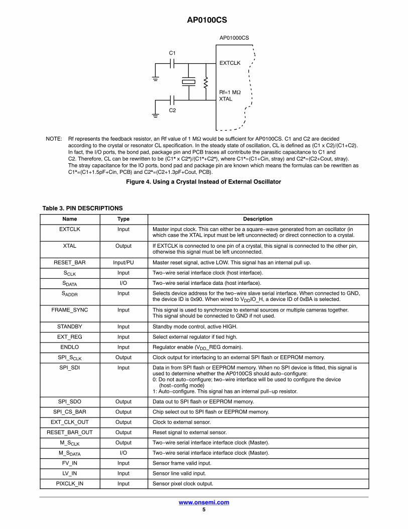
Crystal UsageAs an alternative to using an external oscillator, a crystal
may be connected between EXTCLK and XTAL. Two smallloading capacitors and a feedback resistor should be added,as shown in Figure 4.
AP0100CS
www.onsemi.com5
C1
C2
AP01000CS
EXTCLK
Rf=1 M�
XTAL
NOTE: Rf represents the feedback resistor, an Rf value of 1 M� would be sufficient for AP0100CS. C1 and C2 are decidedaccording to the crystal or resonator CL specification. In the steady state of oscillation, CL is defined as (C1 x C2)/(C1+C2).In fact, the I/O ports, the bond pad, package pin and PCB traces all contribute the parasitic capacitance to C1 andC2. Therefore, CL can be rewritten to be (C1* x C2*)/(C1*+C2*), where C1*=(C1+Cin, stray) and C2*=(C2+Cout, stray).The stray capacitance for the IO ports, bond pad and package pin are known which means the formulas can be rewritten asC1*=(C1+1.5pF+Cin, PCB) and C2*=(C2+1.3pF+Cout, PCB).
Figure 4. Using a Crystal Instead of External Oscillator
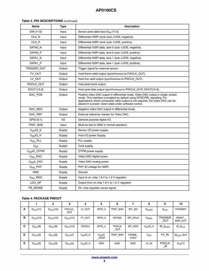
Table 3. PIN DESCRIPTIONS
Name Type Description
EXTCLK Input Master input clock. This can either be a square−wave generated from an oscillator (inwhich case the XTAL input must be left unconnected) or direct connection to a crystal.
XTAL Output If EXTCLK is connected to one pin of a crystal, this signal is connected to the other pin,otherwise this signal must be left unconnected.
RESET_BAR Input/PU Master reset signal, active LOW. This signal has an internal pull up.
SCLK Input Two−wire serial interface clock (host interface).
SDATA I/O Two−wire serial interface data (host interface).
SADDR Input Selects device address for the two−wire slave serial interface. When connected to GND,the device ID is 0x90. When wired to VDDIO_H, a device ID of 0xBA is selected.
FRAME_SYNC Input This signal is used to synchronize to external sources or multiple cameras together.This signal should be connected to GND if not used.
STANDBY Input Standby mode control, active HIGH.
EXT_REG Input Select external regulator if tied high.
ENDLO Input Regulator enable (VDD_REG domain).
SPI_SCLK Output Clock output for interfacing to an external SPI flash or EEPROM memory.
SPI_SDI Input Data in from SPI flash or EEPROM memory. When no SPI device is fitted, this signal isused to determine whether the AP0100CS should auto−configure:0: Do not auto−configure; two−wire interface will be used to configure the device
(host−config mode)1: Auto−configure. This signal has an internal pull−up resistor.
SPI_SDO Output Data out to SPI flash or EEPROM memory.
SPI_CS_BAR Output Chip select out to SPI flash or EEPROM memory.
EXT_CLK_OUT Output Clock to external sensor.
RESET_BAR_OUT Output Reset signal to external sensor.
M_SCLK Output Two−wire serial interface interface clock (Master).
M_SDATA I/O Two−wire serial interface interface clock (Master).
FV_IN Input Sensor frame valid input.
LV_IN Input Sensor line valid input.
PIXCLK_IN Input Sensor pixel clock output.
AP0100CS
www.onsemi.com6
Table 3. PIN DESCRIPTIONS (continued)
Name DescriptionType
DIN [11:0] Input Sensor pixel data input DIN [11:0].
CLK_N Input Differential HiSPi clock (sub−LVDS, negative).
CLK_P Input Differential HiSPi clock (sub−LVDS, positive).
DATA0_N Input Differential HiSPi data, lane 0 (sub−LVDS, negative).
DATA0_P Input Differential HiSPi data, lane 0 (sub−LVDS, positive).
DATA1_N Input Differential HiSPi data, lane 1 (sub−LVDS, negative).
DATA1_P Input Differential HiSPi data, lane 1 (sub−LVDS, positive).
TRIGGER_OUT Output Trigger signal for external sensor.
FV_OUT Output Host frame valid output (synchronous to PIXCLK_OUT).
LV_OUT Output Host line valid output (synchronous to PIXCLK_OUT).
PIXCLK_OUT Output Host pixel clock output.
DOUT [15:0] Output Host pixel data output (synchronous to PIXCLK_OUT) DOUT[15:0].
DAC_POS Output Positive video DAC output in differential mode. Video DAC output in single−endedmode. This interface is enabled by default using NTSC/PAL signaling. Forapplications where composite video output is not required, the video DAC can beplaced in a power−down state under software control.
DAC_NEG Output Negative video DAC output in differential mode.
DAC_REF Output External reference resistor for Video DAC.
GPIO [5:1] I/O General purpose digital I/O.
TRST_BAR Input Must be tied to GND in normal operation.
VDDIO_S Supply Sensor I/O power supply.
VDDIO_H Supply Host I/O power Supply.
VDD_PLL Supply PLL supply.
VDD Supply Core supply.
VDDIO_OTPM Supply OTPM power supply.
VDD_DAC Supply Video DAC digital power.
VDDA_DAC Supply Video DAC analog power.
VDD_PHY Supply PHY IO voltage for HiSPi.
GND Supply Ground.
VDD_REG Supply Input to on−chip 1.8 V to 1.2 V regulator.
LDO_OP Supply Output from on chip 1.8 V to 1.2 V regulator.
FB_SENSE Supply On−chip regulator sense signal.
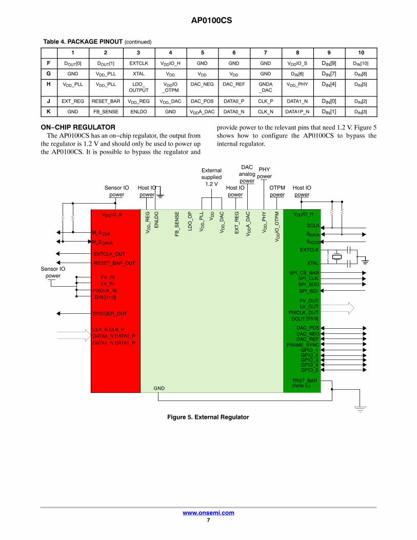
Table 4. PACKAGE PINOUT
1 2 3 4 5 6 7 8 9 10
A DOUT[11] DOUT[13] PIXCLK_OUT
LV_OUT GPIO_2 TRST_BAR SPI_SDI SADDR SCLK STANDBY
B DOUT[12] DOUT[10] DOUT[14] FV_OUT GPIO_3 GPIO[5] SPI_SCLK SDATA TRIGGER_OUT
RESET_BAR_OUT
C DOUT[9] DOUT[8] DOUT[15] GPIO[1] GPIO_4 PIXCLK_OUT
SPI_SDO VDDIO_H M_SDATA M_SCLK
D DOUT[5] DOUT[6] DOUT[7] VDDIO_H VDDIO_HOST
TRST_BAR FRAME_SYNC
VDD FV_IN MCLK_OUT
E DOUT[2] DOUT[3] DOUT[4] VDDIO_H GND GND GND LV_IN PIXCLK_IN
DIN[11]
AP0100CS
www.onsemi.com7
Table 4. PACKAGE PINOUT (continued)
10987654321
F DOUT[0] DOUT[1] EXTCLK VDDIO_H GND GND GND VDDIO_S DIN[9] DIN[10]
G GND VDD_PLL XTAL VDD VDD VDD GND DIN[6] DIN[7] DIN[8]
H VDD_PLL VDD_PLL LDO_OUTPUT
VDDIO_OTPM
DAC_NEG DAC_REF GNDA_DAC
VDD_PHY DIN[4] DIN[5]
J EXT_REG RESET_BAR VDD_REG VDD_DAC DAC_POS DATA0_P CLK_P DATA1_N DIN[0] DIN[2]
K GND FB_SENSE ENLDO GND VDDA_DAC DATA0_N CLK_N DATA1P_N DIN[1] DIN[3]
ON−CHIP REGULATORThe AP0100CS has an on−chip regulator, the output from
the regulator is 1.2 V and should only be used to power upthe AP0100CS. It is possible to bypass the regulator and
provide power to the relevant pins that need 1.2 V. Figure 5shows how to configure the AP0100CS to bypass theinternal regulator.
Figure 5. External Regulator
VDDIO_S VDDIO_H
M_S CLK
M_S DATA
EXTCLK_OUT
RESET_BAR_OUT
DIN [11:0]
TRIGGER_OUT
FV_OUT
DOUT [15:0]
SCLK
EXTCLK
XTAL
SPI_CS_BAR
SPI_SDI
GPIO_1
TRST_BAR
GND
GPIO_2GPIO_3GPIO_4GPIO_5
FRAME_SYNC
FV_INLV_IN
PIXCLK_IN
Externalsupplied
1.2 VSensor IO
powerOTPMpower
Host IOpower
SDATA
SADDR
LV_OUTPIXCLK_OUT
(Note 5.)
SPI_CLKSPI_SDO
VD
D_R
EG
EN
LDO
VD
DIO
_OT
PM
VD
D_P
HY
VD
DA
_DA
C
VD
D_D
AC
FB
_SE
NS
E
LDO
_OP
VD
D_P
LL
VD
D
CLK_N CLK_P
DACanalogpower
DAC_POSDAC_NEGDAC_REF
DATA0_N DATA0_PDATA1_N DATA1_P
Sensor IOpower
EX
T_R
EG
Host IOpower
Host IOpower
PHYpower
AP0100CS
www.onsemi.com8
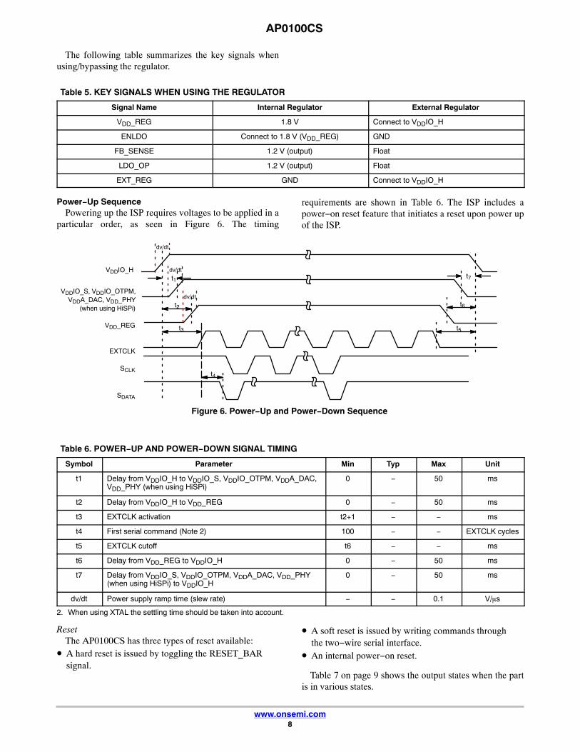
The following table summarizes the key signals whenusing/bypassing the regulator.
Table 5. KEY SIGNALS WHEN USING THE REGULATOR
Signal Name Internal Regulator External Regulator
VDD_REG 1.8 V Connect to VDDIO_H
ENLDO Connect to 1.8 V (VDD_REG) GND
FB_SENSE 1.2 V (output) Float
LDO_OP 1.2 V (output) Float
EXT_REG GND Connect to VDDIO_H
Power−Up SequencePowering up the ISP requires voltages to be applied in a
particular order, as seen in Figure 6. The timing
requirements are shown in Table 6. The ISP includes apower−on reset feature that initiates a reset upon power upof the ISP.
dv/dt
VDDIO_H
VDD_REG
EXTCLK
SCLK
SDATA
VDDIO_S, VDDIO_OTPM,VDDA_DAC, VDD_PHY
(when using HiSPi)
dv/dt
dv/dt
t1
t2
t3
t4
t5
t6
t7
Figure 6. Power−Up and Power−Down Sequence
Table 6. POWER−UP AND POWER−DOWN SIGNAL TIMING
Symbol Parameter Min Typ Max Unit
t1 Delay from VDDIO_H to VDDIO_S, VDDIO_OTPM, VDDA_DAC,VDD_PHY (when using HiSPi)
0 − 50 ms
t2 Delay from VDDIO_H to VDD_REG 0 − 50 ms
t3 EXTCLK activation t2+1 − − ms
t4 First serial command (Note 2) 100 − − EXTCLK cycles
t5 EXTCLK cutoff t6 − − ms
t6 Delay from VDD_REG to VDDIO_H 0 − 50 ms
t7 Delay from VDDIO_S, VDDIO_OTPM, VDDA_DAC, VDD_PHY(when using HiSPi) to VDDIO_H
0 − 50 ms
dv/dt Power supply ramp time (slew rate) − − 0.1 V/�s
2. When using XTAL the settling time should be taken into account.
ResetThe AP0100CS has three types of reset available:
• A hard reset is issued by toggling the RESET_BARsignal.
• A soft reset is issued by writing commands throughthe two−wire serial interface.
• An internal power−on reset.
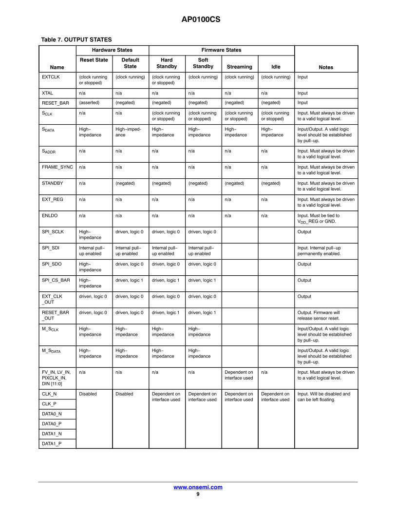
Table 7 on page 9 shows the output states when the partis in various states.
AP0100CS
www.onsemi.com9
Table 7. OUTPUT STATES
Name
Hardware States Firmware States
NotesReset State Default
StateHard
StandbySoft
Standby Streaming Idle
EXTCLK (clock runningor stopped)
(clock running) (clock runningor stopped)
(clock running) (clock running) (clock running) Input
XTAL n/a n/a n/a n/a n/a n/a Input
RESET_BAR (asserted) (negated) (negated) (negated) (negated) (negated) Input
SCLK n/a n/a (clock runningor stopped)
(clock runningor stopped)
(clock runningor stopped)
(clock runningor stopped)
Input. Must always be drivento a valid logical level.
SDATA High−impedance
High−imped-ance
High−impedance
High−impedance
High−impedance
High−impedance
Input/Output. A valid logiclevel should be establishedby pull−up.
SADDR n/a n/a n/a n/a n/a n/a Input. Must always be drivento a valid logical level.
FRAME_SYNC n/a n/a n/a n/a n/a n/a Input. Must always be drivento a valid logical level.
STANDBY n/a (negated) (negated) (negated) (negated) (negated) Input. Must always be drivento a valid logical level.
EXT_REG n/a n/a n/a n/a n/a n/a Input. Must always be drivento a valid logical level.
ENLDO n/a n/a n/a n/a n/a n/a Input. Must be tied toVDD_REG or GND.
SPI_SCLK High−impedance
driven, logic 0 driven, logic 0 driven, logic 0 Output
SPI_SDI Internal pull−up enabled
Internal pull−up enabled
Internal pull−up enabled
Internal pull−up enabled
Input. Internal pull−uppermanently enabled.
SPI_SDO High−impedance
driven, logic 0 driven, logic 0 driven, logic 0 Output
SPI_CS_BAR High−impedance
driven, logic 1 driven, logic 1 driven, logic 1 Output
EXT_CLK_OUT
driven, logic 0 driven, logic 0 driven, logic 0 driven, logic 0 Output
RESET_BAR_OUT
driven, logic 0 driven, logic 0 driven, logic 1 driven, logic 1 Output. Firmware willrelease sensor reset.
M_SCLK High−impedance
High−impedance
High−impedance
High−impedance
Input/Output. A valid logiclevel should be establishedby pull−up.
M_SDATA High−impedance
High−impedance
High−impedance
High−impedance
Input/Output. A valid logiclevel should be establishedby pull−up.
FV_IN, LV_IN,PIXCLK_IN,DIN [11:0]
n/a n/a n/a n/a Dependent oninterface used
n/a Input. Must always be drivento a valid logical level.
CLK_N Disabled Disabled Dependent oninterface used
Dependent oninterface used
Dependent oninterface used
Dependent oninterface used
Input. Will be disabled andcan be left floating.
CLK_P
DATA0_N
DATA0_P
DATA1_N
DATA1_P
AP0100CS
www.onsemi.com10
Table 7. OUTPUT STATES (continued)
Name Notes
Firmware StatesHardware States
Name NotesIdleStreamingSoft
StandbyHard
StandbyDefaultState
Reset State
FV_OUT,LV_OUT, PIXCLK_OUT,DOUT [15:0]
High−impedance
Varied Driven if used Driven if used Driven if used Driven if used Output. Default statedependent on configuration.
DAC_POS Varied Varied Driven if used Driven if used Driven if used Driven if used Output. Default statedependent on configuration.Tie to ground if VDAC notused.
DAC_NEG
DAC_REF n/a n/a n/a n/a n/a n/a Input. Requires referenceresistor. Tie to ground ifVDAC not used.
GPIO[5:2] High−impedance
Input, thenhigh−impedance
Driven if used Driven if used Driven if used Driven if used Input/Output. After reset,these pins are sampled asinputs as part ofauto−configuration.
GPIO1 High−impedance
High−impedance
High−impedance
High−impedance
High−impedance
High−impedance
TRIGGER_OUT
High−impedance
High−impedance
Driven if used Driven if used Driven if used Driven if used
TRST_BAR n/a n/a (negated) (negated) (negated) (negated) Input. Must always be drivento a valid logic level.
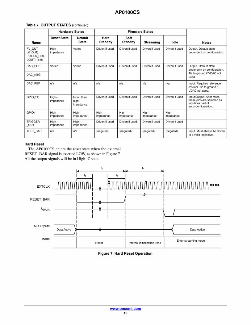
Hard ResetThe AP0100CS enters the reset state when the external
RESET_BAR signal is asserted LOW, as shown in Figure 7.All the output signals will be in High−Z state.
EXTCLK
RESET_BAR
All Outputs
Mode
Data Active Data Active
Reset Internal Initialization TimeEnter streaming mode
t1 t4
t2 t3
Figure 7. Hard Reset Operation
SDATA
AP0100CS
www.onsemi.com11
Table 8. HARD RESET
Symbol Parameter Min Typ Max Unit
t1 RESET_BAR pulse width 50 − − EXTCLK cycles
t2 Active EXTCLK required after RESET_BAR asserted 10 − −
t3 Active EXTCLK required before RESET_BAR de−asserted 10 − −
t4 First two−wire serial interface communication after RESET_BAR is HIGH
100 − −
Soft ResetA soft reset sequence to the AP0100CS can be activated
by writing to a register through the two−wire serial interface.
Hard Standby ModeThe AP0100CS can enter hard standby mode by using the
external STANDBY signal, as shown in Figure 8.
Entering Standby Mode1. Assert STANDBY signal HIGH.
Exiting Standby Mode1. De−assert STANDBY signal LOW.
EXTCLK
ModeSTANDBYAsserted
t1 t2 t3
STANDBY
STANDBYMode
EXTCLK Disabled EXTCLK Enabled
Figure 8. Hard Standby Operation
Table 9. HARD STANDBY SIGNAL TIMING
Symbol Parameter Min Typ Max Unit
t1 Standby entry complete − − 2 Frames Lines
t2 Active EXTCLK required after going into STANDBY mode 10 − − EXTCLKs
t3 Active EXTCLK required before STANDBY de−asserted 10 − − EXTCLKs
MULTI−CAMERA SYNCHRONIZATION SUPPORTThe AP0100CS supports multi−camera synchronization
through the FRAME_SYNC pin.The behavior will be different depending if the user is
using interlaced or progressive mode.When using the interlaced modes, on the rising edge of
FRAME_SYNC this will cause the output to stop the currentframe (A) and during B the image output will be
indeterminate. On the falling edge of FRAME_SYNC thiswill cause the re−synchronization to begin, this will continuefor a period (C), during C black fields will be output. There−synchronized interlaced signal will be available at D.During C if the user toggles the FRAME_SYNC input theAP0100CS will ignore it, the user cannot re−synchronizeagain until at D.
FRAME_SYNC
Figure 9. Frame Sync Behavior with Interlaced Mode
CVBS output(NTSC/PAL) A B C D
AP0100CS
www.onsemi.com12
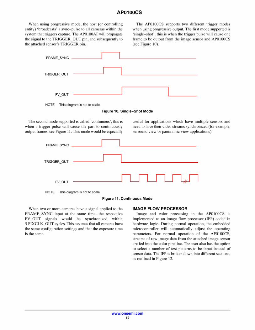
When using progressive mode, the host (or controllingentity) ‘broadcasts’ a sync−pulse to all cameras within thesystem that triggers capture. The AP0100AT will propagatethe signal to the TRIGGER_OUT pin, and subsequently tothe attached sensor’s TRIGGER pin.
The AP0100CS supports two different trigger modeswhen using progressive output. The first mode supported is‘single−shot’; this is when the trigger pulse will cause oneframe to be output from the image sensor and AP0100CS(see Figure 10).
FRAME_SYNC
Figure 10. Single−Shot Mode
TRIGGER_OUT
FV_OUT
NOTE: This diagram is not to scale.
The second mode supported is called ’continuous’, this iswhen a trigger pulse will cause the part to continuouslyoutput frames, see Figure 11. This mode would be especially
useful for applications which have multiple sensors andneed to have their video streams synchronized (for example,surround view or panoramic view applications).
FRAME_SYNC
Figure 11. Continuous Mode
TRIGGER_OUT
FV_OUT
NOTE: This diagram is not to scale.
When two or more cameras have a signal applied to theFRAME_SYNC input at the same time, the respectiveFV_OUT signals would be synchronized within5 PIXCLK_OUT cycles. This assumes that all cameras havethe same configuration settings and that the exposure timeis the same.
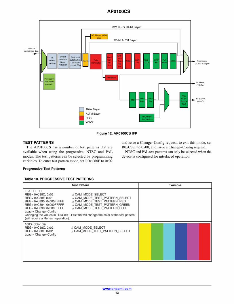
IMAGE FLOW PROCESSORImage and color processing in the AP0100CS is
implemented as an image flow processor (IFP) coded inhardware logic. During normal operation, the embeddedmicrocontroller will automatically adjust the operatingparameters. For normal operation of the AP0100CS,streams of raw image data from the attached image sensorare fed into the color pipeline. The user also has the optionto select a number of test patterns to be input instead ofsensor data. The IFP is broken down into different sections,as outlined in Figure 12.
AP0100CS
www.onsemi.com13
Figure 12. AP0100CS IFP
RAW 12− or 20−bit Bayer
12−bit ALTM Bayer
RAW Bayer
ALTM Bayer
RGB
YCbCr
RXdecom
panding
Black levelsubstractionDigital gain
control, PGA
Defectcorrection
Noisereduction
linear orcompanded data
ProgressiveTest patterngenerator
ALTM
AE, FD and ALTMstats
Colorinterpolation
ColorCor−rec−tion
Aper−tureCor−rec−tion
Crop Gam-ma
AW B stats
RGB−2YUV
ColorKill
YUVfilters
Scaler Progressive(YCbCr or Bayer)
Inter−lacer
Over−laySTE
PAL/NTSC
EncodeDAC
PAL/NTSCTest patterns
CCIR656(YCbCr)
NTSC/PAL(YCbCr)
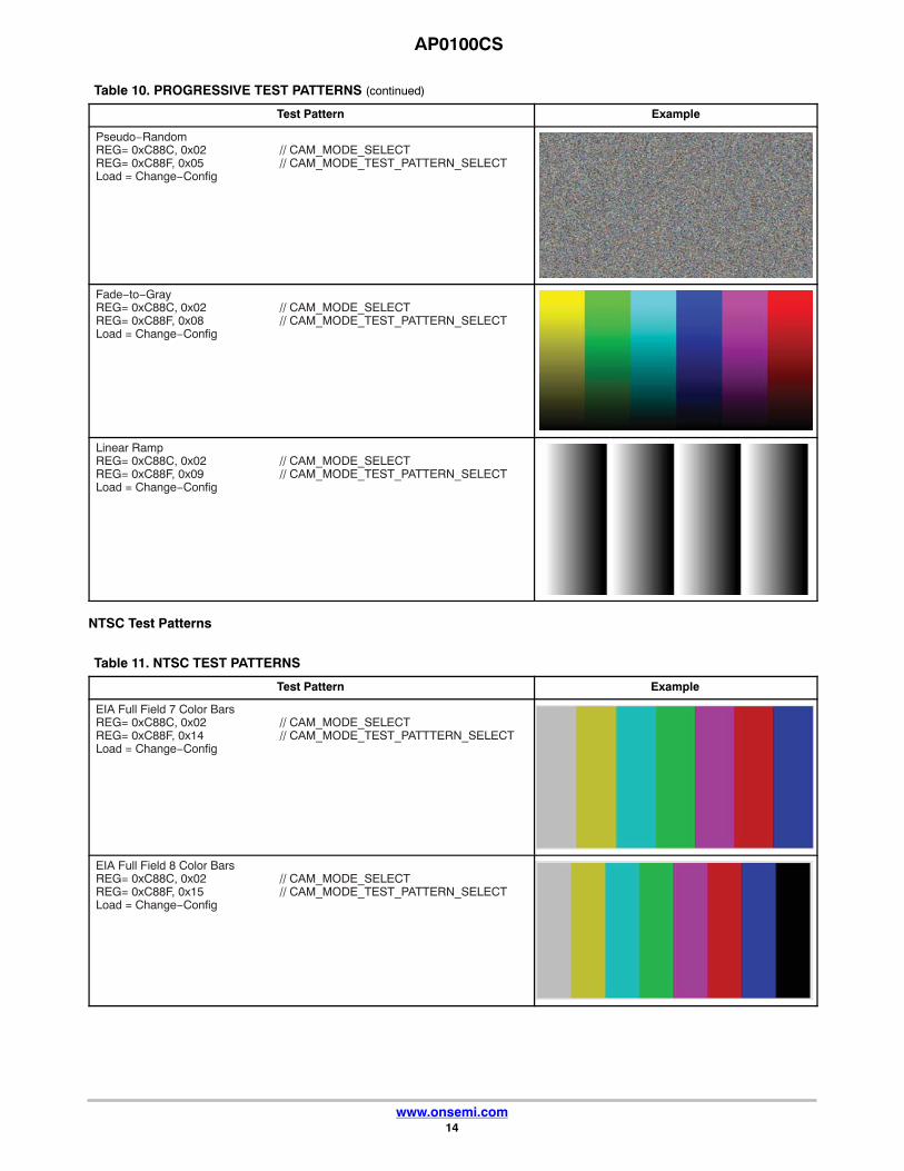
TEST PATTERNSThe AP0100CS has a number of test patterns that are
available when using the progressive, NTSC and PALmodes. The test patterns can be selected by programmingvariables. To enter test pattern mode, set R0xC88F to 0x02
and issue a Change−Config request; to exit this mode, setR0xC88F to 0x00, and issue a Change−Config request.
NTSC and PAL test patterns can only be selected when thedevice is configured for interlaced operation.
Progressive Test Patterns
Table 10. PROGRESSIVE TEST PATTERNS
Test Pattern Example
FLAT FIELDREG= 0xC88C, 0x02 // CAM_MODE_SELECTREG= 0xC88F, 0x01 // CAM_MODE_TEST_PATTERN_SELECTREG= 0xC890, 0x000FFFFF // CAM_MODE_TEST_PATTERN_REDREG= 0xC894, 0x000FFFFF // CAM_MODE_TEST_PATTERN_GREENREG= 0xC898, 0x000FFFFF // CAM_MODE_TEST_PATTERN_BLUELoad = Change−ConfigChanging the values in R0xC890−R0x898 will change the color of the test pattern(will require a Refresh operation).
100% Color BarREG= 0xC88C, 0x02 // CAM_MODE_SELECTREG= 0xC88F, 0x02 // CAM_MODE_TEST_PATTERN_SELECTLoad = Change−Config
AP0100CS
www.onsemi.com14
Table 10. PROGRESSIVE TEST PATTERNS (continued)
Test Pattern Example
Pseudo−RandomREG= 0xC88C, 0x02 // CAM_MODE_SELECTREG= 0xC88F, 0x05 // CAM_MODE_TEST_PATTERN_SELECTLoad = Change−Config
Fade−to−GrayREG= 0xC88C, 0x02 // CAM_MODE_SELECTREG= 0xC88F, 0x08 // CAM_MODE_TEST_PATTERN_SELECTLoad = Change−Config
Linear RampREG= 0xC88C, 0x02 // CAM_MODE_SELECTREG= 0xC88F, 0x09 // CAM_MODE_TEST_PATTERN_SELECTLoad = Change−Config
NTSC Test Patterns
Table 11. NTSC TEST PATTERNS
Test Pattern Example
EIA Full Field 7 Color BarsREG= 0xC88C, 0x02 // CAM_MODE_SELECTREG= 0xC88F, 0x14 // CAM_MODE_TEST_PATTTERN_SELECTLoad = Change−Config
EIA Full Field 8 Color BarsREG= 0xC88C, 0x02 // CAM_MODE_SELECTREG= 0xC88F, 0x15 // CAM_MODE_TEST_PATTERN_SELECTLoad = Change−Config
AP0100CS
www.onsemi.com15
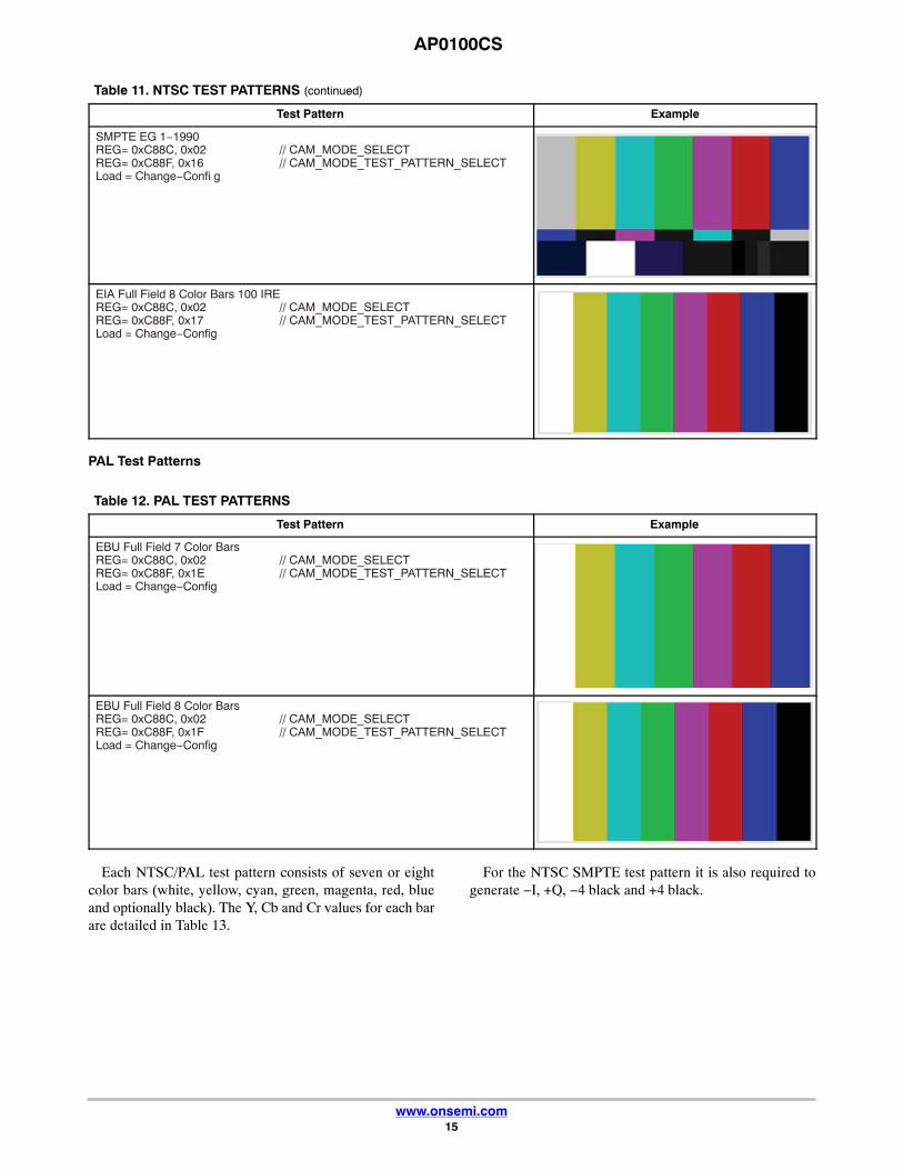
Table 11. NTSC TEST PATTERNS (continued)
Test Pattern Example
SMPTE EG 1−1990REG= 0xC88C, 0x02 // CAM_MODE_SELECTREG= 0xC88F, 0x16 // CAM_MODE_TEST_PATTERN_SELECTLoad = Change−Confi g
EIA Full Field 8 Color Bars 100 IREREG= 0xC88C, 0x02 // CAM_MODE_SELECTREG= 0xC88F, 0x17 // CAM_MODE_TEST_PATTERN_SELECTLoad = Change−Config
PAL Test Patterns
Table 12. PAL TEST PATTERNS
Test Pattern Example
EBU Full Field 7 Color BarsREG= 0xC88C, 0x02 // CAM_MODE_SELECTREG= 0xC88F, 0x1E // CAM_MODE_TEST_PATTERN_SELECTLoad = Change−Config
EBU Full Field 8 Color BarsREG= 0xC88C, 0x02 // CAM_MODE_SELECTREG= 0xC88F, 0x1F // CAM_MODE_TEST_PATTERN_SELECTLoad = Change−Config
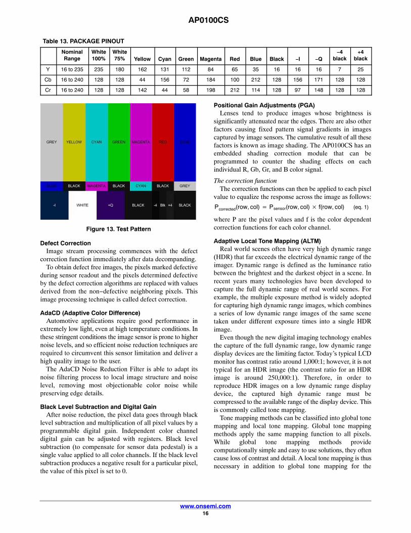
Each NTSC/PAL test pattern consists of seven or eightcolor bars (white, yellow, cyan, green, magenta, red, blueand optionally black). The Y, Cb and Cr values for each barare detailed in Table 13.
For the NTSC SMPTE test pattern it is also required togenerate −I, +Q, −4 black and +4 black.
AP0100CS
www.onsemi.com16
Table 13. PACKAGE PINOUT
NominalRange
White100%
White75% Yellow Cyan Green Magenta Red Blue Black −I −Q
−4black
+4black
Y 16 to 235 235 180 162 131 112 84 65 35 16 16 16 7 25
Cb 16 to 240 128 128 44 156 72 184 100 212 128 156 171 128 128
Cr 16 to 240 128 128 142 44 58 198 212 114 128 97 148 128 128
Figure 13. Test Pattern
Defect CorrectionImage stream processing commences with the defect
correction function immediately after data decompanding.To obtain defect free images, the pixels marked defective
during sensor readout and the pixels determined defectiveby the defect correction algorithms are replaced with valuesderived from the non−defective neighboring pixels. Thisimage processing technique is called defect correction.
AdaCD (Adaptive Color Difference)Automotive applications require good performance in
extremely low light, even at high temperature conditions. Inthese stringent conditions the image sensor is prone to highernoise levels, and so efficient noise reduction techniques arerequired to circumvent this sensor limitation and deliver ahigh quality image to the user.
The AdaCD Noise Reduction Filter is able to adapt itsnoise filtering process to local image structure and noiselevel, removing most objectionable color noise whilepreserving edge details.
Black Level Subtraction and Digital GainAfter noise reduction, the pixel data goes through black
level subtraction and multiplication of all pixel values by aprogrammable digital gain. Independent color channeldigital gain can be adjusted with registers. Black levelsubtraction (to compensate for sensor data pedestal) is asingle value applied to all color channels. If the black levelsubtraction produces a negative result for a particular pixel,the value of this pixel is set to 0.
Positional Gain Adjustments (PGA)Lenses tend to produce images whose brightness is
significantly attenuated near the edges. There are also otherfactors causing fixed pattern signal gradients in imagescaptured by image sensors. The cumulative result of all thesefactors is known as image shading. The AP0100CS has anembedded shading correction module that can beprogrammed to counter the shading effects on eachindividual R, Gb, Gr, and B color signal.
The correction functionThe correction functions can then be applied to each pixel
value to equalize the response across the image as follows:
Pcorrected(row, col) � Psensor(row, col) � f(row, col) (eq. 1)
where P are the pixel values and f is the color dependentcorrection functions for each color channel.
Adaptive Local Tone Mapping (ALTM)Real world scenes often have very high dynamic range
(HDR) that far exceeds the electrical dynamic range of theimager. Dynamic range is defined as the luminance ratiobetween the brightest and the darkest object in a scene. Inrecent years many technologies have been developed tocapture the full dynamic range of real world scenes. Forexample, the multiple exposure method is widely adoptedfor capturing high dynamic range images, which combinesa series of low dynamic range images of the same scenetaken under different exposure times into a single HDRimage.
Even though the new digital imaging technology enablesthe capture of the full dynamic range, low dynamic rangedisplay devices are the limiting factor. Today’s typical LCDmonitor has contrast ratio around 1,000:1; however, it is nottypical for an HDR image (the contrast ratio for an HDRimage is around 250,000:1). Therefore, in order toreproduce HDR images on a low dynamic range displaydevice, the captured high dynamic range must becompressed to the available range of the display device. Thisis commonly called tone mapping.
Tone mapping methods can be classified into global tonemapping and local tone mapping. Global tone mappingmethods apply the same mapping function to all pixels.While global tone mapping methods providecomputationally simple and easy to use solutions, they oftencause loss of contrast and detail. A local tone mapping is thusnecessary in addition to global tone mapping for the
AP0100CS
www.onsemi.com17
reproduction of visually more appealing images that alsoreveal scene details that are important for automotive safetyand surveillance applications. Local tone mapping methodsuse a spatially variable mapping function determined by theneighborhood of a pixel, which allows it to increase the localcontrast and the visibility of some details of the image. Localmethods usually yield more pleasing results because theyexploit the fact that human vision is more sensitive to localcontrast.
ON Semiconductor’s ALTM solution significantlyimproves the performance over global tone mapping.ALTM is directly applied to the Bayer domain to compressthe dynamic range from 20− bit to 12−bit. This allows theregular color pipeline to be used for HDR image rendering.
Color InterpolationIn the raw data stream fed by the external sensor to the IFP,
each pixel is represented by a 20− or 12−bit integer number,which can be considered proportional to the pixel’s responseto a one−color light stimulus, red, green, or blue, dependingon the pixel’s position under the color filter array. Initial dataprocessing steps, up to and including ALTM, preserve theone−color−per−pixel nature of the data stream, but afterALTM it must be converted to a three−colors−per−pixelstream appropriate for standard color processing. Theconversion is done by an edge−sensitive color interpolationmodule. The module pads the incomplete color informationavailable for each pixel with information extracted from anappropriate set of neighboring pixels. The algorithm used toselect this set and extract the information seeks the bestcompromise between preserving edges and filtering outhigh frequency noise in flat field areas. The edge thresholdcan be set through register settings.
Color correction and aperture correctionTo achieve good color fidelity of the IFP output,
interpolated RGB values of all pixels are subjected to colorcorrection. The IFP multiplies each vector of three pixelcolors by a 3 x 3 color correction matrix. The threecomponents of the resulting color vector are all sums of three10−bit numbers. The color correction matrix can be eitherprogrammed by the user or automatically selected by theauto white balance (AWB) algorithm implemented in theIFP. Color correction should ideally produce output colorsthat are corrected for the spectral sensitivity and colorcrosstalk characteristics of the image sensor. The optimalvalues of the color correction matrix elements depend onthose sensor characteristics and on the spectrum of lightincident on the sensor. The color correction variables can beadjusted through register settings.
Traditionally this would have been derived from two setsof CCM, one for Warm light like Tungsten and the other forDaylight (the part would interpolate between the twomatrices). This is not an optimal solution for cameras usedin a Cool White Fluorescent (CWF) environment. A better
solution is to provide three CCMs, which would include amatrix for CWF (interpolation now between three matrices).The AP0100CS offers this feature which will give the userimproved color fidelity when under CWF type lighting.
To increase image sharpness, a programmable 2Daperture correction (sharpening filter) is applied tocolor−corrected image data. The gain and threshold for 2Dcorrection can be defined through register settings.
Gamma CorrectionThe gamma correction curve is implemented as a
piecewise linear function with 33 knee points, taking 12−bitarguments and mapping them to 10−bit output. Theabscissas of the knee points are fixed at 0, 8, 16, 24, 32, 40,48, 56, 64, 80, 96, 112, 128, 160, 192, 224, 256, 320, 384,448, 512, 640, 768, 896, 1024, 1280, 1536, 1792, 2048,2560, 3072, 3584, and 4096. The 10−bit ordinates areprogrammable through variables.
The AP0100CS has the ability to calculate the 33−pointknee points based on the tuning of cam_ll_gamma andcam_ll_contrast_gradient_bright. The other method is forthe host to program the 33 knee point curve themselves.
Also included in this block is a Fade−to Black curve whichsets all knee points to zero and causes the image to go blackin extreme low light conditions.
Color killTo remove high−or low−light color artifacts, a color kill
circuit is included. It affects only pixels whose luminanceexceeds a certain preprogrammed threshold. The U and Vvalues of those pixels are attenuated proportionally to thedifference between their luminance and the threshold.
YUV color filterAs an optional processing step, noise suppression by
one−dimensional low−pass filtering of Y and/or UV signalsis possible. A 3− or 5−tap filter can be selected for eachsignal.
CAMERA CONTROL AND AUTO FUNCTIONS
Auto ExposureThe auto exposure algorithm optimizes scene exposure to
minimize clipping and saturation in critical areas of theimage. This is achieved by controlling exposure time andanalog gains of the external sensor as well as digital gainsapplied to the image.
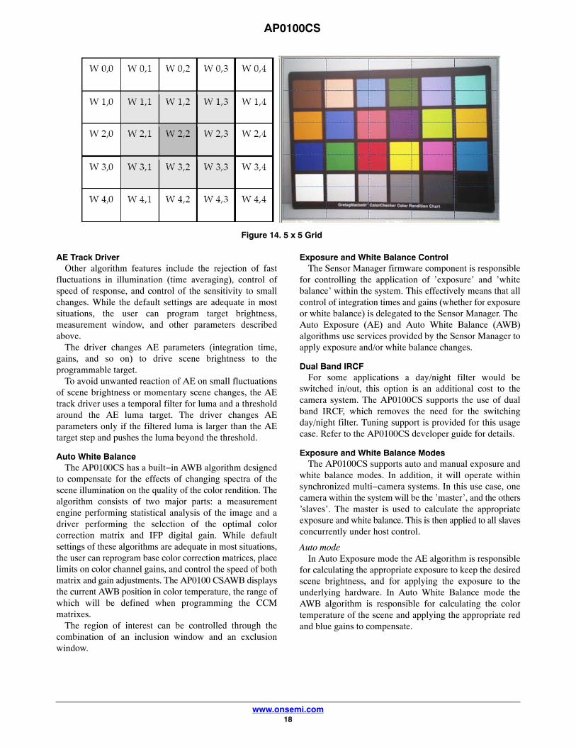
Auto exposure is implemented by a firmware algorithmthat is running on the embedded microcontroller thatanalyzes image statistics collected by the exposuremeasurement engine, makes a decision, and programs thesensor and color pipeline to achieve the desired exposure.The measurement engine subdivides the image into 25windows organized as a 5 x 5 grid
AP0100CS
www.onsemi.com18
Figure 14. 5 x 5 Grid
AE Track DriverOther algorithm features include the rejection of fast
fluctuations in illumination (time averaging), control ofspeed of response, and control of the sensitivity to smallchanges. While the default settings are adequate in mostsituations, the user can program target brightness,measurement window, and other parameters describedabove.
The driver changes AE parameters (integration time,gains, and so on) to drive scene brightness to theprogrammable target.
To avoid unwanted reaction of AE on small fluctuationsof scene brightness or momentary scene changes, the AEtrack driver uses a temporal filter for luma and a thresholdaround the AE luma target. The driver changes AEparameters only if the filtered luma is larger than the AEtarget step and pushes the luma beyond the threshold.
Auto White BalanceThe AP0100CS has a built−in AWB algorithm designed
to compensate for the effects of changing spectra of thescene illumination on the quality of the color rendition. Thealgorithm consists of two major parts: a measurementengine performing statistical analysis of the image and adriver performing the selection of the optimal colorcorrection matrix and IFP digital gain. While defaultsettings of these algorithms are adequate in most situations,the user can reprogram base color correction matrices, placelimits on color channel gains, and control the speed of bothmatrix and gain adjustments. The AP0100 CSAWB displaysthe current AWB position in color temperature, the range ofwhich will be defined when programming the CCMmatrixes.
The region of interest can be controlled through thecombination of an inclusion window and an exclusionwindow.
Exposure and White Balance ControlThe Sensor Manager firmware component is responsible
for controlling the application of ’exposure’ and ’whitebalance’ within the system. This effectively means that allcontrol of integration times and gains (whether for exposureor white balance) is delegated to the Sensor Manager. TheAuto Exposure (AE) and Auto White Balance (AWB)algorithms use services provided by the Sensor Manager toapply exposure and/or white balance changes.
Dual Band IRCFFor some applications a day/night filter would be
switched in/out, this option is an additional cost to thecamera system. The AP0100CS supports the use of dualband IRCF, which removes the need for the switchingday/night filter. Tuning support is provided for this usagecase. Refer to the AP0100CS developer guide for details.
Exposure and White Balance ModesThe AP0100CS supports auto and manual exposure and
white balance modes. In addition, it will operate withinsynchronized multi−camera systems. In this use case, onecamera within the system will be the ’master’, and the others’slaves’. The master is used to calculate the appropriateexposure and white balance. This is then applied to all slavesconcurrently under host control.
Auto modeIn Auto Exposure mode the AE algorithm is responsible
for calculating the appropriate exposure to keep the desiredscene brightness, and for applying the exposure to theunderlying hardware. In Auto White Balance mode theAWB algorithm is responsible for calculating the colortemperature of the scene and applying the appropriate redand blue gains to compensate.
AP0100CS
www.onsemi.com19
Triggered auto modeThe Triggered Auto Exposure and Triggered Auto White
Balance modes are intended for the multicamera use cases,where a host is controlling the exposure and white balanceof a number of cameras. The idea is that one camera is intriggered−auto mode (the master), and the others inhostcontrolled mode (slaves). The master camera mustcalculate the exposure and gains, the host then copies this tothe slaves, and all changes are then applied at the same time.
Manual modeManual mode is intended to allow simple manual
exposure and white balance control by the host. The hostneeds to set the CAM_AET_EXPOSURE_TIME_MS,CAM_AET_EXPOSURE_GAIN and CAM_AWB_COL−OR_TEMPERATURE controls, the camera will calculatethe appropriate integration times and gains.
Host controlledThe Host Controlled mode is intended to give the host full
control over exposure and gains.
FLICKER AVOIDANCEFlicker occurs when the integration time is not an integer
multiple of the period of the light intensity. The AP0100CScan be programmed to avoid flicker for 50 or 60 Hertz. Forintegration times below the light intensity period (10 ms for
50Hz environment), flicker cannot be avoided. TheAP0100CS supports an indoor AE mode, that will ensureflicker−free operation.
FLICKER DETECTIONThe AP0100CS supports flicker detection, the algorithm
is designed only to detect a 50 Hz or 60 Hz flicker source.
OUTPUT FORMATTINGThe pixel output data in AP0100CS will be transmitted as
an 8/10 bit word over one or two clocks.
Uncompressed YCbCr Data OrderingThe AP0100CS supports swapping YCbCr mode, as
illustrated in Table 14.
Table 14. YCbCr OUTPUT DATA ORDERING
Mode Data Sequence
Default (no swap) Cbi Yi Cri Yi+1
Swapped CrCb Cri Yi Cbi Yi+1
Swapped YC Yi Cbi Yi+1 Cri
Swapped CrCb, YC Yi Cri Yi+1 Cbi
The data ordering for the YCbCr output modes forAP0100CS are shown in Table 15:
Table 15. YCbCr Output Modes (cam_port_parallel_msb_align=0x1)
Mode Byte Pixel i Pixel i+1 Notes
YCbCr_422_8_8 Odd (DOUT [15:8]) Cbi Cri Data range of 0−255 (Y = 16−235 and C = 16−240)
Even (DOUT [15:8]) Yi Yi+1
YCbCr_422_10_10 Odd (DOUT [15:6]) Cbi Cri Data range of 0−1023 (Y = 64−940 and C = 64−960)
Even (DOUT [15:6]) Yi Yi+1
YCbCr_422_16 Single (DOUT [15:0]) Cbi_Yi Cri_Yi+1 Data range of 0−255 (Y = 16−235 and C = 16−240)
3. Odd means first cycle; even means second cycle.
Table 16. YCbCr Output Modes (cam_port_parallel_msb_align=0x0), cam_port_parallel_swap_bytes = 0,cam_output_format_yuv_swap_red_blue = 0)
Mode Byte Pixel i Pixel i+1 Notes
YCbCr_422_8_8 Odd (DOUT [7:0]) Cbi Cri Data range of 0−255 (Y = 16−235 and C = 16−240)
Even (DOUT [7:0]) Yi Yi+1
YCbCr_422_10_10 Odd (DOUT [9:0]) Cbi Cri Data range of 0−1023 (Y = 64−940 and C = 64−960)
Even (DOUT [9:0]) Yi Yi+1
YCbCr_422_16 Single (DOUT [15:0]) Cbi_Yi Cri_Yi+1 Data range of 0−255 (Y = 16−235 and C = 16−240)
AP0100CS
www.onsemi.com20
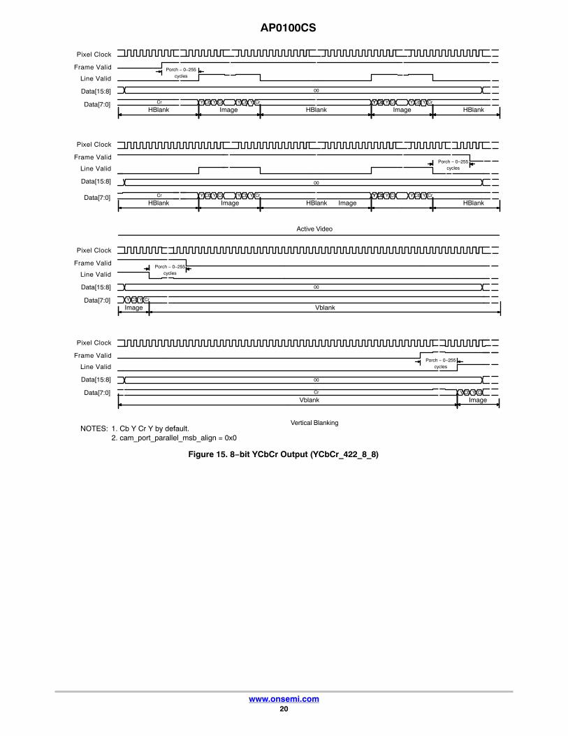
Figure 15. 8−bit YCbCr Output (YCbCr_422_8_8)
Line Valid
Frame Valid
Pixel Clock
Data[15:8]
Data[7:0]
Line Valid
Frame Valid
Pixel Clock
Data[15:8]
Line Valid
Frame Valid
Pixel Clock
Data[15:8]
Data[7:0]
Line Valid
Frame Valid
Pixel Clock
Data[15:8]
Data[7:0]
Porch − 0−255cycles
HBlankCr
ImageY Cb CrY Y Cb CrY
00
HBlankY CrY Cb CrCbY Cb YY
Image HBlank
Data[7:0]HBlank
Cr
ImageY Cb CrY Y Cb CrY
HBlankY CrY Cb CrCbY Cb YY
Image HBlank
00
Porch − 0−255cycles
Active Video
Porch − 0−255cycles
00
Y Cb CrY
Image Vblank
Porch − 0−255cycles
ImageVblank
00
Cr Y Cb CrY
Vertical BlankingNOTES: 1. Cb Y Cr Y by default.
2. cam_port_parallel_msb_align = 0x0
AP0100CS
www.onsemi.com21
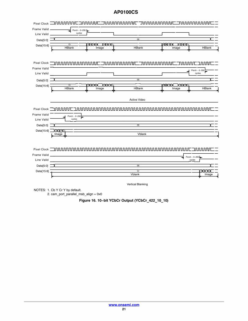
Figure 16. 10−bit YCbCr Output (YCbCr_422_10_10)
Line Valid
Frame Valid
Pixel Clock
Line Valid
Frame Valid
Pixel Clock
Line Valid
Frame Valid
Pixel Clock
Line Valid
Frame Valid
Pixel Clock
Porch − 0−255cycles
HBlankCr
ImageY Cb CrY Y Cb CrY
00
HBlankY CrY Cb CrCbY Cb YY
Image HBlank
HBlankCr
ImageY Cb CrY Y Cb CrY
HBlankY CrY Cb CrCbY Cb YY
Image HBlank
00
Porch − 0−255cycles
Active Video
Porch − 0−255cycles
00
Y Cb CrY
Image Vblank
Porch − 0−255cycles
ImageVblank
00
Cr Y Cb CrY
Vertical Blanking
Data[5:0]
Data[15:6]
Data[5:0]
Data[15:6]
Data[5:0]
Data[15:6]
Data[5:0]
Data[15:6]
NOTES: 1. Cb Y Cr Y by default.2. cam_port_parallel_msb_align = 0x0
AP0100CS
www.onsemi.com22
Figure 17. 16−bit YCbCr Output (YCbCr_422_16)
Line Valid
Frame Valid
Pixel Clock
Line Valid
Frame Valid
Pixel Clock
Line Valid
Frame Valid
Pixel Clock
Line Valid
Frame Valid
Pixel Clock
Porch − 0−255cycles
HBlankCr
ImageY Cb CrY Y Cb CrY
HBlankY CrY Cb CrCbY Cb YY
Image HBlank
HBlankCr
ImageY Cb CrY Y Cb CrY
HBlankY CrY Cb CrCbY Cb YY
Image HBlank
Porch − 0−255cycles
Active Video
Porch − 0−255cycles
Cr Cr
Image Vblank
Porch − 0−255cycles
ImageVblank
Y
Cr Cb
Vertical Blanking
Data[7:0]
Data[15:8]
Data[7:0]
Data[15:8]
Data[7:0]
Data[15:8]
Data[7:0]
Data[15:8]
Y Y Y YY Y Y YY YY Y Y Y Y Y Y Y
Y Y Y YY Y Y YY YY Y Y Y Y Y Y Y
Y Y YY
Cr Cr
Cb CbCb
Y Y YY
AP0100CS
www.onsemi.com23
Figure 18. Typical CCIR656 Output
Line Valid
Frame Valid
Pixel Clock
Data[7:0]
Data[15:8]
80 10 80 10 80 10 80 10 FF 00 00 80 Cb CrY Y Cb Y YCr FF 00 00 9D 80 80 1010 80 10 80 10 FF 00 00 80 Cb Y Cr Y Cb CrY Y FF 00 00 9D 80 10 80 10
HBlank
Blanking SAV Image EAV Blanking SAV Image EAV Blanking
HBlank HBlank
80 10 80 10 80 10 80 10 FF 00 00 80 Cb CrY Y Cb Y YCr FF 00 00 9D 80 80 1010 80 10 80 10 FF 00 00 80 Cb Y Cr Y Cb CrY Y FF 00 00 9D 80 10 80 10
HBlank
Blanking SAV Image EAV blank Blanking SAV blank Vblank EAV blank Blanking
HBlank HBlank
Line Valid
Frame Valid
Pixel Clock
Data[7:0]
Data[15:8]
Field 1
00
00
Line Valid
Frame Valid
Pixel Clock
Data[7:0]
Data[15:8]
80 10 80 10 80 10 80 10 FF 00 00 80 Cb CrY Y Cb Y YCr FF 00 00 9D 80 80 1010 80 10 80 10 FF 00 00 80 Cb Y Cr Y Cb CrY Y FF 00 00 9D 80 10 80 10
HBlank
Blanking SAV Image EAV Blanking SAV Image EAV Blanking
HBlank HBlank
80 10 80 10 80 10 80 10 FF 00 00 80 Cb CrY Y Cb Y YCr FF 00 00 9D 80 80 1010 80 10 80 10 FF 00 00 80 Cb Y Cr Y Cb CrY Y FF 00 00 9D 80 10 80 10
HBlank
Blanking SAV Image EAV blank Blanking SAV blank VBlank EAV blank Blanking
HBlank HBlank
Line Valid
Frame Valid
Pixel Clock
Data[7:0]
Data[15:8]
00
00
Field 2
Figure 19. Typical CVBS Output (NTSC/PAL)
Pre−EqualisationPulses
Post−EqualisingPulses
Serration Pulses
1 2 3 4 5 6 7 8 9
1 2 3 4 5 6 7 8 9
Line Valid to First Field Latency ~= STE Latency + 1 Field
Frame Valid In
Line Valid In
Video
Frame Valid In
Line Valid In
VideoPre−Equalisation
PulsesPost−Equalising
PulsesSerration Pulses
Field 1/3
Field 2/4
AP0100CS
www.onsemi.com24
BAYER MODESBayer output modes are only available in progressive
output mode before STE. The data ordering for the ALTMBayer output modes for AP0100CS are shown in Table 17.
Table 17. ALTM BAYER OUTPUT MODES
Mode Byte D15 D14 D13 D12 D11 D10 D9 D8 D7 D6 D5 D4 D3 D2 D1 D0
ALTM_Bayer_10 Single 0 0 0 0 0 0 D9 D8 D7 D6 D5 D4 D3 D2 D1 D0
ALTM_Bayer_12 Single 0 0 0 0 D11 D10 D9 D8 D7 D6 D5 D4 D3 D2 D1 D0
Table 17 and Table 18 show LSB aligned data; it ispossible by using register setting to obtain MSB aligneddata.
The data ordering for the Bayer output modes forAP0100CS are shown in Table 18.
Table 18. BAYER OUTPUT MODES
Mode Byte D15 D14 D13 D12 D11 D10 D9 D8 D7 D6 D5 D4 D3 D2 D1 D0 Notes
Bayer_12 Single 0 0 0 0 D11 D10 D9 D8 D7 D6 D5 D4 D3 D2 D1 D0 RAWBayerdata
4. Bayer_12 can be selected by setting cam_mode_select = 0x1 and requesting a Change−Config operation.
Sensor Embedded DataThe AP0100CS is capable of passing sensor embedded
data in Bayer output mode only.The AP0100CS Statistics are available through the serial
interface. Refer to the developer guide for details.
SPATIAL TRANSFORM ENGINE (STE)A spatial transform is defined as a transform in which
some pixels are in different positions within the input andoutput pictures. Examples include zoom, lens distortioncorrection, turn, and rotate. STE is a fully programmableengine which can perform spatial transforms and eliminatesthe need for an expensive DSP for image correction.
Lens Distortion CorrectionAutomotive backup cameras typically feature a wide
FOV lens so that a single camera mounted above the centerof the rear bumper can present the driver with a view of all
potential obstacles immediately behind the full width of thevehicle. Lenses with a wide field of view typically exhibit atleast a noticeable amount of barrel distortion.
Barrel distortion is caused by a reduction in objectmagnification the further away from the optical axis.
For the image to appear natural to the driver, theAP0100CS corrects this barrel distortion and reprocessesthe image so that the resulting distortion is much smaller.This is called distortion correction. Distortion correction isthe ability to digitally correct the lens barrel distortion andto provide a natural view of objects. In addition, with barreldistortion one can adjust the perspective view to enhance thevisibility by virtually elevating the point of viewing objects.
Pan, Tilt, Zoom and RotateUsing the STE it is possible to implement image
transformations like Pan, Tilt, Zoom and Rotate.
Figure 20. Uncorrected Image
AP0100CS
www.onsemi.com25
Figure 21. Zoomed
Figure 22. Zoom and Look Left
Figure 23. Zoom and Look Right
AP0100CS
www.onsemi.com26
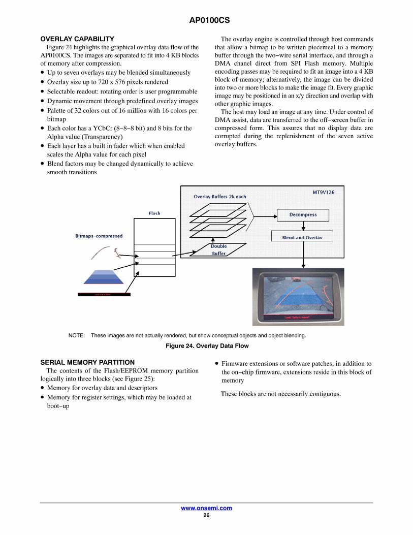
OVERLAY CAPABILITYFigure 24 highlights the graphical overlay data flow of the
AP0100CS. The images are separated to fit into 4 KB blocksof memory after compression.• Up to seven overlays may be blended simultaneously
• Overlay size up to 720 x 576 pixels rendered
• Selectable readout: rotating order is user programmable
• Dynamic movement through predefined overlay images
• Palette of 32 colors out of 16 million with 16 colors perbitmap
• Each color has a YCbCr (8−8−8 bit) and 8 bits for theAlpha value (Transparency)
• Each layer has a built in fader which when enabledscales the Alpha value for each pixel
• Blend factors may be changed dynamically to achievesmooth transitions
The overlay engine is controlled through host commandsthat allow a bitmap to be written piecemeal to a memorybuffer through the two−wire serial interface, and through aDMA chanel direct from SPI Flash memory. Multipleencoding passes may be required to fit an image into a 4 KBblock of memory; alternatively, the image can be dividedinto two or more blocks to make the image fit. Every graphicimage may be positioned in an x/y direction and overlap withother graphic images.
The host may load an image at any time. Under control ofDMA assist, data are transferred to the off−screen buffer incompressed form. This assures that no display data arecorrupted during the replenishment of the seven activeoverlay buffers.
Figure 24. Overlay Data Flow
NOTE: These images are not actually rendered, but show conceptual objects and object blending.
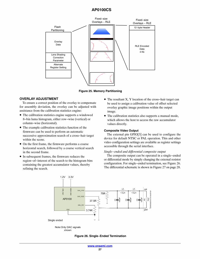
SERIAL MEMORY PARTITIONThe contents of the Flash/EEPROM memory partition
logically into three blocks (see Figure 25):• Memory for overlay data and descriptors
• Memory for register settings, which may be loaded atboot−up
• Firmware extensions or software patches; in addition tothe on−chip firmware, extensions reside in this block ofmemory
These blocks are not necessarily contiguous.
AP0100CS
www.onsemi.com27
Figure 25. Memory Partitioning
Fixed−sizeOverlays − RLE
FlashPartitioning
Fixed−sizeOverlays − RLE
OverlayData
Lens ShadingCorrectionParameter
AlternateRegister Setting
12−byte Header
RLE EncodedData4 Kb
OVERLAY ADJUSTMENTTo ensure a correct position of the overlay to compensate
for assembly deviation, the overlay can be adjusted withassistance from the calibration statistics engine:• The calibration statistics engine supports a windowed
8−bin luma histogram, either row−wise (vertical) orcolumn−wise (horizontal).
• The example calibration statistics function of thefirmware can be used to perform an automaticsuccessive approximation search of a cross−hair targetwithin the scene.
• On the first frame, the firmware performs a coarsehorizontal search, followed by a coarse vertical searchin the second frame.
• In subsequent frames, the firmware reduces theregion−of−interest of the search to the histogram binscontaining the greatest accumulator values, therebyrefining the search.
• The resultant X, Y location of the cross−hair target canbe used to assign a calibration value of offset selectedoverlay graphic image positions within the outputimage.
• The calibration statistics also supports a manual mode,which allows the host to access the raw accumulatorvalues directly.
Composite Video OutputThe external pin GPIO[3] can be used to configure the
device for default NTSC or PAL operation. This and othervideo configuration settings are available as register settingsaccessible through the serial interface.
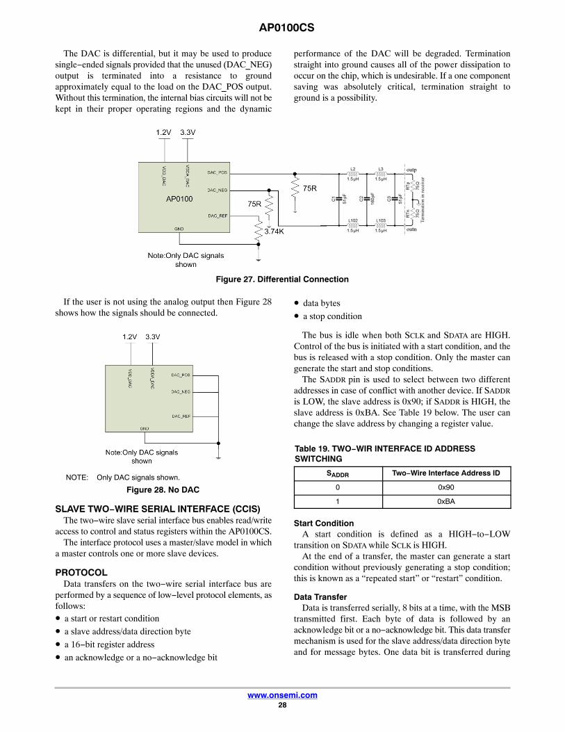
Single−ended and differential composite outputThe composite output can be operated in a single−ended
or differential mode by simply changing the external resistorconfiguration. For single−ended termination, see Figure 26.The differential schematic is shown in Figure 27 on page 28.
Figure 26. Single−Ended Termination
AP0100CS
www.onsemi.com28
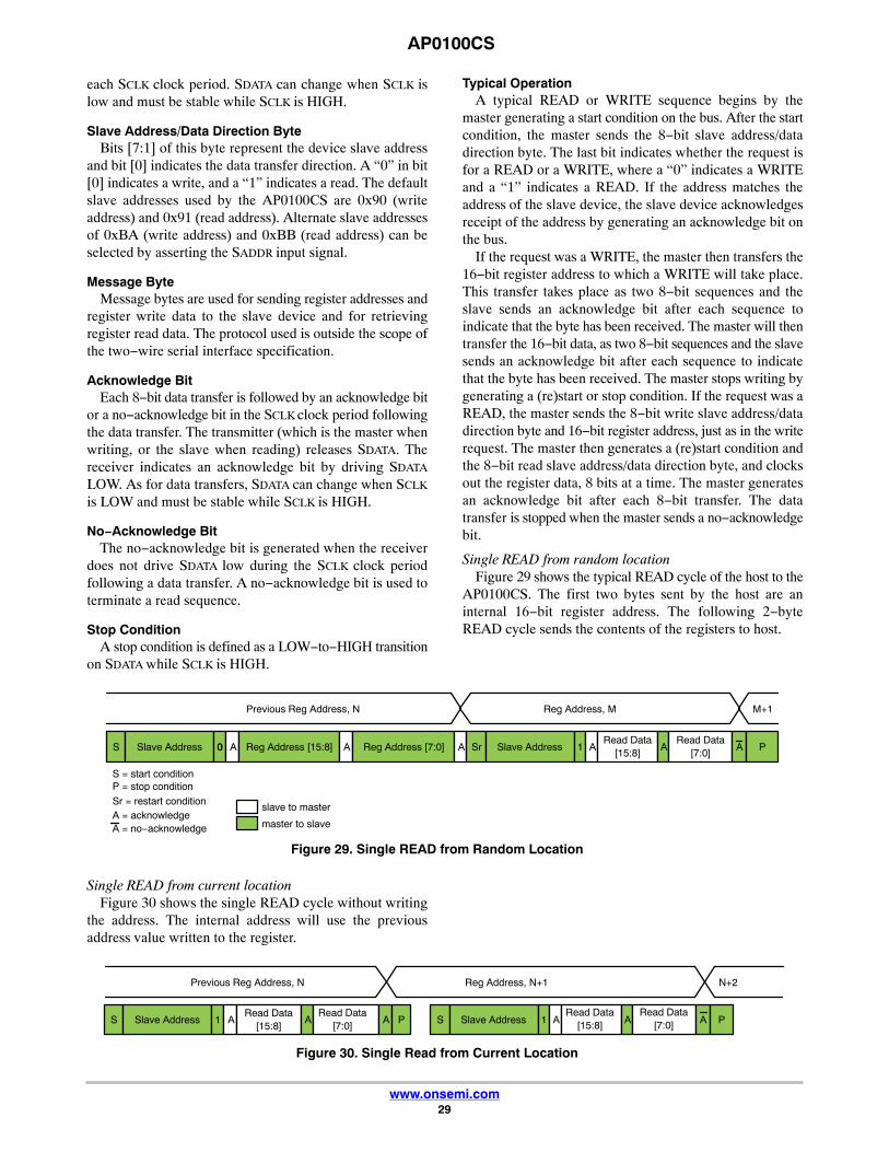
The DAC is differential, but it may be used to producesingle−ended signals provided that the unused (DAC_NEG)output is terminated into a resistance to groundapproximately equal to the load on the DAC_POS output.Without this termination, the internal bias circuits will not bekept in their proper operating regions and the dynamic
performance of the DAC will be degraded. Terminationstraight into ground causes all of the power dissipation tooccur on the chip, which is undesirable. If a one componentsaving was absolutely critical, termination straight toground is a possibility.
Figure 27. Differential Connection
If the user is not using the analog output then Figure 28shows how the signals should be connected.
Figure 28. No DAC
NOTE: Only DAC signals shown.
SLAVE TWO−WIRE SERIAL INTERFACE (CCIS)The two−wire slave serial interface bus enables read/write
access to control and status registers within the AP0100CS.The interface protocol uses a master/slave model in which
a master controls one or more slave devices.
PROTOCOLData transfers on the two−wire serial interface bus are
performed by a sequence of low−level protocol elements, asfollows:• a start or restart condition
• a slave address/data direction byte
• a 16−bit register address
• an acknowledge or a no−acknowledge bit
• data bytes
• a stop condition
The bus is idle when both SCLK and SDATA are HIGH.Control of the bus is initiated with a start condition, and thebus is released with a stop condition. Only the master cangenerate the start and stop conditions.
The SADDR pin is used to select between two differentaddresses in case of conflict with another device. If SADDR
is LOW, the slave address is 0x90; if SADDR is HIGH, theslave address is 0xBA. See Table 19 below. The user canchange the slave address by changing a register value.
Table 19. TWO−WIR INTERFACE ID ADDRESSSWITCHING
SADDR Two−Wire Interface Address ID
0 0x90
1 0xBA
Start ConditionA start condition is defined as a HIGH−to−LOW
transition on SDATA while SCLK is HIGH.At the end of a transfer, the master can generate a start
condition without previously generating a stop condition;this is known as a “repeated start” or “restart” condition.
Data TransferData is transferred serially, 8 bits at a time, with the MSB
transmitted first. Each byte of data is followed by anacknowledge bit or a no−acknowledge bit. This data transfermechanism is used for the slave address/data direction byteand for message bytes. One data bit is transferred during
AP0100CS
www.onsemi.com29
each SCLK clock period. SDATA can change when SCLK islow and must be stable while SCLK is HIGH.
Slave Address/Data Direction ByteBits [7:1] of this byte represent the device slave address
and bit [0] indicates the data transfer direction. A “0” in bit[0] indicates a write, and a “1” indicates a read. The defaultslave addresses used by the AP0100CS are 0x90 (writeaddress) and 0x91 (read address). Alternate slave addressesof 0xBA (write address) and 0xBB (read address) can beselected by asserting the SADDR input signal.
Message ByteMessage bytes are used for sending register addresses and
register write data to the slave device and for retrievingregister read data. The protocol used is outside the scope ofthe two−wire serial interface specification.
Acknowledge BitEach 8−bit data transfer is followed by an acknowledge bit
or a no−acknowledge bit in the SCLK clock period followingthe data transfer. The transmitter (which is the master whenwriting, or the slave when reading) releases SDATA. Thereceiver indicates an acknowledge bit by driving SDATA
LOW. As for data transfers, SDATA can change when SCLK
is LOW and must be stable while SCLK is HIGH.
No−Acknowledge BitThe no−acknowledge bit is generated when the receiver
does not drive SDATA low during the SCLK clock periodfollowing a data transfer. A no−acknowledge bit is used toterminate a read sequence.
Stop ConditionA stop condition is defined as a LOW−to−HIGH transition
on SDATA while SCLK is HIGH.
Typical OperationA typical READ or WRITE sequence begins by the
master generating a start condition on the bus. After the startcondition, the master sends the 8−bit slave address/datadirection byte. The last bit indicates whether the request isfor a READ or a WRITE, where a “0” indicates a WRITEand a “1” indicates a READ. If the address matches theaddress of the slave device, the slave device acknowledgesreceipt of the address by generating an acknowledge bit onthe bus.
If the request was a WRITE, the master then transfers the16−bit register address to which a WRITE will take place.This transfer takes place as two 8−bit sequences and theslave sends an acknowledge bit after each sequence toindicate that the byte has been received. The master will thentransfer the 16−bit data, as two 8−bit sequences and the slavesends an acknowledge bit after each sequence to indicatethat the byte has been received. The master stops writing bygenerating a (re)start or stop condition. If the request was aREAD, the master sends the 8−bit write slave address/datadirection byte and 16−bit register address, just as in the writerequest. The master then generates a (re)start condition andthe 8−bit read slave address/data direction byte, and clocksout the register data, 8 bits at a time. The master generatesan acknowledge bit after each 8−bit transfer. The datatransfer is stopped when the master sends a no−acknowledgebit.
Single READ from random locationFigure 29 shows the typical READ cycle of the host to the
AP0100CS. The first two bytes sent by the host are aninternal 16−bit register address. The following 2−byteREAD cycle sends the contents of the registers to host.
Figure 29. Single READ from Random Location
Previous Reg Address, N Reg Address, M M+1
S Slave Address 00 A Reg Address [15:8] Reg Address [7:0] Slave AddressA A A A ASr 1Read Data
[15:8]Read Data
[7:0]P
S = start conditionP = stop conditionSr = restart conditionA = acknowledgeA = no−acknowledge
slave to master
master to slave
Single READ from current locationFigure 30 shows the single READ cycle without writing
the address. The internal address will use the previousaddress value written to the register.
Figure 30. Single Read from Current Location
Previous Reg Address, N Reg Address, N+1 N+2
S Slave Address 1 A Slave AddressA A A A AS 1Read Data
[15:8]Read Data
[7:0]PP
Read Data[15:8]
Read Data[7:0]
AP0100CS
www.onsemi.com30
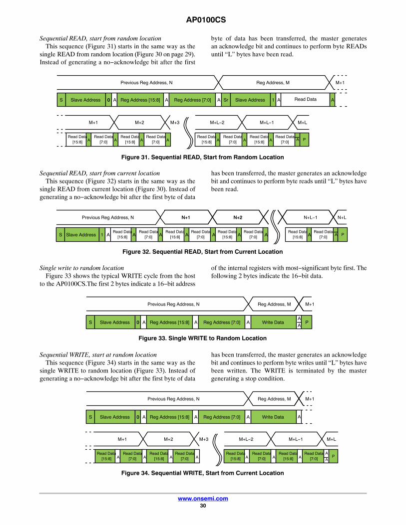
Sequential READ, start from random locationThis sequence (Figure 31) starts in the same way as the
single READ from random location (Figure 30 on page 29).Instead of generating a no−acknowledge bit after the first
byte of data has been transferred, the master generatesan acknowledge bit and continues to perform byte READsuntil “L” bytes have been read.
Figure 31. Sequential READ, Start from Random Location
Previous Reg Address, N Reg Address, M M+1
S Slave Address 00 A Reg Address [15:8] Reg Address [7:0] Slave AddressA A A ASr 1 Read Data
M+1 M+2 M+3 M+L−2 M+LM+L−1
Read Data[15:8]
Read Data[7:0]
Read Data[15:8]A
Read Data[7:0]
Read Data[7:0]
Read Data[15:8]
Read Data[7:0]
Read Data[15:8]
A PA A A A A A
Sequential READ, start from current locationThis sequence (Figure 32) starts in the same way as the
single READ from current location (Figure 30). Instead ofgenerating a no−acknowledge bit after the first byte of data
has been transferred, the master generates an acknowledgebit and continues to perform byte reads until “L” bytes havebeen read.
Figure 32. Sequential READ, Start from Current Location
Previous Reg Address, N
S Slave Address 1 ARead Data
[15:8]Read Data
[7:0]Read Data
[15:8]Read Data
[7:0]Read Data
[15:8]Read Data
[7:0]A P
N+1 N+2
Read Data[7:0]
Read Data[15:8]
N+1 N+2 N+L−1 N+L
A A A A A A A
Single write to random locationFigure 33 shows the typical WRITE cycle from the host
to the AP0100CS.The first 2 bytes indicate a 16−bit address
of the internal registers with most−significant byte first. Thefollowing 2 bytes indicate the 16−bit data.
Figure 33. Single WRITE to Random Location
Previous Reg Address, N M+1
S Slave Address 00 A Reg Address [15:8] Reg Address [7:0] Write DataA AA
PA
Reg Address, M
Sequential WRITE, start at random locationThis sequence (Figure 34) starts in the same way as the
single WRITE to random location (Figure 33). Instead ofgenerating a no−acknowledge bit after the first byte of data
has been transferred, the master generates an acknowledgebit and continues to perform byte writes until “L” bytes havebeen written. The WRITE is terminated by the mastergenerating a stop condition.
Figure 34. Sequential WRITE, Start from Current Location
Previous Reg Address, N M+1
S Slave Address 00 A Reg Address [15:8] Reg Address [7:0] Write DataA A A
Reg Address, M
M+1 M+2 M+3 M+L−2 M+LM+L−1
Read Data[15:8]
Read Data[7:0]
Read Data[15:8]A
Read Data[7:0]
Read Data[7:0]
Read Data[15:8]
Read Data[7:0]
Read Data[15:8] A
PA A A A A AA
AP0100CS
www.onsemi.com31
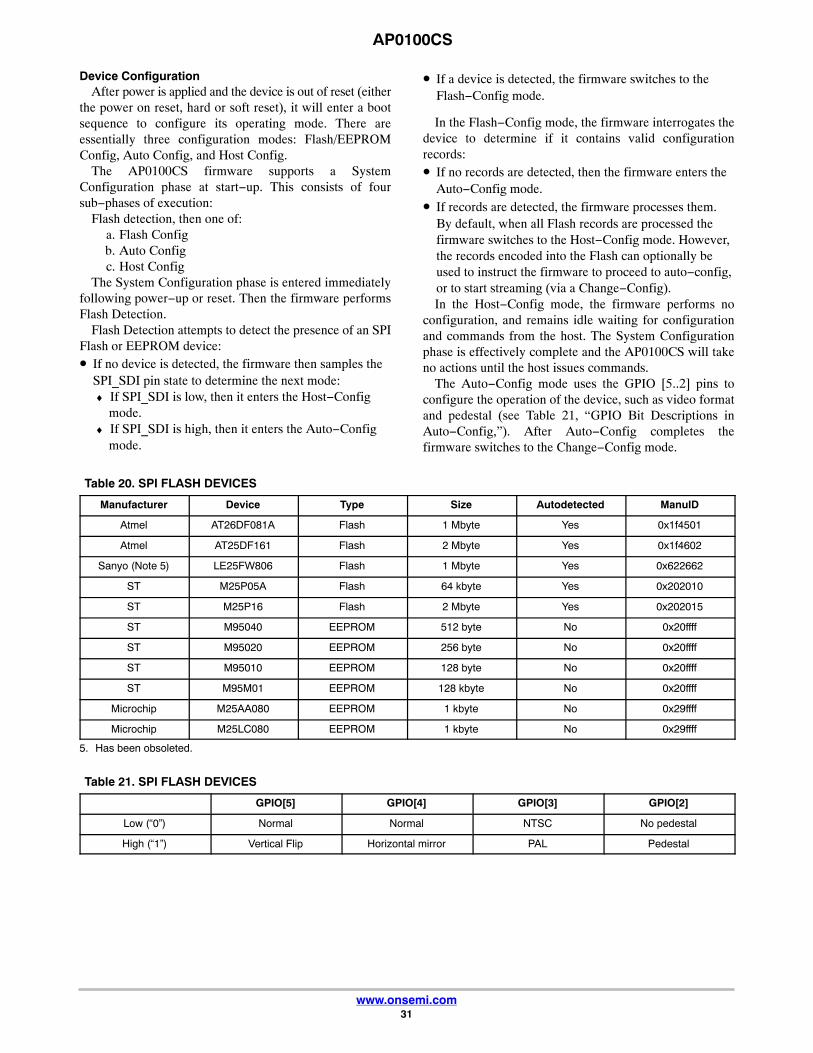
Device ConfigurationAfter power is applied and the device is out of reset (either
the power on reset, hard or soft reset), it will enter a bootsequence to configure its operating mode. There areessentially three configuration modes: Flash/EEPROMConfig, Auto Config, and Host Config.
The AP0100CS firmware supports a SystemConfiguration phase at start−up. This consists of foursub−phases of execution:
Flash detection, then one of:a. Flash Configb. Auto Configc. Host Config
The System Configuration phase is entered immediatelyfollowing power−up or reset. Then the firmware performsFlash Detection.
Flash Detection attempts to detect the presence of an SPIFlash or EEPROM device:• If no device is detected, the firmware then samples the
SPI_SDI pin state to determine the next mode:♦ If SPI_SDI is low, then it enters the Host−Config
mode.♦ If SPI_SDI is high, then it enters the Auto−Config
mode.
• If a device is detected, the firmware switches to theFlash−Config mode.
In the Flash−Config mode, the firmware interrogates thedevice to determine if it contains valid configurationrecords:• If no records are detected, then the firmware enters the
Auto−Config mode.• If records are detected, the firmware processes them.
By default, when all Flash records are processed thefirmware switches to the Host−Config mode. However,the records encoded into the Flash can optionally beused to instruct the firmware to proceed to auto−config,or to start streaming (via a Change−Config).In the Host−Config mode, the firmware performs no
configuration, and remains idle waiting for configurationand commands from the host. The System Configurationphase is effectively complete and the AP0100CS will takeno actions until the host issues commands.
The Auto−Config mode uses the GPIO [5..2] pins toconfigure the operation of the device, such as video formatand pedestal (see Table 21, “GPIO Bit Descriptions inAuto−Config,”). After Auto−Config completes thefirmware switches to the Change−Config mode.
Table 20. SPI FLASH DEVICES
Manufacturer Device Type Size Autodetected ManuID
Atmel AT26DF081A Flash 1 Mbyte Yes 0x1f4501
Atmel AT25DF161 Flash 2 Mbyte Yes 0x1f4602
Sanyo (Note 5) LE25FW806 Flash 1 Mbyte Yes 0x622662
ST M25P05A Flash 64 kbyte Yes 0x202010
ST M25P16 Flash 2 Mbyte Yes 0x202015
ST M95040 EEPROM 512 byte No 0x20ffff
ST M95020 EEPROM 256 byte No 0x20ffff
ST M95010 EEPROM 128 byte No 0x20ffff
ST M95M01 EEPROM 128 kbyte No 0x20ffff
Microchip M25AA080 EEPROM 1 kbyte No 0x29ffff
Microchip M25LC080 EEPROM 1 kbyte No 0x29ffff
5. Has been obsoleted.
Table 21. SPI FLASH DEVICES
GPIO[5] GPIO[4] GPIO[3] GPIO[2]
Low (“0”) Normal Normal NTSC No pedestal
High (“1”) Vertical Flip Horizontal mirror PAL Pedestal
AP0100CS
www.onsemi.com32
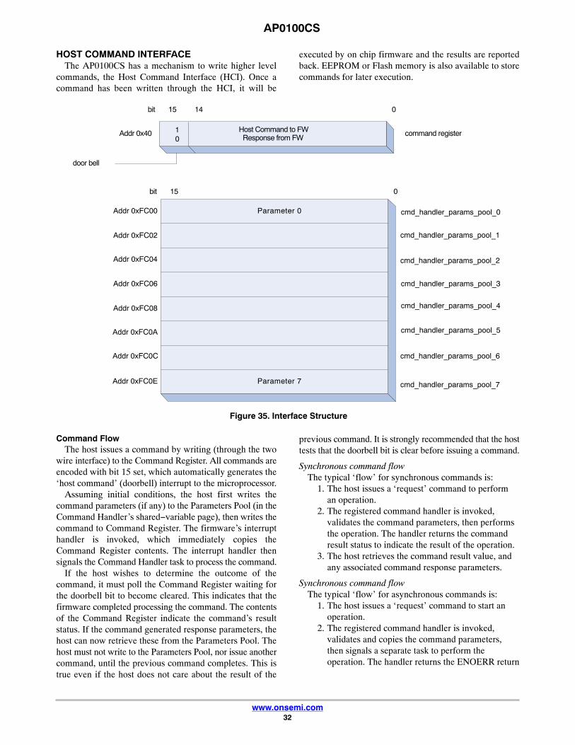
HOST COMMAND INTERFACEThe AP0100CS has a mechanism to write higher level
commands, the Host Command Interface (HCI). Once acommand has been written through the HCI, it will be
executed by on chip firmware and the results are reportedback. EEPROM or Flash memory is also available to storecommands for later execution.
Figure 35. Interface Structure
Host Command to FWResponse from FW
15 0bit
10
command registerAddr 0x40
Addr 0xFC00
Addr 0xFC0E
Addr 0xFC02
Addr 0xFC04
Addr 0xFC06
Addr 0xFC08
Addr 0xFC0A
Addr 0xFC0C
14
door bell
15 0bit
Parameter 0
Parameter 7
cmd_handler_params_pool_0
cmd_handler_params_pool_3
cmd_handler_params_pool_4
cmd_handler_params_pool_5
cmd_handler_params_pool_1
cmd_handler_params_pool_2
cmd_handler_params_pool_6
cmd_handler_params_pool_7
Command FlowThe host issues a command by writing (through the two
wire interface) to the Command Register. All commands areencoded with bit 15 set, which automatically generates the‘host command’ (doorbell) interrupt to the microprocessor.
Assuming initial conditions, the host first writes thecommand parameters (if any) to the Parameters Pool (in theCommand Handler’s shared−variable page), then writes thecommand to Command Register. The firmware’s interrupthandler is invoked, which immediately copies theCommand Register contents. The interrupt handler thensignals the Command Handler task to process the command.
If the host wishes to determine the outcome of thecommand, it must poll the Command Register waiting forthe doorbell bit to become cleared. This indicates that thefirmware completed processing the command. The contentsof the Command Register indicate the command’s resultstatus. If the command generated response parameters, thehost can now retrieve these from the Parameters Pool. Thehost must not write to the Parameters Pool, nor issue anothercommand, until the previous command completes. This istrue even if the host does not care about the result of the
previous command. It is strongly recommended that the hosttests that the doorbell bit is clear before issuing a command.
Synchronous command flowThe typical ‘flow’ for synchronous commands is:
1. The host issues a ‘request’ command to performan operation.
2. The registered command handler is invoked,validates the command parameters, then performsthe operation. The handler returns the commandresult status to indicate the result of the operation.
3. The host retrieves the command result value, andany associated command response parameters.
Synchronous command flowThe typical ‘flow’ for asynchronous commands is:
1. The host issues a ‘request’ command to start anoperation.
2. The registered command handler is invoked,validates and copies the command parameters,then signals a separate task to perform theoperation. The handler returns the ENOERR return
AP0100CS
www.onsemi.com33
value to indicate the command was acceptable andis in progress.
3. The host retrieves the command return value – if itis not ENOERR the host knows that the commandwas not accepted and is not in progress.
4. Subsequently, the host issues an appropriate ‘getstatus’ command to both poll whether thecommand has completed, and if so, retrieve anyassociated response parameters.
5. The registered command handler is invoked,determines the state of the command (via sharedvariables with the processing task), and returnseither ‘EBUSY’ to indicate the command is still inprogress, or it returns the result status of thecommand.
6. The host must re−issue the ‘get status’ commanduntil it does not receive the EBUSY response.
Asynchronous commands exist to allow the Host to issuemultiple commands to the various subsystems withouthaving to wait for each command to complete. This preventsthe host command interface from being blocked by along−running command. Therefore, each asynchronouscommand has a “Get Status” (or similar) command to allowthe Host to determine when the asynchronous commandcompletes.
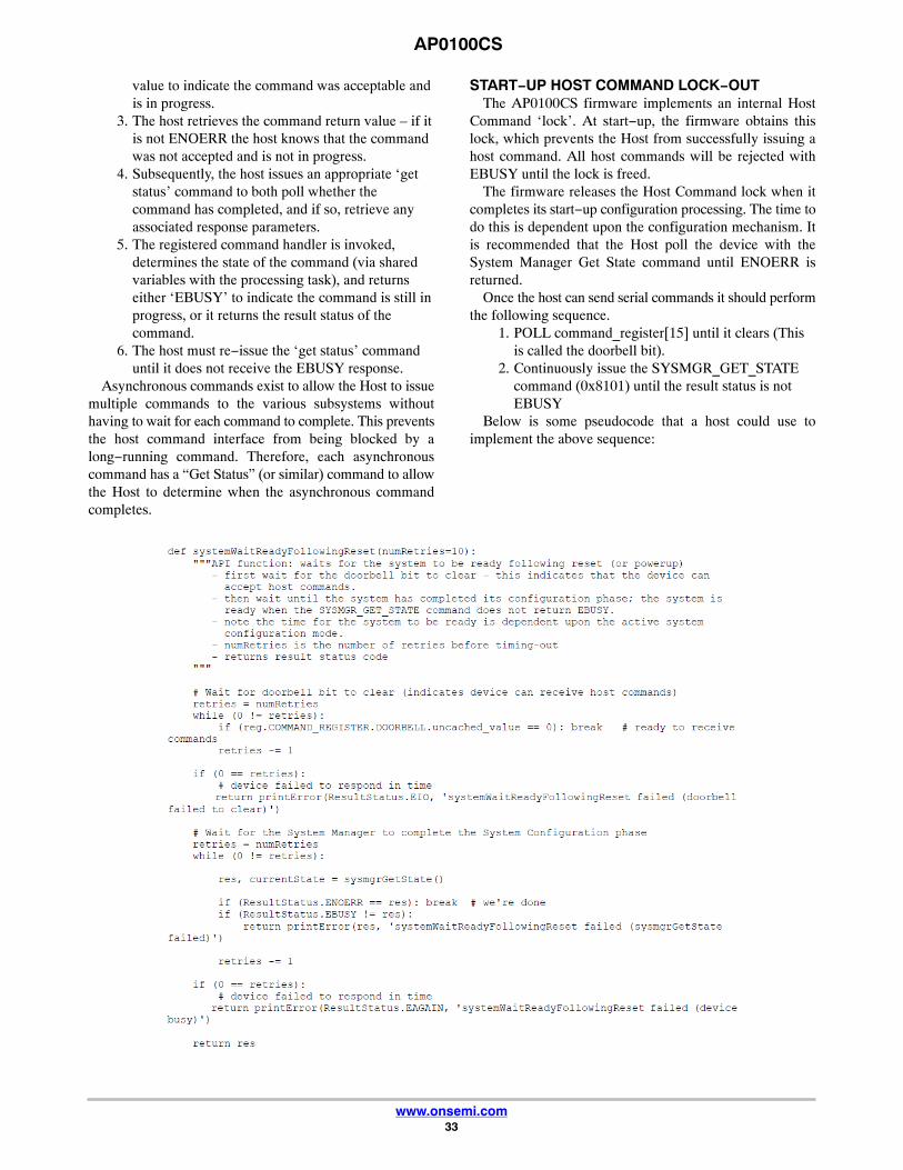
START−UP HOST COMMAND LOCK−OUTThe AP0100CS firmware implements an internal Host
Command ‘lock’. At start−up, the firmware obtains thislock, which prevents the Host from successfully issuing ahost command. All host commands will be rejected withEBUSY until the lock is freed.
The firmware releases the Host Command lock when itcompletes its start−up configuration processing. The time todo this is dependent upon the configuration mechanism. Itis recommended that the Host poll the device with theSystem Manager Get State command until ENOERR isreturned.
Once the host can send serial commands it should performthe following sequence.
1. POLL command_register[15] until it clears (Thisis called the doorbell bit).
2. Continuously issue the SYSMGR_GET_STATEcommand (0x8101) until the result status is notEBUSY
Below is some pseudocode that a host could use toimplement the above sequence:
AP0100CS
www.onsemi.com34
MULTITASKINGThe AP0100CS firmware is multitasking; therefore note
that it is possible for an internally requested command to bein−progress when the Host issues a command. In thesecircumstances, the Host command is immediately rejectedwith EBUSY. The Host should reissue the command after ashort interval.
HOST COMMANDS
OverviewThe AP0100CS supports a number of functional modules
or processing subsystems. Each module or subsystem
exposes commands to the host to control and configure itsoperation.
Command ParametersCommand parameters are written to the Parameters Pool
shared−variables by the host prior to invoking the command.Similarly, any Command Response parameters are alsowritten back to the Parameters Pool by the firmware.
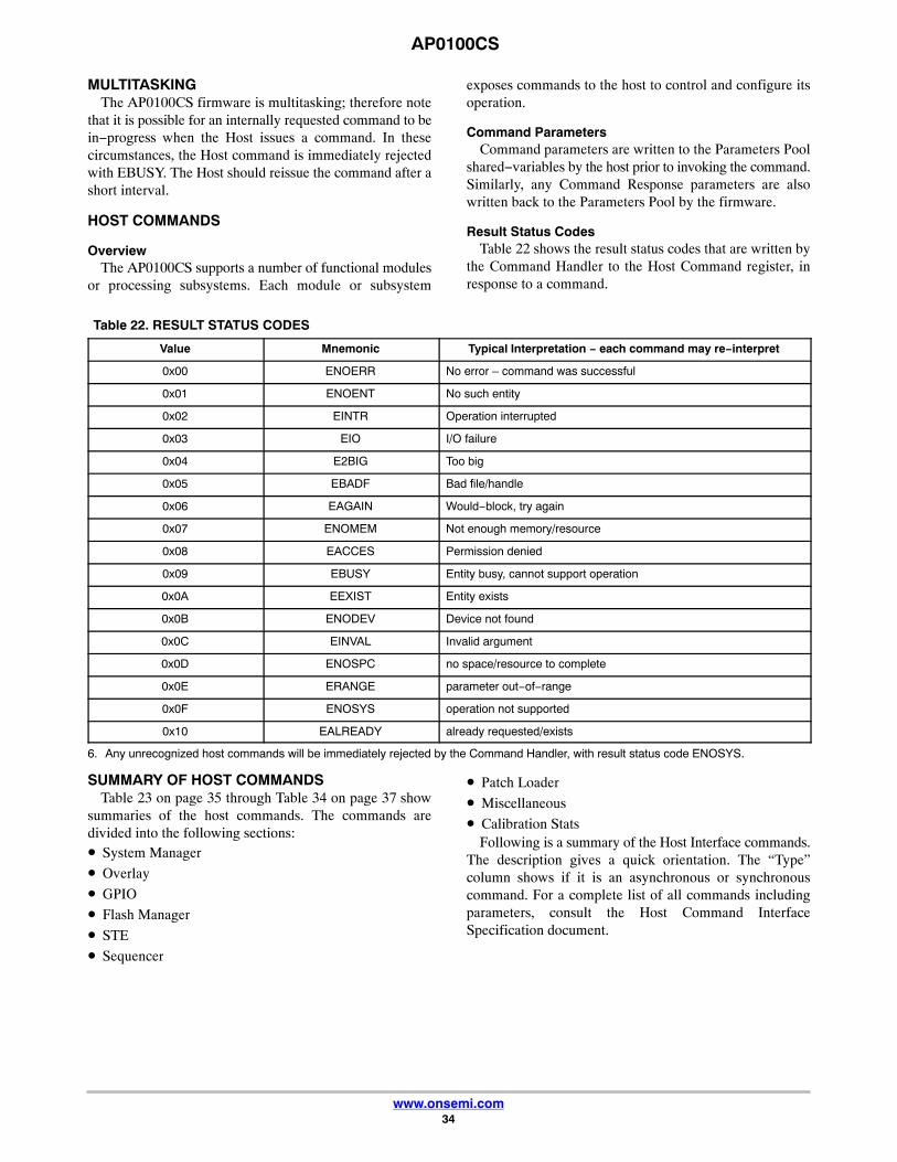
Result Status CodesTable 22 shows the result status codes that are written by
the Command Handler to the Host Command register, inresponse to a command.
Table 22. RESULT STATUS CODES
Value Mnemonic Typical Interpretation − each command may re−interpret
0x00 ENOERR No error – command was successful
0x01 ENOENT No such entity
0x02 EINTR Operation interrupted
0x03 EIO I/O failure
0x04 E2BIG Too big
0x05 EBADF Bad file/handle
0x06 EAGAIN Would−block, try again
0x07 ENOMEM Not enough memory/resource
0x08 EACCES Permission denied
0x09 EBUSY Entity busy, cannot support operation
0x0A EEXIST Entity exists
0x0B ENODEV Device not found
0x0C EINVAL Invalid argument
0x0D ENOSPC no space/resource to complete
0x0E ERANGE parameter out−of−range
0x0F ENOSYS operation not supported
0x10 EALREADY already requested/exists
6. Any unrecognized host commands will be immediately rejected by the Command Handler, with result status code ENOSYS.
SUMMARY OF HOST COMMANDSTable 23 on page 35 through Table 34 on page 37 show
summaries of the host commands. The commands aredivided into the following sections:• System Manager
• Overlay
• GPIO
• Flash Manager
• STE
• Sequencer
• Patch Loader
• Miscellaneous
• Calibration StatsFollowing is a summary of the Host Interface commands.
The description gives a quick orientation. The “Type”column shows if it is an asynchronous or synchronouscommand. For a complete list of all commands includingparameters, consult the Host Command InterfaceSpecification document.
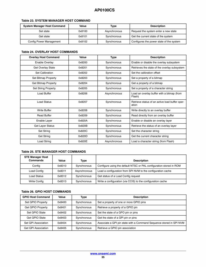
AP0100CS
www.onsemi.com35
Table 23. SYSTEM MANAGER HOST COMMAND
System Manager Host Command Value Type Description
Set state 0x8100 Asynchronous Request the system enter a new state
Get state 0x8101 Synchronous Get the current state of the system
Config Power Management 0x8102 Synchronous Configures the power state of the system
Table 24. OVERLAY HOST COMMANDS
Overlay Host Command Value Type Description
Enable Overlay 0x8200 Synchronous Enable or disable the overlay subsystem
Get Overlay State 0x8201 Synchronous Retrieves the state of the overlay subsystem
Set Calibration 0x8202 Synchronous Set the calibration offset
Set Bitmap Property 0x8203 Synchronous Set a property of a bitmap
Get Bitmap Property 0x8204 Synchronous Get a property of a bitmap
Set String Property 0x8205 Synchronous Set a property of a character string
Load Buffer 0x8206 Asynchronous Load an overlay buffer with a bitmap (fromFlash)
Load Status 0x8207 Synchronous Retrieve status of an active load buffer oper-ation
Write Buffer 0x8208 Synchronous Write directly to an overlay buffer
Read Buffer 0x8209 Synchronous Read directly from an overlay buffer
Enable Layer 0x820A Synchronous Enable or disable an overlay layer
Get Layer Status 0x820B Synchronous Retrieve the status of an overlay layer
Set String 0x820C Synchronous Set the character string
Get String 0x820D Synchronous Get the current character string
Load String 0x820E Asynchronous Load a character string (from Flash)
Table 25. STE MANAGER HOST COMMANDS
STE Manager HostCommands Value Type Description
Config 0x8310 Synchronous Configure using the default NTSC or PAL configuration stored in ROM
Load Config 0x8311 Asynchronous Load a configuration from SPI NVM to the configuration cache
Load Status 0x8312 Synchronous Get status of a Load Config request
Write Config 0x8313 Synchronous Write a configuration (via CCIS) to the configuration cache
Table 26. GPIO HOST COMMANDS
GPIO Host Command Value Type Description
Set GPIO Property 0x8400 Synchronous Set a property of one or more GPIO pins
Get GPIO Property 0x8401 Synchronous Retrieve a property of a GPIO pin
Set GPIO State 0x8402 Synchronous Set the state of a GPO pin or pins
Get GPIO State 0x8403 Synchronous Get the state of a GPI pin or pins
Set GPI Association 0x8404 Synchronous Associate a GPI pin state with a Command Sequence stored in SPI NVM
Get GPI Association 0x8405 Synchronous Retrieve a GPIO pin association

AP0100CS
www.onsemi.com36
Table 27. FLASH MANAGER HOST COMMAND
Flash Mgr Host Com-mand Value Type Description
Get Lock 0x8500 Asynchronous Request the Flash Manager access lock
Lock Status 0x8501 Synchronous Retrieve the status of the access lock request
Release Lock 0x8502 Synchronous Release the Flash Manager access lock
Config 0x8503 Synchronous Configure the Flash Manager and underlying SPI NVM subsystem
Read 0x8504 Asynchronous Read data from the SPI NVM
Write 0x8505 Asynchronous Write data to the SPI NVM
Erase Block 0x8506 Asynchronous Erase a block of data from the SPI NVM
Erase Device 0x8507 Asynchronous Erase the SPI NVM device
Query Device 0x8508 Asynchronous Query device−specific information
Status 0x8509 Synchronous Obtain status of current asynchronous operation
Config Device 0x850A Synchronous Configure the attached SPI NVM device
Table 28. SEQUENCER HOST COMMAND
Sequencer HostCommand Value Type Description
Refresh 0x8606 Asynchronous Refresh the automatic image processing algorithm configuration
Refresh Status 0x8607 Synchronous Retrieve the status of the last Refresh operation
Table 29. PATCH LOADER HOST COMMAND
Sequencer HostCommand Value Type Description
Load Patch 0x8700 Asynchronous Load a patch from SPI NVM and automatically apply
Status 0x8701 Synchronous Get status of an active Load Patch or Apply Patch request
Apply Patch 0x8702 Asynchronous Apply a patch (already located in Patch RAM)
Reserve RAM 0x8706 Synchronous Reserve RAM to contain a patch
Table 30. MISCELLANEOUS HOST COMMAND
Miscellaneous HostCommand Value Type Description
Invoke Command Seq 0x8900 Synchronous Invoke a sequence of commands stored in SPI NVM
Config Command SeqProcessor
0x8901 Synchronous Configures the Command Sequence processor
Wait for Event 0x8902 Synchronous Wait for a system event to be signalled
Table 31. CALIBRATION STATS HOST COMMANDS
Calibration StatsHost Command Value Type Description
Calib Stats Control 0x8B00 Asynchronous Start statistics gathering
Calib Stats Read 0x8B01 Synchronous Read the results back
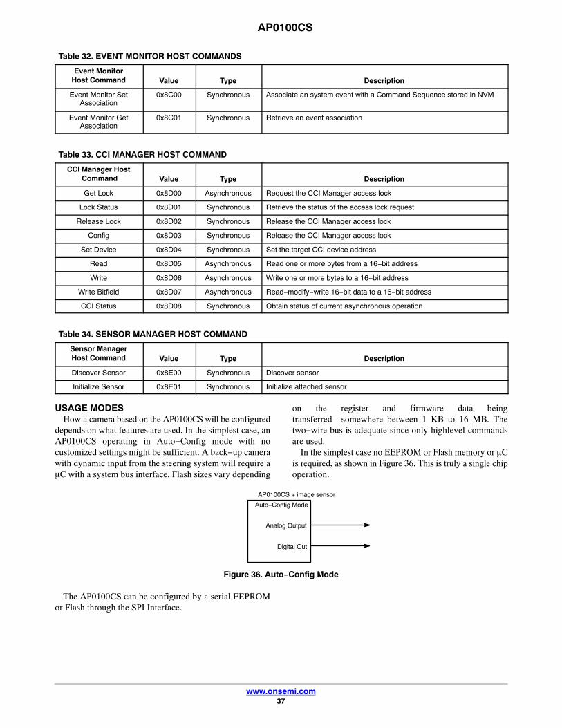
AP0100CS
www.onsemi.com37
Table 32. EVENT MONITOR HOST COMMANDS
Event MonitorHost Command Value Type Description
Event Monitor SetAssociation
0x8C00 Synchronous Associate an system event with a Command Sequence stored in NVM
Event Monitor GetAssociation
0x8C01 Synchronous Retrieve an event association
Table 33. CCI MANAGER HOST COMMAND
CCI Manager Host Command Value Type Description
Get Lock 0x8D00 Asynchronous Request the CCI Manager access lock
Lock Status 0x8D01 Synchronous Retrieve the status of the access lock request
Release Lock 0x8D02 Synchronous Release the CCI Manager access lock
Config 0x8D03 Synchronous Release the CCI Manager access lock
Set Device 0x8D04 Synchronous Set the target CCI device address
Read 0x8D05 Asynchronous Read one or more bytes from a 16−bit address
Write 0x8D06 Asynchronous Write one or more bytes to a 16−bit address
Write Bitfield 0x8D07 Asynchronous Read−modify−write 16−bit data to a 16−bit address
CCI Status 0x8D08 Synchronous Obtain status of current asynchronous operation
Table 34. SENSOR MANAGER HOST COMMAND
Sensor ManagerHost Command Value Type Description
Discover Sensor 0x8E00 Synchronous Discover sensor
Initialize Sensor 0x8E01 Synchronous Initialize attached sensor
USAGE MODESHow a camera based on the AP0100CS will be configured
depends on what features are used. In the simplest case, anAP0100CS operating in Auto−Config mode with nocustomized settings might be sufficient. A back−up camerawith dynamic input from the steering system will require a�C with a system bus interface. Flash sizes vary depending
on the register and firmware data beingtransferred—somewhere between 1 KB to 16 MB. Thetwo−wire bus is adequate since only highlevel commandsare used.
In the simplest case no EEPROM or Flash memory or �Cis required, as shown in Figure 36. This is truly a single chipoperation.
Figure 36. Auto−Config Mode
Auto−Config Mode
AP0100CS + image sensor
Digital Out
Analog Output
The AP0100CS can be configured by a serial EEPROMor Flash through the SPI Interface.
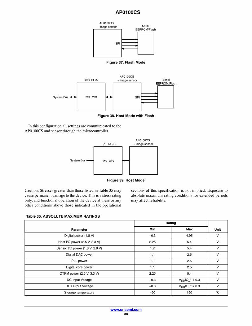
AP0100CS
www.onsemi.com38
Figure 37. Flash Mode
AP0100CS + image sensor Serial
EEPROM/Flash
SPI
System Bus two−wire
Figure 38. Host Mode with Flash
SPI
AP0100CS + image sensor Serial
EEPROM/Flash8/16 bit �C
In this configuration all settings are communicated to theAP0100CS and sensor through the microcontroller.
Figure 39. Host Mode
System Bus
AP0100CS + image sensor8/16 bit �C
two−wire
Caution: Stresses greater than those listed in Table 35 maycause permanent damage to the device. This is a stress ratingonly, and functional operation of the device at these or anyother conditions above those indicated in the operational
sections of this specification is not implied. Exposure toabsolute maximum rating conditions for extended periodsmay affect reliability.
Table 35. ABSOLUTE MAXIMUM RATINGS
Parameter
Rating
UnitMin Max
Digital power (1.8 V) −0.3 4.95 V
Host I/O power (2.5 V, 3.3 V) 2.25 5.4 V
Sensor I/O power (1.8 V, 2.8 V) 1.7 5.4 V
Digital DAC power 1.1 2.5 V
PLL power 1.1 2.5 V
Digital core power 1.1 2.5 V
OTPM power (2.5 V, 3.3 V) 2.25 5.4 V
DC Input Voltage −0.3 VDDIO_* + 0.3 V
DC Output Voltage −0.3 VDDIO_* + 0.3 V
Storage temperature −50 150 °C
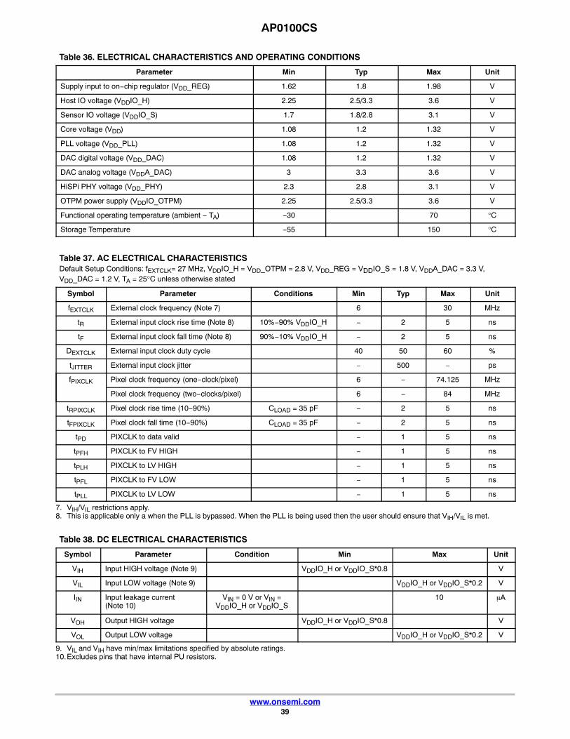
AP0100CS
www.onsemi.com39
Table 36. ELECTRICAL CHARACTERISTICS AND OPERATING CONDITIONS
Parameter Min Typ Max Unit
Supply input to on−chip regulator (VDD_REG) 1.62 1.8 1.98 V
Host IO voltage (VDDIO_H) 2.25 2.5/3.3 3.6 V
Sensor IO voltage (VDDIO_S) 1.7 1.8/2.8 3.1 V
Core voltage (VDD) 1.08 1.2 1.32 V
PLL voltage (VDD_PLL) 1.08 1.2 1.32 V
DAC digital voltage (VDD_DAC) 1.08 1.2 1.32 V
DAC analog voltage (VDDA_DAC) 3 3.3 3.6 V
HiSPi PHY voltage (VDD_PHY) 2.3 2.8 3.1 V
OTPM power supply (VDDIO_OTPM) 2.25 2.5/3.3 3.6 V
Functional operating temperature (ambient − TA) −30 70 °C
Storage Temperature −55 150 °C
Table 37. AC ELECTRICAL CHARACTERISTICSDefault Setup Conditions: fEXTCLK= 27 MHz, VDDIO_H = VDD_OTPM = 2.8 V, VDD_REG = VDDIO_S = 1.8 V, VDDA_DAC = 3.3 V,VDD_DAC = 1.2 V, TA = 25°C unless otherwise stated
Symbol Parameter Conditions Min Typ Max Unit
fEXTCLK External clock frequency (Note 7) 6 30 MHz
tR External input clock rise time (Note 8) 10%−90% VDDIO_H − 2 5 ns
tF External input clock fall time (Note 8) 90%−10% VDDIO_H − 2 5 ns
DEXTCLK External input clock duty cycle 40 50 60 %
tJITTER External input clock jitter − 500 − ps
fPIXCLK Pixel clock frequency (one−clock/pixel) 6 − 74.125 MHz
Pixel clock frequency (two−clocks/pixel) 6 − 84 MHz
tRPIXCLK Pixel clock rise time (10−90%) CLOAD = 35 pF − 2 5 ns
tFPIXCLK Pixel clock fall time (10−90%) CLOAD = 35 pF − 2 5 ns
tPD PIXCLK to data valid − 1 5 ns
tPFH PIXCLK to FV HIGH − 1 5 ns
tPLH PIXCLK to LV HIGH − 1 5 ns
tPFL PIXCLK to FV LOW − 1 5 ns
tPLL PIXCLK to LV LOW − 1 5 ns
7. VIH/VIL restrictions apply.8. This is applicable only a when the PLL is bypassed. When the PLL is being used then the user should ensure that VIH/VIL is met.
Table 38. DC ELECTRICAL CHARACTERISTICS
Symbol Parameter Condition Min Max Unit
VIH Input HIGH voltage (Note 9) VDDIO_H or VDDIO_S*0.8 V
VIL Input LOW voltage (Note 9) VDDIO_H or VDDIO_S*0.2 V
IIN Input leakage current(Note 10)
VIN = 0 V or VIN =VDDIO_H or VDDIO_S
10 �A
VOH Output HIGH voltage VDDIO_H or VDDIO_S*0.8 V
VOL Output LOW voltage VDDIO_H or VDDIO_S*0.2 V
9. VIL and VIH have min/max limitations specified by absolute ratings.10.Excludes pins that have internal PU resistors.
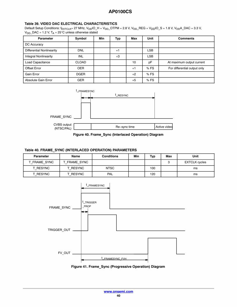
AP0100CS
www.onsemi.com40
Table 39. VIDEO DAC ELECTRICAL CHARACTERISTICSDefault Setup Conditions: fEXTCLK= 27 MHz, VDDIO_H = VDD_OTPM = 2.8 V, VDD_REG = VDDIO_S = 1.8 V, VDDA_DAC = 3.3 V,VDD_DAC = 1.2 V, TA = 25°C unless otherwise stated
Parameter Symbol Min Typ Max Unit Comments
DC Accuracy
Differential Nonlinearity DNL +1 LSB
Integral Nonlinearity INL +3 LSB
Load Capacitance CLOAD 10 pF At maximum output current
Offset Error OER +1 % FS For differential output only
Gain Error DGER +2 % FS
Absolute Gain Error GER +5 % FS
FRAME_SYNC
Figure 40. Frame_Sync (Interlaced Operation) Diagram
CVBS output(NTSC/PAL) Re−sync time Active video
t_FRAMESYNCt_RESYNC
Table 40. FRAME_SYNC (INTERLACED OPERATION) PARAMETERS
Parameter Name Conditions Min Typ Max Unit
T_FRAME_SYNC T_FRAME_SYNC 3 EXTCLK cycles
T_RESYNC T_RESYNC NTSC 100 ms
T_RESYNC T_RESYNC PAL 120 ms
FRAME_SYNC
Figure 41. Frame_Sync (Progressive Operation) Diagram
t_FRAMESYNC
t_TRIGGER
_PROP
t_FRAMESYNC_FVH
TRIGGER_OUT
FV_OUT
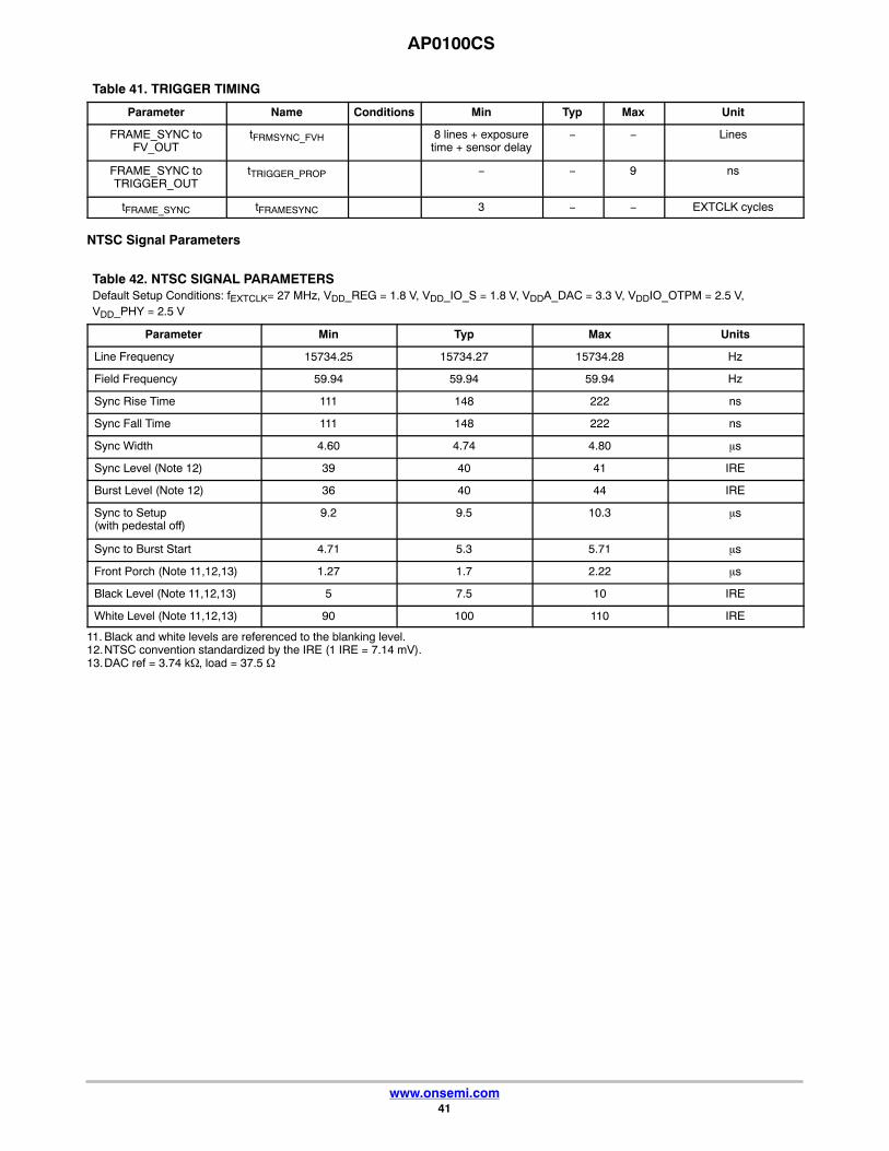
AP0100CS
www.onsemi.com41
Table 41. TRIGGER TIMING
Parameter Name Conditions Min Typ Max Unit
FRAME_SYNC toFV_OUT
tFRMSYNC_FVH 8 lines + exposuretime + sensor delay
− − Lines
FRAME_SYNC toTRIGGER_OUT
tTRIGGER_PROP − − 9 ns
tFRAME_SYNC tFRAMESYNC 3 − − EXTCLK cycles
NTSC Signal Parameters
Table 42. NTSC SIGNAL PARAMETERSDefault Setup Conditions: fEXTCLK= 27 MHz, VDD_REG = 1.8 V, VDD_IO_S = 1.8 V, VDDA_DAC = 3.3 V, VDDIO_OTPM = 2.5 V,VDD_PHY = 2.5 V
Parameter Min Typ Max Units
Line Frequency 15734.25 15734.27 15734.28 Hz
Field Frequency 59.94 59.94 59.94 Hz
Sync Rise Time 111 148 222 ns
Sync Fall Time 111 148 222 ns
Sync Width 4.60 4.74 4.80 �s
Sync Level (Note 12) 39 40 41 IRE
Burst Level (Note 12) 36 40 44 IRE
Sync to Setup(with pedestal off)
9.2 9.5 10.3 �s
Sync to Burst Start 4.71 5.3 5.71 �s
Front Porch (Note 11,12,13) 1.27 1.7 2.22 �s
Black Level (Note 11,12,13) 5 7.5 10 IRE
White Level (Note 11,12,13) 90 100 110 IRE
11. Black and white levels are referenced to the blanking level.12.NTSC convention standardized by the IRE (1 IRE = 7.14 mV).13.DAC ref = 3.74 k�, load = 37.5 �
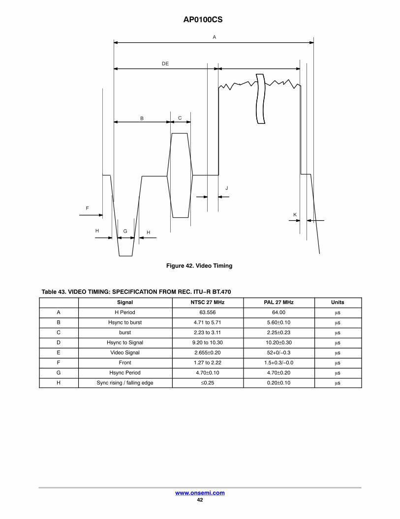
AP0100CS
www.onsemi.com42
Figure 42. Video Timing
H
F
A
H
DE
B C
G
J
K
Table 43. VIDEO TIMING: SPECIFICATION FROM REC. ITU−R BT.470
Signal NTSC 27 MHz PAL 27 MHz Units
A H Period 63.556 64.00 �s
B Hsync to burst 4.71 to 5.71 5.60±0.10 �s
C burst 2.23 to 3.11 2.25±0.23 �s
D Hsync to Signal 9.20 to 10.30 10.20±0.30 �s
E Video Signal 2.655±0.20 52+0/−0.3 �s
F Front 1.27 to 2.22 1.5+0.3/−0.0 �s
G Hsync Period 4.70±0.10 4.70±0.20 �s
H Sync rising / falling edge ≤0.25 0.20±0.10 �s
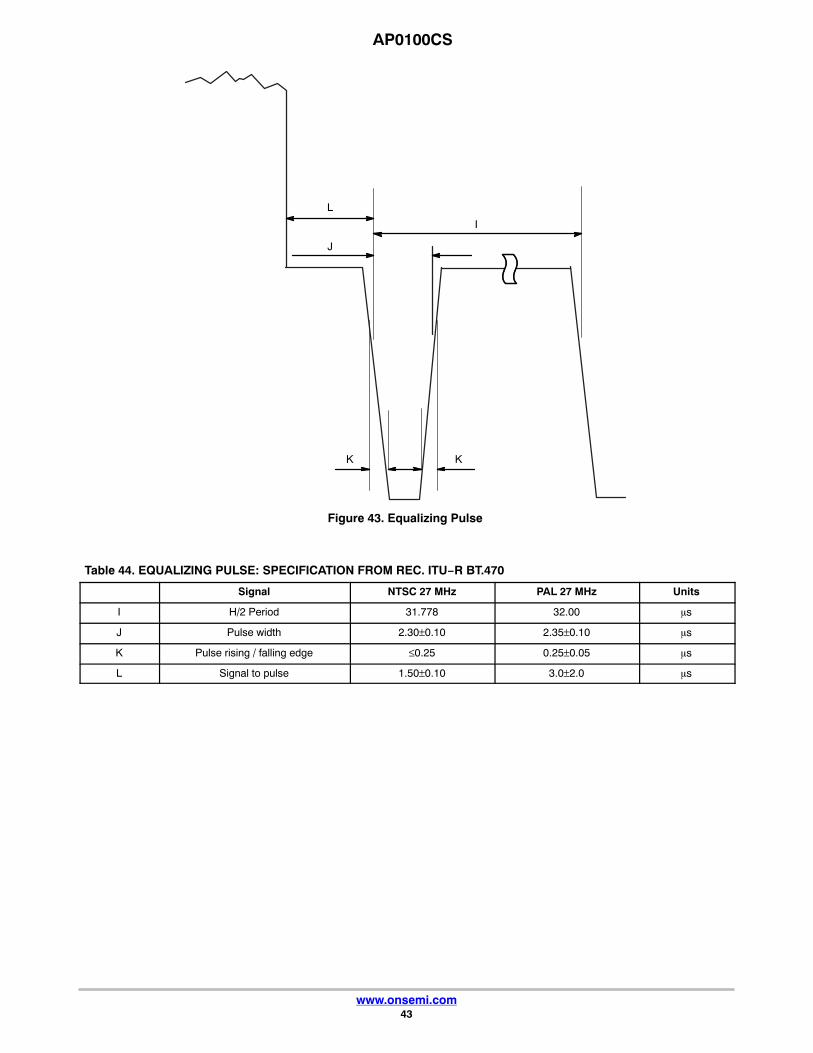
AP0100CS
www.onsemi.com43
Figure 43. Equalizing Pulse
L
I
J
K K
Table 44. EQUALIZING PULSE: SPECIFICATION FROM REC. ITU−R BT.470
Signal NTSC 27 MHz PAL 27 MHz Units
I H/2 Period 31.778 32.00 �s
J Pulse width 2.30±0.10 2.35±0.10 �s
K Pulse rising / falling edge ≤0.25 0.25±0.05 �s
L Signal to pulse 1.50±0.10 3.0±2.0 �s
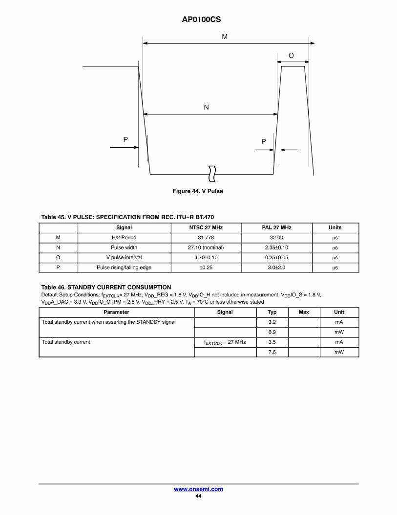
AP0100CS
www.onsemi.com44
Figure 44. V Pulse
N
M
O
P P
Table 45. V PULSE: SPECIFICATION FROM REC. ITU−R BT.470
Signal NTSC 27 MHz PAL 27 MHz Units
M H/2 Period 31.778 32.00 �s
N Pulse width 27.10 (nominal) 2.35±0.10 �s
O V pulse interval 4.70±0.10 0.25±0.05 �s
P Pulse rising/falling edge ≤0.25 3.0±2.0 �s
Table 46. STANDBY CURRENT CONSUMPTIONDefault Setup Conditions: fEXTCLK= 27 MHz, VDD_REG = 1.8 V, VDDIO_H not included in measurement, VDDIO_S = 1.8 V, VDDA_DAC = 3.3 V, VDDIO_OTPM = 2.5 V, VDD_PHY = 2.5 V, TA = 70°C unless otherwise stated
Parameter Signal Typ Max Unit
Total standby current when asserting the STANDBY signal 3.2 mA
6.9 mW
Total standby current fEXTCLK = 27 MHz 3.5 mA
7.6 mW

AP0100CS
www.onsemi.com45
Table 47. OPERATING CURRENT CONSUMPTIONDefault Setup Conditions: fEXTCLK= 27 MHz, VDD_REG = 1.8 V; VDDIO_H not included in measurementVDDIO_S = 1.8 V, VDDA_DAC = 3.3 V, VDDIO_OTPM = 2.5 V, VDD_PHY = 2.5 V, TA = 70°C unless otherwise stated
Symbol Conditions Min Typ Max Unit
VDD_REG 1.62 1.8 1.98 V
VDDIO_H = 2.5 V 2.25 2.5 2.75 V
VDDIO_H = 3.3 V 3 3.3 3.6 V
VDDIO_S = 1.8 V 1.7 1.8 1.9 V
VDDIO_S = 2.8 V 2.5 2.8 3.1 V
VDDIO_OTPM = 2.5 V 2.25 2.5 2.75 V
VDDIO_OTPM = 3.3 V 3 3.3 3.6 V
VDDA_DAC 3 3.3 3.6 V
VDD_PHY 2.3 2.8 3.1 V
IDD_REG NTSC HiSPi 12−bit 63.7 mA
NTSC HiSPi 14−bit 63.6 mA
NTSC 64.1 mA
PAL 59.5 mA
IDDIO_S NTSC HiSPi 12−bit 3.2 mA
NTSC HiSPi 14−bit 3.2 mA
NTSC 3.3 mA
PAL 3.3 mA
IDDIO_OTPM NTSC HiSPi 12−bit 0.1 mA
NTSC HiSPi 14−bit 0.1 mA
NTSC 0.1 mA
PAL 0.1 mA
IDDA_DAC NTSC HiSPi 12−bit 1.2 19.54 mA
NTSC HiSPi 14−bit 1.2 19.54 mA
NTSC 1.2 19.54 mA
PAL 1.2 19.54 mA
IDD_PHY NTSC HiSPi 12−bit 0.3 mA
NTSC HiSPi 14−bit 0.3 mA
NTSC 0.0 mA
PAL 0.0 mA
Total powerconsumption
NTSC HiSPi 12−bit 185.66 mW
NTSC HiSPi 14−bit 185.56 mW
NTSC 185.56 mW
PAL 177.46 mW
14.R_DAC_POS = 75 �, R_DAC_NEG = 37.5 �, R_DAC_REF= 3.74 k�15.Current in single ended mode. When in differential mode the current will be 37.9 mA
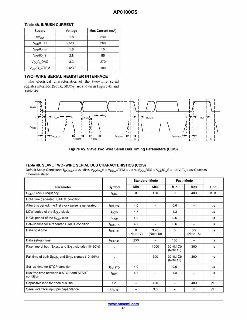
AP0100CS
www.onsemi.com46
Table 48. INRUSH CURRENT
Supply Voltage Max Current (mA)
AVDD 1.8 240
VDDIO_H 2.5/3.3 260
VDDIO_S 1.8 15
VDDIO_S 2.8 55
VDDA_DAC 3.3 270
VDDIO_OTPM 2.5/3.3 180
TWO−WIRE SERIAL REGISTER INTERFACEThe electrical characteristics of the two−wire serial
register interface (SCLK, SDATA) are shown in Figure 45 andTable 49.
Figure 45. Slave Two Wire Serial Bus Timing Parameters (CCIS)
SDATA
SCLK
tf tLOW tr tSU;DATtf tHD;STA tr tBUF
StHD;STA
tHD;DAT tHIGHtSU;STA
SrtSU;STO
P S
Table 49. SLAVE TWO−WIRE SERIAL BUS CHARACTERISTICS (CCIS) Default Setup Conditions: fEXTCLK = 27 MHz, VDDIO_H = VDD_OTPM = 2.8 V, VDD_REG = VDDIO_S = 1.8 V, TA = 25°C unlessotherwise stated
Parameter Symbol
Standard−Mode Fast−Mode
UnitMin Max Min Max
SCLK Clock Frequency fSCL 0 100 0 400 KHz
Hold time (repeated) START condition
After this period, the first clock pulse is generated tHD;STA 4.0 − 0.6 − �s
LOW period of the SCLK clock tLOW 4.7 − 1.3 − �s
HIGH period of the SCLK clock tHIGH 4.0 − 0.6 − �s
Set−up time for a repeated START condition tSU;STA 4.7 − 0.6 − �s
Data hold time tHD;DAT 0(Note 17)
3.45(Note 18)
0 0.9(Note 18)
�s
Data set−up time tSU;DAT 250 − 100 − ns
Rise time of both SDATA and SCLK signals (10−90%) tr − 1000 20+0.1Cb(Note 19)
300 ns
Fall time of both SDATA and SCLK signals (10−90%) tf − 300 20+0.1Cb(Note 19)
300 ns
Set−up time for STOP condition tSU;STO 4.0 − 0.6 − �s
Bus free time between a STOP and STARTcondition
tBUF 4.7 − 1.3 − �s
Capacitive load for each bus line Cb − 400 − 400 pF
Serial interface input pin capacitance CIN SI − 3.3 − 3.3 pF
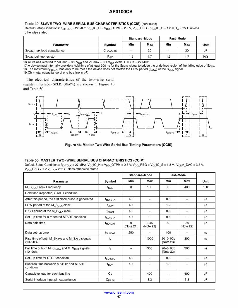
AP0100CS
www.onsemi.com47
Table 49. SLAVE TWO−WIRE SERIAL BUS CHARACTERISTICS (CCIS) (continued)Default Setup Conditions: fEXTCLK = 27 MHz, VDDIO_H = VDD_OTPM = 2.8 V, VDD_REG = VDDIO_S = 1.8 V, TA = 25°C unlessotherwise stated
Parameter Unit
Fast−ModeStandard−Mode
SymbolParameter UnitMaxMinMaxMinSymbol
SDATA max load capacitance CLOAD SD − 30 − 30 pF
SDATA pull−up resistor RSD 1.5 4.7 1.5 4.7 K�
16.All values referred to VIHmin = 0.9 VDD and VILmax = 0.1 VDD levels. EXCLK = 27 MHz.17.A device must internally provide a hold time of at least 300 ns for the SDATA signal to bridge the undefined region of the falling edge of SCLK.18.The maximum tHD;DAT has only to be met if the device does not stretch the LOW period (tLOW) of the SCLK signal.19.Cb = total capacitance of one bus line in pF.
The electrical characteristics of the two−wire serialregister interface (SCLK, SDATA) are shown in Figure 46and Table 50.
Figure 46. Master Two Wire Serial Bus Timing Parameters (CCIS)
SDATA
SCLK
tf tLOW tr tSU;DATtf tHD;STA tr tBUF
StHD;STA
tHD;DAT tHIGHtSU;STA
SrtSU;STO
P S
Table 50. MASTER TWO−WIRE SERIAL BUS CHARACTERISTICS (CCIM) Default Setup Conditions: fEXTCLK = 27 MHz, VDDIO_H = VDD_OTPM = 2.8 V, VDD_REG = VDDIO_S = 1.8 V, VDDA_DAC = 3.3 V,VDD_DAC = 1.2 V, TA = 25°C unless otherwise stated
Parameter Symbol
Standard−Mode Fast−Mode
UnitMin Max Min Max
M_SCLK Clock Frequency fSCL 0 100 0 400 KHz
Hold time (repeated) START condition
After this period, the first clock pulse is generated tHD;STA 4.0 − 0.6 − �s
LOW period of the M_SCLK clock tLOW 4.7 − 1.2 − �s
HIGH period of the M_SCLK clock tHIGH 4.0 − 0.6 − �s
Set−up time for a repeated START condition tSU;STA 4.7 − 0.6 − �s
Data hold time tHD;DAT 0(Note 21)
3.45(Note 22)
0 0.9(Note 22)
�s
Data set−up time tSU;DAT 250 − 100 − ns
Rise time of both M_SDATA and M_SCLK signals(10−90%)
tr − 1000 20+0.1Cb(Note 23)
300 ns
Fall time of both M_SDATA and M_SCLK signals(10−90%)
tf − 300 20+0.1Cb(Note 23)
300 ns
Set−up time for STOP condition tSU;STO 4.0 − 0.6 − �s
Bus free time between a STOP and STARTcondition
tBUF 4.7 − 1.3 − �s
Capacitive load for each bus line Cb − 400 − 400 pF
Serial interface input pin capacitance CIN_SI − 3.3 − 3.3 pF
AP0100CS
www.onsemi.com48
Table 50. MASTER TWO−WIRE SERIAL BUS CHARACTERISTICS (CCIM) (continued)Default Setup Conditions: fEXTCLK = 27 MHz, VDDIO_H = VDD_OTPM = 2.8 V, VDD_REG = VDDIO_S = 1.8 V, VDDA_DAC = 3.3 V,VDD_DAC = 1.2 V, TA = 25°C unless otherwise stated
Parameter Unit
Fast−ModeStandard−Mode
SymbolParameter UnitMaxMinMaxMinSymbol
M_SDATA max load capacitance CLOAD_SD − 30 − 30 pF
M_SDATA pull−up resistor RSD 1.5 4.7 1.5 4.7 K�
20.All values referred to VIHmin = 0.9 VDD and VILmax = 0.1 VDD levels. EXCLK = 27 MHz.21.A device must internally provide a hold time of at least 300 ns for the M_SDATA signal to bridge the undefined region of the falling edge of
M_SCLK.22.The maximum tHD;DAT has only to be met if the device does not stretch the LOW period (tLOW) of the M_SCLK signal.23.Cb = total capacitance of one bus line in pF.
VFBGA100 7x7CASE 138AH
ISSUE ODATE 30 DEC 2014
MECHANICAL CASE OUTLINE
PACKAGE DIMENSIONS
ON Semiconductor and are trademarks of Semiconductor Components Industries, LLC dba ON Semiconductor or its subsidiaries in the United States and/or other countries.ON Semiconductor reserves the right to make changes without further notice to any products herein. ON Semiconductor makes no warranty, representation or guarantee regardingthe suitability of its products for any particular purpose, nor does ON Semiconductor assume any liability arising out of the application or use of any product or circuit, and specificallydisclaims any and all liability, including without limitation special, consequential or incidental damages. ON Semiconductor does not convey any license under its patent rights nor therights of others.
98AON93700FDOCUMENT NUMBER:
DESCRIPTION:
Electronic versions are uncontrolled except when accessed directly from the Document Repository.Printed versions are uncontrolled except when stamped “CONTROLLED COPY” in red.
PAGE 1 OF 1VFBGA100 7X7
© Semiconductor Components Industries, LLC, 2019 www.onsemi.com

onsemi, , and other names, marks, and brands are registered and/or common law trademarks of Semiconductor Components Industries, LLC dba “onsemi” or its affiliatesand/or subsidiaries in the United States and/or other countries. onsemi owns the rights to a number of patents, trademarks, copyrights, trade secrets, and other intellectual property.A listing of onsemi’s product/patent coverage may be accessed at www.onsemi.com/site/pdf/Patent−Marking.pdf. onsemi reserves the right to make changes at any time to anyproducts or information herein, without notice. The information herein is provided “as−is” and onsemi makes no warranty, representation or guarantee regarding the accuracy of theinformation, product features, availability, functionality, or suitability of its products for any particular purpose, nor does onsemi assume any liability arising out of the application or useof any product or circuit, and specifically disclaims any and all liability, including without limitation special, consequential or incidental damages. Buyer is responsible for its productsand applications using onsemi products, including compliance with all laws, regulations and safety requirements or standards, regardless of any support or applications informationprovided by onsemi. “Typical” parameters which may be provided in onsemi data sheets and/or specifications can and do vary in different applications and actual performance mayvary over time. All operating parameters, including “Typicals” must be validated for each customer application by customer’s technical experts. onsemi does not convey any licenseunder any of its intellectual property rights nor the rights of others. onsemi products are not designed, intended, or authorized for use as a critical component in life support systemsor any FDA Class 3 medical devices or medical devices with a same or similar classification in a foreign jurisdiction or any devices intended for implantation in the human body. ShouldBuyer purchase or use onsemi products for any such unintended or unauthorized application, Buyer shall indemnify and hold onsemi and its officers, employees, subsidiaries, affiliates,and distributors harmless against all claims, costs, damages, and expenses, and reasonable attorney fees arising out of, directly or indirectly, any claim of personal injury or deathassociated with such unintended or unauthorized use, even if such claim alleges that onsemi was negligent regarding the design or manufacture of the part. onsemi is an EqualOpportunity/Affirmative Action Employer. This literature is subject to all applicable copyright laws and is not for resale in any manner.
PUBLICATION ORDERING INFORMATIONTECHNICAL SUPPORTNorth American Technical Support:Voice Mail: 1 800−282−9855 Toll Free USA/CanadaPhone: 011 421 33 790 2910
LITERATURE FULFILLMENT:Email Requests to: [email protected]
onsemi Website: www.onsemi.com
Europe, Middle East and Africa Technical Support:Phone: 00421 33 790 2910For additional information, please contact your local Sales Representative
◊